Embed Size (px)
Citation preview
Chapter 8
Probe-based measurement systems
8.1 An overview of probe-based measurement systems A critical component of the near-field scanning microwave microscope (NSMM) is the broadband probe. Thus, a fundamental understanding of the probe’s near-field interaction with investigated materials and devices is necessary for interpretation of NSMM measurements. In this chapter, we will discuss the fundamental concepts and modeling of probe-based measurement systems. We will place particular emphasis on near-field probes that are similar to atomic force microscope cantilevers, including models for local effects around the tip-apex, as well as the parasitic effects of the cantilever’s body. This introduction should serve as a foundation for understanding the application of these measurement systems to semi-quantitative and quantitative characterization of both devices and materials. In addition, we shall introduce techniques for calibration of broadband scanning probe systems that enable quantitative characterization of device and material properties. In recent years a number of variants of NSMMs have been reported. They can be distinguished based on the principles of their design. The designs include instruments based on transmission lines, [1]-[4], waveguides [5],[6], resonant cavities [4],[7] and other scanning probe microscope architectures [8]-[10]. A more complete summary of these techniques can be found in review articles [11],[12] and in the preceding chapter. In general, microwave microscopes utilize either resonant or non-resonant probes. In the case of resonant probes, changes in resonant frequency and quality factor are measured either as a sample is brought towards the probe tip or as an inhomogeneous sample is scanned laterally beneath the tip. The changes in resonant frequency and quality factor are related to the local electromagnetic properties of the sample by use of models and calibration techniques. In the case of non-resonant probes, the probe consists either of an electrically small aperture or a protruding, electrically small antenna integrated into a one- or two-port microwave network. The probe-sample coupling is characterized through position-dependent measurements of the complex reflection coefficient or complex transmission coefficient. For both resonant and non-resonant probes, in order to extract material properties of the sample, it is necessary to calculate the detailed field configuration in the probe-sample region as a function of the probe geometry, probe-to-sample distance and properties of the probed specimen. Below, we address the existing state-of-the-art models of the tip-sample interaction. This interaction has direct consequences for application and calibration of probe-based systems. We take an experimental approach based on measurement of calibration artifacts combined, where possible, with vector network analyzer (VNA) calibration procedures. In order to extract characteristic parameters from such measurements, the tip-sample interaction must be modeled and a corresponding inverse problem must be solved. As no unifying theoretical approach exists at present, we will review several different methods. Due to the near-field nature of this interaction, several different modeling approaches may be used, independently or in combination: lumped element circuits, transmission line circuits, or finite element modeling. To date, such approaches have been successful when applied to microscopes operating in reflection mode. The situation is more complicated and much less understood for transmission mode operation, lacking established procedures for calibration and device parameter extraction.

We will start with a description of the simplest models. We begin with tip-sample capacitance models, including the coupling capacitance between the tip and the sample in cases where there is a gap between the tip and the sample surface. We discuss models of the most common tip shapes and their influence on the interpretation of measurements. In the next step, we approach the microwave probing problem from the electromagnetics point of view, implementing solutions based on Maxwell’s equations. From there, we describe of existing calibration procedures for NSMMs that are being adopted for quantitative characterization of devices. In Chapter 9, we will expand on this discussion to describe particular applications to electromagnetic characterization of materials. 8.2. Simple tip-sample models. 8.2.1. General considerations Tip-sample models are indispensable for quantitative characterization of material properties. As with the modeling of microwave devices, these models can come in many forms, including analytical models, circuit models, and finite-element-based calculations. These techniques are powerful, but can’t be generalized. Therefore, one has to treat each measurement individually. Models of tip-sample interactions may be developed by use of the same commercial software programs that are used for modeling of microwave devices, albeit with many of the same restrictions and complications that were described in discussion of broadband modeling of nanoelectronic devices. In the case of near-field microscopy, the situation is slightly simplified. Due to the near-field nature of the interaction, modeling can be done without invoking full microwave solvers. Rather, the modeling can be done at a single frequency with electro- and magneto-static packages. Even in this simplified case, each particular measurement has to be considered individually with little possibility of generalization. Therefore, we will focus on simpler lumped element models and quasi-analytical approaches that have proven to be useful for the development of calibration approaches and, in turn, quantitative (or semi-quantitative) characterization. In order to get quantitative information about the device properties and introduce reasonable calibration procedures, it is necessary to capture all of the important contributions that influence the measurement in the tip-sample model. Thus, in NSMM experiments, the tip-sample interaction model embodies critical aspects of the experimental configuration. For near-field probes that are similar to atomic force microscope cantilevers, the underlying electromagnetic interaction with the sample is more or less the same for all NSMM experimental configurations, independent of whether the modeling of these interactions is based on a resonant cavity, a transmission line, or other implementation. However, the nature of probe-sample coupling and parasitic coupling within the system may vary strongly from implementation to implementation. For example, if the probe tip is not in mechanical contact with the sample (e.g. if the tip is a height h above the sample), then the electrostatic interaction of the tip with the sample, which we will refer to as the “coupling capacitance” or “coupling impedance,” must be included in addition to the sample impedance that arises from interactions within the material. In a lumped element picture, this likely will take the form of one or more capacitors. These capacitances contribute to the measured response and incorporate the influence of probe and sample geometry, as discussed further below. In addition, there are configuration-dependent, parasitic interactions of the tip with the sample that must be included in the model. To summarize, there are three major elements in a tip-sample model of a (non-contact) NSMM: the parasitic impedance, the coupling capacitance, and the impedance characterizing the sample itself. We will address all these impedances as we proceed through this chapter. We start with the coupling capacitance. The coupling capacitance is critical to calibration of NSMMs, but the coupling capacitance is

only one part of the interaction. Full calibration requires taking into account all the components of the measurement path, including those components outside of the tip-sample model such as any resonator structure. Finally, because the parasitic capacitance is common to all of the models, we will discuss it separately when addressing specific calibration techniques. 8.2.2. Coupling capacitance: parallel-plate model The natural first approximation is to model the coupling capacitance as a parallel plate capacitor with the two electrodes formed by the tip and the sample surface, respectively [13]. This approach, although somewhat crude, has been used extensively with surprisingly good results. This applies especially for cases where the objective is understanding the basic physics of a system, obtaining preliminary approximations of material parameters, or semi-quantitative estimates of relative contrast within an image. More precise models are needed to obtain the absolute values of the measured parameters. The coupling capacitance between the tip apex and sample, approximating the system as a parallel plate capacitor is
𝐶𝑎𝑝𝑒𝑥−𝑝𝑝 =𝜋𝜀0𝑅
2
ℎ , (8.1)
where R is the effective tip radius and h is the tip-sample surface distance. This approach can be improved by including a correction for the fringing capacitance. If the tip apex can be considered to be a disc-shaped terminus of a cylinder, the fringing stray capacitance of the disc can be expressed as [14]
𝐶𝑎𝑝𝑒𝑥−𝑠𝑡𝑟𝑑𝑠𝑐 = 2𝜋𝜀𝑅 ∙ 𝑙𝑛 (2𝜋𝑒𝑅
ℎ) . (8.2)
The authors of Reference [14] found empirically that the correction term
𝐶𝑎𝑝𝑒𝑥−𝑠𝑡𝑟𝑑𝑠𝑐 = 2𝜀𝑅 ∙ 𝑙𝑛 (8𝜋𝑅
𝑒ℎ) +
𝜀𝑑
𝜋∙ (ln(
ℎ
8𝜋𝑅))
2
(8.3)
provides accuracy within about 2% when R/h is on the order of unity with increased accuracy at larger R/h ratios. The resulting capacitance is the sum
𝐶𝑎𝑝𝑒𝑥 = 𝐶𝑎𝑝𝑒𝑥−𝑝𝑝 + 𝐶𝑎𝑝𝑒𝑥−𝑠𝑡𝑟𝑑𝑠𝑐 . (8.4)
Clearly, the parallel-plate approach can work well only for conducting samples. Its application for dielectric materials is limited and can be used only as a first approximation. 8.2.3. Coupling capacitance: spherical and conical tip shapes The comparison of NSMM models with experimental results clearly shows that better agreement between model and experiment can be obtained by approximating the tip apex as a sphere. In this case, one can use the method of images to model the tip-surface interaction and the corresponding coupling capacitance. The method of images is well known from electrostatics and it can be applied to broad range of materials [15]. In References [10], [16]-[18] the method of images was used to derive the apex coupling capacitance for isotropic materials and in Reference [19] the method was extended to anisotropic

dielectrics. Indeed, for many applications it is possible to get good agreement between experiments and simple analytical expressions derived by use of the method of images. For example, in the cases of a tip over a metallic or dielectric surface, the apex coupling capacitance can be expressed as
𝐶𝑎𝑝𝑒𝑥−𝑚/𝑑 = 4𝜋𝜀0𝑅 sinh(𝛼)∑ 𝐴𝑛−1(sinh(𝑛𝛼))−1∞𝑛=1 , (8.5)
where 𝐴 = 1 for a metal and 𝐴 = (𝜀𝑟−1
𝜀𝑟+1) for a dielectric. The parameter 𝛼 = 𝑐𝑜𝑠ℎ−1(1 + 𝑎′) where 𝑎′ =
ℎ 𝑅⁄ . This approach substantially improves agreement with experimental results compared to the parallel-plate model. For the interested reader, more sophisticated approaches based on full solution of the electrostatic problem and finite-element methods can be found in References [20]-[24]. Further refinements to the method-of-images include corrections that more accurately capture the shape of the tip. This is a complex problem that can be treated correctly and completely only by use of numerical methods. In many applications, the apex is modeled as a sphere and the rest of the tip is modeled as a cone described by its taper angle θ and its length L. The coupling capacitance of a combination of the spherical apex with the conical tip is given by a logarithmic expression. For a tip over a metallic surface the apex coupling capacitance can be expressed as [25]
𝐶𝑎𝑝𝑒𝑥 = 2𝜋𝜀0𝑅𝐾′𝑙𝑛 (1 +
𝑅(1−𝑠𝑖𝑛𝜃)
ℎ) , (8.6)
where the constant K’ has to be determined empirically from experimental measurement of a known sample. In many common experimental situations, the sample configuration is a thin dielectric film deposited on a highly conductive or metallic substrate. The apex coupling capacitance for conical tip over a dielectric film backed by a metal is obtained by modification of Equation (8.6). Specifically, this is done by replacing
ℎ with ℎ +𝑑
𝜀𝑟, leading to [26]
𝐶𝑎𝑝𝑒𝑥(ℎ, 𝑑) = 2𝜋𝜀0𝑅𝑙𝑛 (1 +𝑅(1−𝑠𝑖𝑛𝜃)
ℎ+𝑑
𝜀𝑟
) , (8.7)
where εr is the relative permittivity of the dielectric and d is the thickness of the film. Sometimes it is useful to use this expression to obtain the derivative of the coupling capacitance with respect to the tip distance from the surface:
𝐶𝑎𝑝𝑒𝑥′(ℎ, 𝑑) = 2𝜋𝜀0 ∙
𝑅2(1−𝑠𝑖𝑛𝜃)
(ℎ+𝑑
𝜀𝑟)(ℎ+
𝑑
𝜀𝑟+𝑅𝑠𝑖𝑛𝜃)
. (8.8)
In References [27]-[30], a more detailed expression for a thin film over metallic surface is derived, once again assuming a conical tip geometry:

𝐶𝑐𝑜𝑛𝑒(ℎ, 𝑑) =−2𝜋𝜀0
(ln(𝑡𝑎𝑛𝜃 2⁄ )2(𝑙𝑛 (𝐿 (
𝑑
𝜀𝑟+ ℎ + 𝑅(1 − 𝑠𝑖𝑛𝜃))
−1) + (
𝑑
𝜀𝑟+ ℎ + 𝑅(1 − 𝑠𝑖𝑛𝜃)) + 𝑅(1 −
𝑠𝑖𝑛𝜃) +𝑅𝑐𝑜𝑠2(𝜃)
𝑠𝑖𝑛𝜃𝑙𝑛 (
𝑑
𝜀𝑟+ ℎ + 𝑅(1 − 𝑠𝑖𝑛𝜃))) . (8.9)
The corresponding derivative with respect to the tip distance from the surface is
𝐶𝑐𝑜𝑛𝑒′(ℎ, 𝑑) =
2𝜋𝜀0
(ln(𝑡𝑎𝑛𝜃 2⁄ )2(𝑙𝑛 (𝐿 (
𝑑
𝜀𝑟+ ℎ + 𝑅(1 − 𝑠𝑖𝑛𝜃)
−1) − 1 +
𝑅𝑐𝑜𝑠2(𝜃) 𝑠𝑖𝑛𝜃⁄
(𝑑
𝜀𝑟+ℎ+𝑅(1−𝑠𝑖𝑛𝜃)
) . (8.10)
Note that these capacitances may have an additional constant term that is independent of h and therefore is not explicitly given above. Another interesting, empirical approach was introduced in Reference [31], in which the authors used high-frequency, finite element calculations that were subsequently fitted with analytical formulas. The
characteristic impedance of the tip-sample system expressed in terms of propagation constant and reference impedance Z0 was found to be [31]
𝑍𝑖𝑛 =1−Γ2+2𝑗Γsin(γ)
1+Γ2−2𝑗Γcos(γ)𝑍0 . (8.11)
From Equation (8.11), it follows that the coupling capacitance is
𝐶𝑐𝑝𝑙 =2Γcos(γ)−(1+Γ2)
2𝜔𝑍0Γsin(γ)=
2ℜ(𝑆11)−(1+|𝑆11|2)
2𝜔𝑍0ℑ(𝑆11) , (8.12)
where Γ is the reflection coefficient and ω is the NSMM operating frequency. The operators ℜ and ℑ denote the real and imaginary parts of a complex number, respectively. 8.2.4. Coupling capacitance: elementary antenna approach As stated above, the use of electrostatics to describe NSMM tip-sample interactions is successful because of the near-field nature of the problem. Although the electrostatic approach is effective, it is useful to also discuss the simplest dynamic, electromagnetic solutions to the problem of tip-sample interactions. It is indeed possible to apply full electromagnetic finite-element solvers to the problem. The calculated results provide field profiles and the corresponding dependence of the impedance on the distance from the surface. However, due to computational constraints, the use of numerical methods is limited to the region closest to the tip. Though such simulations accommodate arbitrary tip shapes, other parts of the probe structure, such as a cantilever beam, have to be neglected. Here, we will focus on analytical and semi-analytical solutions that could be applied by the interested reader to directly obtain quantitative NSMM results without the need for numerical solutions. Ideally, the numerical methods serve as an important and efficient way to check the validity of the analytical approach. We will not describe the numerical solutions of the problem at hand, but in many instances the analytical asymptotic solutions have been validated by numerical methods. In the electromagnetic wave solution of the coupling capacitance, we will assume that the tip can be modeled as an elementary dipole or as a small wire antenna with length much smaller than the electromagnetic wavelength. In addition, the problem is assumed to be confined to the near field such

that the distance of the elementary dipole from the surface is also much smaller than the electromagnetic wavelength. The general solutions are usually derived in the form of differential-integral equations with simplification to asymptotic cases representing the far- and near-field. Here we will focus on results for the elementary vertical electric dipole (VED). The reader will find other configurations discussed in the referenced literature. The problem of an elementary electric dipole radiating above a high-loss half space was originally formulated by Sommerfeld [32],[33]. The problem is treated through the solution of Maxwell’s equations in a cylindrical coordinate system by use of the Hertz vector potentials with the appropriate boundary conditions (See Chapter 2). The solution leads to so-called Sommerfeld integrals that are directly solvable only for very special cases, such as those described in References [34]-[37]. Notably, Lindell and Alanen introduced an elegant approach [38],[39], known as exact image theory that introduced a way to implement the imaging theory within the Sommerfeld integral framework. In the VED model, the important parameter is the impedance of the antenna above a conducting or lossy surface. The real part of this impedance represents the loss due to tip-sample interactions. For conducting samples, the inclusion of the losses due to such a resistive load is important to consider for quantitative assessment. The imaginary part of the impedance relates directly to the coupling capacitance. The treatments of Wait [40],[41] and Lindell and Alanen [42] determined the impedance change of a VED and other elementary antennas in the presence of a conducting half-plane and derived simple asymptotic forms for practical use, albeit with some limitations. Reference [43] compared the numerical integration of constitutive equations with limiting cases. In particular, the far-field and near field-limits for all the configurations of elementary electric and magnetic dipoles have been determined in simple functional forms. Because the near-field limit can be used for characterization of the tip-sample coupling, we will explicitly give the result for a VED in the limit of close proximity of the dipole to a lossy surface. In the limit 𝛼𝑁 ≪ 1, where the interaction distance of the dipole over the sample is much smaller than the wavelength of the incident electromagnetic field 𝜆, the change of the impedance of a VED over a conducting surface with permittivity 𝜀1 = 𝜀𝑟1𝜀0and conductivity 𝜎1can be expressed as [43]
𝑍−𝑍0
𝑅0≅
3(𝑁+1)
4[𝑓1(𝐷) + (
𝑁+1
2)2𝑓2(𝐷)] + 𝑗
3(1+𝐴)∙𝐷
𝛼3 𝑒−𝐴 , (8.13)
where Zo is the impedance of the same dipole located in free space and Ro is the free space resistance of
the antenna, while the parameters 𝑁2 = (𝜀1 𝜀0⁄ ) − 𝑗(𝜎1 𝜔𝜀0⁄ ), 𝛼 = 2ℎ(2𝜋 𝜆⁄ ), 𝐴 = 𝛼√𝑁2 − 1 and 𝐷 =𝑁2−1
𝑁2+1. The functions are defined as
𝑓1(𝑥) = 𝑥 + [1 − 𝑥(1 + 𝑥)]𝛽 +1
3(1 + 𝑥)(1 − 𝑥2)𝛽2 , (8.14)
𝑓2(𝑥) = −𝑥
3+ [1 + 𝑥(1 − 𝑥)]𝛽 + [1 − 𝑥(1 + 𝑥)(2 − 𝑥)]𝛽2 +
1
3[1 + 𝑥(1 − 𝑥)(2 − 𝑥2)]𝛽3 −
1
5(1 −
𝑥)(1 − 𝑥2)2𝛽4 , (8.15)
where 𝛽 =𝑁−1
𝑁+1 .

For the case of VED over a perfectly conducting plane the change of the impedance can be expressed as [41]
𝑍−𝑍0
𝑅0≅
1
𝑁𝑓3(
2𝜋
𝜆∙ 𝛼) , (8.16)
where
𝑓3(𝑥) = 3[𝑥−2(1 + 𝑗𝑥)𝑒−𝑗𝑥 − 𝐸𝑖(−𝑗𝑥)] (8.17) and the exponential integral is defined as
𝐸𝑖(−𝑗𝑥) = −∫𝑒−𝑗𝑦
𝑦𝑑𝑦
∞
𝑥 . (8.18)
8.3. Calibration procedures for microwave scanning probe microscopes 8.3.1 Calibration of near-field scanning microwave microscopes operating in reflection mode Quantitative and reproducible measurements of intrinsic material properties can be done only through calibration of the measurement systems, including broadband scanning probe microscopes. As many existing commercial and home-made NSMMs operate in contact mode, most of the existing calibration approaches were derived and implemented assuming that the tip of the cantilever is in direct contact with the sample surface. The procedures described below can be extended to non-contact mode operation. One approach to quantitative impedance measurements is to introduce a calibration procedure that is based on calibration artifacts. One of the first of such procedures for local, quantitative impedance measurements with a resonant, network-analyzer-based NSMM was introduced in Reference [44]. In that work, the calibration artifacts comprised a series of different-sized, square, metallic patches deposited on a silicon dioxide film that was in turn supported by low resistivity silicon. During the calibration procedure the probe is in contact with the calibration artifact. A sequence of measurements is made in which the probe is first positioned on one or more patches and then on the bare, silicon dioxide film. The differential capacitance is then defined the difference between the capacitance of the metallic patch and the capacitance of the silicon dioxide thin film. The relative capacitance was empirically found to be proportional to the change in the NSMM reflection coefficient. Independently, the perturbation of the reflection coefficient of the NSMM is calculated in the presence of known capacitive loads represented by the metallic patches and the silicon dioxide film [45]. Thus, by measurement of a series of patch capacitors, it is possible to quantify the relationship between the measured responses of the NSMM system to each capacitive load. In turn, this gives the required calibration coefficient that relates the measured change in the reflection coefficient to the known capacitance of the artifact. Further, by use of a combination of FEM simulations and measurements over different thicknesses of the oxide layer, the effective tip radius is obtained. Knowledge of the effective tip radius is critical for the transfer of the calibration to an arbitrary sample. An additional result from this work is that the capacitance between the body of the cantilever (or other probe-supporting structure) and the sample surface can be treated as a constant. This observation has been used in all subsequent calibration approaches that are discussed below.
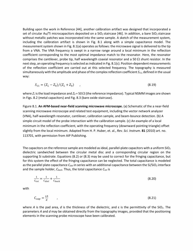
Building upon the work in Reference [44], another calibration artifact was designed that incorporated a set of circular Au/Ti microcapacitors deposited on a SiO2 staircase [46]. In addition, a bare SiO2 staircase without metallic patches was incorporated into the same sample. A sketch of the measurement system, including the calibration artifact is shown in Fig. 8.1 along with a simple capacitance model. The measurement system shown in Fig. 8.1(a) operates as follows: the microwave signal is delivered to the tip from a VNA. The VNA frequency is swept in a narrow range around a local minimum in the reflection coefficient corresponding to the most optimal impedance match to the resonator. Here, the resonator
comprises the cantilever, probe tip, half wavelength coaxial resonator and a 50 shunt resistor. In the next step, an operating frequency is selected as indicated in Fig. 8.1(c). Position-dependent measurements of the reflection coefficient are carried out at this selected frequency. The topography is measured simultaneously with the amplitude and phase of the complex reflection coefficient S11, defined in the usual way:
𝑆11 = (𝑍𝐿 − 𝑍0) (𝑍𝐿 +⁄ 𝑍0) , (8.19)
where ZL is the load impedance and Z0 = 50 (the reference impedance). Typical NSMM images are shown in Figs. 8.2 (metal capacitors) and Fig. 8.3 (bare oxide staircase). Figure 8.1. An AFM-based near-field scanning microwave microscope. (a) Schematic of the a near-field
scanning microwave microscope and related test equipment, including the vector network analyzer
(VNA), half-wavelength resonator, cantilever, calibration sample, and beam-bounce detection. (b) A
simple circuit model of the probe interaction with the calibration sample. (c) An example of a local
minimum in the reflection coefficient, with the operating frequency (downward pointing triangle) offset
slightly from the local minimum. Adapted from H. P. Huber, et. al., Rev. Sci. Instrum. 81 (2010) art. no.
113701, with permission from AIP Publishing.
The capacitors on the reference sample are modeled as ideal, parallel-plate capacitors with a uniform SiO2 dielectric sandwiched between the circular metal disc and a corresponding circular region on the supporting Si substrate. Equations (8.2) or (8.3) may be used to correct for the fringing capacitance, but for this system the effect of the fringing capacitance can be neglected. The total capacitance is modeled as the parallel plate capacitance Cdiel in series with an additional capacitance between the Si/SiO2 interface and the sample holder, Cback. Thus, the total capacitance Ctot is
1
𝐶𝑡𝑜𝑡=
1
𝐶𝑑𝑖𝑒𝑙+
1
𝐶𝑏𝑎𝑐𝑘 (8.20)
with
𝐶𝑐𝑎𝑝 =𝜀𝐴
𝑑 , (8.21)
where A is the pad area, d is the thickness of the dielectric, and ε is the permittivity of the SiO2. The parameters A and d may be obtained directly from the topography images, provided that the positioning elements in the scanning probe microscope have been calibrated.

Figure 8.2. Measurement of microcapacitors with a near-field scanning microwave microscope. (a) Topography and (b) amplitude of the reflection coefficient imaged for a series of oxide-supported, gold microcapacitors. (c) Total capacitance of a series of capacitors, obtained by the calibration procedure outlined in the text. Line cuts taken along the dashed line in (b) provide the raw input for the calibration procedure. Theoretical calculations based on Equations (8.20) and (8.21) are shown as a solid line while data sets are shown as dashed lines. Adapted from H. P. Huber, et. al., Rev. Sci. Instrum. 81 (2010) art. no. 113701, with permission from AIP Publishing. There is an additional parasitic capacitance between the body of the cantilever and the sample surface, which is in parallel to Ctot. The parasitic capacitance can be effectively removed by making a differential measurement:
∆𝑆11 = 𝑆11𝐴𝑢 − 𝑆11
𝑂𝑥 , (8.22)
where 𝑆11𝐴𝑢is the reflection coefficient on the Au/Ti pad and 𝑆11
𝑂𝑥 is the reflection coefficient on an adjacent dielectric oxide surface. It is reasonable assume that the parasitic capacitance is constant across these two positions, as the change in height from the pad to the oxide is much smaller than the total distance from the sample surface to the cantilever body. Figure 8.3. Measurement of a silicon oxide staircase with a near-field scanning microwave microscope [46]. (a) Amplitude of the NSMM reflection coefficient imaged for a bare silicon oxide staircase. The inset shows a line cut along the dashed white line, converted to capacitance following the procedure described in the text. (c) Average capacitance on each step (black dots) compared to the trend predicted by Equation (8.7) (solid grey line). Adapted from H. P. Huber, et. al., Rev. Sci. Instrum. 81 (2010) art. no. 113701, with permission from AIP Publishing. Having accounted for the parasitic capacitance, the magnitude of the relative reflection coefficient |∆𝑆11|can be related to the total capacitance
𝐶𝑡𝑜𝑡 = 𝛼|∆𝑆11| , (8.23) where 𝛼 is a calibration constant in fF/dB. The calculated capacitances for the metal capacitors are shown in Fig. 8.2(c). From the measurements in Fig. 2, the fitted calibration constant is found to be 𝛼=1.5 fF/dB and the background, interfacial capacitance 𝐶𝑏𝑎𝑐𝑘=2 fF. Once again, in order to measure the permittivity of an arbitrary sample, one additional parameter must be found: the effective tip radius. In the present approach, the effective tip radius is obtained from the measurement of the bare dielectric staircase, shown in Fig. 8.3 (Another common method for determination of the effective tip radius is discussed below and is based on atomic force microscope approach curves). We will return to the topic of capacitance calibration based on microcapacitor artifacts in Chapter 11. Though the use of a differential measurement (Equation (8.22)) nominally removes the effects of parasitic capacitances, an alternative is to estimate the parasitic capacitance by retracting the cantilever to a certain distance that is a few micrometers above the sample. The retraction is performed in series of small steps in height h and the reflection coefficient is measured at each step. At a certain distance from the surface, the dependence of the extracted capacitance becomes linear with distance. The slope of the extracted capacitance as a function of height then represents the contribution of the stray capacitance. This can be expressed as
𝐶𝑐𝑎𝑛𝑡 = 𝑘𝑐𝑎𝑛𝑡(ℎ − ℎ0) , (8.24) where the constants kcant and h0 are determined by fitting the linear region of the measured, height-dependent curve with Equation (8.24). The corrected capacitance over the dielectric steps, which accounts for the effects of Ccant in parallel with Ctot, is plotted in Fig. 8.3(b). The effective tip radius may then be determined from Equation (8.7), where contact corresponds to h=0. Additional corrections may be made for fringe capacitance contributions in the form of Equation (8.2) or Equation (8.3). Though this calibration procedure can be applied in many areas, it does not address measurements of loss or non-capacitive reactance. In addition, the procedure requires a number of micro-fabricated capacitance standards that may contribute additional uncertainty to the measurement. Introducing an alternative approach based on one-port calibration of network analyzers reduces the number of required standards and provide full quantitative determination of both resistive and reactive parts of the local impedance [47]. As above, this procedure assumes that the NSMM operates in contact mode. As in one-port calibration of guided wave systems, the definition of the calibration reference plane is an important consideration (see Chapter 2). Here, it is possible to define the reference plane either at the probe tip or at another location in the signal path, as will be discussed later. From Chapter 2, recall that in a three-term error model, the measured, raw reflection coefficient S11m is related the corrected reflection coefficient S11 through
𝑆11 =𝑆11𝑚−𝑒00
𝑒01+𝑒11(𝑆11𝑚−𝑒00) , (8.25)
where the error coefficients are defined as follows: e00 is directivity, the product e10e01 is tracking and e11 is the port match. From the measurements of three electrically distinct standards with known reflection coefficients, it is possible to calculate the complex error coefficients. Once the values of the error coefficients are known, the real and imaginary parts of the impedance at the reference plane can be determined from the corrected reflection coefficient via Equation (8.19). The reference impedance Z0 can
be chosen arbitrarily. In Reference [47], the reference impedance was chosen to be 10 k and three capacitors from the calibration artifacts described above were chosen as standards. This approach provides calibrated, local measurements of complex impedance by use of NSMMs, but it has a relatively large uncertainty, particularly for small capacitance measurements, and the procedure is not transferable from the calibration substrate to an arbitrary sample. The relatively large uncertainty arises from the difficulty in estimation of the change in fringing electromagnetic fields around the tip when moved from calibration standards to the sample under test. The problem of transfer from the calibration substrate to an arbitrary sample was solved by Gramse, et al. [30]. Their approach builds on the initial calibration ideas of Hoffman, et. al. in Reference [47] and Farina et al. in Reference [48]. In the latter reference, one central idea was the variation of the probe-sample distance to create different calibration “standards.” The Gramse approach works in situ directly on the sample under test and does not require a special calibration sample [30]. The particular innovation in the approach is to simultaneously perform an NSMM measurement with a low-frequency electrostatic capacitance measurement as the tip approaches the sample. Though no longer necessary for calibration, well-characterized samples and substrates remain useful for validation of the procedure and for systematic study of effective tip radii on different classes of samples. The calibration procedure presented in Reference [30] works in typical NSMM operating frequency ranges (about 1 GHz to 26 GHz) and takes into account the full test platform response, including the VNA, cabling, and the specific geometry of the

tip-sample interaction area. Because this approach may become a widely-used procedure for NSMM calibration, we describe the steps of this method in greater detail below. Our description will assume a measurement system similar to that shown in Fig. 8.1(a), but it is straightforward to adapt the procedure to other configurations.
In the first step, the measured, complex reflection coefficient is converted into a complex impedance (admittance). Next, a one-port calibration is applied [47], following Equation (8.25). The reference plane is chosen to be right behind the cantilever chip shown in Fig. 8.1(a). This choice of reference plane means that the measured DUT includes the body of cantilever and the tip-sample system. As discussed in Chapter 2, this choice is arbitrary, but has direct consequences for the implementation and interpretation of the de-embedding procedure. This choice of reference plane was necessitated by complications encountered in Reference [47] arising from the dependence of the stray capacitance of the cantilever chip upon the probe-sample distance. These complications may also reflect the fact that the probe tip does not fulfill the condition for single mode propagation at the reference plane. Strictly speaking, this precludes a definition of the reference plane at the probe tip. Note that this problem is significantly mitigated for conducting or highly planar samples. The mapping of the raw measured 𝑆11𝑚 onto corrected S11 is the same as in the previous case, with three complex error coefficients that have to be determined from the measurement of at least three reference samples with known impedances. However, this requires the positioning of these reference samples at the calibration reference plane. For the given choice of the reference plane, this represents a challenge. However, this problem is also addressed by utilizing a height-dependent measurement of the reflection coefficient in conjunction with an electrostatic force measurement. Specifically, the amplitude and phase of the reflection coefficient 𝑆11𝑚 is measured as a function of the tip-sample distance h at a fixed, selected frequency. For metallic and purely dielectric substrates, the character of the impedance change is purely capacitive, which allows the simultaneous, low-frequency measurement of the electrostatic force. As in electrostatic force microscopy (EFM), the force is proportional to 𝑑𝐶/𝑑ℎ: [23]-[25]
𝐹𝑒𝑠(ℎ) =1
4
𝑑𝐶
𝑑ℎ𝑉02 cos(2𝜔𝑡) →
𝑑𝐶
𝑑ℎ=
2𝐹𝑒𝑠,2𝜔
𝑉02 , (8.26)
where V0 is the amplitude of low frequency modulation voltage and ω is the modulation frequency. Integrating the measured Fes(h) curves gives the desired tip-surface capacitance and the corresponding admittance 𝑌(ℎ) = 𝑗2𝜋𝑓𝐶(ℎ). This admittance acts as the reference sample in place of a calibration artifact and serves as the input into the mapping equation from the measured to the corrected reflection coefficient. Since this creates an overdetermined system (assuming that the measurements are made at more than three heights), an optimization algorithm is used to solve equation (8.25) for the error coefficients. It is important to recognize that dC/dh in Equation (8.26) may have to be adjusted by a small offset to account for the stray capacitance that is not detected by EFM. This EFM-based calibration procedure has been verified across multiple operating frequencies [30]. Having calibrated the S11 reflection coefficients, the S11 images can be converted into the real and imaginary parts of impedance or admittance. Once again, to extract parameters of interest from calibrated reflection coefficient measurements of an arbitrary sample, it is necessary to know the effective tip geometry. Fortunately, the approach curve measurements enable the extraction of the tip geometry such as radius R, cone angle𝜃, and cone height L by comparison of the calibrated measurements to finite element simulations. In some cases, the cone height and cone angle may be fixed to manufacturers’ nominal values, thus reducing the set of fitting parameters in the determination of tip geometry and
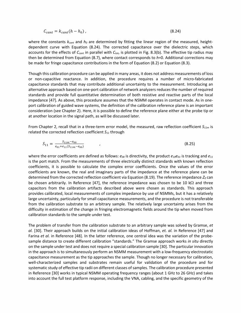
parasitic capacitance. These parameters are in general considered to be effective dimensions, absorbing the influence of any imperfect approximations or unknown electromagnetic field interactions. Finally, a thorough characterization of an NSMM system has been described in Reference [49], including the introduction of a calibration approach for spatially-resolved, subsurface measurements as a function of material and sample depth. Although the spatial resolution was in the micrometer range the results are in principle scalable to nanometer dimensions. The approach was designed for a critically coupled resonator system. As with many NSMMs, the probe’s interaction with the sample leads to changes in the resonance frequency and the quality factor, which manifest as changes in the complex reflection coefficient. A schematic circuit model of the critically coupled resonator and the sample impedance is shown in Fig. 8.4. The schematic also shows the reference plane at the input to the resonator (P1) and at the base of the cantilever (P2). At the P1 reference plane, a standard coaxial or waveguide calibration is performed. To translate to the next reference plane P2, it is necessary to de-embed the resonator between P1 and P2. This can be accomplished through a frequency-swept measurement of the reflection coefficient when the tip is far from the surface of the sample. From this frequency sweep, the circuit parameters of the resonator in the vicinity of the operating frequency can be established. Having established these circuit parameters, the resonator can be de-embedded and the reference plane can be moved to P2 to get the calibrated probe-sample coupling impedance. Figure 8.4. Critically coupled resonator and sample impedance. Reference plane P1 is at the input to
the resonator and reference plane P2 is at the tip of the probe. The sample resistance RS and sample
capacitance CS contribute to the overall sample impedance ZS. © [year] IEEE. Adapted, with permission
from Jonathan D. Chisum, and Zoya Popović, IEEE Trans. Microw. Theory Techn. 60 (2012) pp.2605-2015.
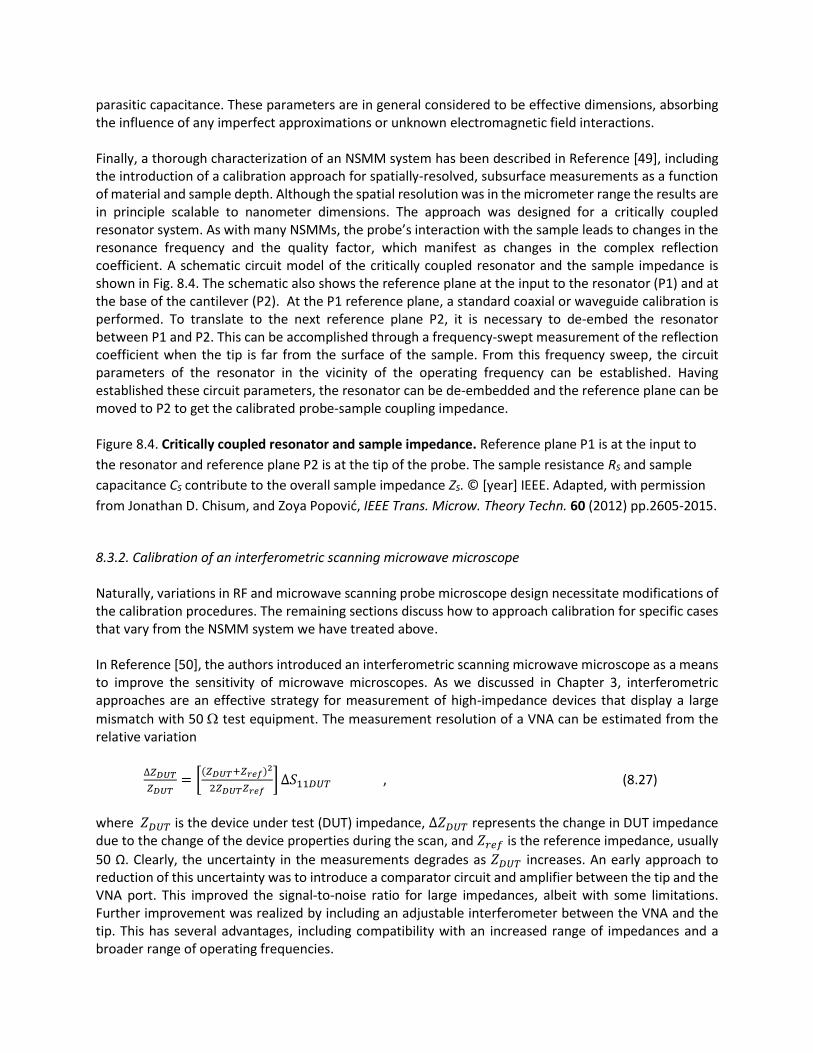
8.3.2. Calibration of an interferometric scanning microwave microscope Naturally, variations in RF and microwave scanning probe microscope design necessitate modifications of the calibration procedures. The remaining sections discuss how to approach calibration for specific cases that vary from the NSMM system we have treated above. In Reference [50], the authors introduced an interferometric scanning microwave microscope as a means to improve the sensitivity of microwave microscopes. As we discussed in Chapter 3, interferometric approaches are an effective strategy for measurement of high-impedance devices that display a large
mismatch with 50 test equipment. The measurement resolution of a VNA can be estimated from the relative variation
∆𝑍𝐷𝑈𝑇
𝑍𝐷𝑈𝑇= [
(𝑍𝐷𝑈𝑇+𝑍𝑟𝑒𝑓)2
2𝑍𝐷𝑈𝑇𝑍𝑟𝑒𝑓] ∆𝑆11𝐷𝑈𝑇 , (8.27)
where 𝑍𝐷𝑈𝑇 is the device under test (DUT) impedance, ∆𝑍𝐷𝑈𝑇 represents the change in DUT impedance due to the change of the device properties during the scan, and 𝑍𝑟𝑒𝑓 is the reference impedance, usually
50 Ω. Clearly, the uncertainty in the measurements degrades as 𝑍𝐷𝑈𝑇 increases. An early approach to reduction of this uncertainty was to introduce a comparator circuit and amplifier between the tip and the VNA port. This improved the signal-to-noise ratio for large impedances, albeit with some limitations. Further improvement was realized by including an adjustable interferometer between the VNA and the tip. This has several advantages, including compatibility with an increased range of impedances and a broader range of operating frequencies.

Figure 8.5 Interferometric scanning microwave microscope. Schematic of the circuit and test platform
for implementing an interferometric scanning microwave microscope NSMM. The interferometric
measurement is made by use of a vector network analyzer (VNA). Reprinted from T. Dargent, K. Haddadi,
T. Lasri, N. Clement, D. Ducatteeau, B. Legrand, H. Tanbakuchi, and D. Theron, Rev. Sci. Instrum. 84 (2013)
art. no. 123705, with permission from AIP Publishing.
The interferometer connection to the VNA is shown in Fig. 8.5. This is once again a single port measurement. The signal from the source is split and directed through an interferometer that resembles a Mach-Zehnder configuration. The interferometer comprises a coaxial power divider and two hybrid couplers, one of which is connected to an attenuator. The signal from the source at port 1 of the VNA (a1 in Fig. 8.5) is split in the power divider and one arm is fed to the tip of the microscope (ainc). The reflected signal from the tip-sample system (aref) is combined with the second part of the signal passing through the attenuator in the second coupler. The resulting interferometric signal is then amplified and analyzed in the receiver in port 1 of the VNA. The attenuator is adjusted to cancel the signal a3 in front of the amplifier through destructive interference between the two branches of the interferometer. The variable attenuator ensures that complete cancellation through interference can be obtained for any impedance values. This case represents an easily implemented improvement to the signal-to-noise ratio of NSMMs. However, use of the interferometer configuration requires a modified calibration procedure; a traditional, single port calibration procedure is not sufficient. Although the whole assembly of the interferometer and the tip-sample junction is connected to a single port of the VNA, the calibration has to be done between the port 1 source of the VNA through the assembly to the receiver of the port 1. To circumvent this, a calibration procedure based on a modified one-port error model was developed for interferometric NSMM. A set of oxide microcapacitors similar to those described earlier may serve as reference standards for the interferometer calibration. The calibration is carried out as follows. The reference load with reflection coefficient S11ref is obtained by positioning the tip onto a thick dielectric that serves to establish the reference impedance. The attenuator is set to minimize the interference signal such that at a given frequency the transmission signal (a3) is close to zero, thus ensuring high measurement sensitivity for impedances around the reference impedance. As shown in Fig. 8.5, a4 represents the incoming signal from the DUT into the VNA. One can consider this as a signal entering a second port, an effective “port 2,” loaded with the reflection coefficient of sample under test. Thus, it is possible to represent the effect of the interferometer as a matrix complex scattering parameters resembling a two-port error box. It is possible to relate the measured reflection coefficient in terms of the scattering parameters of the interferometer through Equation (8.25), provided that the 𝑒𝑖𝑗
coefficients now represent the 𝑆𝑖𝑗 parameters of the interferometer with indices equal to 0 replaced by 1
and indices equal to 1 replaced by 2. S11 represents the calibration impedance reflection coefficient. These parameters as “interferometer transition coefficients.” The interferometer transition coefficients are determined from measurements of three known standards chosen from a calibration kit. Increasing the number of calibration standards leads to an overdetermined system and in turn, a more robust calibration with reduced statistical uncertainty. If the calibration standards are all pure capacitors, it is possible to reduce the complexity of numerical optimization by assuming that only the phase shift of the reflection coefficient has to be taken into account.
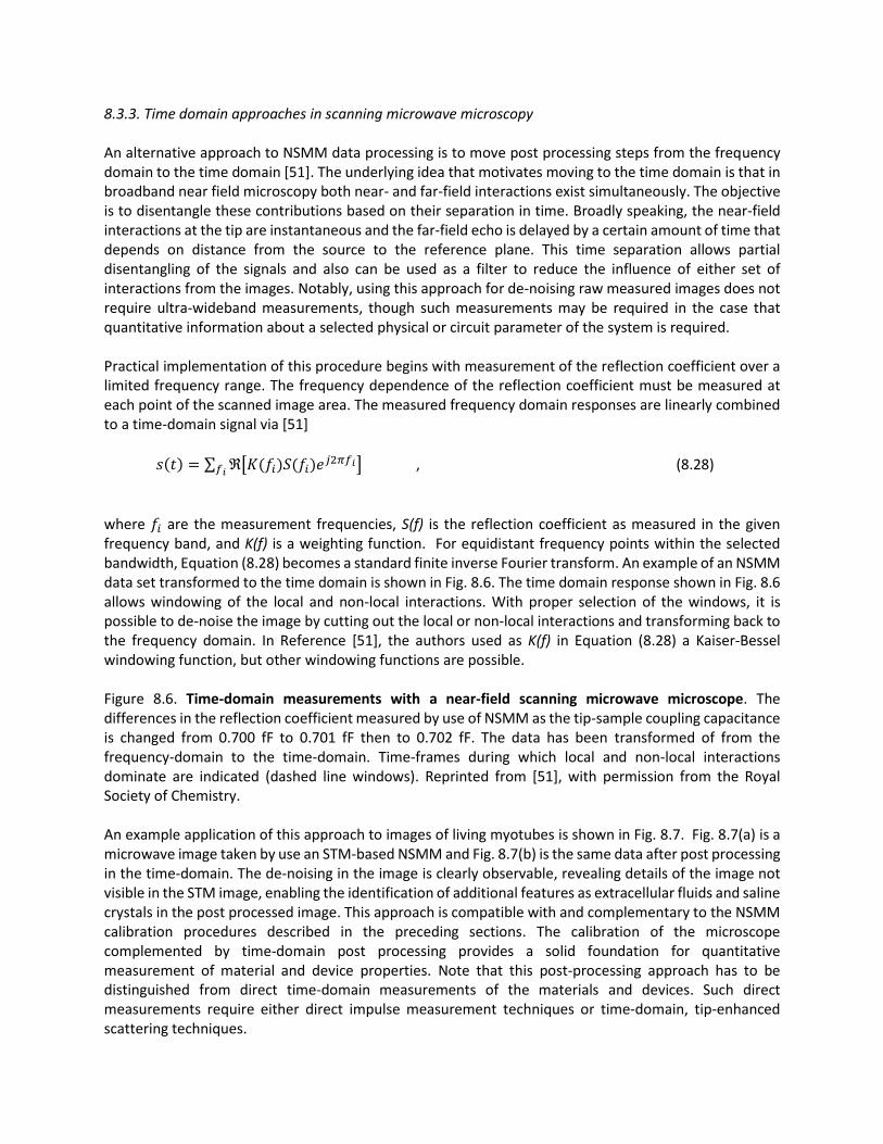
8.3.3. Time domain approaches in scanning microwave microscopy An alternative approach to NSMM data processing is to move post processing steps from the frequency domain to the time domain [51]. The underlying idea that motivates moving to the time domain is that in broadband near field microscopy both near- and far-field interactions exist simultaneously. The objective is to disentangle these contributions based on their separation in time. Broadly speaking, the near-field interactions at the tip are instantaneous and the far-field echo is delayed by a certain amount of time that depends on distance from the source to the reference plane. This time separation allows partial disentangling of the signals and also can be used as a filter to reduce the influence of either set of interactions from the images. Notably, using this approach for de-noising raw measured images does not require ultra-wideband measurements, though such measurements may be required in the case that quantitative information about a selected physical or circuit parameter of the system is required. Practical implementation of this procedure begins with measurement of the reflection coefficient over a limited frequency range. The frequency dependence of the reflection coefficient must be measured at each point of the scanned image area. The measured frequency domain responses are linearly combined to a time-domain signal via [51]
𝑠(𝑡) = ∑ ℜ[𝐾(𝑓𝑖)𝑆(𝑓𝑖)𝑒𝑗2𝜋𝑓𝑖]𝑓𝑖 , (8.28)
where 𝑓𝑖 are the measurement frequencies, S(f) is the reflection coefficient as measured in the given frequency band, and K(f) is a weighting function. For equidistant frequency points within the selected bandwidth, Equation (8.28) becomes a standard finite inverse Fourier transform. An example of an NSMM data set transformed to the time domain is shown in Fig. 8.6. The time domain response shown in Fig. 8.6 allows windowing of the local and non-local interactions. With proper selection of the windows, it is possible to de-noise the image by cutting out the local or non-local interactions and transforming back to the frequency domain. In Reference [51], the authors used as K(f) in Equation (8.28) a Kaiser-Bessel windowing function, but other windowing functions are possible. Figure 8.6. Time-domain measurements with a near-field scanning microwave microscope. The differences in the reflection coefficient measured by use of NSMM as the tip-sample coupling capacitance is changed from 0.700 fF to 0.701 fF then to 0.702 fF. The data has been transformed of from the frequency-domain to the time-domain. Time-frames during which local and non-local interactions dominate are indicated (dashed line windows). Reprinted from [51], with permission from the Royal Society of Chemistry. An example application of this approach to images of living myotubes is shown in Fig. 8.7. Fig. 8.7(a) is a microwave image taken by use an STM-based NSMM and Fig. 8.7(b) is the same data after post processing in the time-domain. The de-noising in the image is clearly observable, revealing details of the image not visible in the STM image, enabling the identification of additional features as extracellular fluids and saline crystals in the post processed image. This approach is compatible with and complementary to the NSMM calibration procedures described in the preceding sections. The calibration of the microscope complemented by time-domain post processing provides a solid foundation for quantitative measurement of material and device properties. Note that this post-processing approach has to be distinguished from direct time-domain measurements of the materials and devices. Such direct measurements require either direct impulse measurement techniques or time-domain, tip-enhanced scattering techniques.
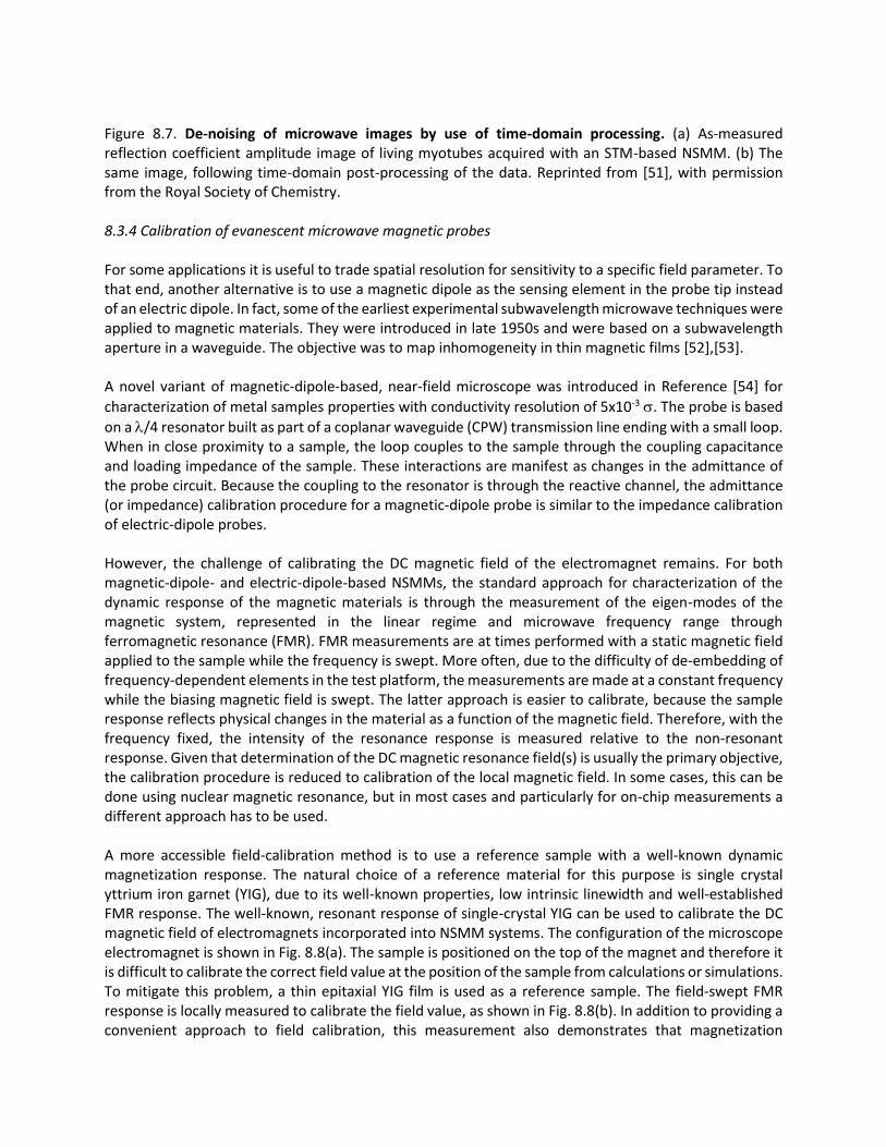
Figure 8.7. De-noising of microwave images by use of time-domain processing. (a) As-measured reflection coefficient amplitude image of living myotubes acquired with an STM-based NSMM. (b) The same image, following time-domain post-processing of the data. Reprinted from [51], with permission from the Royal Society of Chemistry. 8.3.4 Calibration of evanescent microwave magnetic probes For some applications it is useful to trade spatial resolution for sensitivity to a specific field parameter. To that end, another alternative is to use a magnetic dipole as the sensing element in the probe tip instead of an electric dipole. In fact, some of the earliest experimental subwavelength microwave techniques were applied to magnetic materials. They were introduced in late 1950s and were based on a subwavelength aperture in a waveguide. The objective was to map inhomogeneity in thin magnetic films [52],[53]. A novel variant of magnetic-dipole-based, near-field microscope was introduced in Reference [54] for
characterization of metal samples properties with conductivity resolution of 5x10⁻³ . The probe is based
on a /4 resonator built as part of a coplanar waveguide (CPW) transmission line ending with a small loop. When in close proximity to a sample, the loop couples to the sample through the coupling capacitance and loading impedance of the sample. These interactions are manifest as changes in the admittance of the probe circuit. Because the coupling to the resonator is through the reactive channel, the admittance (or impedance) calibration procedure for a magnetic-dipole probe is similar to the impedance calibration of electric-dipole probes. However, the challenge of calibrating the DC magnetic field of the electromagnet remains. For both magnetic-dipole- and electric-dipole-based NSMMs, the standard approach for characterization of the dynamic response of the magnetic materials is through the measurement of the eigen-modes of the magnetic system, represented in the linear regime and microwave frequency range through ferromagnetic resonance (FMR). FMR measurements are at times performed with a static magnetic field applied to the sample while the frequency is swept. More often, due to the difficulty of de-embedding of frequency-dependent elements in the test platform, the measurements are made at a constant frequency while the biasing magnetic field is swept. The latter approach is easier to calibrate, because the sample response reflects physical changes in the material as a function of the magnetic field. Therefore, with the frequency fixed, the intensity of the resonance response is measured relative to the non-resonant response. Given that determination of the DC magnetic resonance field(s) is usually the primary objective, the calibration procedure is reduced to calibration of the local magnetic field. In some cases, this can be done using nuclear magnetic resonance, but in most cases and particularly for on-chip measurements a different approach has to be used. A more accessible field-calibration method is to use a reference sample with a well-known dynamic magnetization response. The natural choice of a reference material for this purpose is single crystal yttrium iron garnet (YIG), due to its well-known properties, low intrinsic linewidth and well-established FMR response. The well-known, resonant response of single-crystal YIG can be used to calibrate the DC magnetic field of electromagnets incorporated into NSMM systems. The configuration of the microscope electromagnet is shown in Fig. 8.8(a). The sample is positioned on the top of the magnet and therefore it is difficult to calibrate the correct field value at the position of the sample from calculations or simulations. To mitigate this problem, a thin epitaxial YIG film is used as a reference sample. The field-swept FMR response is locally measured to calibrate the field value, as shown in Fig. 8.8(b). In addition to providing a convenient approach to field calibration, this measurement also demonstrates that magnetization

dynamics can be measured with an electric dipole NSMM. The position of the resonances in the field-swept FMR measurement at constant applied RF frequency determines the DC resonant fields. As the field-dependent resonance frequencies for YIG are well known, the position of the dip in the curve calibrates the field value for a given probe position. Also note that each resonance dip corresponds to an excited spin wave mode in the magnetic sample. Therefore, the measured dip(s) represent dynamic excitations of the measured sample. Thus, by selecting the corresponding DC field of an excited mode and scanning over the sample, one can visualize the spin wave pattern for a selected mode [55]. Figure 8.8 Near-field scanning microwave measurements of an Yttrium Iron Garnet (YIG) film. (a) Photograph of an electromagnet and RF signal path integrated into the sample holder for use with a commercial broadband scanning microwave microscope. (b) Amplitude of the local, reflected signal from a YIG thin film measured with an NSMM operating at a constant frequency. 8.3.5. Evanescent microwave microscopes in transmission mode Recently, some efforts in scanning microwave microscopy have moved to the implementation of microscopes in transmission mode rather than reflection mode. This trend is particularly important for nondestructive subsurface tomography of defects and interfaces. An early report of such an effort appeared in Reference [56], in which the feasibility of using an NSMM in transmission mode was investigated by use of three-dimensional, finite-element modeling. A sensitivity analysis was carried out by varying different parameters of the system including the measurement frequency and observing the resultant change in the complex transmission coefficient. The models are supported by preliminary measurements on a Si substrate with spatially-varying dopant concentrations. The investigation concluded that measurement of transmission provides improved sensitivity with respect to existing reflection-mode NSMMs, especially for the phase. This improved sensitivity has important experimental implications, but at present it comes at the price of quantitative metrology. A well-established calibration procedure for a transmission mode NSMM does not presently exist. A further complication is that the traditional, two-port VNA calibration procedures are not directly transferable to this case. One significant challenge is the establishment of the reference planes. On one side of the sample, the reference plane can be chosen in a similar way to the case of a single port calibration at the probe tip. On the other side, the plane can be chosen to be at a designated port, probe, or second electric dipole (antenna). However, the device now includes not only the tip-sample assembly of the first port, but also the transmission coupling for the second port as well as the complex interaction of the microwaves throughout the thickness of sample. Thus, the total DUT is a complicated, multifaceted system and it is extremely challenging to de-embed the material properties from the total DUT measurement. Furthermore, neither the probe tip nor the second antenna fulfills the conditions for single mode propagation at the reference plane. Moving forward, the establishment of the necessary error model and error coefficients for a transmission-mode NSMM is formidable. Possible ways forward include the multimode calibration procedure discussed in Chapter 2 or procedures for calibration of antenna-to-antenna transmission in the near field [57]. This is not a simple problem and the work in this area is ongoing.
References [1] M. Fee, S. Chu, and T. W. Hänsch, “Scanning electromagnetic transmission line microscope with subwavelength resolution,” Optics Communications 69 (1989) pp. 219–224. [2] D. E. Steinhauer, C. P. Vlahacos, C. Canedy, A. Stanishevsky, R. Melngailis, R. Ramesh, F. C. Wellstood, and S. M. Anlage, “Imaging of microwave permittivity, tunability, and damage recovery in (Ba,Sr)TiO3 thin films,” Applied Physics Letters 75 (1999) pp. 3180-3182. [3] M. Tabib-Azar, N. Shoemaker, and S. Harris, “Nondestructive characterization of materials by evanescent microwaves,” Measurement Science and Technology 4 (1993) pp. 583–590. [4] M. M. Wang, K. Haddadi, D. Glay, and T. Lasri, “Compact near field microwave microscope based on the multi-port technique,” Proceedings of the 40th European Microwave Conference (Paris, 2010) pp. 771–774. [5] M. Golosovsky and D. Davidov, “Novel mm-wave near-field resistivity microscope,” Applied Physics Letters 68 (1996) pp. 1579–1581. [6] V. V. Talanov and A. R. Schwartz, “Near-field scanning microwave microscope for interline capacitance characterization of nanoelectronics interconnect,” IEEE Transactions on Microwave Theory and Techniques 57 (2009) pp. 1224–1229. [7] C. Gao and X.-D. Xiang, “Quantitative microwave near-field microscopy of dielectric properties,” Review of Scientific Instruments 69 (1998) pp. 3846–3851. [8] S. J. Stranick and P. S. Weiss, “A versatile microwave frequency-compatible scanning tunneling microscope” Review of Scientific Instruments 64 (1993) pp. 1232–1234. [9] M. Tabib-Azar and Y. Wang, “Design and fabrication of scanning near-field microwave probes compatible with atomic force microscopy to image embedded microstructures,“ IEEE Transactions on Microwave Theory and Techniques 52 (2004) pp. 971–979. [10] K. Lai, W. Kundhikanjana, M. Kelly, and Z. X. Shen, “Modeling and characterization of cantilever-based near-field scanning microwave impedance microscope,” Review of Scientific Instruments 79 (2008) art. no. 063703. [11] B. T. Rosner and D. W. van der Weide, “High-frequency near-field microscopy,” Review of Scientific Instruments 73 (2002) pp. 2505–2525. [12] S.M. Anlage, V. V. Talanov, and A. R. Schwartz, “Principles of near-field microscope,” in Scanning Probe Microscopy, S. Kalinin, and A. Gruverman, Eds. (Springer, 2007) pp. 215-253. [13] M. J. Yoo, T. A. Fulton, H. F. Hess, R. L. Willet, L. N. Dunkleberger, R.J. Chichester, L. N. Pfeiffer, and K. W. West, “Scanning Single-Electron Transistor Microscopy: Imaging Individual Charges,” Science 276 (1997) pp. 579-582. [14] G. J. Sloggett, N. G. Barton, and S. J. Spencer, “Fringing fields in disc capacitors,” Journal of Physics A: Mathematical and General 19 (1986) pp. 2725-2736. [15] W. R. Smythe, Static and Dynamic Electricity (McGraw-Hill, 1950). [16] H. P. Kleinknecht, J. R. Sandercock, and H. Meier, “An experimental scanning capacitance microscope,” Scanning Microscopy 2 (1988) pp. 1839-1844. [17] C. Gao, F. Duewer, and X.-D. Xiang, “Quantitative microwave evanescent microscopy,” Applied Physics Letters 75 (1999) pp. 3005-3007. [18] S. V. Kalinin, E. Karapetian, M. Kachanov, “Nanoelectromechanics of piezoresponse force microscopy,” Physical Review B 70 (2004) art. no. 184101. [19] E. A. Eliseev, S. V. Kalinin, S. Jesse, S. L. Bravina, A. N. Morozovska, “Electromechanical Detection in Scanning Probe Microscopy: Tip Models and Materials Contrast,” Journal of Applied Physics 102 (2007) art. no. 014109.

[20] B. M. Law and F. Rieutord, “Electrostatic forces in atomic force microscopy,” Physical Review B 66 (2002) art. no. 035402. [21] G. M. Sacha, E. Sahagun, and J. J. Saenz, “A method for calculating capacitances and electrostatic forces in atomic force microscopy,” Journal of Applied Physics 101 (2007) art. no. 024310. [22] G. M. Sacha, “Method to calculate electric fields at very small tip-sample distances in atomic force microscopy,” Applied Physics Letters 97 (2010) art. no. 033115. [23] S. Gomez-Monivas, J. J. Saenz, R. Carminati, and J. J. Greffet, “Theory of electrostatic probe microscopy: A simple perturbative approach,” Applied Physics Letters 76 (2000) pp. 2955-2957. [24] B. M. Law and F. Rieutord, “Electrostatic forces in atomic force microscopy,” Physical Review B 66 (2002) art. no. 035402. [25] S. Hudlet, M. Saint Jeana, C. Guthmann, and J. Berger, “Evaluation of the capacitive force between an atomic force microscopy tip and a metallic surface,” European Physical Journal B 2 (1998) pp. 5-10. [26] G. Gomila, J. Toset, and L. Fumagalli, “Nanoscale capacitance microscopy of thin dielectric films,” Journal of Applied Physics 104 (2008) art. no. 024315. [27] Š. Lanyi, “Effect of tip shape on capacitance determination accuracy in scanning capacitance microscopy,” Ultramicroscopy 103 (2005) pp. 221-228. [28] Sˇ. Lanyi, “Shape dependence of the capacitance of scanning capacitance microscope probes.” Ultramicroscopy 108 (2008) pp.712-717. [29] G. Gomila, G. Gramse, L. Fumagalli,“ Finite size effects and analytical modeling of electrostatic force microscopy applied to dielectric films,” Nanotechnology 25 (2014) art. no. 255702. [30] G. Gramse, M. Kasper, L. Fumagalli, G. Gomila, P. Hinterdorfer and F. Kienberger,” Calibrated complex impedance and permittivity measurements with scanning microwave microscopy,” Nanotechnology 26 (2015) art. no. 149501. [31] Y. Naitou, A. Yasaka, and N. Ookubo, “An analytical model for capacitance between probe tip and dielectric film deduced by high frequency electromagnetic field simulations,” Journal of Applied Physics 105 (2009) art. no. 044311. [32] A. Sommerfeld, “Über die Ausbreitung der Wellen in der drahtlosen Telegraphie,” Annalen der Physik 28 (1909) pp. 665–736. [33] A. Sommerfeld, “Über die Ausbreitung der Wellen in der drahtlosen Telegraphie,” Annalen der Physik 81 (1926) pp. 1135–1153. [34] E. F. Kuester and D. C. Chang, “Evaluation of Sommerfeld integrals associated with dipole sources above earth,” Electromagnetics Laboratory/The MIMICAD Research Center (1979) Paper 65. [35] R. W. P. King, Theory of linear antennas, (Harvard University Press, 1956). [36] L. B. Felsen and N. Marcuvitz, Radiation and Scattering of Waves (IEEE Press, 1994). [37] J. R. Wait, ElectromagneticWaves in Stratified Media (IEEE Press, 1996). [38] I. V. Lindell and E. Alanen, “Exact image theory for the Sommerfeld half-space problem, Part I: Vertical magnetic dipole,” IEEE Transactions on Antennas and Propagation 32 (1984) pp. 126-133. [39] I. V. Lindell and E. Alanen, Exact Image Theory for Sommerfeld Half-Space Problem, Part II: Vertical Electric Dipole,” IEEE Transactions on Antennas and Propagation 32 (1984) pp.841-847. [40] J. R. Wait, “Possible influence of the ionosphere on the impedance of a ground-based antenna,” Journal of Research of the National Bureau of Standards-D 66 (1962) pp. 563-569. [41] J. R. Wait, “Impedance characteristics of electric dipoles over a conducting half-space,” Radio Science 4 (1969) p 971. [42] E. Alanen and I. Lindell, “Impedance of vertical electric and magnetic dipole above a dissipative ground,” Radio Science 19 (1984) pp. 1469-1474. [43] L. E. Vogler and J. L. Noble, “Curves of input impedance change due to ground for diploe antennas,” National Bureau of Standards (1964) Monograph 72.

[44] A. Karbassi, D. Ruf, A. D. Bettermann, C. A. Paulson, D. W. van der Weide, H. Tanbakuchi, and R. Stancliff, “Quantitative scanning near field microwave microscopy for thin film dielectric constant measurement,” Review of Scientific Instruments 79 (2008) art. no. 094706. [45] M. Tabib-Azar, P. S. Pathak, G. Ponchak, and S. LeClair, “Nondestructive superresolution imaging of defects and nonuniformities in metals, semiconductors, dielectrics, composites, and plants using evanescent microwaves,” Review of Scientific Instruments 70 (1999) pp. 2783-2792. [46] H. P. Huber, M. Moertelmaier, T. M. Wallis, C. J. Chiang, M. Hochleitner, A. Imtiaz, Y. J. Oh, K. Schilcher, M. Dieudonne, J. Smoliner, P. Hinterdorfer, S. J. Rosner, H. Tanbakuchi, P. Kabos and F. Kienberger, “Calibrated nanoscale capacitance measurements using a scanning microwave microscope,” Review of Scientific Instruments 81 (2010) art. no. 113701. [47] J. Hoffmann, M. Wollensack, M. Zeier, J. Niegemann, H-P. Huber and F. Kienberger, “A calibration algorithm for near field, scanning microwave microscopes,” Proceedings of the 2012 12th IEEE International conference on nanotechnology (Birmingham, 2012). [48] M. Farina, D. Mencarelli, A. Di Donato, G. Venanzoni, and A. Morini, “Calibration Protocol for Broadband Near-Field Microwave Microscopy,” IEEE Transactions on Microwave Theory and Techniques 59 (2011) pp. 2769-2776. [49] J. D. Chisum, and Z. Popović, “Performance Limitations and Measurement Analysis of a Near-Field Microwave Microscope for Nondestructive and Subsurface Detection,” IEEE Transactions on Microwave Theory and Techniques 60 (2012) pp.2605-2015. [50] T. Dargent, K. Haddadi, T. Lasri, N. Clement, D. Ducatteeau, B. Legrand, H. Tanbakuchi, and D. Theron, “An interferometric scanning microwave microscope and calibration method for sub-fF microwave measurements,” Review of Scientific Instruments 84 (2013) art. no. 123705. [51] M. Farina, A. Lucesoli, T. Pietrangelo, A. di Donato, S. Fabiani, G. Venanzoni, D. Mencarelli, T. Rozzia and A. Morinia, “Disentangling time in a near-field approach to scanning probe microscopy,” Nanoscale 3 (2011) pp. 3589-3593. [52] Z. Frait, V. Kambersky, Z. Malek, and M. Ondris, “Local variations of uniaxial anisotropy in thin films,” Czechoslovak Journal of Physics 10 (1960) p. 616. [53] R. F. Soohoo, Microwave Magnetics (Harper & Row, 1985). [54] R. Wang, F. Li, and M. Tabib-Azar, “Calibration methods of a 2 GHz evanescent microwave magnetic probe for noncontact and nondestructive metal characterization for corrosion, defects, conductivity, and thickness nonuniformities,” Review of Scientific Instruments 76 (2005) art. no. 054701. [55] T. An, N. Ohnishi, T. Eguchi, Y. Hasegawa, and P, Kabos, “Local excitation of ferromagnetic resonance and its spatially resolved detection with an open-ended radio-frequency probe,” IEEE Magnetics Letters 1 (2010) art. no. 3500104. [56] A. O. Oladipo, A. Lucibello, M. Kasper, S. Lavdas, G. M. Sardi, E. Proietti, F. Kienberger, R. Marcelli, and N. C. Panoiu,” Analysis of a transmission mode scanning microwave microscope for subsurface imaging at the nanoscale” Applied Physics Letters 105 (2014) art. no. 133112. [57] D. M. Kerns, ”Plane-wave scattering matrix theory of antennas and antenna-antenna interactions,” National Bureau of Standards (1981) Monograph 162.

LO LO
(a)
(b) (c)
Figure 8.1
Cdiel
Cback
Ccant
resonator
50W
A/D A/D
B A
VNA
2.17 2.18Frequency (GHz)
S
(d
B)
11
10
0
-10


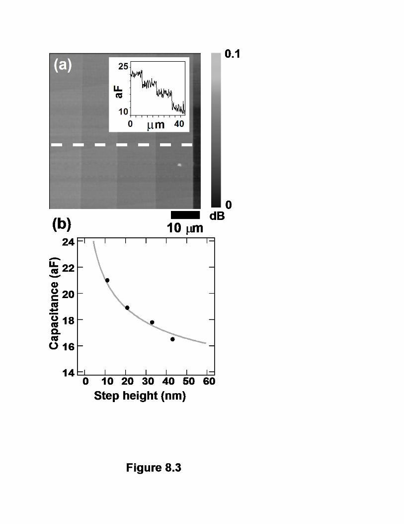

Figure 8.5
VNA

Figure 8.6
(a) (b)
Figure 8.7

(a)
Figure 8.8
(b)


![IEC 62209-3 Vector Probe-Array SAR Measurement 62209-3 Vector Probe-Array SAR Measurement MIC MRA International Workshop 2016 ... [Merckel, Joisel, Bolomey, Proc. AMTA, 2003], [Cozza,](https://img.pdfslide.us/doc/110x75/5aed901f7f8b9a6625901def/iec-62209-3-vector-probe-array-sar-62209-3-vector-probe-array-sar-measurement-mic.jpg)