Embed Size (px)
Citation preview

3/12/2019
1
1
Chapter 6 Physics of MOS Transistors
6.1 Structure of MOSFET
6.2 Operation of MOSFET
6.3 MOS Device Models
6.4 PMOS Transistor
6.5 CMOS Technology
6.6 Comparison of Bipolar and CMOS Devices
CH 6 Physics of MOS Transistors 2
Chapter Outline
3/12/2019
2
CH 6 Physics of MOS Transistors 3
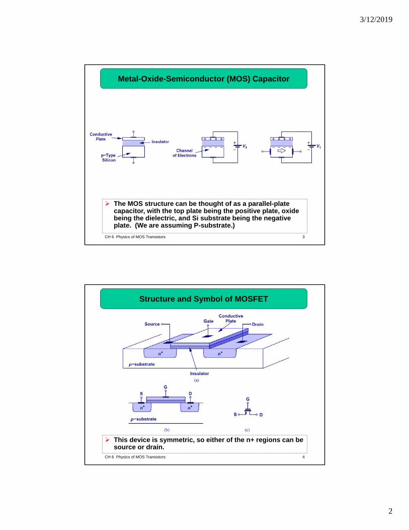
Metal-Oxide-Semiconductor (MOS) Capacitor
The MOS structure can be thought of as a parallel-plate capacitor, with the top plate being the positive plate, oxide being the dielectric, and Si substrate being the negative plate. (We are assuming P-substrate.)
CH 6 Physics of MOS Transistors 4
Structure and Symbol of MOSFET
This device is symmetric, so either of the n+ regions can be source or drain.
3/12/2019
3
CH 6 Physics of MOS Transistors 5
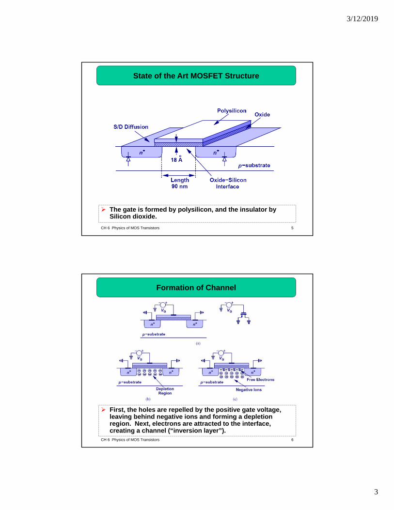
State of the Art MOSFET Structure
The gate is formed by polysilicon, and the insulator by Silicon dioxide.
CH 6 Physics of MOS Transistors 6
Formation of Channel
First, the holes are repelled by the positive gate voltage, leaving behind negative ions and forming a depletion region. Next, electrons are attracted to the interface, creating a channel (“inversion layer”).

3/12/2019
4
CH 6 Physics of MOS Transistors 7
Voltage-Dependent Resistor
The inversion channel of a MOSFET can be seen as a resistor.
Since the charge density inside the channel depends on the gate voltage, this resistance is also voltage-dependent.
CH 6 Physics of MOS Transistors 8
Voltage-Controlled Attenuator
As the gate voltage decreases, the output drops because the channel resistance increases.
This type of gain control finds application in cell phones to avoid saturation near base stations.

3/12/2019
5
CH 6 Physics of MOS Transistors 9
MOSFET Characteristics
The MOS characteristics are measured by varying VG while keeping VD constant, and varying VD while keeping VG constant.
(d) shows the voltage dependence of channel resistance.
CH 6 Physics of MOS Transistors 10
L and tox Dependence
Small gate length and oxide thickness yield low channel resistance, which will increase the drain current.

3/12/2019
6
CH 6 Physics of MOS Transistors 11
Effect of W
As the gate width increases, the current increases due to a decrease in resistance. However, gate capacitance also increases thus, limiting the speed of the circuit.
An increase in W can be seen as two devices in parallel.
CH 6 Physics of MOS Transistors 12
Channel Potential Variation
Since there’s a channel resistance between drain and source, and if drain is biased higher than the source, channel potential increases from source to drain, and the potential between gate and channel will decrease from source to drain.

3/12/2019
7
CH 6 Physics of MOS Transistors 13
Channel Pinch-Off
As the potential difference between drain and gate becomes more positive, the inversion layer beneath the interface starts to pinch off around drain.
When VD – VG = Vth, the channel at drain totally pinches off, and when VD – VG > Vth, the channel length starts to decrease.
CH 6 Physics of MOS Transistors 14
Channel Charge Density
The channel charge density is equal to the gate capacitance times the gate voltage in excess of the threshold voltage.
)( THGSox VVWCQ

3/12/2019
8
CH 6 Physics of MOS Transistors 15
Charge Density at a Point
Let x be a point along the channel from source to drain, and V(x) its potential; the expression above gives the charge density (per unit length).
THGSox VxVVWCxQ )()(
CH 6 Physics of MOS Transistors 16
Charge Density and Current
The current that flows from source to drain (electrons) is related to the charge density in the channel by the charge velocity.
vQI

3/12/2019
9
CH 6 Physics of MOS Transistors 17
Drain Current
2)(221
)()(
DSDSTHGSoxnD
nTHGSoxD
n
VVVVLW
CI
dxxdV
VxVVWCI
dxdV
v
CH 6 Physics of MOS Transistors 18
Parabolic ID-VDS Relationship
By keeping VG constant and varying VDS, we obtain a parabolic relationship.
The maximum current occurs when VDS equals to VGS- VTH.

3/12/2019
10
CH 6 Physics of MOS Transistors 19
ID-VDS for Different Values of VGS
2max, THGSD VVI
CH 6 Physics of MOS Transistors 20
Linear Resistance
At small VDS, the transistor can be viewed as a resistor, with the resistance depending on the gate voltage.
It finds application as an electronic switch.
THGSoxn
on
VVLW
CR
1
3/12/2019
11
CH 6 Physics of MOS Transistors 21
Application of Electronic Switches
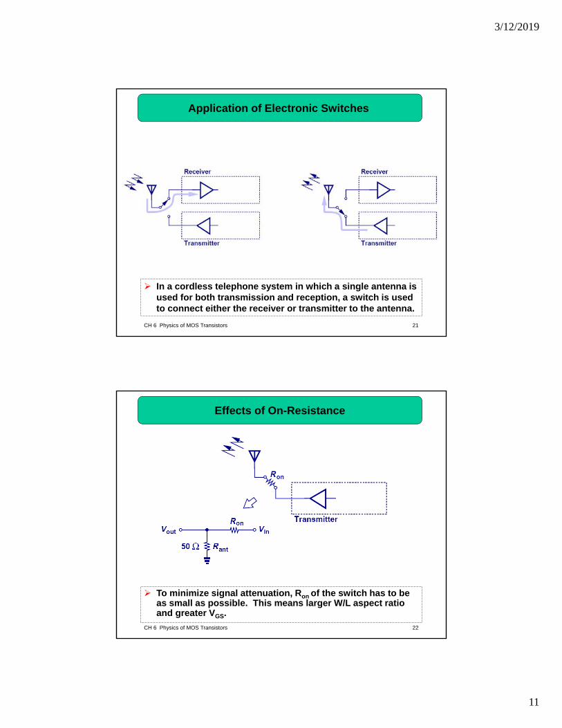
In a cordless telephone system in which a single antenna is used for both transmission and reception, a switch is used to connect either the receiver or transmitter to the antenna.
CH 6 Physics of MOS Transistors 22
Effects of On-Resistance
To minimize signal attenuation, Ron of the switch has to be as small as possible. This means larger W/L aspect ratio and greater VGS.

3/12/2019
12
CH 6 Physics of MOS Transistors 23
Different Regions of Operation
CH 6 Physics of MOS Transistors 24
How to Determine ‘Region of Operation’
When the potential difference between gate and drain is greater than VTH, the MOSFET is in triode region.
When the potential difference between gate and drain becomes equal to or less than VTH, the MOSFET enters saturation region.

3/12/2019
13
CH 6 Physics of MOS Transistors 25
Triode or Saturation?
When the region of operation is not known, a region is assumed (with an intelligent guess). Then, the final answer is checked against the assumption.
CH 6 Physics of MOS Transistors 26
Channel-Length Modulation
The original observation that the current is constant in the saturation region is not quite correct. The end point of the channel actually moves toward the source as VD increases, increasing ID. Therefore, the current in the saturation region is a weak function of the drain voltage.
DSTHGSoxnD VVVLW
CI 121 2

3/12/2019
14
CH 6 Physics of MOS Transistors 27
and L
Unlike the Early voltage in BJT, the channel- length modulation factor can be controlled by the circuit designer.
For long L, the channel-length modulation effect is less than that of short L.
CH 6 Physics of MOS Transistors 28
Transconductance
Transconductance is a measure of how strong the drain current changes when the gate voltage changes.
It has three different expressions.
THGSoxnm VVLW
Cg Doxnm ILW
Cg 2THGS
Dm VV
Ig
2
3/12/2019
15
CH 6 Physics of MOS Transistors 29
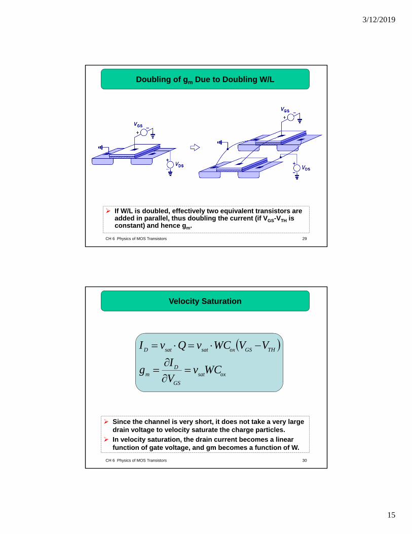
Doubling of gm Due to Doubling W/L
If W/L is doubled, effectively two equivalent transistors are added in parallel, thus doubling the current (if VGS-VTH is constant) and hence gm.
CH 6 Physics of MOS Transistors 30
Velocity Saturation
Since the channel is very short, it does not take a very large drain voltage to velocity saturate the charge particles.
In velocity saturation, the drain current becomes a linear function of gate voltage, and gm becomes a function of W.
oxsat
GS
Dm
THGSoxsatsatD
WCvV
Ig
VVWCvQvI
3/12/2019
16
CH 6 Physics of MOS Transistors 31
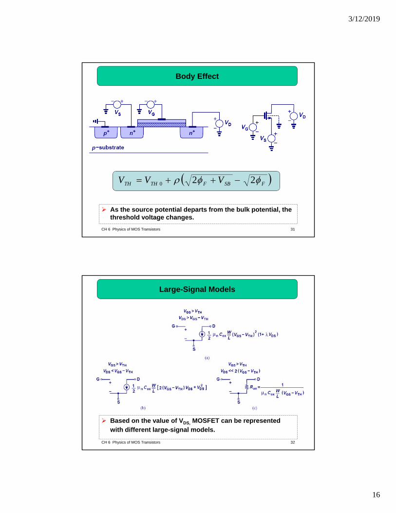
Body Effect
As the source potential departs from the bulk potential, the threshold voltage changes.
FSBFTHTH VVV 220
CH 6 Physics of MOS Transistors 32
Large-Signal Models
Based on the value of VDS, MOSFET can be represented
with different large-signal models.

3/12/2019
17
CH 6 Physics of MOS Transistors 33
Example: Behavior of ID with V1 as a Function
Since V1 is connected at the source, as it increases, the current drops.
2121
THDDoxnD VVVLW
CI
CH 6 Physics of MOS Transistors 34
Small-Signal Model
When the bias point is not perturbed significantly, small-signal model can be used to facilitate calculations.
To represent channel-length modulation, an output resistance is inserted into the model.
D
o Ir
1

3/12/2019
18
CH 6 Physics of MOS Transistors 35
PMOS Transistor
Just like the PNP transistor in bipolar technology, it is possible to create a MOS device where holes are the dominant carriers. It is called the PMOS transistor.
It behaves like an NMOS device with all the polarities reversed.
CH 6 Physics of MOS Transistors 36
PMOS Equations
2,
2
,
2,
2
,
221
121
221
)1(21
DSDSTHGSoxptriD
DSTHGSoxpsatD
DSDSTHGSoxptriD
DSTHGSoxpsatD
VVVVLW
CI
VVVLW
CI
VVVVLW
CI
VVVLW
CI

3/12/2019
19
CH 6 Physics of MOS Transistors 37
Small-Signal Model of PMOS Device
The small-signal model of PMOS device is identical to that of NMOS transistor; therefore, RX equals RY and hence (1/gm)||ro.
CH 6 Physics of MOS Transistors 38
CMOS Technology
It possible to grow an n-well inside a p-substrate to create a technology where both NMOS and PMOS can coexist.
It is known as CMOS, or “Complementary MOS”.

3/12/2019
20
CH 6 Physics of MOS Transistors 39
Comparison of Bipolar and MOS Transistors
Bipolar devices have a higher gm than MOSFETs for a given bias current due to its exponential IV characteristics.
40
Chapter 7 CMOS Amplifiers
7.1 General Considerations
7.2 Common-Source Stage
7.3 Common-Gate Stage
7.4 Source Follower
7.5 Summary and Additional Examples
3/12/2019
21
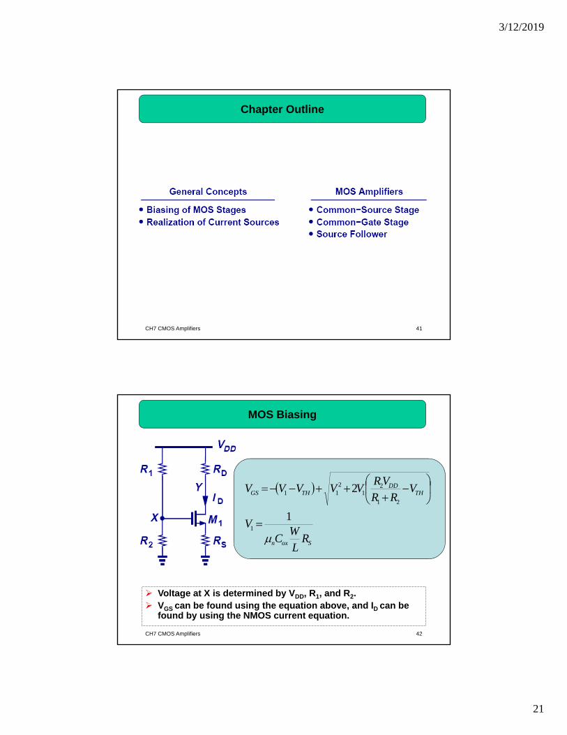
CH7 CMOS Amplifiers 41
Chapter Outline
CH7 CMOS Amplifiers 42
MOS Biasing
Voltage at X is determined by VDD, R1, and R2. VGS can be found using the equation above, and ID can be
found by using the NMOS current equation.
Soxn
THDD
THGS
RLW
CV
VRR
VRVVVVV
1
2
1
21
21
211

3/12/2019
22
CH7 CMOS Amplifiers 43
Self-Biased MOS Stage
The circuit above is analyzed by noting M1 is in saturation and no potential drop appears across RG.
DDDSGSDD VIRVRI
CH7 CMOS Amplifiers 44
Current Sources
When in saturation region, a MOSFET behaves as a current source.
NMOS draws current from a point to ground (sinks current), whereas PMOS draws current from VDD to a point (sources current).

3/12/2019
23
CH7 CMOS Amplifiers 45
Common-Source Stage
DDoxnv
Dmv
RIL
WCA
RgA
2
0
CH7 CMOS Amplifiers 46
Operation in Saturation
In order to maintain operation in saturation, Vout cannot fall below Vin by more than one threshold voltage.
The condition above ensures operation in saturation.
THGSDDDD VVVIR
3/12/2019
24
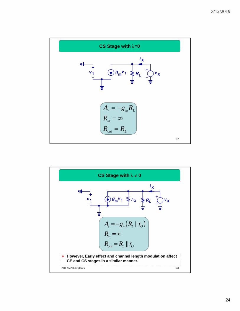
47
CS Stage with =0
Lout
in
Lmv
RR
R
RgA
CH7 CMOS Amplifiers 48
CS Stage with 0
However, Early effect and channel length modulation affect CE and CS stages in a similar manner.
OLout
in
OLmv
rRR
R
rRgA
||
||
3/12/2019
25
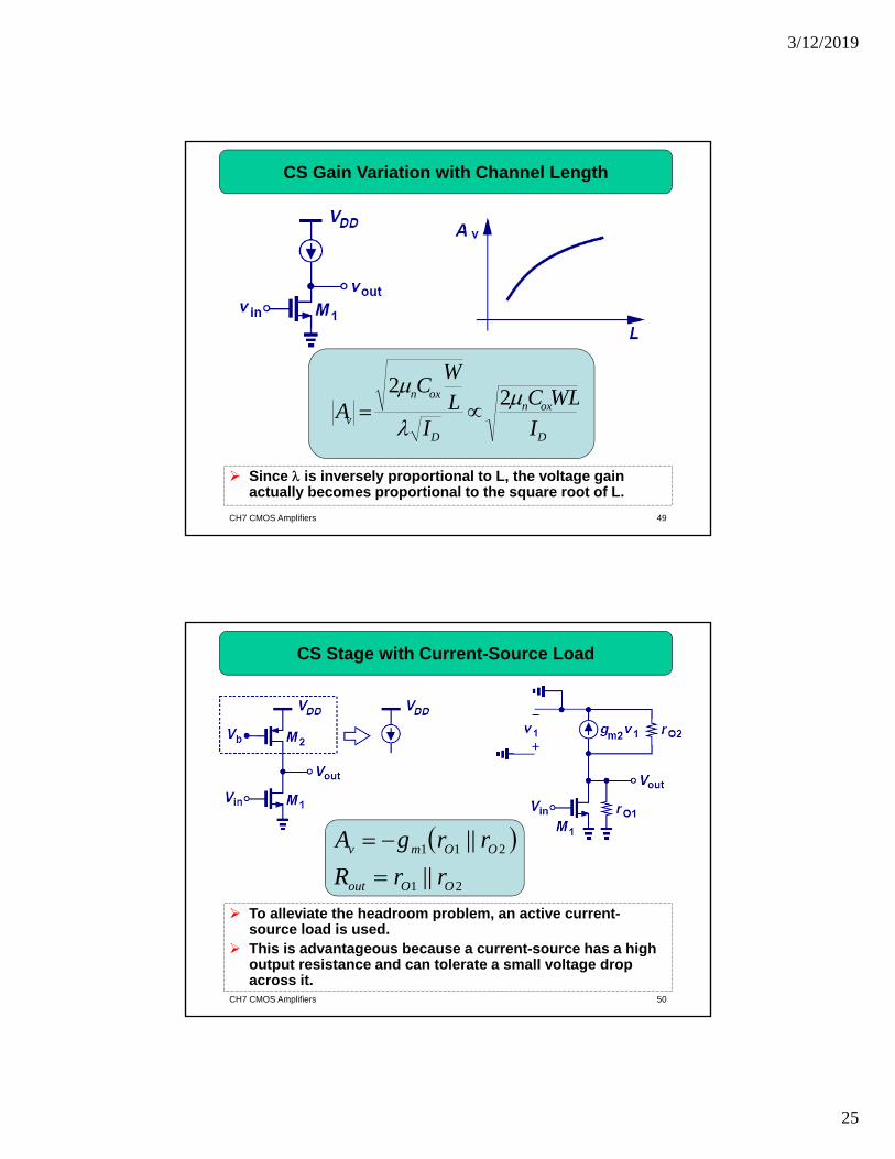
CH7 CMOS Amplifiers 49
CS Gain Variation with Channel Length
Since is inversely proportional to L, the voltage gain actually becomes proportional to the square root of L.
D
oxn
D
oxn
v I
WLC
ILW
CA
22
CH7 CMOS Amplifiers 50
CS Stage with Current-Source Load
To alleviate the headroom problem, an active current-source load is used.
This is advantageous because a current-source has a high output resistance and can tolerate a small voltage drop across it.
21
211
||
||
OOout
OOmv
rrR
rrgA

3/12/2019
26
CH7 CMOS Amplifiers 51
PMOS CS Stage with NMOS as Load
Similarly, with PMOS as input stage and NMOS as the load, the voltage gain is the same as before.
)||( 212 OOmv rrgA
CH7 CMOS Amplifiers 52
CS Stage with Diode-Connected Load
Lower gain, but less dependent on process parameters.
12
2
1
2
1
2
1
||||1
//1
OO
m
mv
m
mv
rrg
gA
LWLW
ggA

3/12/2019
27
53
CS Stage with Diode-Connected PMOS Device
Note that PMOS circuit symbol is usually drawn with the source on top of the drain.
21
1
2 ||||1
oo
m
mv rrg
gA
CH7 CMOS Amplifiers 54
CS Stage with Degeneration
Similar to bipolar counterpart, when a CS stage is degenerated, its gain, I/O impedances, and linearity change.
0
1
S
m
Dv
Rg
RA

3/12/2019
28
CH7 CMOS Amplifiers 55
Example of CS Stage with Degeneration
A diode-connected device degenerates a CS stage.
21
11
mm
Dv
gg
RA
CH7 CMOS Amplifiers 56
CS Stage with Gate Resistance
Since at low frequencies, the gate conducts no current, gate resistance does not affect the gain or I/O impedances.
0GRV

3/12/2019
29
CH7 CMOS Amplifiers 57
Output Impedance of CS Stage with Degeneration
Similar to the bipolar counterpart, degeneration boosts output impedance.
OSOmout rRrgr
CH7 CMOS Amplifiers 58
Output Impedance Example (I)
When 1/gm is parallel with rO2, we often just consider 1/gm.
22
11
111
mm
mOout gggrR
3/12/2019
30
CH7 CMOS Amplifiers 59
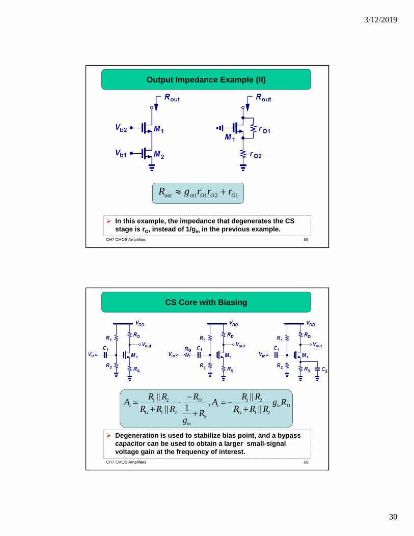
Output Impedance Example (II)
In this example, the impedance that degenerates the CS stage is rO, instead of 1/gm in the previous example.
1211 OOOmout rrrgR
CH7 CMOS Amplifiers 60
CS Core with Biasing
Degeneration is used to stabilize bias point, and a bypass capacitor can be used to obtain a larger small-signal voltage gain at the frequency of interest.
Dm
G
v
S
m
D
G
v RgRRR
RRA
Rg
RRRR
RRA
21
21
21
21
||||
,1||
||
3/12/2019
31
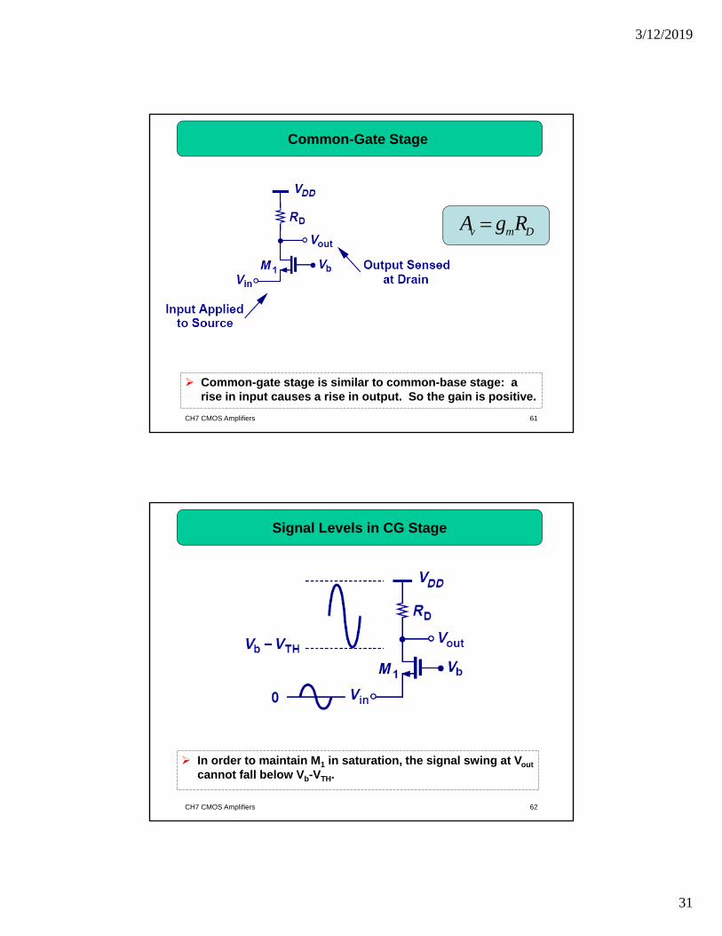
CH7 CMOS Amplifiers 61
Common-Gate Stage
Common-gate stage is similar to common-base stage: a rise in input causes a rise in output. So the gain is positive.
Dmv RgA
CH7 CMOS Amplifiers 62
Signal Levels in CG Stage
In order to maintain M1 in saturation, the signal swing at Vout
cannot fall below Vb-VTH.

3/12/2019
32
CH7 CMOS Amplifiers 63
I/O Impedances of CG Stage
The input and output impedances of CG stage are similar to those of CB stage.
Dout RR m
in gR
1 0
CH7 CMOS Amplifiers 64
CG Stage with Source Resistance
When a source resistance is present, the voltage gain is equal to that of a CS stage with degeneration, only positive.
S
m
Dv
Rg
RA
1

3/12/2019
33
CH7 CMOS Amplifiers 65
Generalized CG Behavior
When a gate resistance is present it does not affect the gain and I/O impedances since there is no potential drop across it ( at low frequencies).
The output impedance of a CG stage with source resistance is identical to that of CS stage with degeneration.
OSOmout rRrgR 1
CH7 CMOS Amplifiers 66
Example of CG Stage
Diode-connected M2 acts as a resistor to provide the bias current.
DOS
m
Omout RrRg
rgR ||||1
1
2
11
Smm
Dm
in
out
RggRg
vv
21
1
1

3/12/2019
34
CH7 CMOS Amplifiers 67
CG Stage with Biasing
R1 and R2 provide gate bias voltage, and R3 provides a path for DC bias current of M1 to flow to ground.
Dm
Sm
m
in
out RgRgR
gRvv
/1||
/1||
3
3
CH7 CMOS Amplifiers 68
Source Follower Stage
1vA

3/12/2019
35
CH7 CMOS Amplifiers 69
Source Follower Core
Similar to the emitter follower, the source follower can be analyzed as a resistor divider.
LO
m
LO
in
out
Rrg
Rrvv
||1
||
CH7 CMOS Amplifiers 70
Source Follower Example
In this example, M2 acts as a current source.
21
1
21
||1
||
OO
m
OOv
rrg
rrA

3/12/2019
36
CH7 CMOS Amplifiers 71
Output Resistance of Source Follower
The output impedance of a source follower is relatively low, whereas the input impedance is infinite ( at low frequencies); thus, a good candidate as a buffer.
L
m
LO
m
out Rg
Rrg
R ||1
||||1
CH7 CMOS Amplifiers 72
Source Follower with Biasing
RG sets the gate voltage to VDD, whereas RS sets the drain current.
The quadratic equation above can be solved for ID.
221
THSDDDoxnD VRIVLW
CI

3/12/2019
37
CH7 CMOS Amplifiers 73
Supply-Independent Biasing
If Rs is replaced by a current source, drain current IDbecomes independent of supply voltage.
CH7 CMOS Amplifiers 74
Example of a CS Stage (I)
M1 acts as the input device and M2, M3 as the load.
321
3
321
3
1
||||||1
||||||1
OOO
m
out
OOO
m
mv
rrrg
R
rrrg
gA

3/12/2019
38
CH7 CMOS Amplifiers 75
Example of a CS Stage (II)
M1 acts as the input device, M3 as the source resistance, and M2 as the load.
3
31
2
||11
O
mm
Ov
rgg
rA
CH7 CMOS Amplifiers 76
Examples of CS and CG Stages
With the input connected to different locations, the two circuits, although identical in other aspects, behave differently.
S
m
OCGv
Rg
rA
12
_ 11112_ ||)1( OOSOmmCSv rrRrggA

3/12/2019
39
CH7 CMOS Amplifiers 77
By replacing the left side with a Thevenin equivalent, and recognizing the right side is actually a CG stage, the voltage gain can be easily obtained.
Example of a Composite Stage (I)
21
11
mm
Dv
gg
RA
CH7 CMOS Amplifiers 78
Example of a Composite Stage (II)
This example shows that by probing different places in a circuit, different types of output can be obtained.
Vout1 is a result of M1 acting as a source follower whereas Vout2 is a result of M1 acting as a CS stage with degeneration.
1
2
2
43
32
1||
1
||||1
m
O
m
OO
m
in
out
gr
g
rrg
vv