Embed Size (px)
Citation preview
© WJEC CBAC Ltd 2018205
GCE A level Electronics – Chapter 6: Audio Systems
Chapter 6: Audio Systems
Learning Objectives:
At the end of this topic you will be able to:• recall the structure of a simple audio system based upon preamplifiers, a
mixer, tone controls, a power amplifier and output loudspeaker;• analyse and design a multi-stage voltage preamplifier to meet bandwidth and
gain requirements;• analyse and design a mixer circuit based on a summing amplifier;• describe and explain the operation of first order active filters (bass boost,
treble boost, bass cut, treble cut) based on an op-amp inverting amplifier and select and apply the following equation to calculate the break frequency:
fb = 1
2π RC
• recall and apply the maximum power transfer theorem;• draw circuits for and recall the properties of emitter follower and source
follower power amplifiers (VOUT ≈ VIN − 0.7 for an emitter follower and VOUT ≈ VIN − 3 for source follower);• draw circuits for and recall the properties of push-pull power amplifiers
consisting of either emitter followers or source followers and select and apply the equation:
PMAX = VS2
8RL
• analyse and draw graphs of the waveforms for first order active filters, emitter follower and source follower power amplifiers and push-pull power amplifiers;
• describe crossover distortion in push-pull amplifiers and its removal using negative feedback.
© WJEC CBAC Ltd 2018206
GCE A level Electronics – Chapter 6: Audio Systems
1. Overview - a typical audio system
Learning Objectives:
At the end of this topic you will be able to:• recall the structure of a simple audio system based upon preamplifiers, a
mixer, tone controls, a power amplifier and output loudspeaker;• analyse and design a multi-stage voltage preamplifier to meet bandwidth and
gain requirements
A mono audio system is shown in the diagram.
Typical input sources are microphones, CD players, MP3 players and musical instruments such as keyboards. These generate alternating voltage signals, which are then processed by the other sub-systems.
The preamplifiers are voltage amplifiers. These are based on non-inverting voltage amplifiers, because these offer much higher input impedance than inverting amplifiers and so draw less current from the signal source.
Mixing desks are at the heart of television, radio and recording studios. They are impressive pieces of kit, with expanses of slide controls and bar graph LED displays. They are used to combine input signals, from a number of microphones, from tape players, from keyboards and other musical instruments. They allow each to be ‘faded’ in or out. At their heart is a simple circuit based on an op-amp summing amplifier.
Tone controls allow the user to emphasise high (treble) or low (bass) notes. This may be to compensate for factors that arose during recording or that are caused by the room in which the system is used. It may be to suit the mood, or preferences of the listener.
The power amplifier has the job of producing both current and voltage signals to drive the loudspeaker. We revisit the emitter follower as one way to do this and extend the treatment to the push-pull power amplifier.
In this topic, we explore the electronics behind each of the sub-systems that make up a typical audio system like the one above.
© WJEC CBAC Ltd 2018207
GCE A level Electronics – Chapter 6: Audio Systems
Signal transfer:
In designing an audio system, it is important to consider how effectively the signal is transferred from one sub-system to the next. Through most of the audio system, we aim to pass the voltage signal between stages with as little loss as possible, but pay little heed to current.
However, in the final link, between power amplifier and loudspeaker, the requirement is different- to transfer power effectively from one sub-system to the next.
Conditions for maximum voltage transfer between sub-systems - a review:
As described in the AS E-book, Thevenin’s theorem states that the output of a sub-system can be consid-ered as a voltage source in series with an internal equivalent resistance.
Hence, for the microphone:
On the other hand, the input of a sub-system, in this case a preamplifier, looks like an input resistance connected from the input terminal to 0V.
The next diagram combines both ideas:
In the audio system, the first challenge is to design the system so that as much as possible of the voltage from each sub-system is passed on to the next sub-system. In other words, using the labels on the diagram above, we want: VIN ≈ VMIC
The arrangement above is actually a voltage divider circuit, as shown in the next diagram.
Since: VMIC = VIN + VR
we need to make VR, the voltage drop across ROUT, much smaller than VIN. To do this, we make RIN much bigger than ROUT.
So far, we have referred to the input and output resistance of sub-systems. More generally, with AC signals, we should use impedance rather than resistance.
In general, to maximise voltage transfer from one sub-system to the next, the input impedance of the second sub-system should be much larger than the output impedance of the first.
© WJEC CBAC Ltd 2018208
GCE A level Electronics – Chapter 6: Audio Systems
Multi-stage voltage preamplifier:
The AS E-book introduced a quantity called the ‘gain-bandwidth product’ of an op-amp. In designing voltage amplifiers, there is usually a trade-off between voltage gain and bandwidth (range of frequencies that is amplified).
The bigger the voltage gain, the smaller the bandwidth (and vice-versa).
For example:A 741 op-amp has a gain-bandwidth product of 1 MHz, (= 1 000 000 Hz). The full audio frequency range runs from 20 Hz to 20 kHz, (i.e. a bandwidth of 20 kHz).With this bandwidth, a 741 op-amp amplifier cannot have a voltage gain bigger than 50,(since 50 x 20 000 = 1 000 000).
However, a multi-stage preamplifier offers a way around this limitation.The next diagram shows a two-stage preamplifier made from two voltage amplifiers, each with a bandwidth of 20 kHz, cascaded together, (the output of the first amplifier provides the input to the second).
Assuming that the two op-amps have a gain-bandwidth product of 1 MHz, separately each amplifier has a voltage gain of 50. However, cascaded, the overall gain is 50 x 50 (= 2500).
The first amplifier has a bandwidth of 20 kHz, and so amplifies all frequencies in the audio range success-fully, as does the second amplifier. Overall, the system has a bandwidth of 20 kHz and a voltage gain of 2500.
In this way we can have both bandwidth and voltage gain.
An important design pointWe could get a voltage gain of 2500 by cascading an amplifier with a gain of 25 with a second one having a gain of 100, as shown below:
The first preamplifier would have a bandwidth of 40 kHz, but the second would have only 10 kHz. Although the first amplifier boosts signals with frequencies all the way up to 40 kHz, the second boosts only those with frequencies below 10 kHz, and rejects all others.
The high bandwidth of the first stage is wasted - the overall bandwidth of the cascaded amplifiers is only 10 kHz.
© WJEC CBAC Ltd 2018209
GCE A level Electronics – Chapter 6: Audio Systems
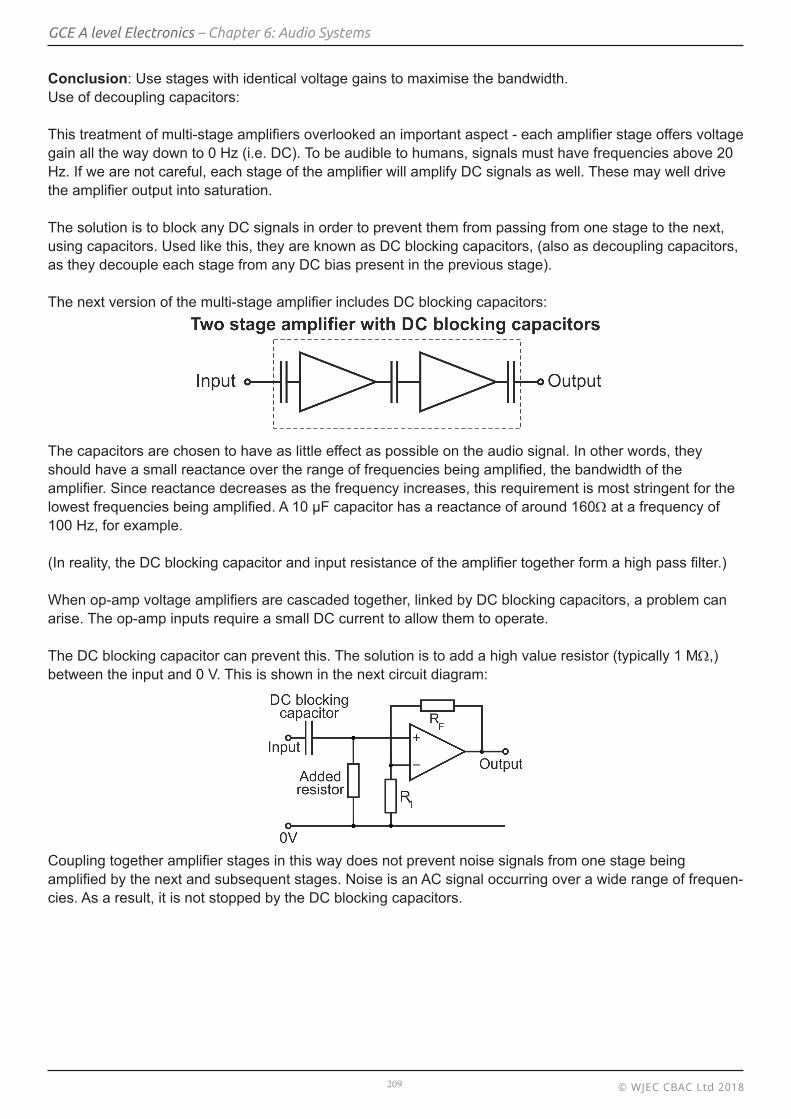
Conclusion: Use stages with identical voltage gains to maximise the bandwidth.Use of decoupling capacitors:
This treatment of multi-stage amplifiers overlooked an important aspect - each amplifier stage offers voltage gain all the way down to 0 Hz (i.e. DC). To be audible to humans, signals must have frequencies above 20 Hz. If we are not careful, each stage of the amplifier will amplify DC signals as well. These may well drive the amplifier output into saturation.
The solution is to block any DC signals in order to prevent them from passing from one stage to the next, using capacitors. Used like this, they are known as DC blocking capacitors, (also as decoupling capacitors, as they decouple each stage from any DC bias present in the previous stage).
The next version of the multi-stage amplifier includes DC blocking capacitors:
The capacitors are chosen to have as little effect as possible on the audio signal. In other words, they should have a small reactance over the range of frequencies being amplified, the bandwidth of the amplifier. Since reactance decreases as the frequency increases, this requirement is most stringent for the lowest frequencies being amplified. A 10 µF capacitor has a reactance of around 160Ω at a frequency of 100 Hz, for example.
(In reality, the DC blocking capacitor and input resistance of the amplifier together form a high pass filter.)
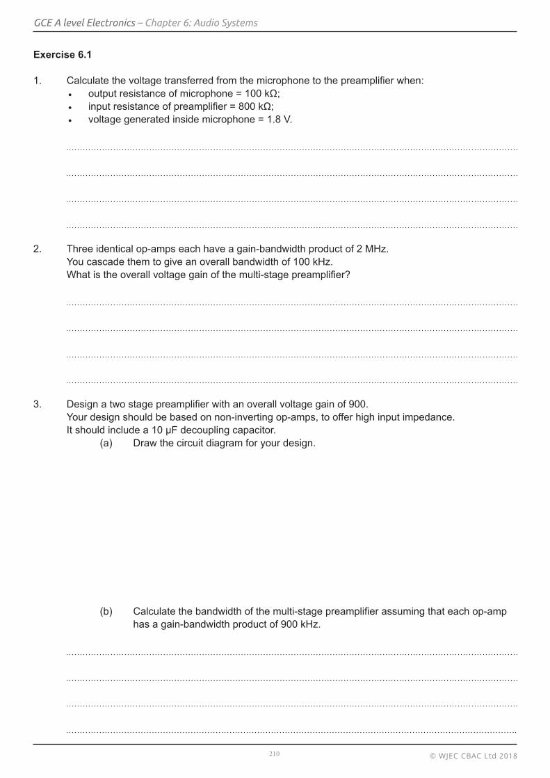
When op-amp voltage amplifiers are cascaded together, linked by DC blocking capacitors, a problem can arise. The op-amp inputs require a small DC current to allow them to operate.
The DC blocking capacitor can prevent this. The solution is to add a high value resistor (typically 1 MΩ,) between the input and 0 V. This is shown in the next circuit diagram:
Coupling together amplifier stages in this way does not prevent noise signals from one stage being amplified by the next and subsequent stages. Noise is an AC signal occurring over a wide range of frequen-cies. As a result, it is not stopped by the DC blocking capacitors.
© WJEC CBAC Ltd 2018210
GCE A level Electronics – Chapter 6: Audio Systems
Exercise 6.1
1. Calculate the voltage transferred from the microphone to the preamplifier when:• output resistance of microphone = 100 kΩ;• input resistance of preamplifier = 800 kΩ;• voltage generated inside microphone = 1.8 V.
2. Three identical op-amps each have a gain-bandwidth product of 2 MHz. You cascade them to give an overall bandwidth of 100 kHz. What is the overall voltage gain of the multi-stage preamplifier?
3. Design a two stage preamplifier with an overall voltage gain of 900. Your design should be based on non-inverting op-amps, to offer high input impedance. It should include a 10 µF decoupling capacitor. (a) Draw the circuit diagram for your design.
(b) Calculate the bandwidth of the multi-stage preamplifier assuming that each op-amp has a gain-bandwidth product of 900 kHz.
© WJEC CBAC Ltd 2018211
GCE A level Electronics – Chapter 6: Audio Systems
2. The audio mixer
Learning Objectives:
At the end of this topic you will be able to:• analyse and design a mixer circuit based on a summing amplifier;
The design for the audio mixer is a development of the summing amplifier.
Summing amplifier - a review:
In the AS E-book, we examined the summing amplifier
The circuit diagram for the summing amplifier is shownopposite:
The output voltage, VOUT, is given by:
VOUT =−RF V1 +
V2 + ... R1 R2
Example:
In the above circuit, calculate the value of VOUT when:
V1 = +0.7 V; V2 = -0.8 V; V3 = + 1.2 V and R1 = 10 kΩ; R 2 = 5 kΩ; R 3 = 10 kΩ; R F = 20 kΩ. VOUT =−20kΩ + 0.7 V +
− 0.8 V + + 1.2 V
10 kΩ
5 kΩ
10 kΩ
Since all the resistor values are in kΩ, we can rewrite the equation as: VOUT = −20 + 0.7 +
− 0.8 + + 1.2
10
5
10
= −20 (0.07 − 0.016 + 0.12) = −20 (0.03) = − 0.6 V
The mixer:In a basic mixer, the input resistors have variable resistors added in series with them.The following diagram shows this:
The behaviour is exactly the same as for the summing amplifier, except that now each input resistance value used in the output voltage formula is the sum of the fixed resistor and the variable resistor. As the variable resistor is adjusted to a bigger resistance, the voltage gain on that input is reduced – that input is ‘faded out’.
© WJEC CBAC Ltd 2018212
GCE A level Electronics – Chapter 6: Audio Systems
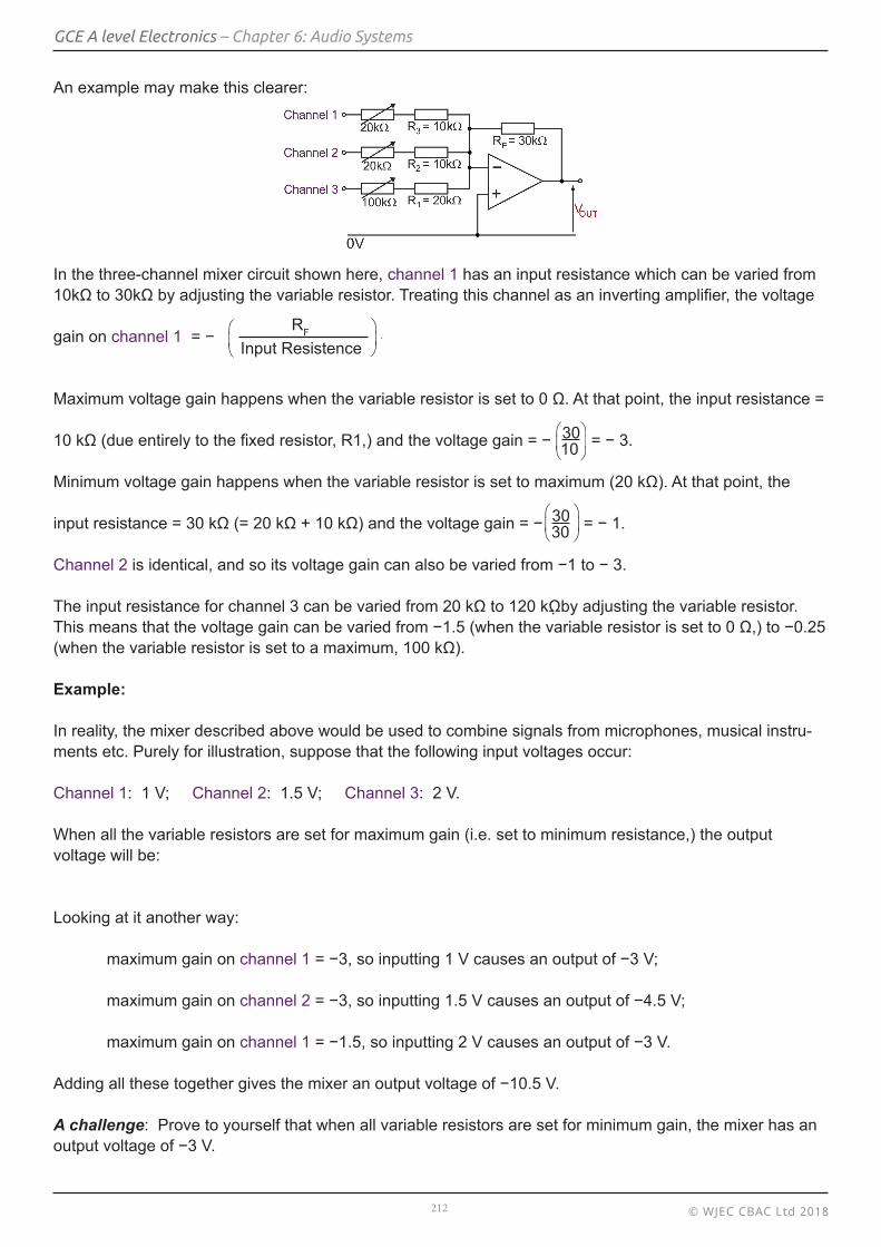
An example may make this clearer:
In the three-channel mixer circuit shown here, channel 1 has an input resistance which can be varied from 10kΩ to 30kΩ by adjusting the variable resistor. Treating this channel as an inverting amplifier, the voltage
gain on channel 1 = − RF .
Input Resistence
Maximum voltage gain happens when the variable resistor is set to 0 Ω. At that point, the input resistance =
10 kΩ (due entirely to the fixed resistor, R1,) and the voltage gain = − 30
= − 3.
10
Minimum voltage gain happens when the variable resistor is set to maximum (20 kΩ). At that point, the
input resistance = 30 kΩ (= 20 kΩ + 10 kΩ) and the voltage gain = − 30 = − 1.
30
Channel 2 is identical, and so its voltage gain can also be varied from −1 to − 3.
The input resistance for channel 3 can be varied from 20 kΩ to 120 kΩby adjusting the variable resistor. This means that the voltage gain can be varied from −1.5 (when the variable resistor is set to 0 Ω,) to −0.25 (when the variable resistor is set to a maximum, 100 kΩ).
Example:
In reality, the mixer described above would be used to combine signals from microphones, musical instru-ments etc. Purely for illustration, suppose that the following input voltages occur:
Channel 1: 1 V; Channel 2: 1.5 V; Channel 3: 2 V.
When all the variable resistors are set for maximum gain (i.e. set to minimum resistance,) the output voltage will be:
Looking at it another way:
maximum gain on channel 1 = −3, so inputting 1 V causes an output of −3 V;
maximum gain on channel 2 = −3, so inputting 1.5 V causes an output of −4.5 V;
maximum gain on channel 1 = −1.5, so inputting 2 V causes an output of −3 V.
Adding all these together gives the mixer an output voltage of −10.5 V.
A challenge: Prove to yourself that when all variable resistors are set for minimum gain, the mixer has an output voltage of −3 V.
© WJEC CBAC Ltd 2018213
GCE A level Electronics – Chapter 6: Audio Systems
Another design point:
A mixer sums input voltages. As a result, it is easy to drive the output into saturation. When designing a mixer, it is important to limit its voltage gain by keeping the value of the feedback resistor down.
Make sure that the output does not saturate when the input voltages have their maximum values.
If more voltage gain is needed, that can be provided by other components of the audio system.
A better mixer circuit:
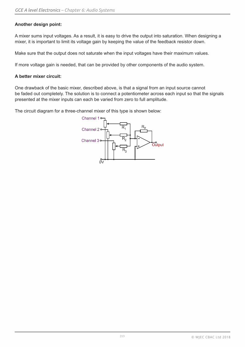
One drawback of the basic mixer, described above, is that a signal from an input source cannotbe faded out completely. The solution is to connect a potentiometer across each input so that the signals presented at the mixer inputs can each be varied from zero to full amplitude.
The circuit diagram for a three-channel mixer of this type is shown below:
© WJEC CBAC Ltd 2018214
GCE A level Electronics – Chapter 6: Audio Systems
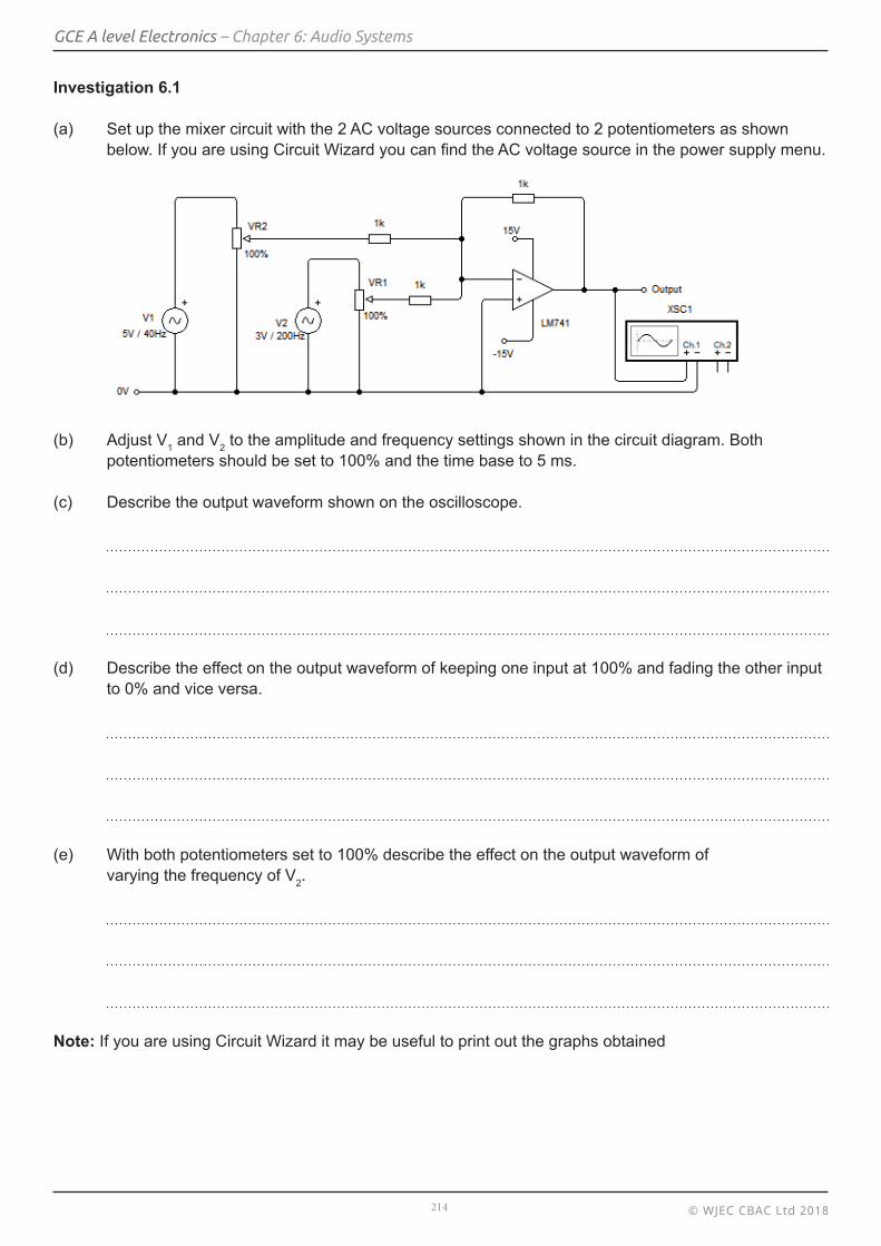
Investigation 6.1
(a) Set up the mixer circuit with the 2 AC voltage sources connected to 2 potentiometers as shown below. If you are using Circuit Wizard you can find the AC voltage source in the power supply menu.
(b) Adjust V1 and V2 to the amplitude and frequency settings shown in the circuit diagram. Both potentiometers should be set to 100% and the time base to 5 ms.
(c) Describe the output waveform shown on the oscilloscope.
(d) Describe the effect on the output waveform of keeping one input at 100% and fading the other input to 0% and vice versa.
(e) With both potentiometers set to 100% describe the effect on the output waveform of varying the frequency of V2.
Note: If you are using Circuit Wizard it may be useful to print out the graphs obtained
© WJEC CBAC Ltd 2018215
GCE A level Electronics – Chapter 6: Audio Systems
Exercise 6.2
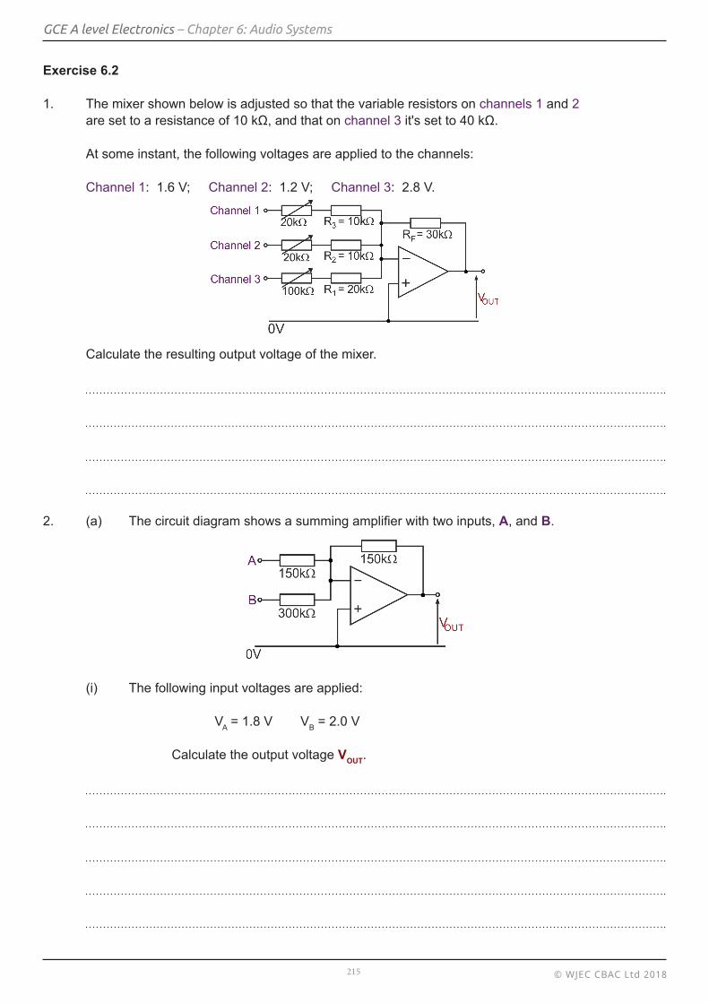
1. The mixer shown below is adjusted so that the variable resistors on channels 1 and 2 are set to a resistance of 10 kΩ, and that on channel 3 it's set to 40 kΩ.
At some instant, the following voltages are applied to the channels:
Channel 1: 1.6 V; Channel 2: 1.2 V; Channel 3: 2.8 V.
Calculate the resulting output voltage of the mixer.
2. (a) The circuit diagram shows a summing amplifier with two inputs, A, and B.
(i) The following input voltages are applied:
VA = 1.8 V VB = 2.0 V
Calculate the output voltage VOUT.
© WJEC CBAC Ltd 2018216
GCE A level Electronics – Chapter 6: Audio Systems
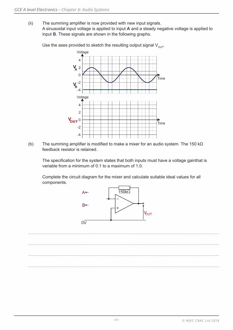
(ii) The summing amplifier is now provided with new input signals. A sinusoidal input voltage is applied to input A and a steady negative voltage is applied to input B. These signals are shown in the following graphs. Use the axes provided to sketch the resulting output signal VOUT.
(b) The summing amplifier is modified to make a mixer for an audio system. The 150 kΩ feedback resistor is retained. The specification for the system states that both inputs must have a voltage gainthat is variable from a minimum of 0.1 to a maximum of 1.0.
Complete the circuit diagram for the mixer and calculate suitable ideal values for all components.
© WJEC CBAC Ltd 2018217
GCE A level Electronics – Chapter 6: Audio Systems
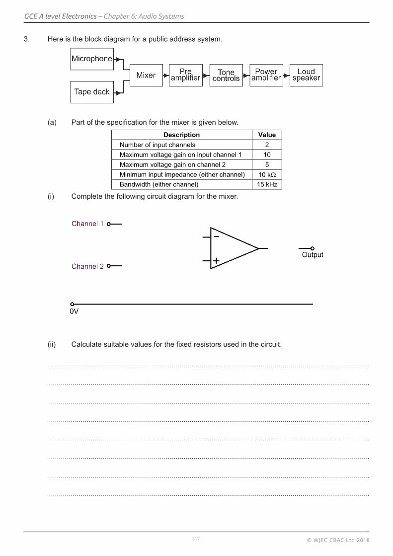
3. Here is the block diagram for a public address system.
(a) Part of the specification for the mixer is given below.
(i) Complete the following circuit diagram for the mixer.
(ii) Calculate suitable values for the fixed resistors used in the circuit.
Description Value Number of input channels 2 Maximum voltage gain on input channel 1 10 Maximum voltage gain on channel 2 5 Minimum input impedance (either channel) 10 kΩ Bandwidth (either channel) 15 kHz
© WJEC CBAC Ltd 2018218
GCE A level Electronics – Chapter 6: Audio Systems
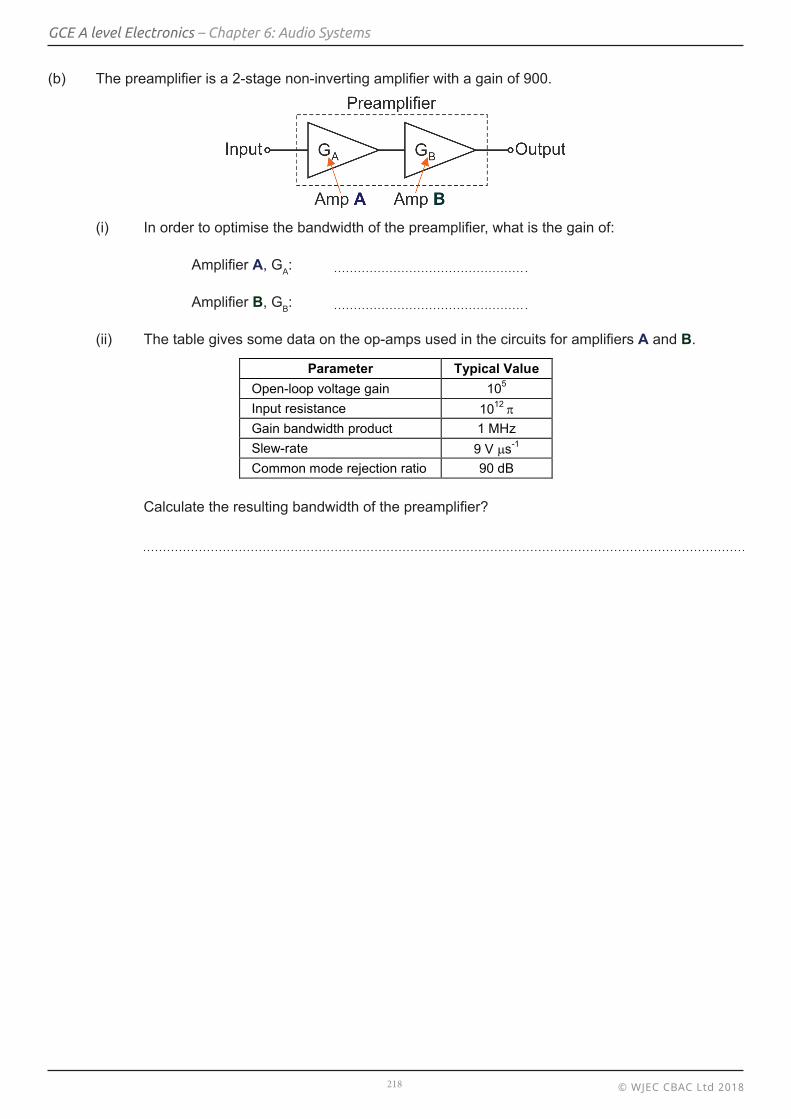
(b) The preamplifier is a 2-stage non-inverting amplifier with a gain of 900.
(i) In order to optimise the bandwidth of the preamplifier, what is the gain of:
Amplifier A, GA:
Amplifier B, GB:
(ii) The table gives some data on the op-amps used in the circuits for amplifiers A and B.
Calculate the resulting bandwidth of the preamplifier?
Parameter Typical Value Open-loop voltage gain 105 Input resistance 1012 π Gain bandwidth product 1 MHz Slew-rate 9 V µs-1 Common mode rejection ratio 90 dB
© WJEC CBAC Ltd 2018219
GCE A level Electronics – Chapter 6: Audio Systems
3. Tone control
Learning Objectives:
At the end of this topic you will be able to:• describe and explain the operation of first order active filters (bass boost,
treble boost, bass cut, treble cut) based upon an op-amp inverting amplifier and select and apply the equation to calculate the break frequency
fb = 1
2π RC
• analyse and draw graphs of the waveforms for first order active filters
The notes for Chapter 4 introduced the topic of filters, specifically low pass, high pass andband pass passive filters. These have significant limitations:
• They can only ‘cut’ - they cannot ‘boost’. In other words, they have a maximum gain of unity. For example, a low pass passive filter will reduce the amplitude of high frequency signals but cannot increase the amplitude of low frequency signals.
• Their behaviour is modified substantially when connected to a load, unless that load has a very high impedance. In situations where they have to deliver a significant current to a load, passive filters must be buffered by a suitable interface, such as an amplifier.
The active filter overcomes both of these limitations. It can have a voltage gain larger than unity for signals of a particular frequency. It includes an amplifier which can deliver current to a load without affecting the frequency response of the system.
The circuits of active filters can be complex. In this chapter, we study four basic types of filter, based on inverting voltage amplifiers using op amps. Better designs for active filters exist.
The behaviour of active filters is best studied using log-log graph paper. The approach is the same as that used previously.
We are going to rely on the ‘two-straight-lines’ approximation that was introduced earlier:
• One line is horizontal and shows the gain set by the feedback and input resistors, as in the inverting amplifier itself.
In other words, for this section of the frequency response, Voltage gain = −
RF
RIN
• The other line has a slope of 45°. The exact nature depends on the type of filter. In this part of the frequency spectrum, the resistor-capacitor (RC) network controls the behaviour.
© WJEC CBAC Ltd 2018220
GCE A level Electronics – Chapter 6: Audio Systems
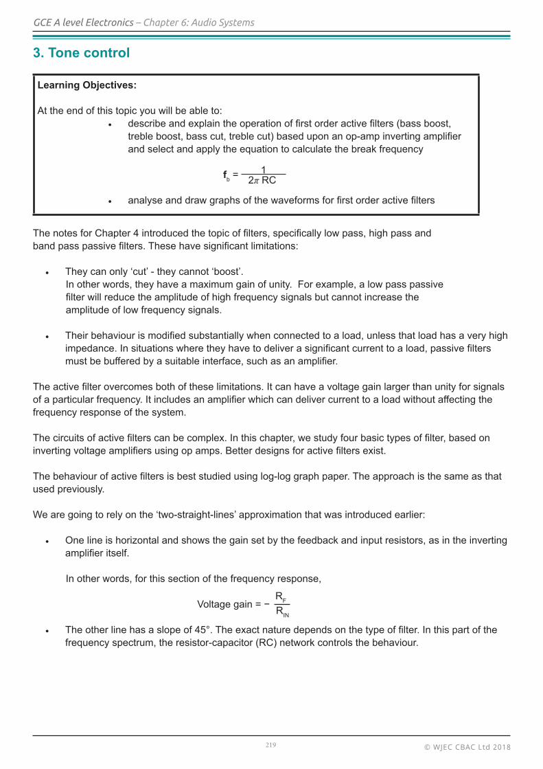
Using log-log graph paper, the four types of filter have the following characteristics:
The break frequency fb marks the boundary between the two types of behaviour.
It is defined as the frequency at which the reactance of the capacitor is equal to the resistance of the resistor that is in the RC network.
In other words, at the break frequency, fb:
R = XC
or R = 1
2π fbC
so that fb = 1
2π RC
The formula and definition are identical for all types of active filter. The only issue when applying the formula is to choose the right resistor, as there are two of them.
Use the resistor that is in the RC network, i.e. the one that is connected to the capacitor.
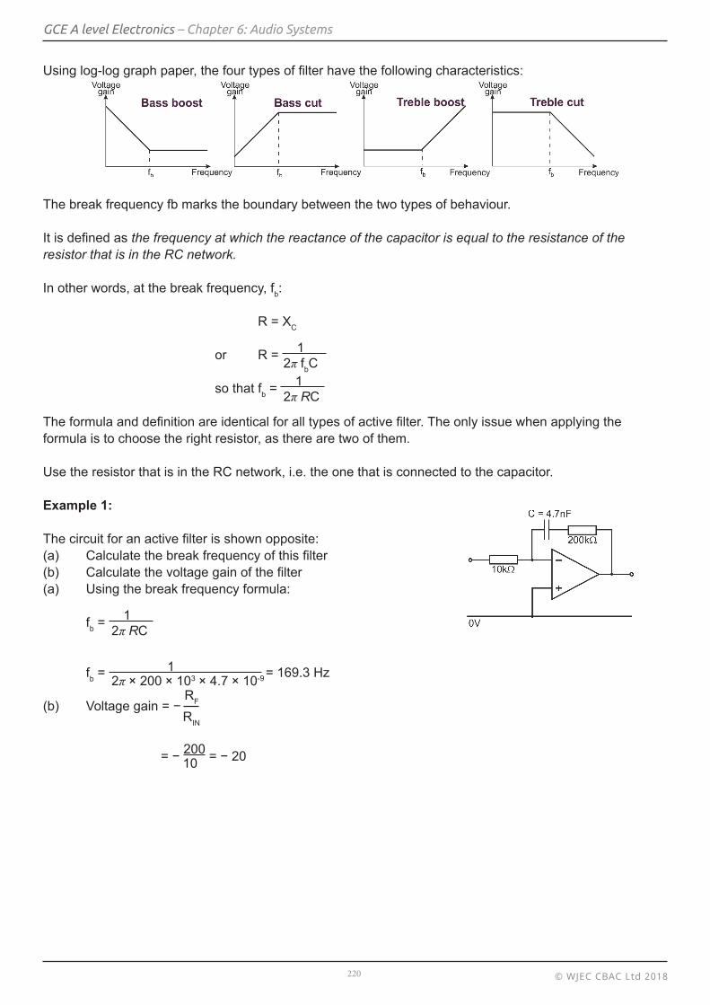
Example 1:
The circuit for an active filter is shown opposite:(a) Calculate the break frequency of this filter(b) Calculate the voltage gain of the filter(a) Using the break frequency formula:
fb = 1
2π RC
fb = 1 = 169.3 Hz 2π × 200 × 103 × 4.7 × 10-9
(b) Voltage gain = − RF
RIN
= − 200 = − 20
10
© WJEC CBAC Ltd 2018221
GCE A level Electronics – Chapter 6: Audio Systems
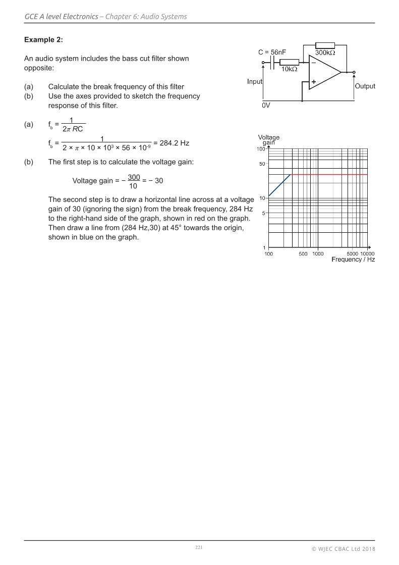
Example 2:
An audio system includes the bass cut filter shown opposite:
(a) Calculate the break frequency of this filter(b) Use the axes provided to sketch the frequency response of this filter.
(a) fb = 1
2π RC
fb = 1 = 284.2 Hz 2 × π × 10 × 103 × 56 × 10-9
(b) The first step is to calculate the voltage gain:
Voltage gain = − 300 = − 30 10
The second step is to draw a horizontal line across at a voltage gain of 30 (ignoring the sign) from the break frequency, 284 Hz to the right-hand side of the graph, shown in red on the graph. Then draw a line from (284 Hz,30) at 45° towards the origin, shown in blue on the graph.
© WJEC CBAC Ltd 2018222
GCE A level Electronics – Chapter 6: Audio Systems
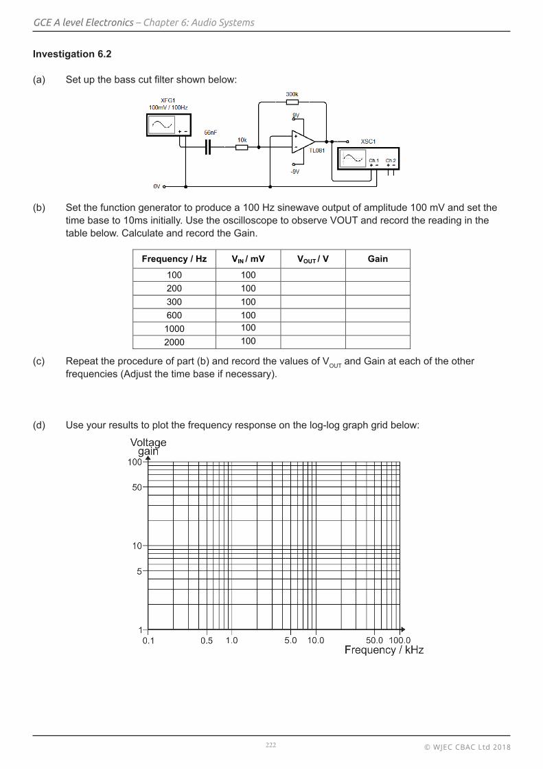
Investigation 6.2
(a) Set up the bass cut filter shown below:
(b) Set the function generator to produce a 100 Hz sinewave output of amplitude 100 mV and set the time base to 10ms initially. Use the oscilloscope to observe VOUT and record the reading in the table below. Calculate and record the Gain.
(c) Repeat the procedure of part (b) and record the values of VOUT and Gain at each of the other frequencies (Adjust the time base if necessary).
(d) Use your results to plot the frequency response on the log-log graph grid below:
Frequency / Hz VIN / mV VOUT / V Gain
100 100
200 100 300 100 600 100 1000 100 2000 100
© WJEC CBAC Ltd 2018223
GCE A level Electronics – Chapter 6: Audio Systems
(e) Use the graph to determine the cut of frequency of the filter and compare the frequency and the shape of the graph with the solution provided in example 2 above.
© WJEC CBAC Ltd 2018224
GCE A level Electronics – Chapter 6: Audio Systems
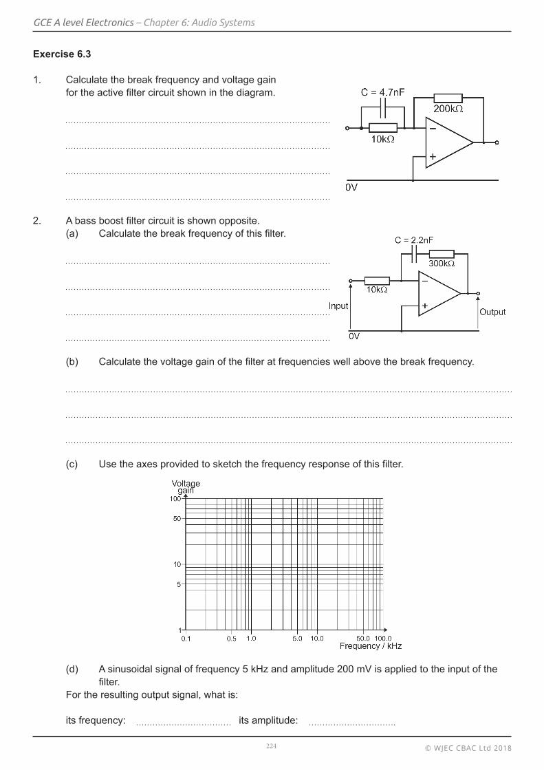
Exercise 6.3
1. Calculate the break frequency and voltage gain for the active filter circuit shown in the diagram.
2. A bass boost filter circuit is shown opposite. (a) Calculate the break frequency of this filter.
(b) Calculate the voltage gain of the filter at frequencies well above the break frequency.
(c) Use the axes provided to sketch the frequency response of this filter.
(d) A sinusoidal signal of frequency 5 kHz and amplitude 200 mV is applied to the input of the filter. For the resulting output signal, what is:
its frequency: its amplitude:
© WJEC CBAC Ltd 2018225
GCE A level Electronics – Chapter 6: Audio Systems
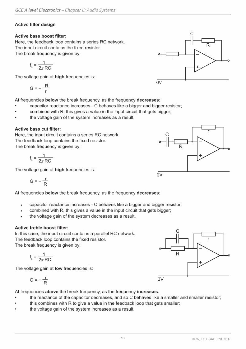
Active filter design
Active bass boost filter:Here, the feedback loop contains a series RC network. The input circuit contains the fixed resistor.The break frequency is given by:
fb = 1
2π RC
The voltage gain at high frequencies is:
G = − R
r
At frequencies below the break frequency, as the frequency decreases:• capacitor reactance increases - C behaves like a bigger and bigger resistor;• combined with R, this gives a value in the input circuit that gets bigger;• the voltage gain of the system increases as a result.
Active bass cut filter:Here, the input circuit contains a series RC network.The feedback loop contains the fixed resistor.The break frequency is given by:
fb = 1
2π RC
The voltage gain at high frequencies is:
G = − r
R
At frequencies below the break frequency, as the frequency decreases:
• capacitor reactance increases - C behaves like a bigger and bigger resistor;• combined with R, this gives a value in the input circuit that gets bigger;• the voltage gain of the system decreases as a result.
Active treble boost filter:In this case, the input circuit contains a parallel RC network.The feedback loop contains the fixed resistor.The break frequency is given by:
fb = 1
2π RC
The voltage gain at low frequencies is:
G = − r
R
At frequencies above the break frequency, as the frequency increases:• the reactance of the capacitor decreases, and so C behaves like a smaller and smaller resistor;• this combines with R to give a value in the feedback loop that gets smaller;• the voltage gain of the system increases as a result.
© WJEC CBAC Ltd 2018226
GCE A level Electronics – Chapter 6: Audio Systems
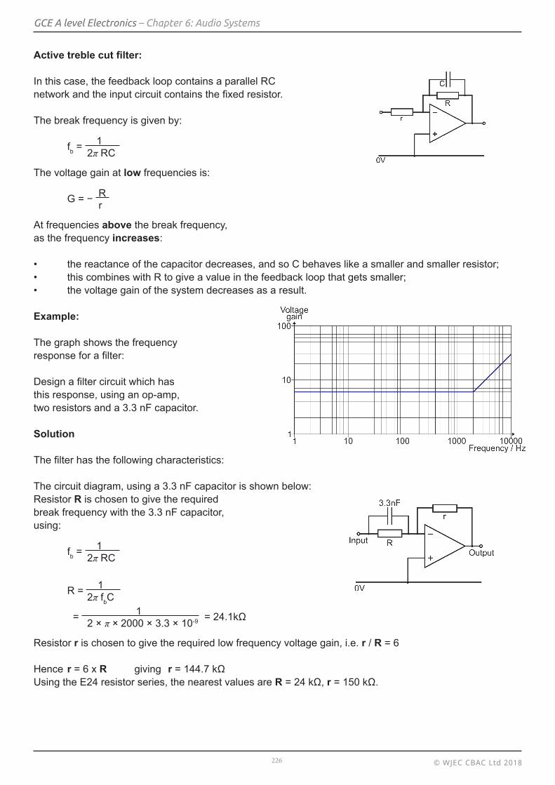
Active treble cut filter:
In this case, the feedback loop contains a parallel RCnetwork and the input circuit contains the fixed resistor.
The break frequency is given by:
fb = 1
2π RC
The voltage gain at low frequencies is: G = − R
r
At frequencies above the break frequency,as the frequency increases:
• the reactance of the capacitor decreases, and so C behaves like a smaller and smaller resistor;• this combines with R to give a value in the feedback loop that gets smaller;• the voltage gain of the system decreases as a result.
Example:
The graph shows the frequencyresponse for a filter:
Design a filter circuit which hasthis response, using an op-amp,two resistors and a 3.3 nF capacitor.
Solution
The filter has the following characteristics:
The circuit diagram, using a 3.3 nF capacitor is shown below: Resistor R is chosen to give the requiredbreak frequency with the 3.3 nF capacitor,using:
fb = 1
2π RC
R = 1
2π fbC
= 1 = 24.1kΩ 2 × π × 2000 × 3.3 × 10-9
Resistor r is chosen to give the required low frequency voltage gain, i.e. r / R = 6
Hence r = 6 x R giving r = 144.7 kΩUsing the E24 resistor series, the nearest values are R = 24 kΩ, r = 150 kΩ.
© WJEC CBAC Ltd 2018227
GCE A level Electronics – Chapter 6: Audio Systems
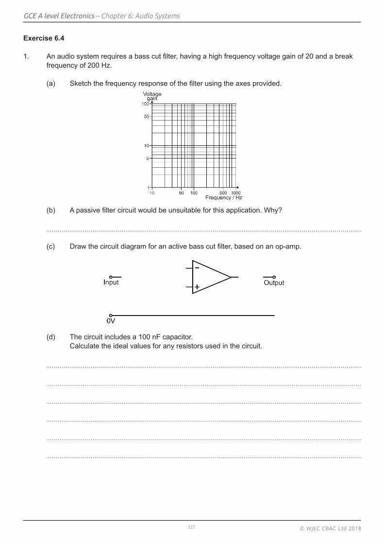
Exercise 6.4 1. An audio system requires a bass cut filter, having a high frequency voltage gain of 20 and a break frequency of 200 Hz.
(a) Sketch the frequency response of the filter using the axes provided.
(b) A passive filter circuit would be unsuitable for this application. Why?
(c) Draw the circuit diagram for an active bass cut filter, based on an op-amp.
(d) The circuit includes a 100 nF capacitor. Calculate the ideal values for any resistors used in the circuit.
© WJEC CBAC Ltd 2018228
GCE A level Electronics – Chapter 6: Audio Systems
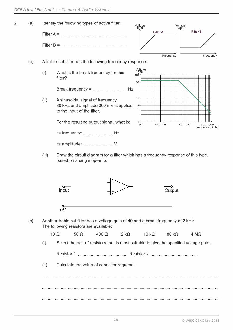
2. (a) Identify the following types of active filter:
Filter A =
Filter B =
(b) A treble-cut filter has the following frequency response:
(i) What is the break frequency for this filter?
Break frequency = Hz
(ii) A sinusoidal signal of frequency 30 kHz and amplitude 300 mV is applied to the input of the filter.
For the resulting output signal, what is:
its frequency: Hz
its amplitude: V
(iii) Draw the circuit diagram for a filter which has a frequency response of this type, based on a single op-amp.
(c) Another treble cut filter has a voltage gain of 40 and a break frequency of 2 kHz. The following resistors are available:
10 Ω 50 Ω 400 Ω 2 kΩ 10 kΩ 80 kΩ 4 MΩ
(i) Select the pair of resistors that is most suitable to give the specified voltage gain.
Resistor 1 Resistor 2
(ii) Calculate the value of capacitor required.
© WJEC CBAC Ltd 2018229
GCE A level Electronics – Chapter 6: Audio Systems
4. The power amplifier
Learning Objectives:At the end of this topic you will be able to:
• recall and apply the maximum power transfer theorem;• draw circuits for and recall the properties of emitter follower and source
follower power amplifiers (VOUT ≈ VIN − 0.7 for an emitter follower and VOUT ≈ VIN − 3 for the source follower;
• draw circuits for and recall the properties of push-pull power amplifiers based on either emitter or source followers and select and apply the equation
PMAX = VS
2
8 RL
• analyse and draw graphs of the waveforms for emitter and source follower power amplifiers and push-pull power amplifiers;
• describe crossover distortion in push-pull amplifiers and its removal using negative feedback.
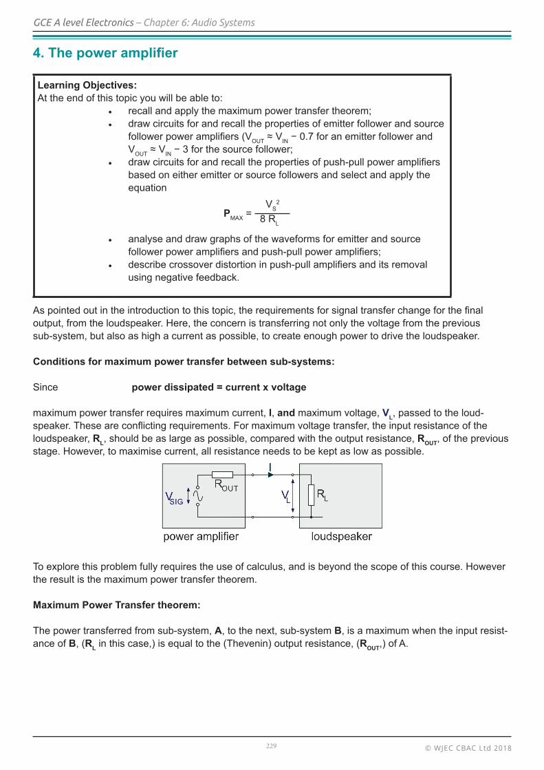
As pointed out in the introduction to this topic, the requirements for signal transfer change for the final output, from the loudspeaker. Here, the concern is transferring not only the voltage from the previous sub-system, but also as high a current as possible, to create enough power to drive the loudspeaker.
Conditions for maximum power transfer between sub-systems:
Since power dissipated = current x voltage
maximum power transfer requires maximum current, I, and maximum voltage, VL, passed to the loud-speaker. These are conflicting requirements. For maximum voltage transfer, the input resistance of the loudspeaker, RL, should be as large as possible, compared with the output resistance, ROUT, of the previous stage. However, to maximise current, all resistance needs to be kept as low as possible.
To explore this problem fully requires the use of calculus, and is beyond the scope of this course. However the result is the maximum power transfer theorem.
Maximum Power Transfer theorem:
The power transferred from sub-system, A, to the next, sub-system B, is a maximum when the input resist-ance of B, (RL in this case,) is equal to the (Thevenin) output resistance, (ROUT,) of A.
© WJEC CBAC Ltd 2018230
GCE A level Electronics – Chapter 6: Audio Systems
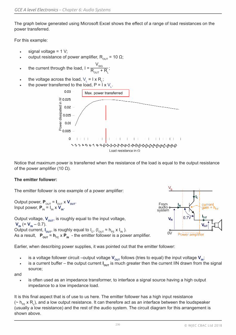
The graph below generated using Microsoft Excel shows the effect of a range of load resistances on the power transferred.
For this example:
• signal voltage = 1 V;• output resistance of power amplifier, ROUT = 10 Ω;
• the current through the load, I = VSIG ;
ROUT + RL
• the voltage across the load, VL = I x RL;• the power transferred to the load, P = I x VL.
Notice that maximum power is transferred when the resistance of the load is equal to the output resistance of the power amplifier (10 Ω).
The emitter follower:
The emitter follower is one example of a power amplifier:
Output power, POUT = IOUT x VOUT.Input power, PIN = IIN x VIN.
Output voltage, VOUT, is roughly equal to the input voltage, VIN (= VIN – 0.7). Output current, IOUT, is roughly equal to IC, (IOUT ≈ hFE x IIN ).As a result, POUT ≈ hFE x PIN - the emitter follower is a power amplifier.
Earlier, when describing power supplies, it was pointed out that the emitter follower:
• is a voltage follower circuit –output voltage VOUT follows (tries to equal) the input voltage VIN;• is a current buffer – the output current IOUT is much greater then the current IIN drawn from the signal
source;and
• is often used as an impedance transformer, to interface a signal source having a high output impedance to a low impedance load.
It is this final aspect that is of use to us here. The emitter follower has a high input resistance (~ hFE x RL), and a low output resistance. It can therefore act as an interface between the loudspeaker (usually a low resistance) and the rest of the audio system. The circuit diagram for this arrangement is shown above.
Max. power transferred MMMMax. power tttransfffferredddd
© WJEC CBAC Ltd 2018231
GCE A level Electronics – Chapter 6: Audio Systems
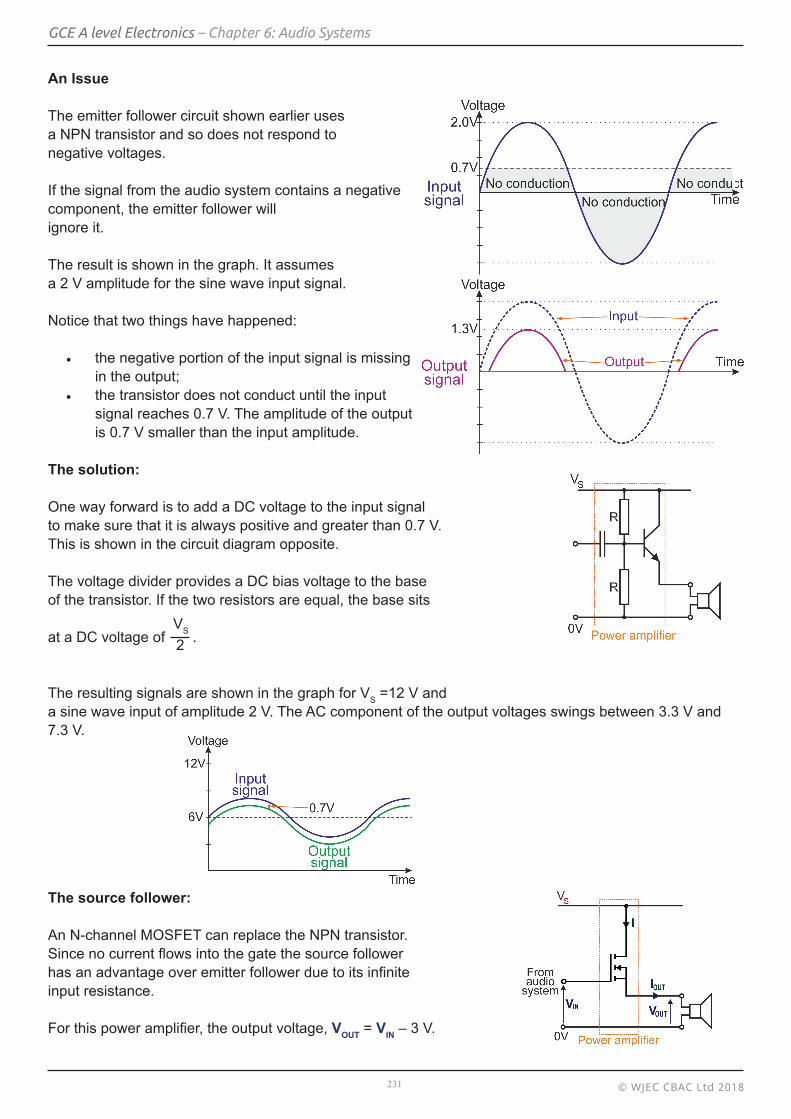
An Issue
The emitter follower circuit shown earlier usesa NPN transistor and so does not respond tonegative voltages.
If the signal from the audio system contains a negative component, the emitter follower willignore it.
The result is shown in the graph. It assumesa 2 V amplitude for the sine wave input signal.
Notice that two things have happened:
• the negative portion of the input signal is missing in the output;
• the transistor does not conduct until the input signal reaches 0.7 V. The amplitude of the output is 0.7 V smaller than the input amplitude.
The solution:
One way forward is to add a DC voltage to the input signalto make sure that it is always positive and greater than 0.7 V.This is shown in the circuit diagram opposite.
The voltage divider provides a DC bias voltage to the baseof the transistor. If the two resistors are equal, the base sits
at a DC voltage of VS .
2
The resulting signals are shown in the graph for VS =12 V anda sine wave input of amplitude 2 V. The AC component of the output voltages swings between 3.3 V and 7.3 V.
The source follower:
An N-channel MOSFET can replace the NPN transistor.Since no current flows into the gate the source followerhas an advantage over emitter follower due to its infiniteinput resistance.
For this power amplifier, the output voltage, VOUT = VIN – 3 V.
© WJEC CBAC Ltd 2018232
GCE A level Electronics – Chapter 6: Audio Systems
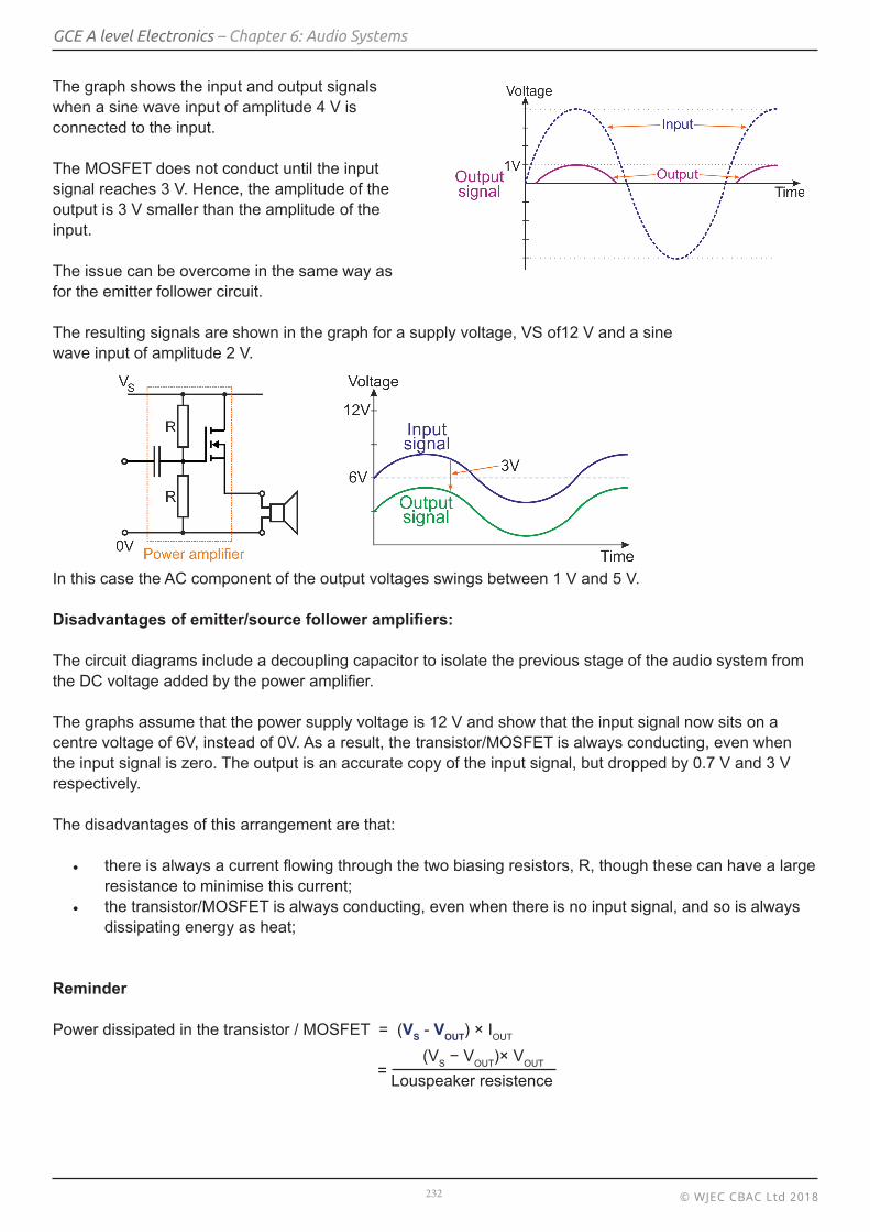
The graph shows the input and output signalswhen a sine wave input of amplitude 4 V isconnected to the input.
The MOSFET does not conduct until the inputsignal reaches 3 V. Hence, the amplitude of theoutput is 3 V smaller than the amplitude of the input.
The issue can be overcome in the same way asfor the emitter follower circuit.
The resulting signals are shown in the graph for a supply voltage, VS of12 V and a sinewave input of amplitude 2 V.
In this case the AC component of the output voltages swings between 1 V and 5 V.
Disadvantages of emitter/source follower amplifiers:
The circuit diagrams include a decoupling capacitor to isolate the previous stage of the audio system from the DC voltage added by the power amplifier.
The graphs assume that the power supply voltage is 12 V and show that the input signal now sits on a centre voltage of 6V, instead of 0V. As a result, the transistor/MOSFET is always conducting, even when the input signal is zero. The output is an accurate copy of the input signal, but dropped by 0.7 V and 3 V respectively.
The disadvantages of this arrangement are that:
• there is always a current flowing through the two biasing resistors, R, though these can have a large resistance to minimise this current;
• the transistor/MOSFET is always conducting, even when there is no input signal, and so is always dissipating energy as heat;
Reminder Power dissipated in the transistor / MOSFET = (VS - VOUT) × IOUT
= (VS − VOUT)× VOUT
Louspeaker resistence
© WJEC CBAC Ltd 2018233
GCE A level Electronics – Chapter 6: Audio Systems
Example
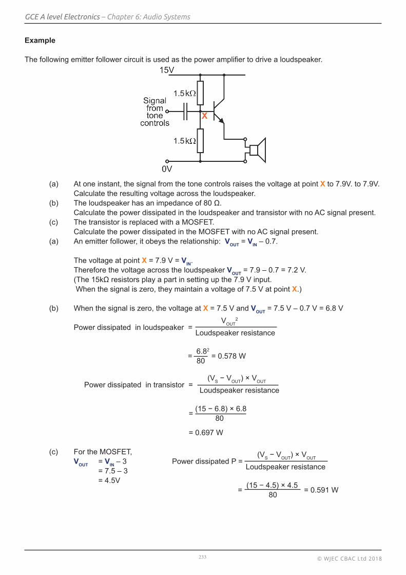
The following emitter follower circuit is used as the power amplifier to drive a loudspeaker.
(a) At one instant, the signal from the tone controls raises the voltage at point X to 7.9V. to 7.9V. Calculate the resulting voltage across the loudspeaker. (b) The loudspeaker has an impedance of 80 Ω. Calculate the power dissipated in the loudspeaker and transistor with no AC signal present. (c) The transistor is replaced with a MOSFET. Calculate the power dissipated in the MOSFET with no AC signal present. (a) An emitter follower, it obeys the relationship: VOUT = VIN – 0.7.
The voltage at point X = 7.9 V = VIN. Therefore the voltage across the loudspeaker VOUT = 7.9 – 0.7 = 7.2 V. (The 15kΩ resistors play a part in setting up the 7.9 V input. When the signal is zero, they maintain a voltage of 7.5 V at point X.)
(b) When the signal is zero, the voltage at X = 7.5 V and VOUT = 7.5 V – 0.7 V = 6.8 V
Power dissipated in loudspeaker = VOUT
2
Loudspeaker resistance
= 6.82 = 0.578 W
80
Power dissipated in transistor = (VS − VOUT) × VOUT
Loudspeaker resistance
= (15 − 6.8) × 6.8
80
= 0.697 W
(c) For the MOSFET, VOUT = VIN – 3 Power dissipated P =
(VS − VOUT) × VOUT = 7.5 – 3 Loudspeaker resistance
= 4.5V = (15 − 4.5) × 4.5 = 0.591 W 80
1.5
1.5
© WJEC CBAC Ltd 2018234
GCE A level Electronics – Chapter 6: Audio Systems
Exercise 6.5
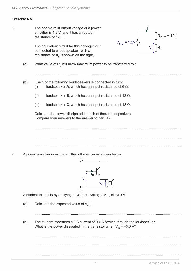
1. The open-circuit output voltage of a power amplifier is 1.2 V, and it has an output resistance of 12 Ω.
The equivalent circuit for this arrangement connected to a loudspeaker with a resistance of RL is shown on the right,. (a) What value of RL will allow maximum power to be transferred to it.
(b) Each of the following loudspeakers is connected in turn: (i) loudspeaker A, which has an input resistance of 6 Ω;
(ii) loudspeaker B, which has an input resistance of 12 Ω;
(iii) loudspeaker C, which has an input resistance of 18 Ω.
Calculate the power dissipated in each of these loudspeakers. Compare your answers to the answer to part (a).
2. A power amplifier uses the emitter follower circuit shown below.
A student tests this by applying a DC input voltage, VIN , of +3.0 V.
(a) Calculate the expected value of VOUT:
(b) The student measures a DC current of 0.4 A flowing through the loudspeaker. What is the power dissipated in the transistor when VIN = +3.0 V?
© WJEC CBAC Ltd 2018235
GCE A level Electronics – Chapter 6: Audio Systems
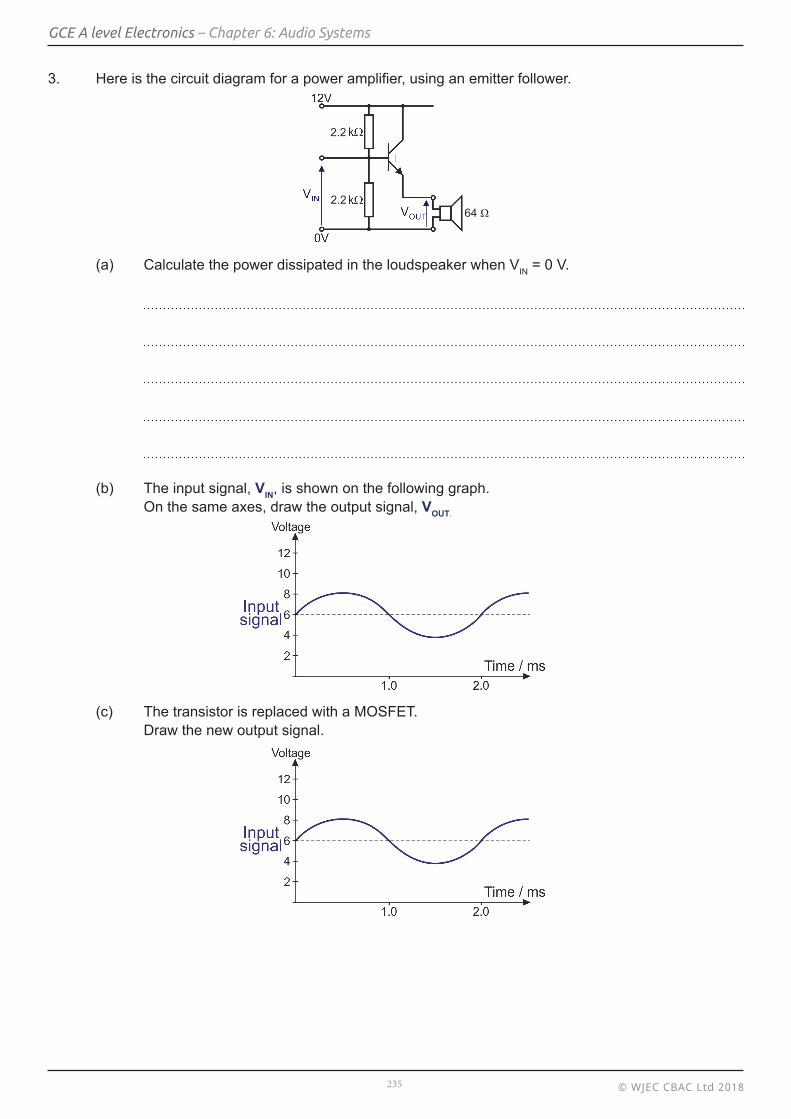
3. Here is the circuit diagram for a power amplifier, using an emitter follower.
(a) Calculate the power dissipated in the loudspeaker when VIN = 0 V.
(b) The input signal, VIN, is shown on the following graph. On the same axes, draw the output signal, VOUT.
(c) The transistor is replaced with a MOSFET. Draw the new output signal.
2.2
2.264 Ω
© WJEC CBAC Ltd 2018236
GCE A level Electronics – Chapter 6: Audio Systems
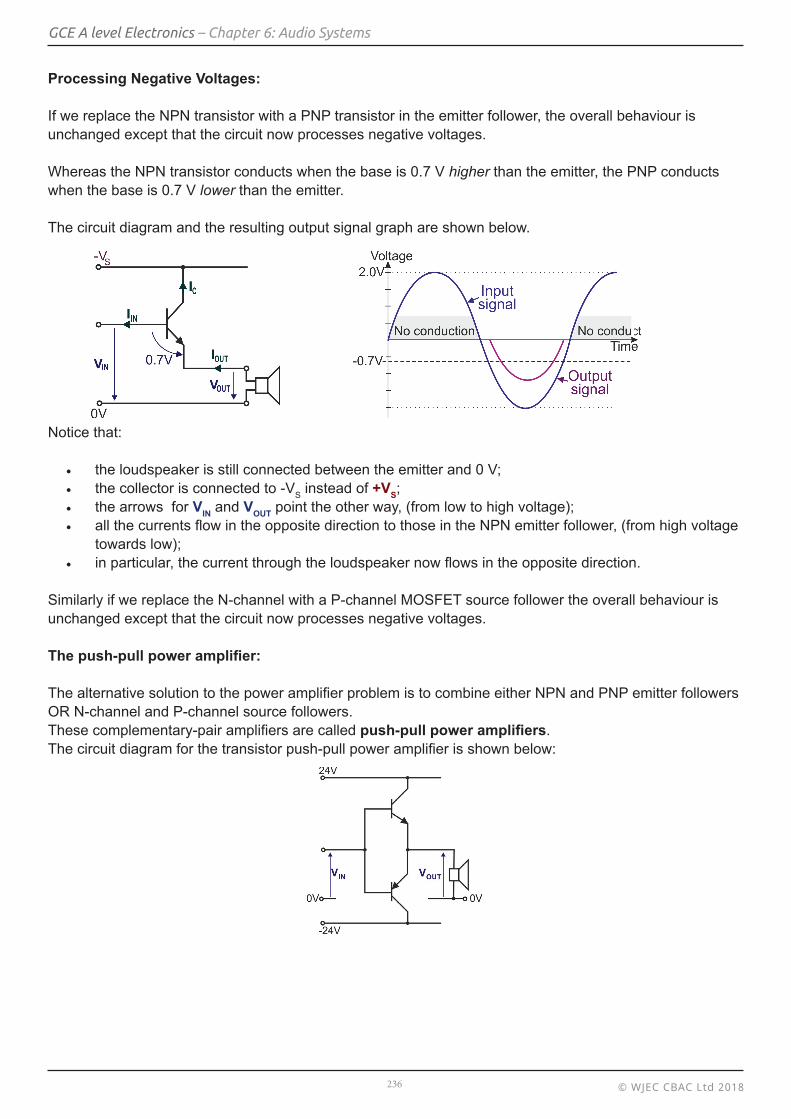
Processing Negative Voltages:
If we replace the NPN transistor with a PNP transistor in the emitter follower, the overall behaviour is unchanged except that the circuit now processes negative voltages. Whereas the NPN transistor conducts when the base is 0.7 V higher than the emitter, the PNP conducts when the base is 0.7 V lower than the emitter.
The circuit diagram and the resulting output signal graph are shown below.
Notice that:
• the loudspeaker is still connected between the emitter and 0 V;• the collector is connected to -VS instead of +VS;• the arrows for VIN and VOUT point the other way, (from low to high voltage);• all the currents flow in the opposite direction to those in the NPN emitter follower, (from high voltage
towards low);• in particular, the current through the loudspeaker now flows in the opposite direction.
Similarly if we replace the N-channel with a P-channel MOSFET source follower the overall behaviour is unchanged except that the circuit now processes negative voltages.
The push-pull power amplifier:
The alternative solution to the power amplifier problem is to combine either NPN and PNP emitter followers OR N-channel and P-channel source followers.These complementary-pair amplifiers are called push-pull power amplifiers.The circuit diagram for the transistor push-pull power amplifier is shown below:
© WJEC CBAC Ltd 2018237
GCE A level Electronics – Chapter 6: Audio Systems
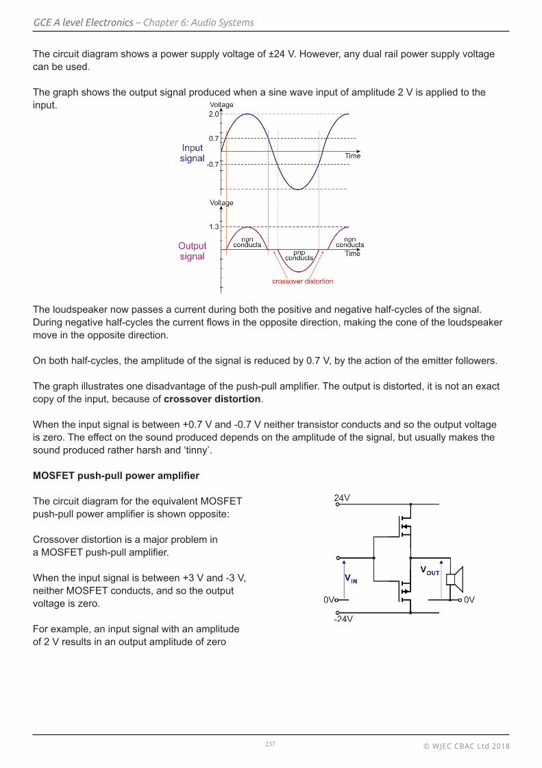
The circuit diagram shows a power supply voltage of ±24 V. However, any dual rail power supply voltage can be used.
The graph shows the output signal produced when a sine wave input of amplitude 2 V is applied to the input.
The loudspeaker now passes a current during both the positive and negative half-cycles of the signal. During negative half-cycles the current flows in the opposite direction, making the cone of the loudspeaker move in the opposite direction.
On both half-cycles, the amplitude of the signal is reduced by 0.7 V, by the action of the emitter followers.
The graph illustrates one disadvantage of the push-pull amplifier. The output is distorted, it is not an exact copy of the input, because of crossover distortion.
When the input signal is between +0.7 V and -0.7 V neither transistor conducts and so the output voltage is zero. The effect on the sound produced depends on the amplitude of the signal, but usually makes the sound produced rather harsh and ‘tinny’.
MOSFET push-pull power amplifier
The circuit diagram for the equivalent MOSFETpush-pull power amplifier is shown opposite:
Crossover distortion is a major problem ina MOSFET push-pull amplifier.
When the input signal is between +3 V and -3 V,neither MOSFET conducts, and so the outputvoltage is zero.
For example, an input signal with an amplitudeof 2 V results in an output amplitude of zero
© WJEC CBAC Ltd 2018238
GCE A level Electronics – Chapter 6: Audio Systems
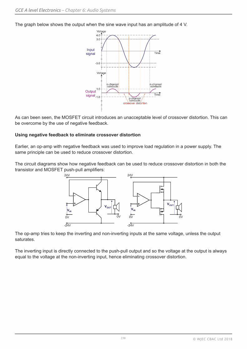
The graph below shows the output when the sine wave input has an amplitude of 4 V.
As can been seen, the MOSFET circuit introduces an unacceptable level of crossover distortion. This can be overcome by the use of negative feedback.
Using negative feedback to eliminate crossover distortion
Earlier, an op-amp with negative feedback was used to improve load regulation in a power supply. The same principle can be used to reduce crossover distortion.
The circuit diagrams show how negative feedback can be used to reduce crossover distortion in both the transistor and MOSFET push-pull amplifiers:
The op-amp tries to keep the inverting and non-inverting inputs at the same voltage, unless the output saturates.
The inverting input is directly connected to the push-pull output and so the voltage at the output is always equal to the voltage at the non-inverting input, hence eliminating crossover distortion.
© WJEC CBAC Ltd 2018239
GCE A level Electronics – Chapter 6: Audio Systems
Maximum Output PowerUsing rms values, the output power is given by:
P = VRMS
2
RL
On an oscilloscope, it is easier to measure the peak-to-peak output voltage (VP-P).The equation can be modified as follows:
POUT = VRMS
2
RL
= 1
VP
2 where VP is the peak voltage of the signal.
RL √ 2
∴ VP = VP-P
2
Hence POUT = 1
VP-P
2
RL 2√ 2
= 1
VP-P
2
RL 2√ 2
= (VP-P)2
RL
( 2√ 2)2
∴ ( 2√2 )2 = 8
POUT = VP-P
2
8RL
The maximum output power occurs when the push-pull amplifier is producing the maximumpeak-to-peak output voltage, a value equal to the power supply voltage.For a dual rail voltage supply of ±VS
PMAX = VS
2
where VS = VS+ - VS- 8RL
Limitations of using the Maximum Output Power equation• The formula is completely valid for a circuit employing op-amp negative feedback assuming the
op-amp is powered from a power supply which is a few volts greater than VS. (This is to offset the op-amp saturation values and the 0.7 V or 3 V voltage drop across the conducting transistor or MOSFET respectively).
As the op-amp power supply connections are not normally shown in a circuit diagram, you may assume that they are sufficiently high to allow maximum power when performing power calculations.• For a transistor amplifier without feedback, the equation gives a fairly accurate result when the
power supply voltage is large.• A MOSFET push-pull amplifier would be of little use without feedback so the inaccuracy of using the
formula is not an issue.
© WJEC CBAC Ltd 2018240
GCE A level Electronics – Chapter 6: Audio Systems
Example A transistor push-pull amplifier is powered by a ±30 V power supply and is connected to a 6 ± loudspeaker.Calculate the maximum output power.
Using Pmax = VS
2
8 RL
Pmax = 602
(8 x 6)
= 75 WNote:If the amplifier did not employ negative feedback then Pmax would reduce to :
58.62 = 71.5 W
(8 x 6)
As can be seen, the formula still gives a good indication of the maximum output power.
© WJEC CBAC Ltd 2018241
GCE A level Electronics – Chapter 6: Audio Systems
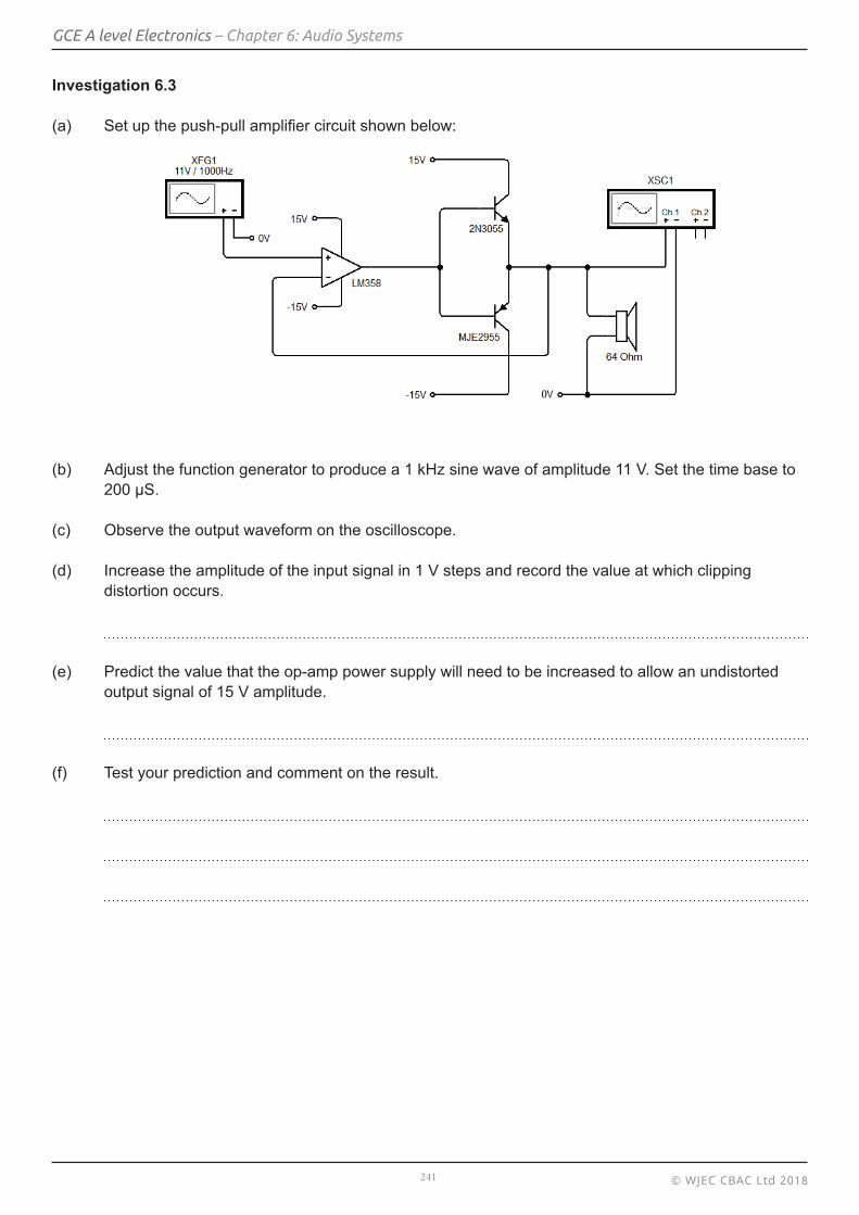
Investigation 6.3
(a) Set up the push-pull amplifier circuit shown below:
(b) Adjust the function generator to produce a 1 kHz sine wave of amplitude 11 V. Set the time base to 200 µS.
(c) Observe the output waveform on the oscilloscope.
(d) Increase the amplitude of the input signal in 1 V steps and record the value at which clipping distortion occurs.
(e) Predict the value that the op-amp power supply will need to be increased to allow an undistorted output signal of 15 V amplitude.
(f) Test your prediction and comment on the result.
© WJEC CBAC Ltd 2018242
GCE A level Electronics – Chapter 6: Audio Systems
Exercise 6.6 1. A transistor push-pull amplifier connected to a ±24 V power supply. Calculate the minimum power rating for a 6 Ω loudspeaker connected to it.
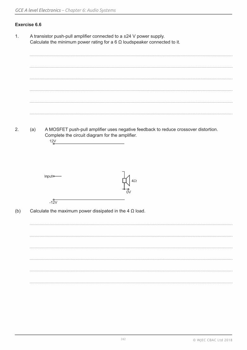
2. (a) A MOSFET push-pull amplifier uses negative feedback to reduce crossover distortion. Complete the circuit diagram for the amplifier.
(b) Calculate the maximum power dissipated in the 4 Ω load.
© WJEC CBAC Ltd 2018243
GCE A level Electronics – Chapter 6: Audio Systems
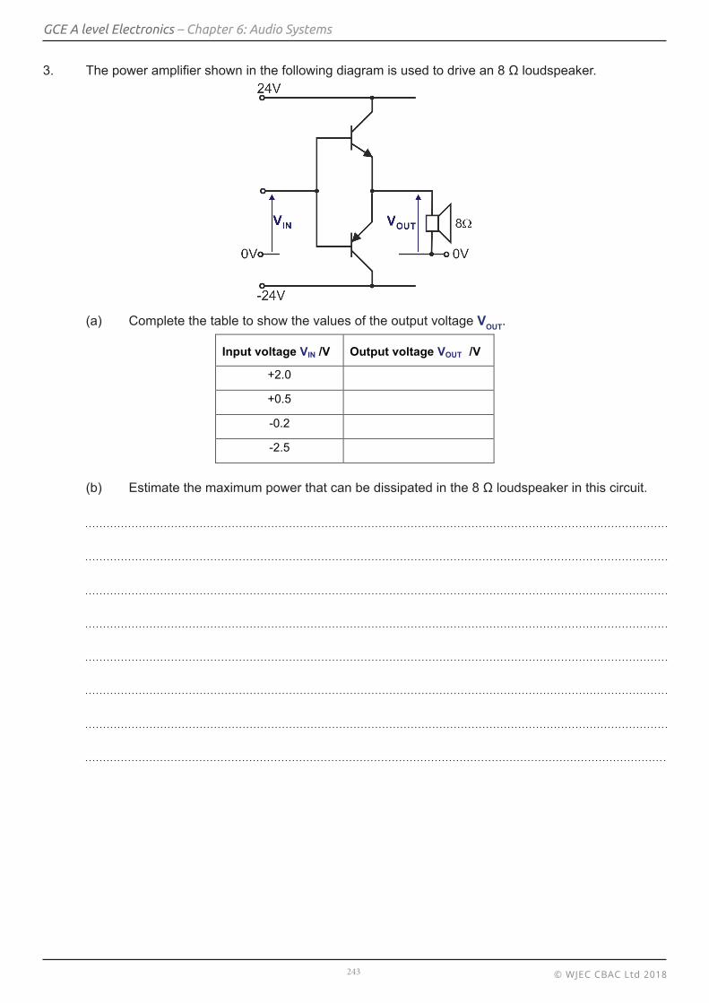
3. The power amplifier shown in the following diagram is used to drive an 8 Ω loudspeaker.
(a) Complete the table to show the values of the output voltage VOUT.
(b) Estimate the maximum power that can be dissipated in the 8 Ω loudspeaker in this circuit.
Input voltage VIN /V
Output voltage VOUT /V
+2.0
+0.5
-0.2
-2.5
© WJEC CBAC Ltd 2018244
GCE A level Electronics – Chapter 6: Audio Systems
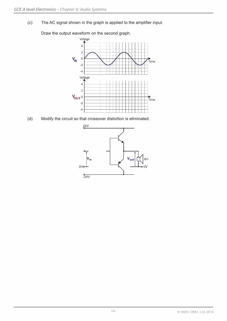
(c) The AC signal shown in the graph is applied to the amplifier input.
Draw the output waveform on the second graph.
(d) Modify the circuit so that crossover distortion is eliminated.