Embed Size (px)
Citation preview
102
CHAPTER 5
IMPLEMENTATION OF FIVE LEVEL CASCADED
MULTILEVEL INVERTER AND HARDWARE RESULTS
5.1 INTRODUCTION
In the last decade the study on the multilevel inverters has becoming
the emerging research topic at simulation level using various simulation tools
for various topologies and levels. Thanks to the recent advancement on digital
processors and power semiconductor devices the hardware realization is
possible for the verification of the performance of the simulated systems. This
section presents the hardware implementation of the three phase five level
cascaded multilevel inverter fed induction motor drive test setup for
experimentations. With the development of power electronic devices like the
Insulated Gate Bipolar Transistor (IGBT), the power MOSFET and the
advances in processors, the AC induction motor is becoming popular in
variable speed drives with different modulation drive circuits. Since the rise
time and fall time of the IGBT’s are less than 200ns, the dissipation loss
across the device becomes very less, which improves the performance of the
power electronic converter system. However due to the fast switching action
of the device the dv/dt of the inverter output becomes large and this can be
reduced with the increased power levels discussed in Renge et al (2008) and
Leppanen et al (2006).
There are several steps involved in implementing the hardware.
Basically any power electronic system is divided into two of which one is the
103
control unit and the other is the power unit. The control unit consists of pulse
generation circuit, driver circuit and isolation circuit. The power unit consists
of input supply unit and the power processing unit.
In order to verify the performance of the simulated system The
proposed five level cascaded multilevel inverter fed induction motor drive is
implemented with IGBTs as switching elements and is tested with the three
phase 440 Volts squirrel cage induction motor coupled loading arrangements.
In modern electric drives high performance control is needed which can be easily
achieved using advanced digital processors. The open loop V/f control based on
multilevel proposed Space Vector PWM is implemented on Xilinx Spartan
XC3S400 FPGA processor. Gating signals are generated for the fundamental
output frequency of 50Hz and side bands of 40Hz and 45Hz.
5.2 HARDWARE SPECIFICATIONS
The complete hardware specification of the proposed system is as
follows
Multilevel Inverter Input and Output Supply:
• Storage Batteries with the combination of producing 72V
output DC.
• Isolated photovoltaic panels with 72V (3x24V) output DC.
• The input DC is 432V (6x72V)
• Desired output 5kVA,output voltage 415V,output current
(Max)10A,
• Output frequency 40-50Hz, Three Phase AC supply confined
to IEEE standards.
104
5.3 HARDWARE IMPLEMENTATION
The proposed control algorithm is generated in front end with the
aid of system generator editor, the SVPWM blocks with necessary
transformation equations and the associated blocks for individual phases are
interconnected and the sampling frequency is set to 5kHz. The entire control
algorithm with sampling rate of 5kHz which is based on proposed SVPWM
algorithm is implemented in the system generator environment and
corresponding code for FPGA processor is generated. The generated code is
downloaded into the digital processor Xilinx Spartan 3A XC3S400 and
hardware settings are enabled such that the output SVPWM pulses are
available at the output ports.
5.3.1 Protection Circuit for Integration for FPGA Integration
The voltage levels of any CMOS based digital processors are in the
order of 3.3V to 3.5V DC. This voltage levels are sufficient to turn ON the
modern smart Insulated Gate Bipolar Transistor (IGBTs). The smart power
modules has inbuilt driver circuit. Here the power switches used are Fair
Child make smart power module FCAS50SN60 which is rated for 600V, 50A,
though it is rated for higher ratings it is operated for nominal three phase
voltage range and with a load of less than 5A, it is an advanced smart power
module for motor drives that has newly developed and designed to provide
very compact and high performance motor drives. Switching frequency of
power switch is in between 2.2 and 8 kHz. It combines optimized circuit
protection and drive matched to low loss IGBTs. System reliability is further
enhanced by the integrated under voltage lock out and short circuit protection.
In addition the incorporated HVIC facilitates, the use of single supply drive
topology enabling FCAS50SN60 to be driven by only one drive supply
voltage without negative bias. Each phase current of inverter can be
monitored separately due to the divided negative DC terminals. The entire
105
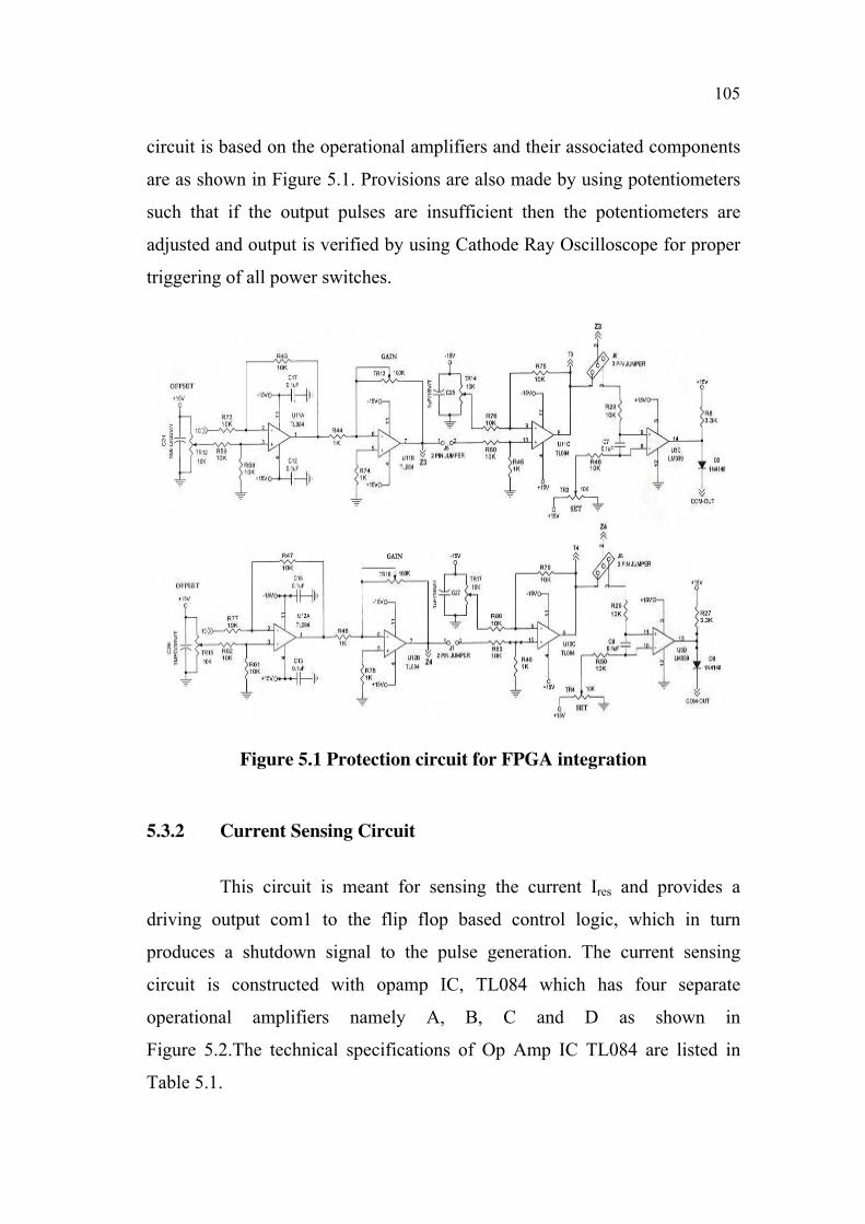
circuit is based on the operational amplifiers and their associated components
are as shown in Figure 5.1. Provisions are also made by using potentiometers
such that if the output pulses are insufficient then the potentiometers are
adjusted and output is verified by using Cathode Ray Oscilloscope for proper
triggering of all power switches.
Figure 5.1 Protection circuit for FPGA integration
5.3.2 Current Sensing Circuit
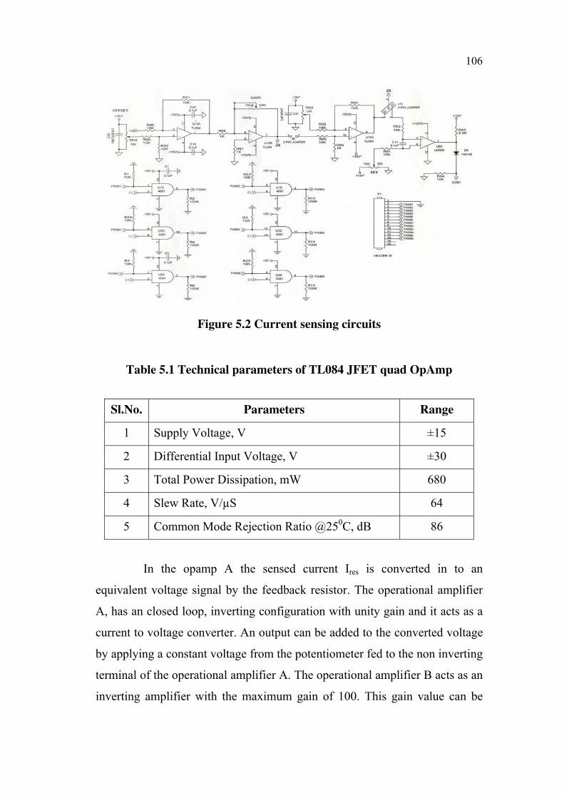
This circuit is meant for sensing the current Ires and provides a
driving output com1 to the flip flop based control logic, which in turn
produces a shutdown signal to the pulse generation. The current sensing
circuit is constructed with opamp IC, TL084 which has four separate
operational amplifiers namely A, B, C and D as shown in
Figure 5.2.The technical specifications of Op Amp IC TL084 are listed in
Table 5.1.
106
Figure 5.2 Current sensing circuits
Table 5.1 Technical parameters of TL084 JFET quad OpAmp
Sl.No. Parameters Range
1 Supply Voltage, V ±15
2 Differential Input Voltage, V ±30
3 Total Power Dissipation, mW 680
4 Slew Rate, V/µS 64
5 Common Mode Rejection Ratio @250C, dB 86
In the opamp A the sensed current Ires is converted in to an
equivalent voltage signal by the feedback resistor. The operational amplifier
A, has an closed loop, inverting configuration with unity gain and it acts as a
current to voltage converter. An output can be added to the converted voltage
by applying a constant voltage from the potentiometer fed to the non inverting
terminal of the operational amplifier A. The operational amplifier B acts as an
inverting amplifier with the maximum gain of 100. This gain value can be

107
adjusted by a variable feedback resistor. This stage take cares the correction
of 1800 inversion produced by the previous stage.
The operational amplifier C is in non inverting, unity gain
configuration. The amplified output voltage from stage B is normalized using
a potential divider at the input to the non inverting terminal. The inverting
terminal houses an additional adjustment with a negative voltage fed through
a potentiometer.
The operational amplifier D is in open loop configuration and acts
as a comparator. The output signal COM1 is fired whenever the sensed
current Ires exceeds a limiting value. This limiting value can be adjusted, by
the available trim potentiometer arrangement providing input to the non
inverting terminal of this opamp D. The diode at the output D avails
protection to the next stage circuit.
5.3.3 Isolation Circuit
In any power electronics system the main problem is isolating the
power circuit from the control circuit. There are many situations where
signals and data need to be transferred from one subsystem to another within
a piece of electronics equipment, or from one piece of equipment to another,
without making a direct Ohmic electrical connection. Often this is because the
source and destination are (or may be at times) at very different voltage
levels, like a microprocessor which is operating from 5V DC but being used
to control any power switches which is switching 240V AC. In such situations
the link between the two must be an isolated one, to protect the
microprocessor from overvoltage damage. Relays can of course provide this
kind of isolation, but even small relays tend to be fairly bulky compared with
ICs and many of today’s other miniature circuit components. Because they are
electro-mechanical, it is not reliable and suitable for relatively low speed
operation. Where small size, higher speed and greater reliability are required,
108
a much better alternative is to use opto isolator. It uses a beam of light to
transmit the signals or data across an electrical barrier, and achieve excellent
isolation.
In case of power circuit the operating voltage is in the order of
hundreds of Volts to several kV, due to any short circuits on the power circuit
there may be a chance of feeding the high voltages to the low power control
circuitry which usually operates in the order of 5V or so. The commonly used
isolation circuits are isolation transformers and opto isolators. A common
implementation of an opto isolation circuit is a LED and a phototransistor in a
light tight housing to exclude ambient light and without common electrical
connection, positioned so that light from the LED will impinge on the photo
detector. When an electrical signal is applied to the input of the opto isolator,
its LED lights and illuminates the photo detector, producing a corresponding
electrical signal in the output circuit. With a photodiode as the detector, the
output current is proportional to the intensity of incident light supplied by the
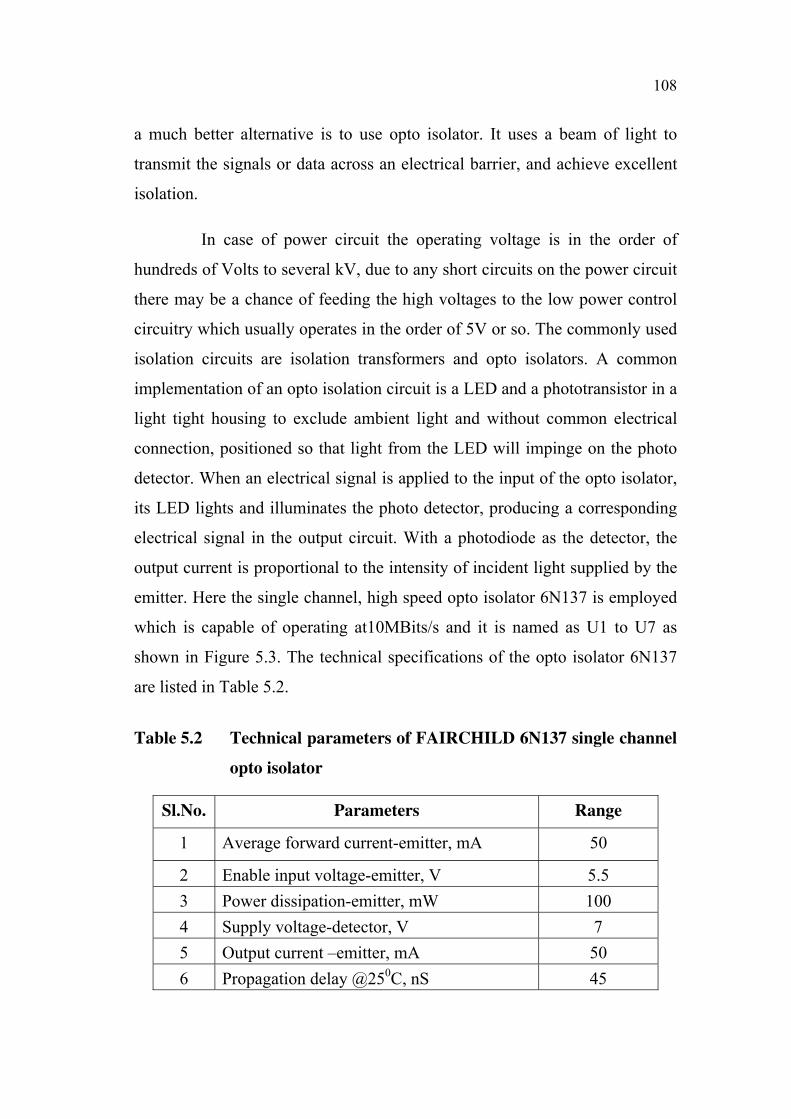
emitter. Here the single channel, high speed opto isolator 6N137 is employed
which is capable of operating at10MBits/s and it is named as U1 to U7 as
shown in Figure 5.3. The technical specifications of the opto isolator 6N137
are listed in Table 5.2.
Table 5.2 Technical parameters of FAIRCHILD 6N137 single channel
opto isolator
Sl.No. Parameters Range
1 Average forward current-emitter, mA 50
2 Enable input voltage-emitter, V 5.5
3 Power dissipation-emitter, mW 100
4 Supply voltage-detector, V 7
5 Output current –emitter, mA 50
6 Propagation delay @250C, nS 45
109
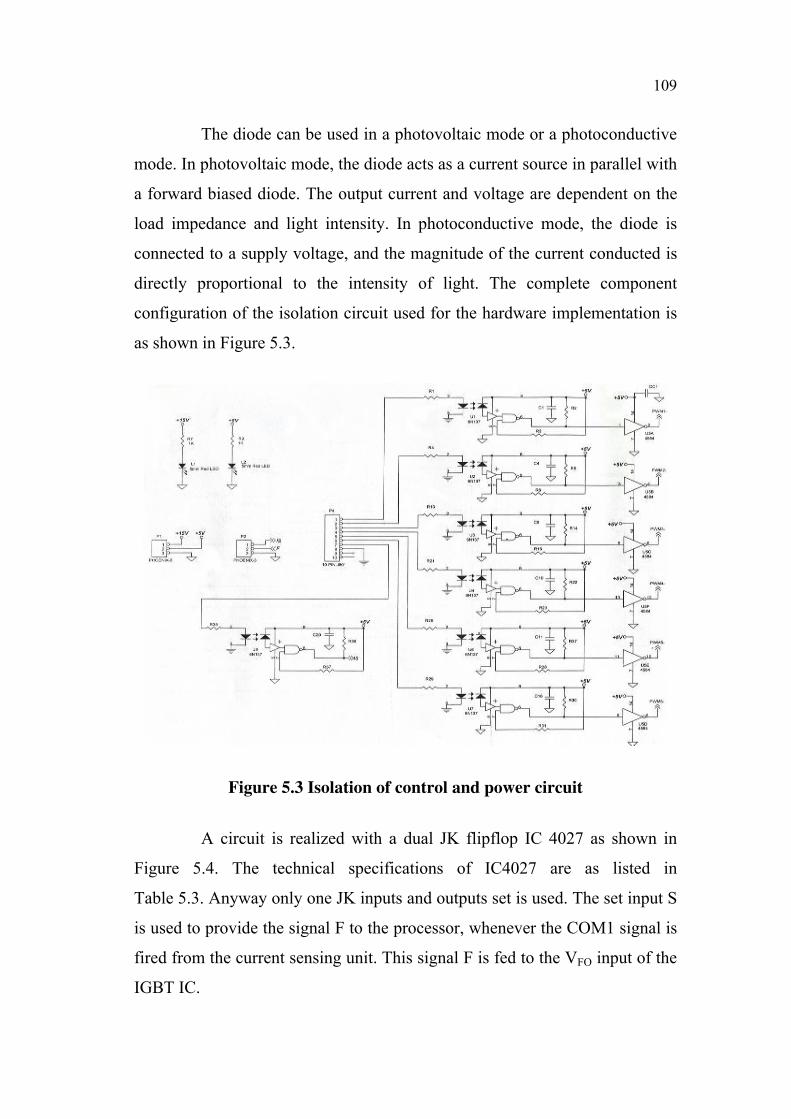
The diode can be used in a photovoltaic mode or a photoconductive
mode. In photovoltaic mode, the diode acts as a current source in parallel with
a forward biased diode. The output current and voltage are dependent on the
load impedance and light intensity. In photoconductive mode, the diode is
connected to a supply voltage, and the magnitude of the current conducted is
directly proportional to the intensity of light. The complete component
configuration of the isolation circuit used for the hardware implementation is
as shown in Figure 5.3.
Figure 5.3 Isolation of control and power circuit
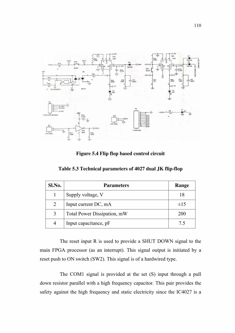
A circuit is realized with a dual JK flipflop IC 4027 as shown in
Figure 5.4. The technical specifications of IC4027 are as listed in
Table 5.3. Anyway only one JK inputs and outputs set is used. The set input S
is used to provide the signal F to the processor, whenever the COM1 signal is
fired from the current sensing unit. This signal F is fed to the VFO input of the
IGBT IC.
110
Figure 5.4 Flip flop based control circuit
Table 5.3 Technical parameters of 4027 dual JK flip-flop
Sl.No. Parameters Range
1 Supply voltage, V 18
2 Input current DC, mA ±15
3 Total Power Dissipation, mW 200
4 Input capacitance, pF 7.5
The reset input R is used to provide a SHUT DOWN signal to the
main FPGA processor (as an interrupt). This signal output is initiated by a
reset push to ON switch (SW2). This signal is of a hardwired type.
The COM1 signal is provided at the set (S) input through a pull
down resistor parallel with a high frequency capacitor. This pair provides the
safety against the high frequency and static electricity since the IC4027 is a
111
CMOS IC. The COM1 signal which is produced whenever Is exceeds a limit,
is used to produce signal F1. Direct switch reset by SW2, produces the
shutdown signal. The COM OUT and SHUTDOWN signals are fed to another
set input of IC 4027 through wired AND gate which produces F2. The reset R
input of IC4027 produces signal C1, by the input RST3.
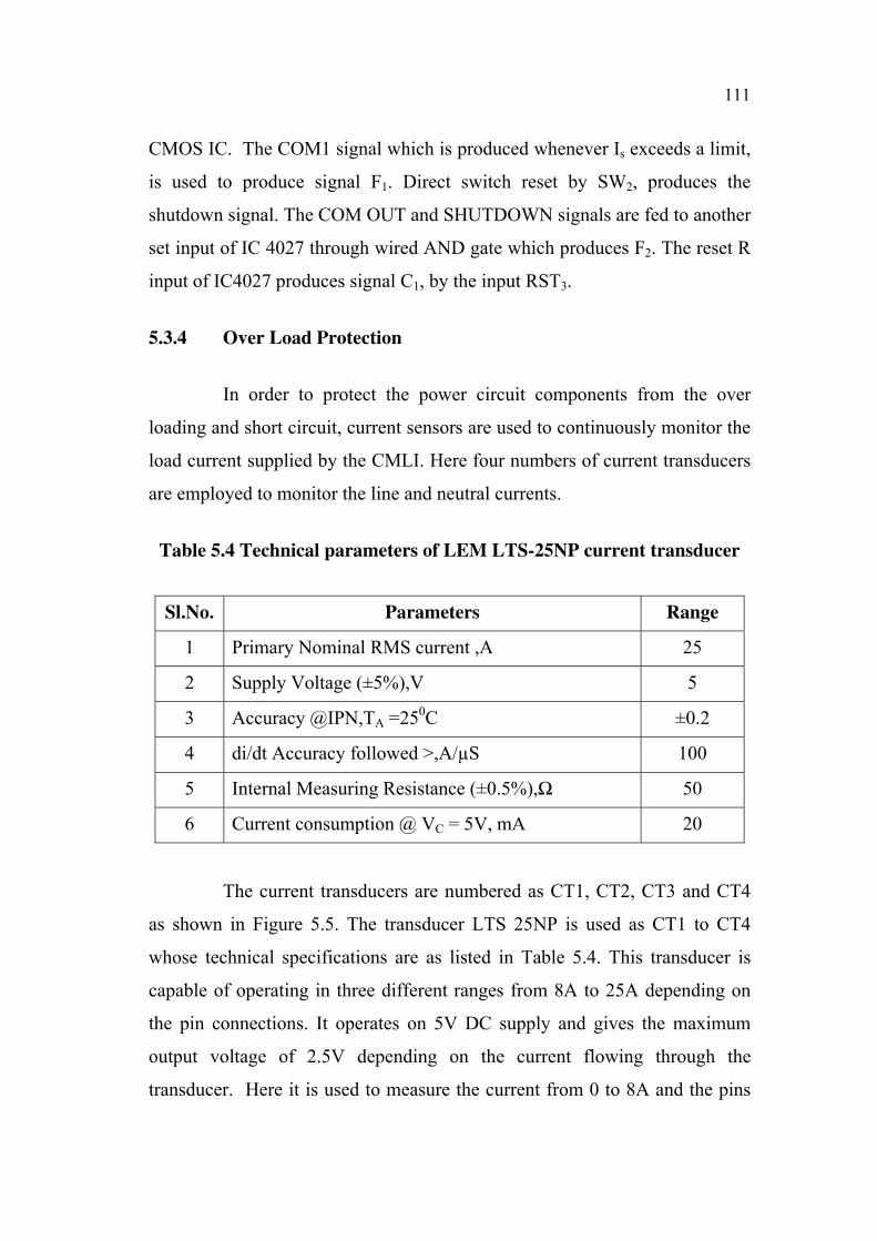
5.3.4 Over Load Protection
In order to protect the power circuit components from the over
loading and short circuit, current sensors are used to continuously monitor the
load current supplied by the CMLI. Here four numbers of current transducers
are employed to monitor the line and neutral currents.
Table 5.4 Technical parameters of LEM LTS-25NP current transducer
Sl.No. Parameters Range
1 Primary Nominal RMS current ,A 25
2 Supply Voltage (±5%),V 5
3 Accuracy @IPN,TA =250C ±0.2
4 di/dt Accuracy followed >,A/µS 100
5 Internal Measuring Resistance (±0.5%),Ω 50
6 Current consumption @ VC = 5V, mA 20
The current transducers are numbered as CT1, CT2, CT3 and CT4
as shown in Figure 5.5. The transducer LTS 25NP is used as CT1 to CT4
whose technical specifications are as listed in Table 5.4. This transducer is
capable of operating in three different ranges from 8A to 25A depending on
the pin connections. It operates on 5V DC supply and gives the maximum
output voltage of 2.5V depending on the current flowing through the
transducer. Here it is used to measure the current from 0 to 8A and the pins
112
are connected accordingly. Pin 1 is used as input and the pin 4 is used as
output. For 8A measurement pin 3 and 5, 2 and 6 are short circuited. This
gives the complete protection for power circuit and protects the power devices
against overload. The complete overload protection circuit arrangement is as
shown in Figure 5.4
Figure 5.5 LEM current sensors for overload/over current protection
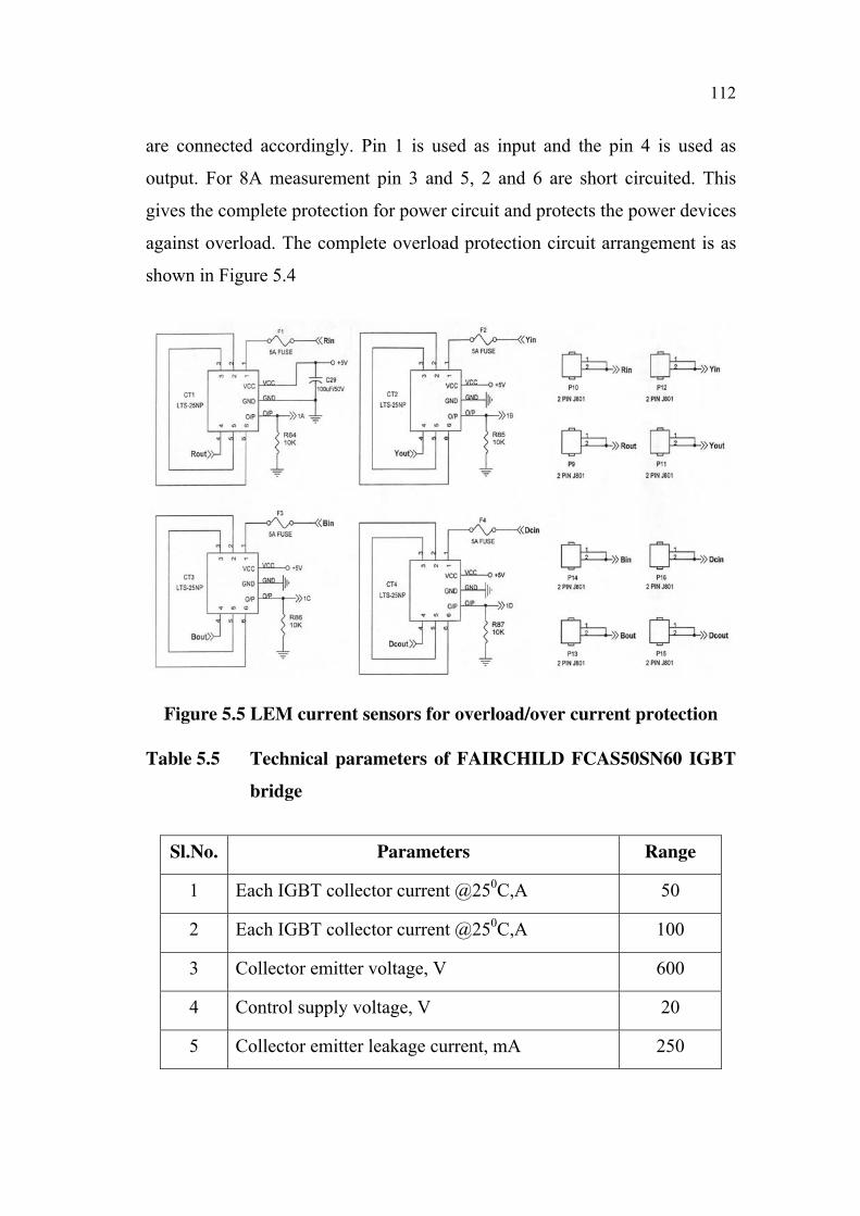
Table 5.5 Technical parameters of FAIRCHILD FCAS50SN60 IGBT
bridge
Sl.No. Parameters Range
1 Each IGBT collector current @250C,A 50
2 Each IGBT collector current @250C,A 100
3 Collector emitter voltage, V 600
4 Control supply voltage, V 20
5 Collector emitter leakage current, mA 250

113
Figure 5.6 Connection circuit for FCAS50SN60 IGBT smart power
module
5.3.5 Photographs of Integrated Hardware Unit
After the modular design of various units, each module was tested
individually and the pulse patterns are verified with the digital storage
oscilloscopes and integrated to achieve the stated performance on the output
of the system. Figure 5.7 shows the photograph of the complete hardware
setup after the integration of amplification circuit, isolation circuit and power
circuit for the three phase five level cascaded multilevel inverter. Since the
inverter system is to operate the induction motor drive at the current rating
less than 5A hence the natural cooling of power device is employed with heat
sinks. Figure 5.8 shows the photograph of an FPGA processor which is used
for pulse generations.

114
Figure 5.7 Photograph of complete hardware of three phase five level
CMLI
Figure 5.8 Photograph of FPGA processor used for proposed SVPWM
pulse generation
115
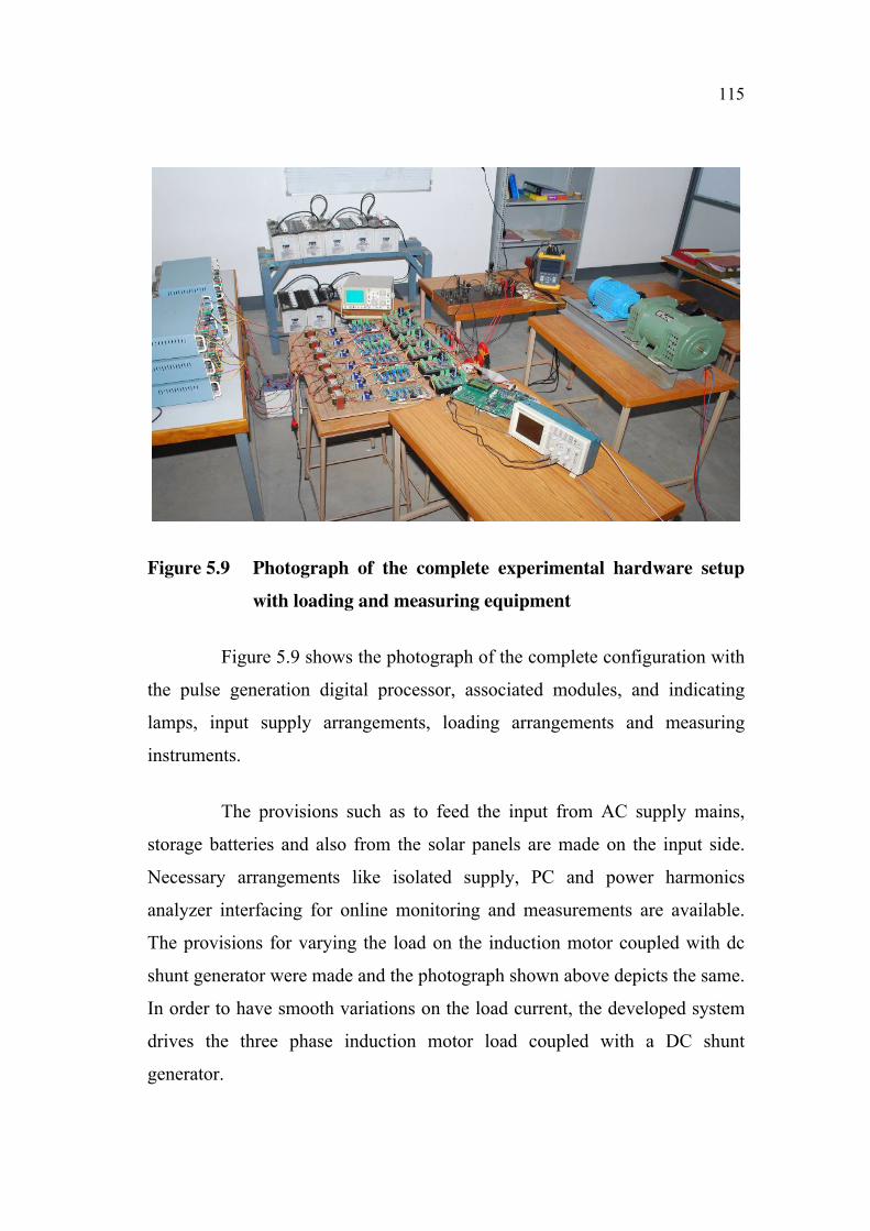
Figure 5.9 Photograph of the complete experimental hardware setup
with loading and measuring equipment
Figure 5.9 shows the photograph of the complete configuration with
the pulse generation digital processor, associated modules, and indicating
lamps, input supply arrangements, loading arrangements and measuring
instruments.
The provisions such as to feed the input from AC supply mains,
storage batteries and also from the solar panels are made on the input side.
Necessary arrangements like isolated supply, PC and power harmonics
analyzer interfacing for online monitoring and measurements are available.
The provisions for varying the load on the induction motor coupled with dc
shunt generator were made and the photograph shown above depicts the same.
In order to have smooth variations on the load current, the developed system
drives the three phase induction motor load coupled with a DC shunt
generator.

116
5.4 SPECIFICATIONS OF THE ELECTRICAL MACHINES
USED FOR TESTING OF HARDWARE
For the testing and experimentation of the proposed scheme, a
1.5kW squirrel cage induction motor is fed from the inverter with a constant
V/f ratio in open loop. The motor operates under no load, and with the
parameters given in Table 5.2. Vdc is taken as 0.432kV (6x72V). The steady
state phase voltages, phase currents and symmetry of phase voltages along
with their harmonic spectrum are analyzed for the output frequency from 40
to 50 Hz and motor is accelerated to the rated speed using an open-loop V/f
operation. For all the frequency of operation, the output voltage in each phase
varies from zero to rated voltage, and switching happens with the proposed
SVPWM technique implemented in FPGA processor.
The specifications of the AC motor and the DC machine used for
testing of the hardware setup are as shown in the Table 5.6 and 5.7
respectively.
Table 5.6 Technical parameters of the AC motor used as load for the
developed multilevel inverter
S.No. Parameters Values
1 Motor Type Induction Motor
2 No. of phases Three Phase
3 Connection Star
4 Rated Power 1.5kW
5 Rated Voltage 415V
6 Rated Current 3.35A
7 Rated Frequency 50Hz
8 Duty Cycle S1
9 Rated Speed 1400RPM
10 No. of Poles 4
11 Rs, Ls 3.69Ω, 0.26H
12 Make Kirlosakar
117
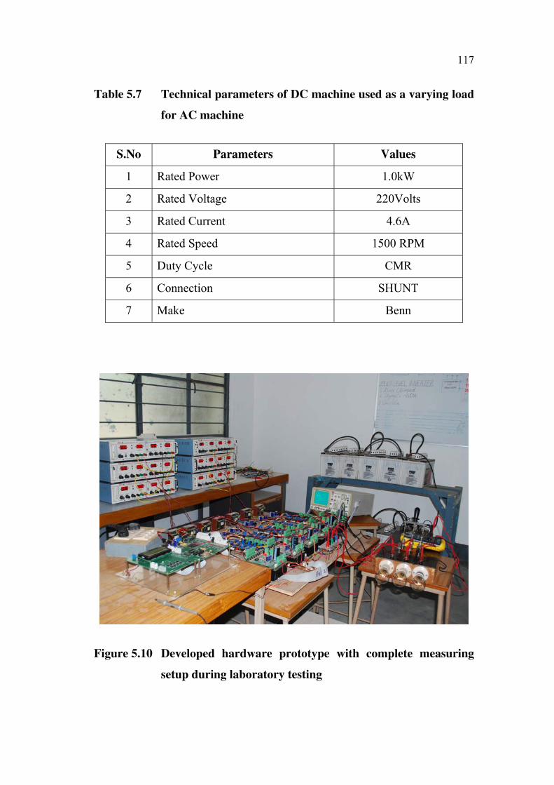
Table 5.7 Technical parameters of DC machine used as a varying load
for AC machine
S.No Parameters Values
1 Rated Power 1.0kW
2 Rated Voltage 220Volts
3 Rated Current 4.6A
4 Rated Speed 1500 RPM
5 Duty Cycle CMR
6 Connection SHUNT
7 Make Benn
Figure 5.10 Developed hardware prototype with complete measuring
setup during laboratory testing
118
5.5 TESTING OF THE MULTILEVEL INVERTER UNIT WITH
FLUKE 434 PQ ANALYZER
After testing and commissioning of the hardware unit, it is subjected
to the various experimentations under different loading conditions on its
output with the power harmonic analyzer. In order to load the three phase
induction motor in a uniform manner a DC machine is operated as a self
excited shunt generator and it is mechanically coupled to it. The DC generator
is loaded with the resistive load and this setup constitutes the loading
arrangements. This setup provides a linear load variation on the inverter side
and the performance parameters such as terminal voltage, voltage and current
harmonics levels and symmetry of three phase voltages for frequencies 40Hz,
45Hz and 50Hz are obtained with the Fluke make three phase power quality
analyzer. Here the Fluke 434 model is used, it is a three phase power quality
analyzer, and it complies with the following international standards,
ANSI/ISA S82.01-1994, EN/IEC61010-1 2nd edition 1000V measurement
category III, 600V Measurement Cat IV, Pollution degree 2, CAN/CSA-
C22.2 No.61010-1-04. The power quality analyzer configuration used for the
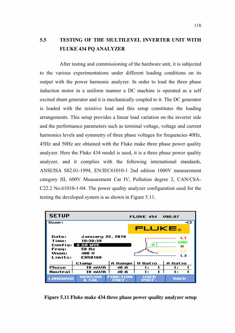
testing the developed system is as shown in Figure 5.11.
Figure 5.11 Fluke make 434 three phase power quality analyzer setup

119
Figure 5.12 Calibration and version setup of Fluke 434 power quality
analyzer
Since the three phase motor stator windings are star connected and
hence the three phase four wire system is selected, a lamp load is also used in
parallel with the motor load. The nominal voltage is 400V, the voltage and
current probes are set with the limits as shown in Figure 5.11.
Figure 5.13 Power quality analyzer setup limits page for EN50160
standard

120
The limits for the various power quality issues are set in accordance
with the standard EN50160 and range of values are as shown in Figure 5.13.
The developed system is connected to the ac motor i.e. loading arrangements
and the readings are obtained by using power quality analyzer in the scope
mode and the three phase output voltage waveform is as shown in Figure 5.14
for the set frequency of 50Hz on the digital processor. The output voltages in
all the phases i.e. RYB are 396V and the phases are 1200 apart from each
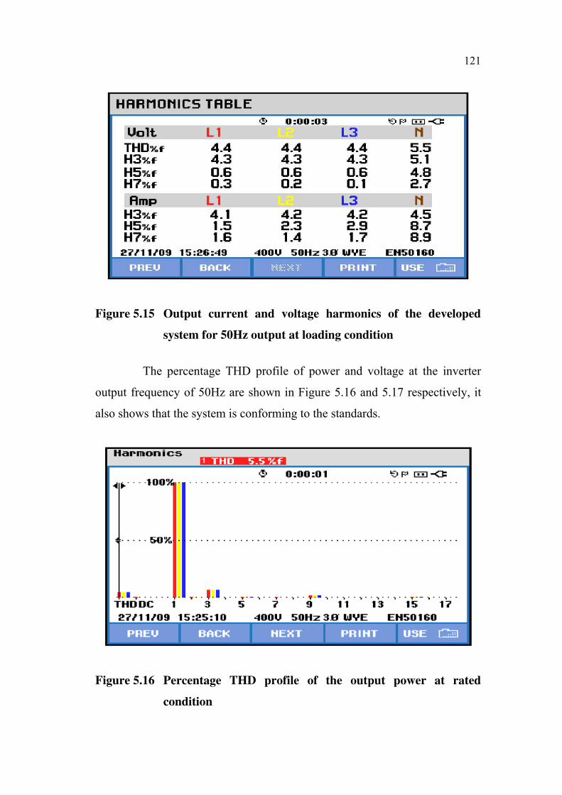
other. The neutral potential is within the prescribed limits. The output voltage
and the current harmonics are also listed in the harmonics table of the PQ
analyzer as shown in Figure 5.15. The table shows that the harmonics are very
well within the limits of the power quality standards and hence the developed
system performance is at par with the standards prescribed for power quality
issues.
Figure 5.14 Three phase output voltage waveforms for 50Hz output
121
Figure 5.15 Output current and voltage harmonics of the developed
system for 50Hz output at loading condition
The percentage THD profile of power and voltage at the inverter
output frequency of 50Hz are shown in Figure 5.16 and 5.17 respectively, it
also shows that the system is conforming to the standards.
Figure 5.16 Percentage THD profile of the output power at rated
condition
122
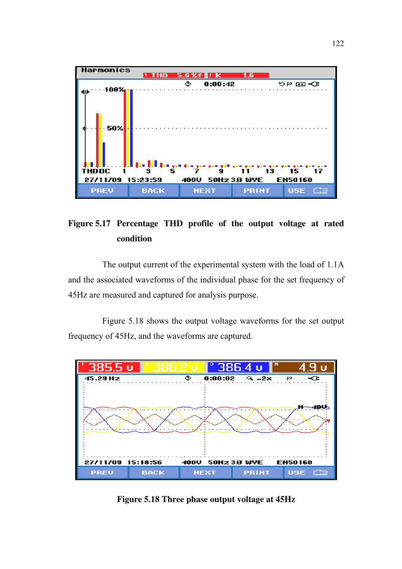
Figure 5.17 Percentage THD profile of the output voltage at rated
condition
The output current of the experimental system with the load of 1.1A
and the associated waveforms of the individual phase for the set frequency of
45Hz are measured and captured for analysis purpose.
Figure 5.18 shows the output voltage waveforms for the set output
frequency of 45Hz, and the waveforms are captured.
Figure 5.18 Three phase output voltage at 45Hz
123
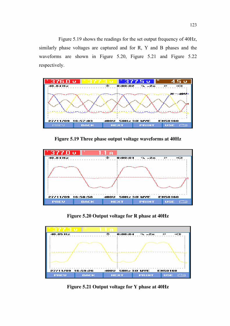
Figure 5.19 shows the readings for the set output frequency of 40Hz,
similarly phase voltages are captured and for R, Y and B phases and the
waveforms are shown in Figure 5.20, Figure 5.21 and Figure 5.22
respectively.
Figure 5.19 Three phase output voltage waveforms at 40Hz
Figure 5.20 Output voltage for R phase at 40Hz
Figure 5.21 Output voltage for Y phase at 40Hz
124
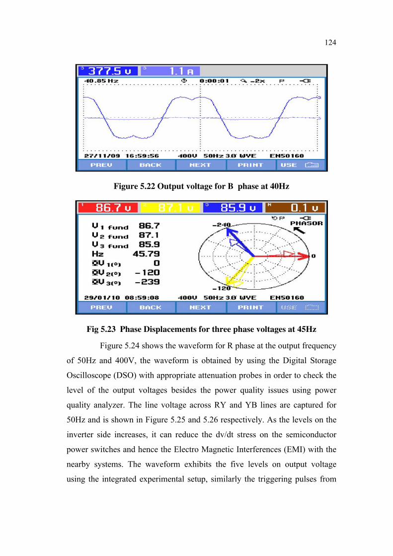
Figure 5.22 Output voltage for B phase at 40Hz
Fig 5.23 Phase Displacements for three phase voltages at 45Hz
Figure 5.24 shows the waveform for R phase at the output frequency
of 50Hz and 400V, the waveform is obtained by using the Digital Storage
Oscilloscope (DSO) with appropriate attenuation probes in order to check the
level of the output voltages besides the power quality issues using power
quality analyzer. The line voltage across RY and YB lines are captured for
50Hz and is shown in Figure 5.25 and 5.26 respectively. As the levels on the
inverter side increases, it can reduce the dv/dt stress on the semiconductor
power switches and hence the Electro Magnetic Interferences (EMI) with the
nearby systems. The waveform exhibits the five levels on output voltage
using the integrated experimental setup, similarly the triggering pulses from

125
the FPGA for the power switches are captured using the DSO is shown in
Figure 5.27.
Figure 5.24 Output Voltage Waveform for R Phase at Rated Condition
Captured Using Tektronics DSO TDS2002
Figure 5.25 Line voltage across RY for 50 Hz output
Figure 5.26 Line voltage across YB for 50 Hz output
126
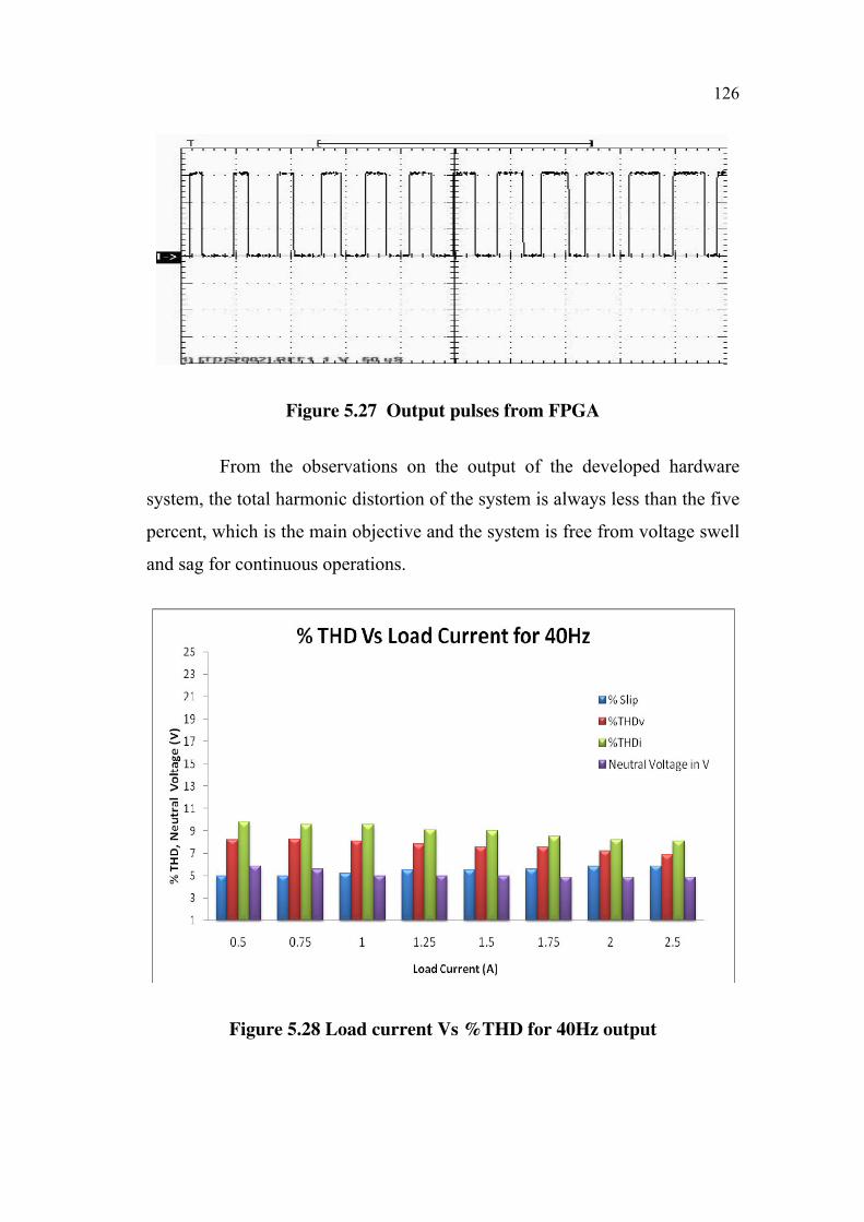
Figure 5.27 Output pulses from FPGA
From the observations on the output of the developed hardware
system, the total harmonic distortion of the system is always less than the five
percent, which is the main objective and the system is free from voltage swell
and sag for continuous operations.
Figure 5.28 Load current Vs %THD for 40Hz output
127
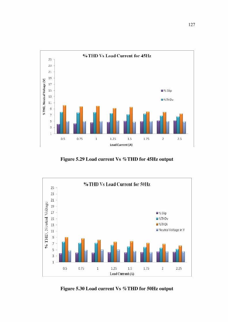
Figure 5.29 Load current Vs %THD for 45Hz output
Figure 5.30 Load current Vs %THD for 50Hz output
128
During experimentation the neutral potential, THD on the output
voltage and current are obtained continuously for different loadings and the
values are tabulated. From the obtained values the graphs were plotted for
different output frequency of 40Hz, 45Hz and 50Hz and shown in Figure
5.28, 5.29 and 5.30 respectively.
5.6 CONCLUSION
The implementation and testing of a low cost FPGA based
cascaded multilevel inverter for induction motor drive was carried out. The
main advantage of this is the ability to generate SVPWM waveform in real
time using control algorithm in the Xilinx processor. This reduces the
computational time required to determine the switching times for inverter
legs, making the system more suitable for real time implementation for larger
drives. This FPGA based cascaded multilevel inverter finds wide application
where power quality issues are the major considerations. Furthermore during
the testing of the output of the developed experimental setup with the Fluke
434 model, the three phase power quality analyzer shows that the results
exhibit the good quality of output waveforms with higher fundamental
frequency component. Also the power quality issues are very well within the
prescribed limits.
The results from the experimental setup show the output waveforms
with reduced percentage THD. The higher fundamental frequency component
on output results in reduced switching losses in semiconductor switches as
well as power loss on the motor drive. With these results it can be concluded
that the conventional drives with two level inverters can be replaced by
multilevel inverter where ever it is possible in order to maintain the good
quality of the power.