Embed Size (px)
Citation preview
48
Chapter 4 High Mobility in Modulation-Doped Si
Two-Dimensional Electron Gases
4.1 Introduction
The two-dimensional electron gas (2DEG) in semiconductors is a fundamental
low-dimensional system [63] for condensed matter physics. Important physical
phenomena such as the integral and the fractional quantum Hall effects were discovered
in high-quality 2DEGs [64, 65]. Furthermore, practical applications such as
modulation-doped field-effect transistors (MODFETs) [66] or quantum computation [12]
were also realized by utilizing a 2DEG. The most important feature of a 2DEG is its high
electron mobility using the so-called modulation-doping technique to separate the
supply impurities and electrons [67]. A record high mobility of 3.5 107 cm2/V-s was
demonstrated in a GaAs 2DEG at T < 1 K [68]. In silicon, the electron confinement
could be achieved in the inversion layer of Si MOS structure [64]. However, strong
scattering from the impurity charges of the Si/SiO2 interface has restricted the electron
mobility to the level of 2 104 cm2/V-s [69].
In 1985, Abstreiter et al. showed that electrons can be confined in a strained Si
layer sandwiched between the relaxed SiGe layers [70]. In their Si/SiGe heterostructure,
the mobility was fairly low (~2000 cm2/V-s) due to the high density of dislocation
defects by a large lattice mismatch between Si and SiGe layers. With a thick graded
Si1-xGex layer (0 < x < 0.3) of several microns grown on a Si substrate followed by a
49
relaxed Si0.7Ge0.3 layer, Ismail et al. demonstrated a much improved mobility of 535,000
cm2/V-s [71]. A yet higher electron mobility of 800,000 cm2/V-s was reported by Sugii
et al. with a combination of MBE and solid phase epitaxy to provide an atomically flat
interface, reducing the interface roughness scattering [72]. On the other hand, Huang et
al. recently demonstrated a record high mobility of 2 106 cm/V-s in their
enhancement-mode device of undoped Si 2DEG by top gating (no modulation doping),
and suggested the background impurity scattering as the limiting factor of electron
transport [73].
To summarize, the dominant scattering source in Si 2DEGs appeared very
different for various structures and there is no systematic work on the effects of the layer
structure on electron transport properties in a Si 2DEG so far. In this chapter, the basic
properties of a 2DEG will first be briefly introduced, followed by our experimental
results of modulation-doped Si 2DEGs of different layer structures. We also demonstrate
effective Schottky gating on a modulation-doped Si 2DEG in order to manipulate the
electron density and mobility so as to identify the dominant scattering mechanisms.
4.2 Characteristics of a Si 2DEG
4.2.1 Band Offset between Strained Si and Relaxed SiGe layers
For a strained SiGe layer grown pseudomorphically on a relaxed Si substrate,
such as the heterojunction tunneling devices in chapter 2, the entire band offset is almost
in the valence band, providing hole confinement [74]. On the other hand, for electron
confinement, a tensile strained Si layer must be sandwiched between relaxed SiGe
50
Fig. 4.1 (a) Band diagram of a relaxed-SiGe/strained-Si/relaxed-SiGe heterostructure. The energy levels in the conduction band of strained Si are split into two states: Δ2 and Δ4; (b) under tensile strain, electrons reside in the two states of Δ2 along (001) in Si with an in-plane effective mass of m* = 0.19 m0 [75].
layers (Fig. 4.1 (a)). A conduction band offset (ΔEc) exists between a strained Si layer
and a relaxed SiGe layer because the six degenerate valleys in the conduction band of
the strained Si layer split into two sub-sets of Δ4 andΔ2 (Fig. 4.1(b)) [75]. Due to the
lower energy level of Δ2 states than that of Δ4 states, the electrons are in Δ2 states. In
relaxed SiGe layers, the degeneracy of six is preserved. The conduction band offset ΔEc
between a strained Si layer and a relaxed SiGe layer represents the energy difference
between the conduction band edge in SiGe and the energy level of Δ2 in Si, which
depends on the Ge fraction in the SiGe layer.
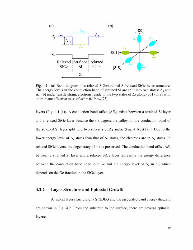
4.2.2 Layer Structure and Epitaxial Growth
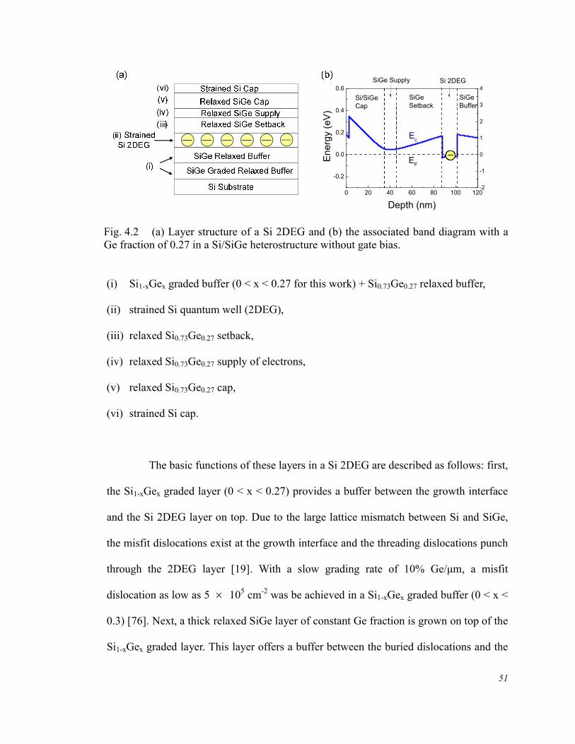
A typical layer structure of a Si 2DEG and the associated band energy diagram
are shown in Fig. 4.2. From the substrate to the surface, there are several epitaxial
layers:
51
0 20 40 60 80 100 120
-0.2
0.0
0.2
0.4
0.6
Energ
y (
eV
)
Depth (nm)
-2
-1
0
1
2
3
4
EF
SiGeBuffer
Si 2DEG
Si/SiGeCap
SiGeSetback
Ec
SiGe Supply
Fig. 4.2 (a) Layer structure of a Si 2DEG and (b) the associated band diagram with a Ge fraction of 0.27 in a Si/SiGe heterostructure without gate bias.
(i) Si1-xGex graded buffer (0 < x < 0.27 for this work) + Si0.73Ge0.27 relaxed buffer,
(ii) strained Si quantum well (2DEG),
(iii) relaxed Si0.73Ge0.27 setback,
(iv) relaxed Si0.73Ge0.27 supply of electrons,
(v) relaxed Si0.73Ge0.27 cap,
(vi) strained Si cap.
The basic functions of these layers in a Si 2DEG are described as follows: first,
the Si1-xGex graded layer (0 < x < 0.27) provides a buffer between the growth interface
and the Si 2DEG layer on top. Due to the large lattice mismatch between Si and SiGe,
the misfit dislocations exist at the growth interface and the threading dislocations punch
through the 2DEG layer [19]. With a slow grading rate of 10% Ge/μm, a misfit
dislocation as low as 5 105 cm-2 was be achieved in a Si1-xGex graded buffer (0 < x <
0.3) [76]. Next, a thick relaxed SiGe layer of constant Ge fraction is grown on top of the
Si1-xGex graded layer. This layer offers a buffer between the buried dislocations and the
52
2DEG layer on top to reduce the electron scattering by those dislocations.
For (ii), a strained Si layer - where the 2DEG resides - is grown between two
relaxed Si0.73Ge0.27 layers, forming a quantum well for electron confinement. The
thickness of this layer is limited by the critical thickness of a strained Si layer on a
relaxed SiGe layer, so as to prevent any further induced dislocations. A relaxed
Si0.73Ge0.27 setback layer (iii) not only provides the required energy confinement for
electrons in the Si QW layer, but also separates the supply layer of ionized impurities
from the 2DEG, leading to less impurity scattering. With the remote supply layer of
n-type doping (iv), electrons can be “supplied” to the Si QW layer. Due to the separation
of 2DEG and those ionized impurities in the supply layer, electron scattering can be
significantly reduced, resulting in very high electron mobility.
Due to the surface segregation of the n-type dopants in the SiGe layers
(chapter 3), a thick SiGe cap layer (v) has to be grown to avoid a high doping level at
the surface which induces high gate leakage current through a Schottky barrier on the
surface. Finally, a Si cap layer offers a much more stable surface than a SiGe layer,
which is crucial for the subsequent processing steps.
In our work, the relaxed SiGe buffer layers were provided by Amberwave Inc.
with a graded Si1-xGex layer (0 < x < 0.27) of a grading rate of 10% Ge/μm grown on top
of Si substrates followed by a Si0.73Ge0.27 buffer layer of 2 μm. Chemical mechanical
polishing (CMP) was applied to reduce the surface roughness prior to the epitaxial
growth. The wafers were cleaned by the following steps: 5 min in diluted HF (1%), 15
min in H2SO4: H2O2 (2.5:1), followed by 2 min in diluted HF (1%). Next, the wafers
were heated to 850 oC for 5 min in hydrogen gas at 6 torr to remove the residual oxide
53
0 50 100 150 200 250 3001015
1016
1017
1018
1019
1020
1021
Impurity
Con
centr
ation (
cm
-3)
Depth (nm)
0
5
10
15
20
25
30
35
B
PC
O
Ge
Fra
ctio
n (
%)
Ge
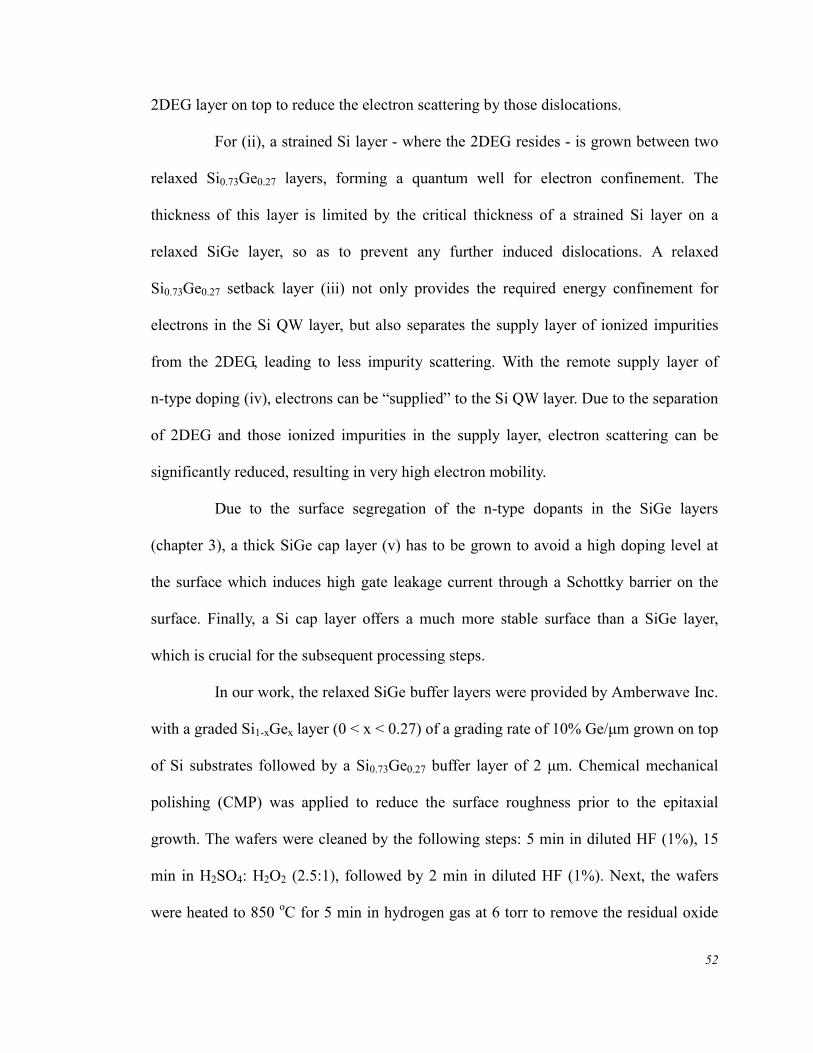
Fig. 4.3 SIMS analysis of a typical Si 2DEG (sample #5737). Ge, P, B, C, and O were measured from the surface to below the growth interface at a depth of 255 nm.
before the epitaxial growth began. The flow rate of hydrogen was 3 slm. Diluted SiH4
(10 % in argone) of 50 sccm and GeH4 (0.8 % in hydrogen) of 76 sccm were used for
the growth of the Si and SiGe epitaxial layers. The growth rates of Si at 625 oC and SiGe
at 575 oC were 0.5 nm/min and 5 nm/min, respectively. Diluted phosphine (100 ppm in
hydrogen) of 2 sccm was used as a doping gas for the growth of an n-type SiGe supply
layer. After baking, a SiGe buffer layer of 100 ~ 150 nm was grown at 575 oC, followed
by a strained-Si layer (2DEG layer) of 6 ~ 30 nm at 625 oC, a SiGe setback layer of 10 ~
70 nm at 575 oC, a n-type SiGe supply layer of 10 nm at 575 oC with a doping level
between 1018 to 1019 cm-3, a SiGe cap layer of 20 ~ 50 nm at 575 oC, and a Si cap layer
of 2 nm at 625 oC.
The layer thicknesses, doping level and Ge fraction were measured by SIMS.
54
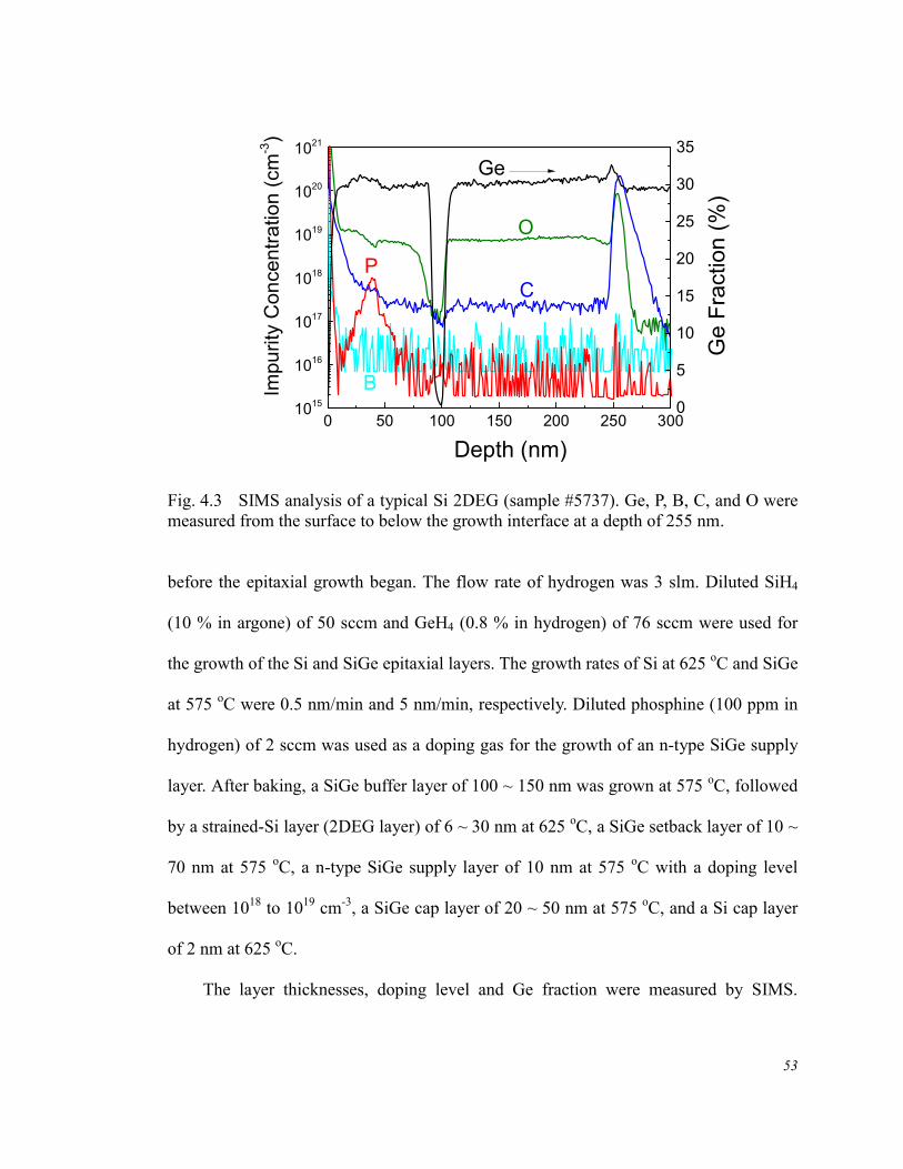
Fig. 4.4 Top view of a typical Hall bar device. Hall bar was first mesa-etched by RIE followed by alloyed AuSb (1 % Sb) for electrical contacts.
Ge, P, B, C, and O in a typical modulation-doped Si 2DEG (sample # 5737) are plotted
versus depth in Fig. 4.3. At a depth of 96 nm, a strained Si QW layer of 12 nm is
sandwiched between the relaxed SiGe layers. The thickness of the SiGe setback layer is
50 nm between the upper SiGe/Si interface and the position of the peak phosphorus
level. The surface segregation of phosphorus was suppressed with a turn-off slope of 13
nm/decade in the SiGe cap layer, which was grown at 525 oC. At the re-growth interface
of depth 255 nm, a spike of C and O indicates the incomplete removal of contaminants.
Although baking at higher temperatures can be used for the better cleaning of the growth
interface, dislocations can be created via the strain relaxation of the underlying graded
Si1-xGex layer. Thus, other approaches such as in-situ cleaning using HCl or HF [77], or
a thick SiGe buffer layer which increases the distance of remote scattering at the growth
interface to 2DEG [78], were suggested. In this work, the latter approach was used and
the experimental results are presented in section 4.4.1. The C levels in the SiGe and Si
layers are 1.8 1017 and 8 1016 cm-3, respectively. The O levels in the SiGe and Si
layers are 7.3 1018, and 1.5 1017 cm-3, respectively.
55
After the growth, the wafers were mesa-etched to the Hall bar geometry,
followed by AuSb deposition (1% Sb) and annealing at 450 oC over 10 minutes for
electrical contacts. For the gating experiment (in section 4.5), palladium was thermally
evaporated in order to cover the entire Hall bar for Schottky gating on single 2DEG
devices. The typical Hall bar device is shown in Fig. 4.4. For low-temperature
measurements, samples were first wire bonded and dipped into a liquid helium dewar at
4 K or 0.3 K. The Hall measurements were performed by lock-in technique to measure
the longitudinal (Rxx) and transverse (Rxy) magneto-resistances for the analysis of
electron density and mobility. The typical drive current is 100 nA.
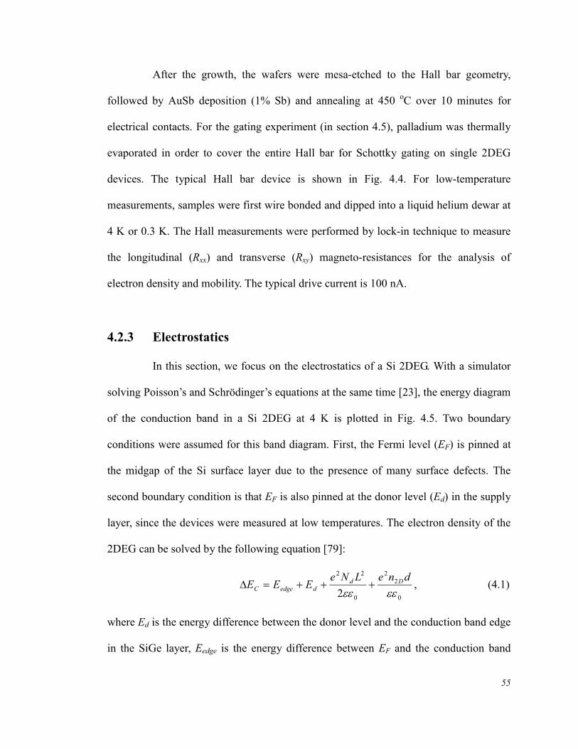
4.2.3 Electrostatics
In this section, we focus on the electrostatics of a Si 2DEG. With a simulator
solving Poisson’s and Schrödinger’s equations at the same time [23], the energy diagram
of the conduction band in a Si 2DEG at 4 K is plotted in Fig. 4.5. Two boundary
conditions were assumed for this band diagram. First, the Fermi level (EF) is pinned at
the midgap of the Si surface layer due to the presence of many surface defects. The
second boundary condition is that EF is also pinned at the donor level (Ed) in the supply
layer, since the devices were measured at low temperatures. The electron density of the
2DEG can be solved by the following equation [79]:
0
22
0
22
2
dneLNeEEE Dd
dedgeC , (4.1)
where Ed is the energy difference between the donor level and the conduction band edge
in the SiGe layer, Eedge is the energy difference between EF and the conduction band
56
0 20 40 60 80 100 120
-0.2
0.0
0.2
0.4
0.6
d
supply setback
Ec
Eedge
L
EF
2DEG0.5 Eg
En
erg
y (
eV
)
Depth (nm)
Ed
IonizedDonor
Fig. 4.5 Conduction band diagram of a Si 2DEG at 4 K with two boundary conditions for the Fermi level (EF) to be pinned at (i) the mid-gap of Si surface and (ii) the donor level.
edge at the upper SiGe/Si interface, and the last two terms represent the energy drop
across the ionized impurity in the charged supply layer of length L and the neutral
setback layer of length d. We assume zero doping in the Si QW and in the structure
below the QW, so the electric field below the quantum well is zero.
Since the typical 2DEG density and the doping level are on the order of 1011
cm-2 and 1018 cm-3, respectively, the required width L can be calculated by Nd L = n2D ~
1 nm, which is much smaller than the thickness of the setback layer (20 ~ 70 nm).
Therefore, the third term in Eq. (4.1) is usually ignored. Furthermore, because Eedge of ~
hundreds μeV is fairly small compared to ΔEc (~ 180 meV for Si0.7Ge0.3 [80]), to first
order only, the second and last terms are considered in the analysis. The electron density
n2D in the Si QW layer can be solved as:
57
d
EE
en dC
D
2
02
. (4.2)
This shows that the density at equilibrium (without external gating) can be manipulated
by adjusting the conduction band offset (i.e., changing the Ge fraction in the SiGe
barrier) or the thickness of the setback SiGe layer. In this work, the Ge fraction is fixed
at 0.27 and we focus on the effect of the SiGe setback layer thickness on 2DEG
characteristics (section 4.4.3).
4.2.4 Mobility Model
To investigate the scattering mechanisms in a Si 2DEG, we followed the
procedures derived by Davies [79]. For quantum dot applications, achieving a single
electron would require a low density in a 2DEG or a small dot area by a simple relation
of 1 = n2D Area. With a QD of 30 nm 30 nm (typical of advanced lithography),
n2D must be at most ~ 1 1011 cm-2. Thus, we focus on the transport properties of the
2DEGs at densities below 4 1011 cm-2, where remote or background impurity
scattering has been suggested as the dominant scattering mechanism [81, 82].
The strongest scattering at low temperatures in many 2DEG systems arises
from ionized impurities such as n-type donors in the supply layer or throughout the
entire material. The former is usually called ‘remote impurity scattering’ and the latter is
usually referred to as ‘background impurity scattering’ [79, 82]. For remote impurity
scattering, we assumed for simplicity that the supply layer is delta-doped with a
two-dimensional density of Nimp ionized impurity, and located at a distance of d from the
doping plane to the edge of the Si QW layer. The resulting electron transport time based
58
on Fermi-Golden’s rule can be expressed as [79]
32
3* 32
1
D
imp
tr ndm
N
, (4.3)
where m* is the effective mass of electron in the Si QW layer and the effects of the
degeneracy of the two valley states and two spin states were already included. Next, the
mobility (m
e tr ) is given by
imp
D
remoteN
ned
32
3 32 . (4.4)
When n2D increases, there is stronger electron screening [79] and so the mobility
increases. As the distance between the plane of ionized impurities and the 2DEG
increases, electron scattering is weaker and the mobility is higher. On the other hand, as
the number of ionized impurities is reduced, the remote scattering becomes weaker and
the mobility increases.
Ideally, in a 2DEG structure, the only doped region is the supply layer.
However, in practice - in other layers a minimum level of certain types of impurities
exists, depending upon the reactor history and growth conditions. The ionized
background impurities across the entire sample also scatter the 2DEG with a predicted
mobility as:
background
Dbackground
N
ne
22
. (4.5)
In a similar manner to remote impurity scattering, as the electron density increases, the
background impurity scattering is reduced due to stronger electron screening. When the
59
number of ionized background impurities is reduced, the scattering will be weaker.
The total mobility related to these two types of impurities can be written as:
backgroundremotetotal
111 . (4.6)
In the next section, we will show the importance of background scattering in a Si 2DEG
that has been grown. Afterwards, we present a much improved mobility by reducing the
background impurity level in the CVD system at Princeton University.
The above model of 2DEG mobility was proposed with several assumptions,
such as the delta doping in the supply layer. In practice, broadened n-type doping
profiles in the SiGe layer are caused by strong surface segregation (chapter 3), which
might offset the predicted mobility by the above model. Furthermore, the abruptness of
the SiGe/Si/SiGe heterostructure may not be perfectly sharp, resulting in a perturbation
on the quantum states in the Si QW layer. During the derivation for electron screening,
many numerical approximations were made [79]. This made the derivation easier, but is
not of spectacular accuracy. As a result, in this work, we use this theoretical model only
as a rough guide to help us to understand the electron transport properties, but not for
any precise numerical fitting or model comparison with our data.
4.3 Efforts Toward High Mobility in Si 2DEGs
4.3.1 Effects of Phosphorus Background Impurity on 2DEG Mobility
In CVD systems, the background level of n-type dopants such as phosphorus
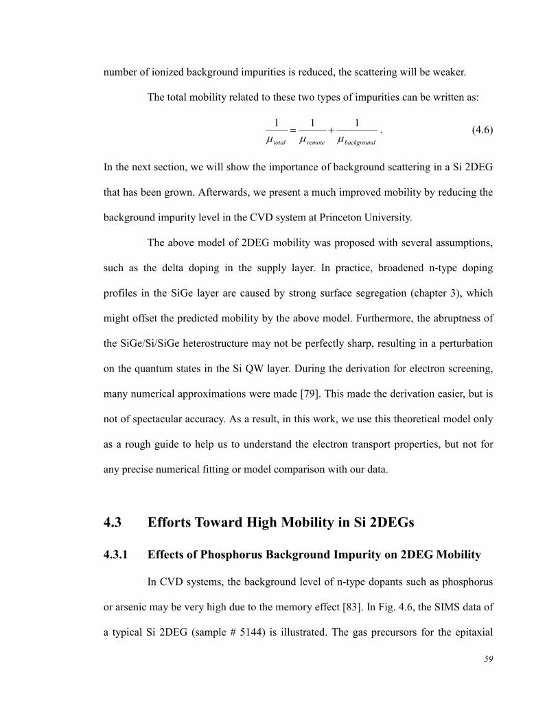
or arsenic may be very high due to the memory effect [83]. In Fig. 4.6, the SIMS data of
a typical Si 2DEG (sample # 5144) is illustrated. The gas precursors for the epitaxial
60
0 50 100 150 200 250 3001014
1015
1016
1017
1018
1019
1020
B
P
Impurity
Concentr
ation (
cm
-3)
Depth (nm)
Ge
0
5
10
15
20
25
30
35
40
Ge F
raction (
%)
Fig. 4.6 SIMS results of a Si 2DEG (sample #5144). The phosphorus background levels in the Si and SiGe layers are 6 1017 cm-3 and 2 1017 cm-3, respectively.
growth of this sample were SiH2Cl2 and diluted GeH4 with diluted PH3 as the n-type
doping gas. At a depth of 40 nm, a phosphorus doped layer of 1.5 1018 cm-3 was
grown. The phosphorus background levels in the Si and SiGe layers are 6 1017 cm-3
and 2 1017 cm-3, respectively. Note that below the growth interface at 250 nm, the
phosphorus level in the relaxed buffer grown by Amberwave Inc. is below 1015 cm-3,
showing that the phosphorus levels in the epitaxial layers grown by our CVD are true
and not artifacts or detection limits from the SIMS measurements. By assuming n2D ~ 5
1011 cm-2 and ignoring the remote impurity scattering, the electron mobility at a
background impurity of 5 1017 cm-3 can be estimated by Eq. (4.5) as 5,000 cm2/V-s,
which is close to our experimental results of 3,000 ~ 8,000 cm2/V-s. Thus, the first task
in improving the 2DEG mobility is to lower the background impurity level in the
epitaxial layers.
61
4.3.2 The Reduction of Phosphorus Background Impurity Levels
A low phosphorus background level has been suggested for a 2DEG of high
mobility. In this section, we will introduce the means by which we identified the sources
for high background level of phosphorus in our CVD system, followed by an approach
to reduce the phosphorus level and our experimental results.
First, we evaluate the impact of the potential sources for a high phosphorus
level, such as the quartz tube and the quartz wafer holder. Since the Si wafers were often
baked or annealed at high temperatures (~ 1000 oC) in our CVD system, phosphorus
adsorbed on the quartz walls might desorb and incorporate into the epitaxial films. To
remove the coated phosphorus on the quartz wall and the wafer stand, we used
HF:HNO3:H2O (1:4: 6) to etch the deposited films on the quartz surface, followed by a
DI water rinse. However, in a test 2DEG structure grown after the wet cleaning steps,
the phosphorus background level was rather high (~ 1017 cm-3) and the mobility was still
low (5,000 ~ 10,000 cm2/V-s). Even with a brand new tube and wafer stand used for the
growth of 2DEG devices, identical results of the high background level of phosphorus
and low mobility were obtained. This suggests that the main source of phosphorus
contamination was not the tubes or wafer stands.
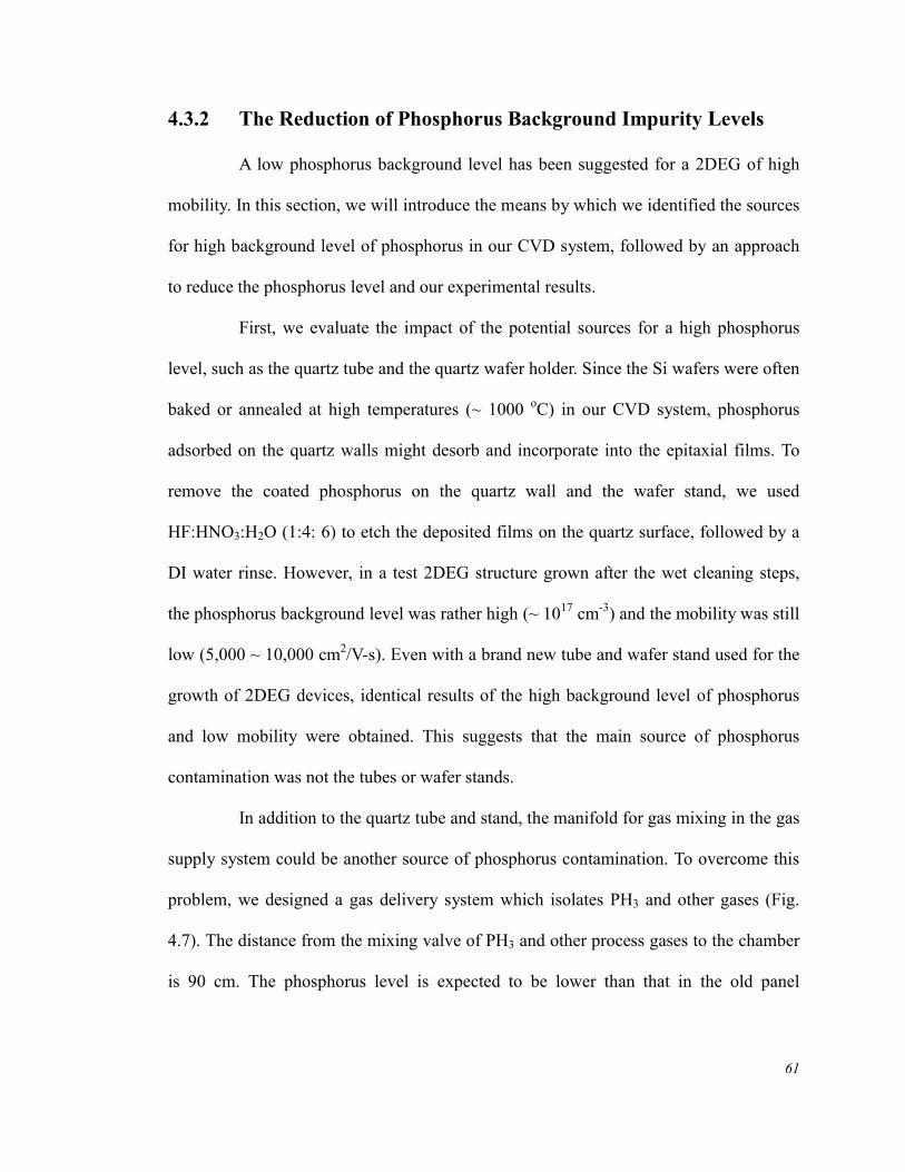
In addition to the quartz tube and stand, the manifold for gas mixing in the gas
supply system could be another source of phosphorus contamination. To overcome this
problem, we designed a gas delivery system which isolates PH3 and other gases (Fig.
4.7). The distance from the mixing valve of PH3 and other process gases to the chamber
is 90 cm. The phosphorus level is expected to be lower than that in the old panel
62
Fig. 4.7 New gas supply system with separation of process gases (H2, SiH4, GeH4, etc.) from PH3 to reduce the memory effect of phosphorus.
0 100 200 300 400 5001014
1015
1016
1017
1018
1019
1020
B
P
Impurity
Concentr
ation (
cm
-3)
Depth (nm)
Ge
0
5
10
15
20
25
30
35
40
Ge
Fra
ctio
n (
%)
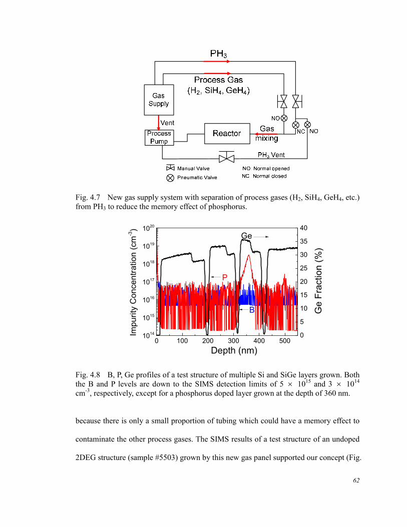
Fig. 4.8 B, P, Ge profiles of a test structure of multiple Si and SiGe layers grown. Both the B and P levels are down to the SIMS detection limits of 5 1015 and 3 1014 cm-3, respectively, except for a phosphorus doped layer grown at the depth of 360 nm.
because there is only a small proportion of tubing which could have a memory effect to
contaminate the other process gases. The SIMS results of a test structure of an undoped
2DEG structure (sample #5503) grown by this new gas panel supported our concept (Fig.
63
0 50 100 150 200 250 300 3501014
1015
1016
1017
1018
750 oC625 oC575 oC
P
Imp
urity
Co
nce
ntr
atio
n (
cm
-3)
Depth (nm)
700 oC
B
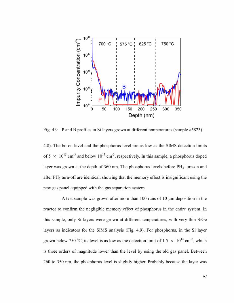
Fig. 4.9 P and B profiles in Si layers grown at different temperatures (sample #5823).
4.8). The boron level and the phosphorus level are as low as the SIMS detection limits
of 5 1015 cm-3 and below 1015 cm-3, respectively. In this sample, a phosphorus doped
layer was grown at the depth of 360 nm. The phosphorus levels before PH3 turn-on and
after PH3 turn-off are identical, showing that the memory effect is insignificant using the
new gas panel equipped with the gas separation system.
A test sample was grown after more than 100 runs of 10 μm deposition in the
reactor to confirm the negligible memory effect of phosphorus in the entire system. In
this sample, only Si layers were grown at different temperatures, with very thin SiGe
layers as indicators for the SIMS analysis (Fig. 4.9). For phosphorus, in the Si layer
grown below 750 oC, its level is as low as the detection limit of 1.5 1014 cm-2, which
is three orders of magnitude lower than the level by using the old gas panel. Between
260 to 350 nm, the phosphorus level is slightly higher. Probably because the layer was
64
grown immediately after high temperature baking, the desorption of the absorbed
phosphorus on the quartz wall was stronger, leading to higher incorporation into the
films. For boron, although it is as low as 3 1014 cm-3, it is surprising that its level is
slightly higher, since a boron precursor has never been used in the new gas panel. The
low boron level in the system could be a SIMS effect or the auto-doping from the lightly
boron-doped SiGe relaxed buffer substrates grown by Amberwave Inc.
4.3.3 Transport Properties of Si 2DEGs with Low Phosphorus
Background Impurity Levels
To estimate the effect of a low background level of mid 1014 cm-3 on 2DEG
mobility, we assumed that the 2DEG mobility is limited by the background impurity
scattering. Using Eq. (4.5), we estimated a mobility of 3 106 cm2/V-s, which is
almost 10 times higher than the highest mobility reported in this work. Therefore, it is
suggested that the mobility in 2DEGs grown by this new gas system is not limited by
background impurity scattering, but rather that it is limited by remote impurity
scattering. Further experimental results in the following sections confirm our
conclusions.
Si 2DEGs of low background impurity were epitaxially grown with the new
gas panel and fabricated into Hall bar devices. The low-temperature (4 K and 0.3 K)
electron density and mobility of Si 2DEGs with different layer structures (i.e. varying
the SiGe setback layer thickness, the doping level, SiGe cap layer thickness, etc.) were
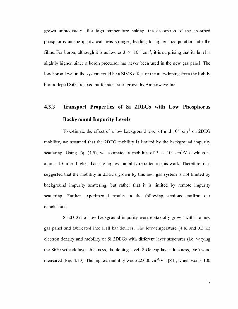
measured (Fig. 4.10). The highest mobility was 522,000 cm2/V-s [84], which was ~ 100
65
1011
1012
105
106
4 K
H
all (c
m2/V
-s)
nHall
(cm-2)
0.3 K
Fig. 4.10 Hall mobility vs. electron density at low temperatures (4 K or 0.3 K). A highest mobility of 522,000 cm2/V-s was measured at 0.3 K [84]. Note that each data point was taken from different samples with different layer structures.
0 1 2 3 4 5 6 7 80.00
0.05
0.10
Rxx
k
/
)
B (tesla)
T ~ 0.3K
0.0
0.1
0.2
Rxy h
(h/e
2)
1110 9 57 6162024 8Filling factor12
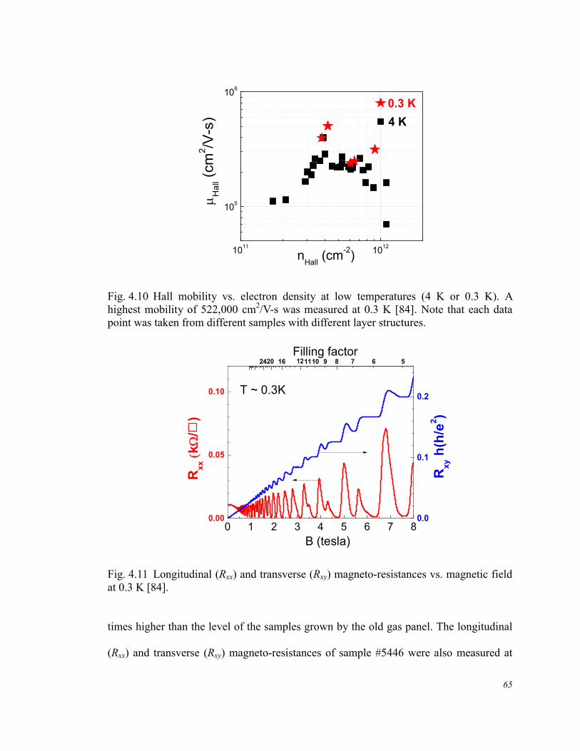
Fig. 4.11 Longitudinal (Rxx) and transverse (Rxy) magneto-resistances vs. magnetic field at 0.3 K [84].
times higher than the level of the samples grown by the old gas panel. The longitudinal
(Rxx) and transverse (Rxy) magneto-resistances of sample #5446 were also measured at
66
0.3 K by Prof. Rokhinson at Purdue University (Fig. 4.11). Clear Shubnikov-de Haas
oscillations in Rxx and quantum Hall plateaus in Rxy were observed, showing the high
quality of this sample. The spin splitting and valley splitting occurred at 0.8 T and 3.5 T,
respectively. Overshoots of Rxy at odd filling factors were observed. Several suggestions
have been made to explain such effects, such as a rapid decoupling of overlapping
spin-split states [85] and a mixing of overlapping edge states and the intrinsic spin-orbit
interaction of 2DEGs [86]. These effects are beyond the scope of this thesis.
4.4 Effects of Layer Structure on 2DEG Mobility
4.4.1 SiGe Buffer Layer
Typically, a Si 2DEG structure is epitaxially grown on a Si (100) substrate,
either by MBE or CVD. In Princeton, we grew the epitaxial layers of a Si 2DEG on a
virtual substrate which consisted of a relaxed SiGe buffer layer on top of a graded SiGe
layer on a Si substrate (provided by Amberwave Inc.). Prior to the growth, chemical
mechanical polish was applied to reduce the surface roughness, followed by a wet
cleaning to remove the residual contaminants and native oxide on the polished relaxed
SiGe surface. Next, SiGe and Si epitaxial layers were grown using the new gas supply
system, and Hall bar devices were fabricated for electron transport measurement at low
temperatures.
As depicted in Fig. 4.3, there were spikes of C and O at the substrate interface
due to inefficient cleaning before epitaxy. Paul et al. have suggested that with a thick
SiGe buffer layer on the SiGe virtual substrate, electron scattering from the bottom
67
growth interface was much reduced [78]. Therefore, we grew test samples (#5858,
#5838, and #5862) with three different thicknesses of the SiGe buffer layer (50, 155, and
310 nm), while the rest of the layer structures in those three samples were identical to
each other (Table 4.1).
Table 4.1 Layer structures of sample #5858, #5838, and #5862 for study of the effects of SiGe buffer layer thickness on the 2DEG mobility
Thickness (nm)
Sample #
Growth Temp
(oC) 5858 5838 5862
Si cap 625 4 4 4
SiGe cap 550 50 ~ 70 50 ~ 70 50 ~ 70
SiGe supply 575 10 10 10
P level (cm-3) 575 1 ~ 4 1018 1 ~ 4 1018 1 ~ 4 1018
SiGe setback 575 30 30 30
Si QW 625 10 10 10
SiGe buffer 575 50 155 310
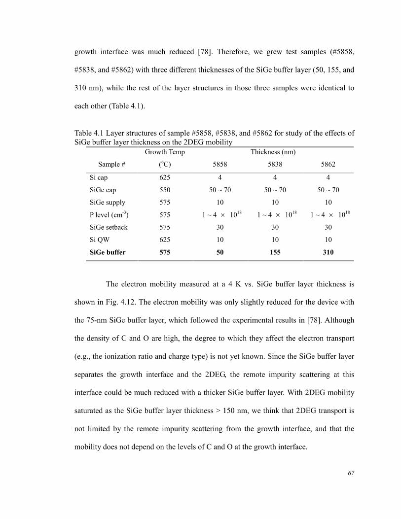
The electron mobility measured at a 4 K vs. SiGe buffer layer thickness is
shown in Fig. 4.12. The electron mobility was only slightly reduced for the device with
the 75-nm SiGe buffer layer, which followed the experimental results in [78]. Although
the density of C and O are high, the degree to which they affect the electron transport
(e.g., the ionization ratio and charge type) is not yet known. Since the SiGe buffer layer
separates the growth interface and the 2DEG, the remote impurity scattering at this
interface could be much reduced with a thicker SiGe buffer layer. With 2DEG mobility
saturated as the SiGe buffer layer thickness > 150 nm, we think that 2DEG transport is
not limited by the remote impurity scattering from the growth interface, and that the
mobility does not depend on the levels of C and O at the growth interface.
68
0 100 200 300104
105
106
Mobili
ty (
cm
2/V
-s)
SiGe Buffer Thickness (nm)
Fig. 4.12 Electron Mobility at 4 K vs. SiGe buffer layer thickness.
4.4.2 Si Quantum Well Layer
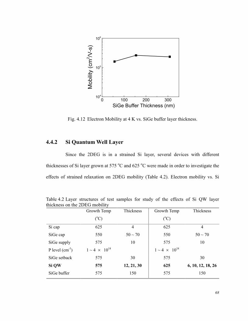
Since the 2DEG is in a strained Si layer, several devices with different
thicknesses of Si layer grown at 575 oC and 625 oC were made in order to investigate the
effects of strained relaxation on 2DEG mobility (Table 4.2). Electron mobility vs. Si
Table 4.2 Layer structures of test samples for study of the effects of Si QW layer thickness on the 2DEG mobility
Growth Temp
(oC)
Thickness Growth Temp
(oC)
Thickness
Si cap 625 4 625 4
SiGe cap 550 50 ~ 70 550 50 ~ 70
SiGe supply 575 10 575 10
P level (cm-3) 1 ~ 4 1018 1 ~ 4 1018
SiGe setback 575 30 575 30
Si QW 575 12, 21, 30 625 6, 10, 12, 18, 26
SiGe buffer 575 150 575 150
69
0 10 20 30103
104
105
106
575oC
Mo
bili
ty (
cm
2/V
-s)
Si QW Thickness (nm)
625oC
Fig. 4.13 Mobility at a 4 K vs. Si QW layer thickness grown at 575 oC and 625 oC. The arrow indicates the predicted critical thickness of strained Si on the relaxed Si0.73Ge0.27 [87].
QW thickness is shown in Fig. 4.13. A peak near 10 nm is observed. For the 625 oC data,
the Si QW is thicker than 12 nm, and the mobility drops significantly as the thickness
increases. This may due to dislocations created by the strain relaxation of the thick Si
QW layer. The thickness at which mobility drops significantly is close to the reported
critical thickness (~ 12 nm) of a strained Si layer on a relaxed Si0.73Ge0.27 layer [87]. For
575 oC, a similar trend was observed.
On the other hand, when the Si QW is under 10 nm (e.g. 6 nm), the 2DEG
mobility drops slightly when the well is thinner, which could be attributed to the
stronger scattering from the roughness at the upper SiGe/Si heterointerface [88]. In a
narrow QW, the spreading of electron wavefunction into the SiGe barrier layers
becomes stronger, which might also lead to stronger scattering from the remote impurity
in the supply layer or alloy scattering in the SiGe barrier [82]. Thus, when we discuss
70
the ionized impurity scattering in the next section, the thickness of the strained Si QW
layer is controlled between 9 to 12 nm and to more easily isolate the effects of different
scattering mechanisms on 2DEG mobility.
4.4.3 SiGe Setback Layer
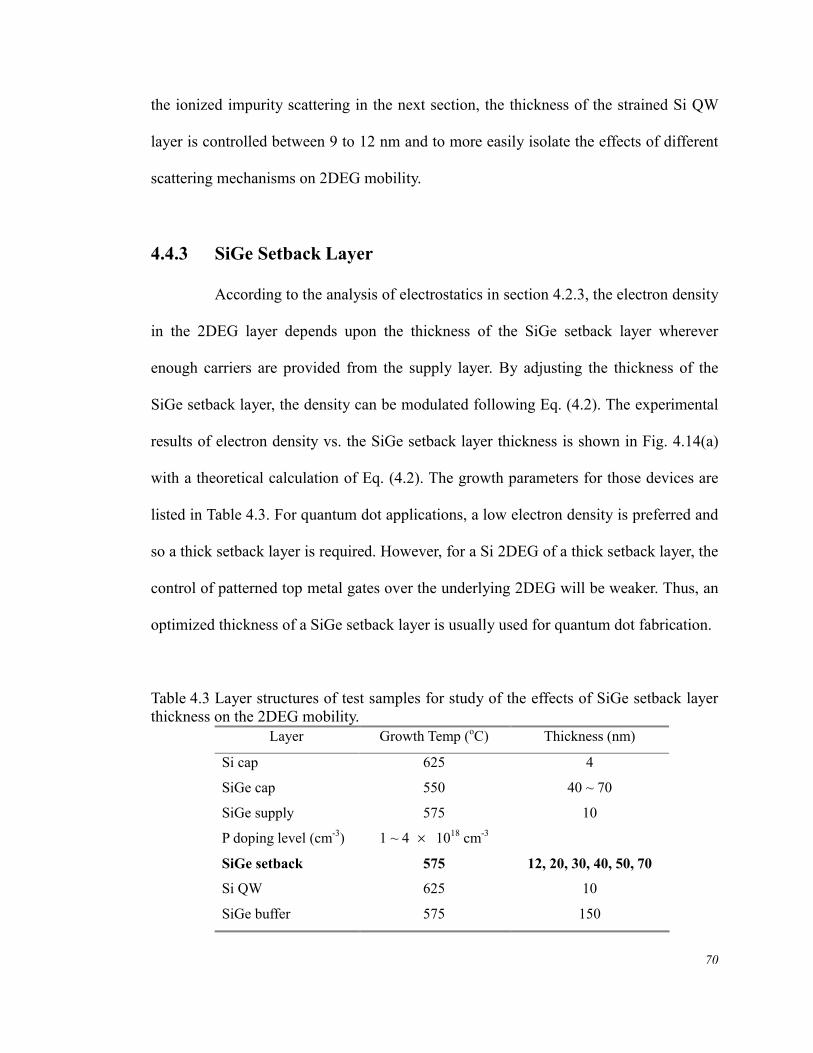
According to the analysis of electrostatics in section 4.2.3, the electron density
in the 2DEG layer depends upon the thickness of the SiGe setback layer wherever
enough carriers are provided from the supply layer. By adjusting the thickness of the
SiGe setback layer, the density can be modulated following Eq. (4.2). The experimental
results of electron density vs. the SiGe setback layer thickness is shown in Fig. 4.14(a)
with a theoretical calculation of Eq. (4.2). The growth parameters for those devices are
listed in Table 4.3. For quantum dot applications, a low electron density is preferred and
so a thick setback layer is required. However, for a Si 2DEG of a thick setback layer, the
control of patterned top metal gates over the underlying 2DEG will be weaker. Thus, an
optimized thickness of a SiGe setback layer is usually used for quantum dot fabrication.
Table 4.3 Layer structures of test samples for study of the effects of SiGe setback layer thickness on the 2DEG mobility.
Layer Growth Temp (oC) Thickness (nm)
Si cap 625 4
SiGe cap 550 40 ~ 70
SiGe supply
P doping level (cm-3)
575
1 ~ 4 1018 cm-3
10
SiGe setback 575 12, 20, 30, 40, 50, 70
Si QW 625 10
SiGe buffer 575 150
71
10 20 30 40 50 60 700
1x10⁵
2x10⁵
3x10⁵
4x10⁵
(
cm
2/V
-S)
SiGe Setback Layer (nm)
10 20 30 40 50 60 70
2.0x10¹¹
4.0x10¹¹
6.0x10¹¹
8.0x10¹¹
1.0x10¹²
Theoryn (
cm
-2)
SiGe Setback Layer (nm)
Experiment
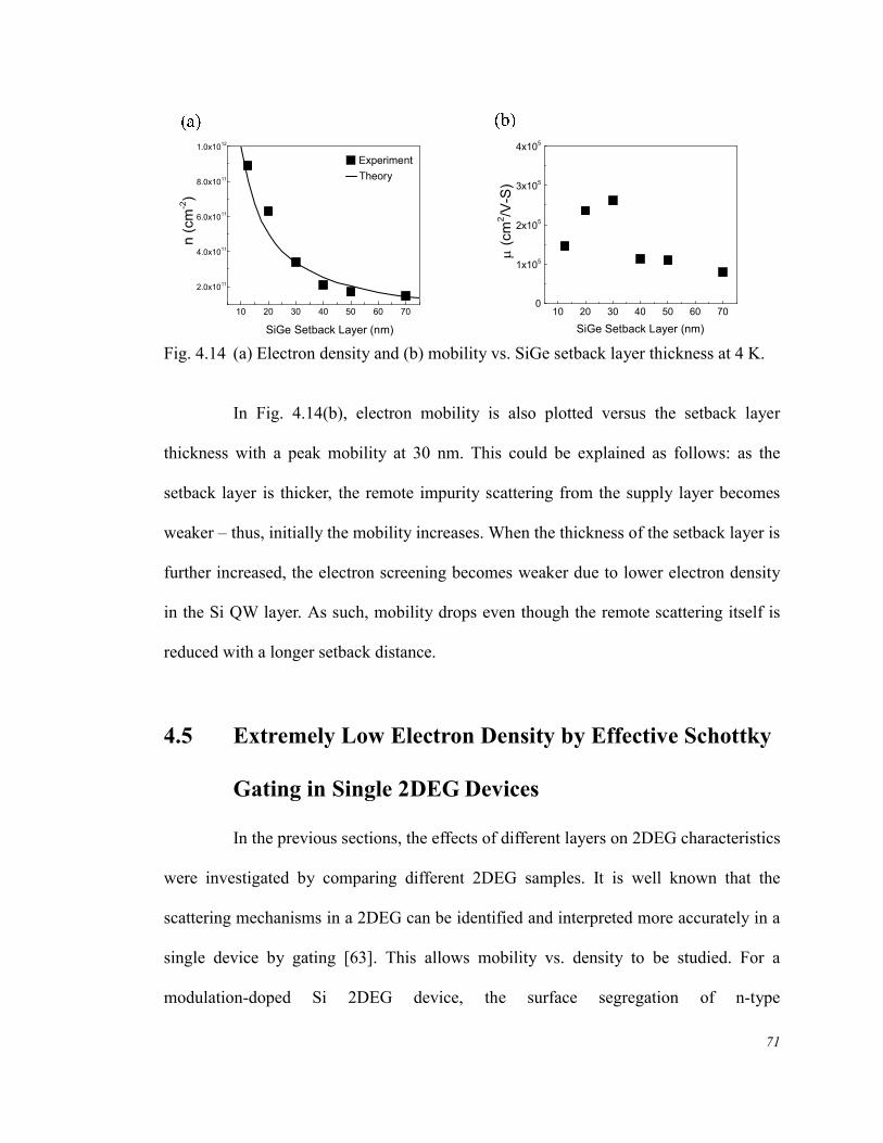
Fig. 4.14 (a) Electron density and (b) mobility vs. SiGe setback layer thickness at 4 K.
In Fig. 4.14(b), electron mobility is also plotted versus the setback layer
thickness with a peak mobility at 30 nm. This could be explained as follows: as the
setback layer is thicker, the remote impurity scattering from the supply layer becomes
weaker – thus, initially the mobility increases. When the thickness of the setback layer is
further increased, the electron screening becomes weaker due to lower electron density
in the Si QW layer. As such, mobility drops even though the remote scattering itself is
reduced with a longer setback distance.
4.5 Extremely Low Electron Density by Effective Schottky
Gating in Single 2DEG Devices
In the previous sections, the effects of different layers on 2DEG characteristics
were investigated by comparing different 2DEG samples. It is well known that the
scattering mechanisms in a 2DEG can be identified and interpreted more accurately in a
single device by gating [63]. This allows mobility vs. density to be studied. For a
modulation-doped Si 2DEG device, the surface segregation of n-type
72
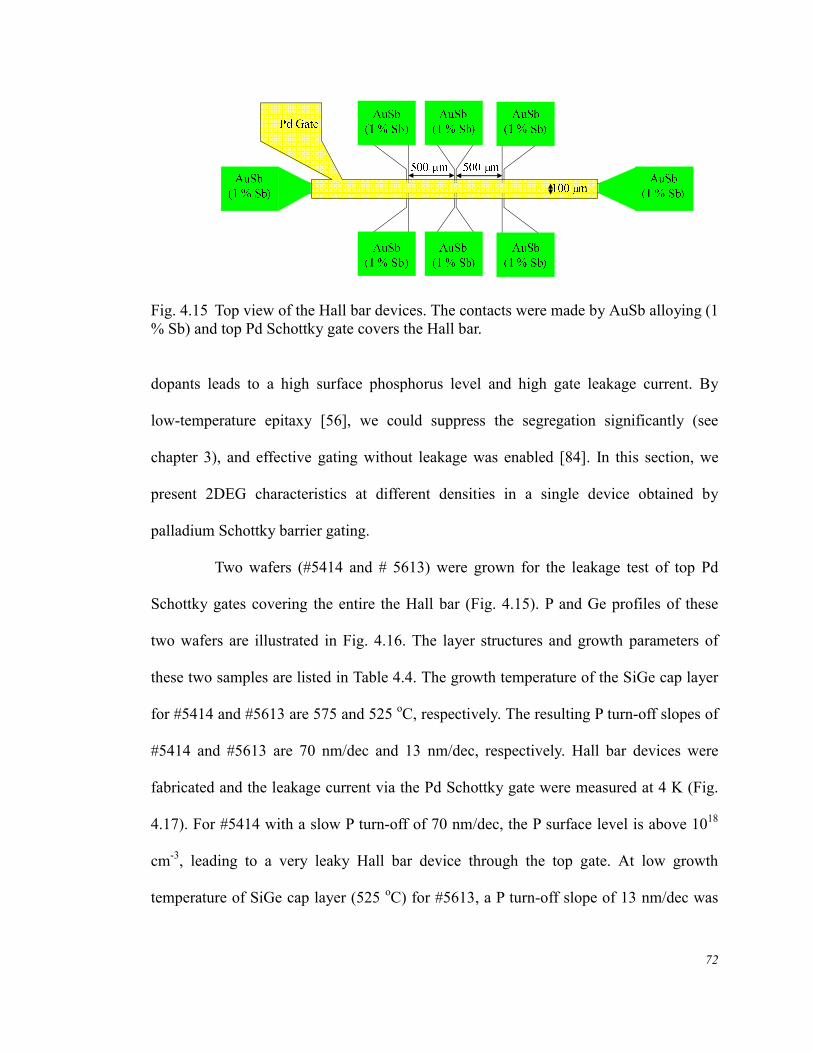
Fig. 4.15 Top view of the Hall bar devices. The contacts were made by AuSb alloying (1 % Sb) and top Pd Schottky gate covers the Hall bar.
dopants leads to a high surface phosphorus level and high gate leakage current. By
low-temperature epitaxy [56], we could suppress the segregation significantly (see
chapter 3), and effective gating without leakage was enabled [84]. In this section, we
present 2DEG characteristics at different densities in a single device obtained by
palladium Schottky barrier gating.
Two wafers (#5414 and # 5613) were grown for the leakage test of top Pd
Schottky gates covering the entire the Hall bar (Fig. 4.15). P and Ge profiles of these
two wafers are illustrated in Fig. 4.16. The layer structures and growth parameters of
these two samples are listed in Table 4.4. The growth temperature of the SiGe cap layer
for #5414 and #5613 are 575 and 525 oC, respectively. The resulting P turn-off slopes of
#5414 and #5613 are 70 nm/dec and 13 nm/dec, respectively. Hall bar devices were
fabricated and the leakage current via the Pd Schottky gate were measured at 4 K (Fig.
4.17). For #5414 with a slow P turn-off of 70 nm/dec, the P surface level is above 1018
cm-3, leading to a very leaky Hall bar device through the top gate. At low growth
temperature of SiGe cap layer (525 oC) for #5613, a P turn-off slope of 13 nm/dec was
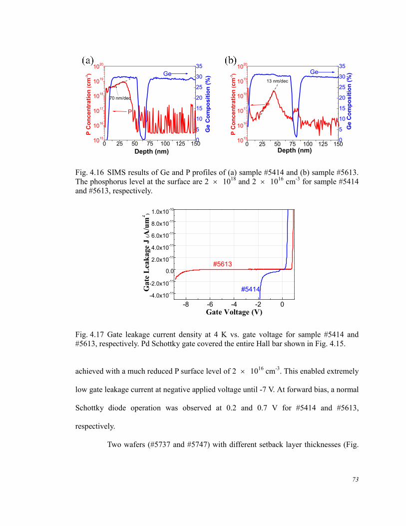
73
0 25 50 75 100 125 15010
15
1016
1017
1018
1019
1020
P C
on
cen
trati
on
(cm
-3)
Depth (nm)
Ge
P
70 nm/dec
0
5
10
15
20
25
30
35
Ge
Co
mp
os
itio
n (
%)
0 25 50 75 100 125 15010
15
1016
1017
1018
1019
1020
13 nm/dec
Ge
P C
on
cen
trati
on
(cm
-3)
Depth (nm)
P
0
5
10
15
20
25
30
35
Ge
Co
mp
os
itio
n (
%)
Fig. 4.16 SIMS results of Ge and P profiles of (a) sample #5414 and (b) sample #5613. The phosphorus level at the surface are 2 1018 and 2 1016 cm-3 for sample #5414 and #5613, respectively.
-8 -6 -4 -2 0
-4.0x10⁻¹¹
-2.0x10⁻¹¹
0.0
2.0x10⁻¹¹
4.0x10⁻¹¹
6.0x10⁻¹¹
8.0x10⁻¹¹
1.0x10⁻¹⁰
#5613
Gate
Lea
kage
J (A
/um
2 )
Gate Voltage (V)
#5414
Fig. 4.17 Gate leakage current density at 4 K vs. gate voltage for sample #5414 and #5613, respectively. Pd Schottky gate covered the entire Hall bar shown in Fig. 4.15.
achieved with a much reduced P surface level of 2 1016 cm-3. This enabled extremely
low gate leakage current at negative applied voltage until -7 V. At forward bias, a normal
Schottky diode operation was observed at 0.2 and 0.7 V for #5414 and #5613,
respectively.
Two wafers (#5737 and #5747) with different setback layer thicknesses (Fig.
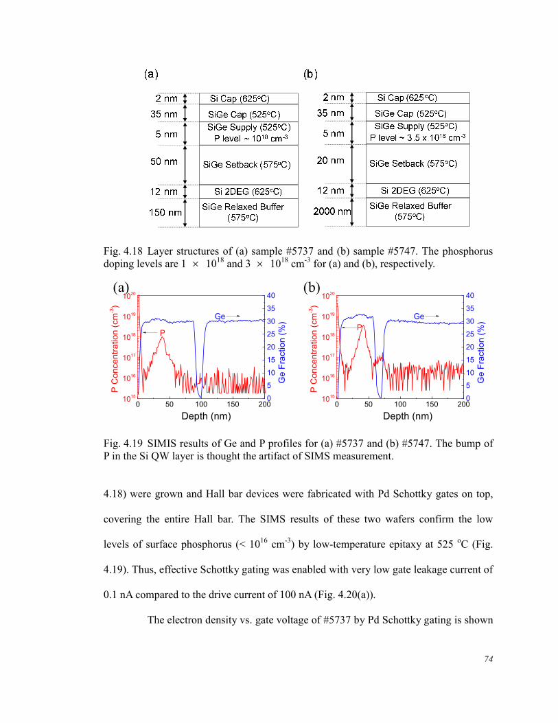
74
Fig. 4.18 Layer structures of (a) sample #5737 and (b) sample #5747. The phosphorus doping levels are 1 1018 and 3 1018 cm-3 for (a) and (b), respectively.
0 50 100 150 2001015
1016
1017
1018
1019
1020
Ge
P C
oncentr
ation (
cm
-3)
Depth (nm)
P
0
5
10
15
20
25
30
35
40
Ge F
raction (
%)
(a) (b)
0 50 100 150 2001015
1016
1017
1018
1019
1020
GeP
Concentr
ation (
cm
-3)
Depth (nm)
P
0
5
10
15
20
25
30
35
40
Ge F
raction (
%)
Fig. 4.19 SIMIS results of Ge and P profiles for (a) #5737 and (b) #5747. The bump of P in the Si QW layer is thought the artifact of SIMS measurement.
4.18) were grown and Hall bar devices were fabricated with Pd Schottky gates on top,
covering the entire Hall bar. The SIMS results of these two wafers confirm the low
levels of surface phosphorus (< 1016 cm-3) by low-temperature epitaxy at 525 oC (Fig.
4.19). Thus, effective Schottky gating was enabled with very low gate leakage current of
0.1 nA compared to the drive current of 100 nA (Fig. 4.20(a)).
The electron density vs. gate voltage of #5737 by Pd Schottky gating is shown
75
-2.0 -1.5 -1.0 -0.5 0.0 0.5 1.010
-12
10-11
10-10
10-9
10-8
10-7
10-6
I g (
A)
Vg (V)
drive current (100nA)
0.0 0.2 0.4 0.60
1
2
3
4
5
6
at 4K
x 1011
nH
all
(cm
-2)
Vg (V)
Cexp
~ 1.2 x 10⁻⁷ F/cm
2
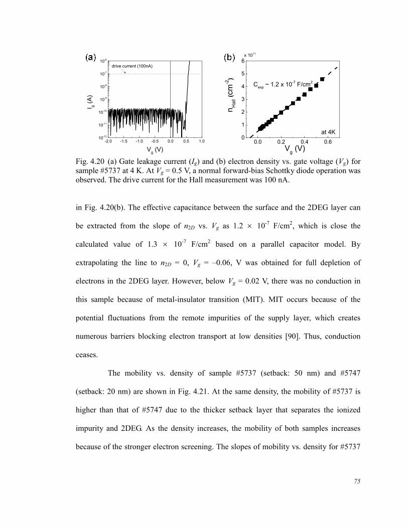
Fig. 4.20 (a) Gate leakage current (Ig) and (b) electron density vs. gate voltage (Vg) for sample #5737 at 4 K. At Vg = 0.5 V, a normal forward-bias Schottky diode operation was observed. The drive current for the Hall measurement was 100 nA.
in Fig. 4.20(b). The effective capacitance between the surface and the 2DEG layer can
be extracted from the slope of n2D vs. Vg as 1.2 10-7 F/cm2, which is close the
calculated value of 1.3 10-7 F/cm2 based on a parallel capacitor model. By
extrapolating the line to n2D = 0, Vg = –0.06, V was obtained for full depletion of
electrons in the 2DEG layer. However, below Vg = 0.02 V, there was no conduction in
this sample because of metal-insulator transition (MIT). MIT occurs because of the
potential fluctuations from the remote impurities of the supply layer, which creates
numerous barriers blocking electron transport at low densities [90]. Thus, conduction
ceases.
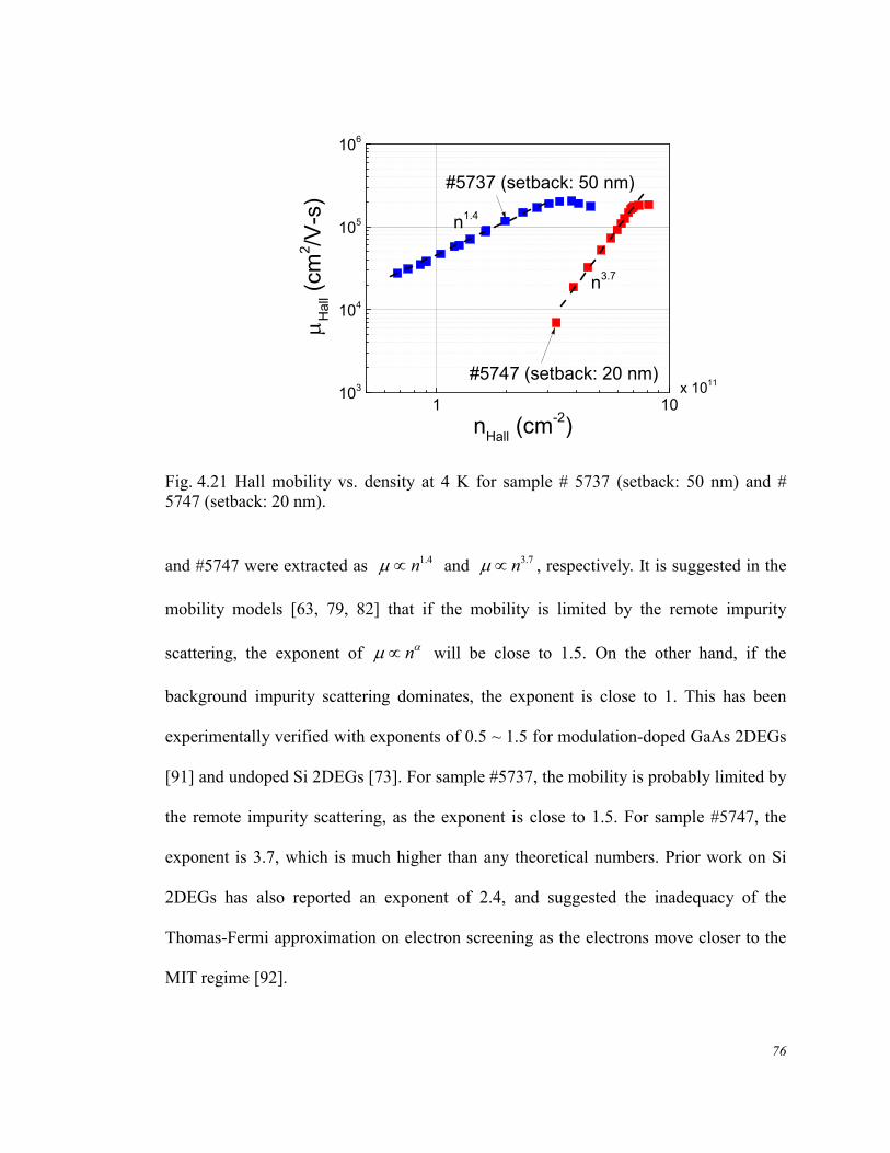
The mobility vs. density of sample #5737 (setback: 50 nm) and #5747
(setback: 20 nm) are shown in Fig. 4.21. At the same density, the mobility of #5737 is
higher than that of #5747 due to the thicker setback layer that separates the ionized
impurity and 2DEG. As the density increases, the mobility of both samples increases
because of the stronger electron screening. The slopes of mobility vs. density for #5737
76
1 10103
104
105
106
n1.4
#5747 (setback: 20 nm)
H
all (c
m2/V
-s)
nHall
(cm-2)
x 1011
#5737 (setback: 50 nm)
n3.7
Fig. 4.21 Hall mobility vs. density at 4 K for sample # 5737 (setback: 50 nm) and # 5747 (setback: 20 nm).
and #5747 were extracted as 4.1n and 7.3n , respectively. It is suggested in the
mobility models [63, 79, 82] that if the mobility is limited by the remote impurity
scattering, the exponent of n will be close to 1.5. On the other hand, if the
background impurity scattering dominates, the exponent is close to 1. This has been
experimentally verified with exponents of 0.5 ~ 1.5 for modulation-doped GaAs 2DEGs
[91] and undoped Si 2DEGs [73]. For sample #5737, the mobility is probably limited by
the remote impurity scattering, as the exponent is close to 1.5. For sample #5747, the
exponent is 3.7, which is much higher than any theoretical numbers. Prior work on Si
2DEGs has also reported an exponent of 2.4, and suggested the inadequacy of the
Thomas-Fermi approximation on electron screening as the electrons move closer to the
MIT regime [92].
77
Note that the MIT occurs at 6.5 1010 and 3.2 1011 cm-2, with mobilities
of 30,000 and 7,000 cm2/V-s for #5737 and #5747, respectively. For sample #5737, the
mobility at n2D = 1 1011 cm-2 is 45,000 cm2/V-s. To our knowledge, this is the highest
mobility reported for modulated-doped Si 2DEGs at a density of 1011 cm-2 - an
indication of the high quality of our 2DEG samples. The higher critical density for MIT
to occur in #5747 is attributed to its shorter setback layer, leading to stronger effects of
potential fluctuations on 2DEG so that the metallic conduction ceases at a higher
electron density [89].
There is a saturation in mobility at n2D = 3.6 1011 and 7.9 1011 cm-2 for
#5737 and #5747. Several reasons could be attributed to the maximum mobility, such as
parallel conduction in the supply layer [93, 94], or the second subband occupancy in the
Si QW layer [95], or the interface roughness scattering [88] at the upper SiGe/Si
interface coming from a higher electric field pushing the 2DEG to the interface with a
high electron density. In chapter 5, a preliminary analysis will show that, in our 2DEG
devices, the electron occupancy of the second subband in the Si QW layer is the main
reason for the presence of peak mobility.
Finally, concerning the amazingly high exponent of n in sample #5747,
we note that when we derived the 2DEG mobility in section 4.2.4, electron tunneling
between the Si QW layer and the SiGe supply layer was ignored. However, for a 2DEG
with a thin setback layer, such as sample #5747 (20 nm), electron tunneling could occur.
When tunneling happens, there might be a parallel conduction channel in the remote
supply layer [93], even if the electron density in the supply layer is below the critical
density as MIT occurs. Thus, the measured Hall density and mobility do not represent
78
the true 2DEG characteristics and an elaborate analysis is required [94]. Lu et al.
reported an upper limit of 2DEG density in an undoped Si 2DEG and suggested that it
could be related to the tunneling between the 2DEG and the Si surface layer [96].
However, no further experimental result was presented to support their concept of
electron tunneling in a 2DEG structure. Furthermore, exactly how this tunneling would
affect electron screening and mobility is not yet known. Thus, a quantitative
interpretation of our data of μ vs. n, and the high exponent cannot be made at this time.
More work is required in order to understand the effect of tunneling on 2DEG
properties.
4.6 Summary
In this chapter, we first reviewed the electrostatics and a mobility model of a
Si 2DEG. Then, we demonstrated much improved mobility in Si 2DEGs grown by
piping PH3 separately from the other gases, which reduces the phosphorus background
level to below 1015 cm-2 in epitaxial films grown by our CVD system. A high mobility of
522,000 cm2/V-s without external gating was achieved, which is the highest reported
among all un-gated modulation-doped Si 2DEGs grown by CVD.
We then investigated the effects of different layers on the 2DEG properties.
The feasibility of using a SiGe virtual substrate for high-quality Si 2DEGs was
demonstrated by increasing the thickness of the SiGe buffer layer. Furthermore, the
thickness of the Si QW layer was shown to be crucial for the 2DEG mobility due to the
detrimental strained relaxation of the Si layer as it is over the critical thickness. A Si QW
layer of 9 to 12 nm was suggested for high-mobility Si 2DEGs.
79
By low-temperature epitaxy, effective Schottky gating on single 2DEG
devices was enabled, and an extremely low electron density of 6.5 1010 cm-2 was
obtained by gating with a mobility of 45,000 cm2/V-s at the important density of 1
1011 cm-2. The relation between modulated mobility and density was used to identify the
dominant scattering mechanism. It was expected that the remote impurity scattering
would be the dominant mechanism at densities below 4 1011 cm-2. However, the
mobility model could not completely explain our experimental results, particularly the
exact numerical dependence of μ on n. A new model to include possible tunneling
between 2DEG and the remote supply layer is required in order to accurately explain the
2DEG characteristics in a device with short setback distance.
80
Chapter 5 Isotopically Enriched 28Si 2DEGs and
Inverted Modulation-Doped Si 2DEGs
5.1 Introduction
In 2005, Petta et al. demonstrated the first spin-based quantum computing in a double
quantum dot device operation in a GaAs two-dimensional electron gas (2DEG) [12].
However, strong spin decoherence exists in a GaAs-based QD because of the hyperfine
interactions of electron spins and nuclear spins. Alternatively, for Si QDs, greatly
reduced spin decoherence was demonstrated with a longer dephasing time (T2*) [13]
because of the lower fraction of the only nuclear-spin-carrying isotope of 29Si (4.7 %)
[97]. Moreover, 29Si can be reduced by 28Si enrichment [98] and reduced spin
decoherence is predicted [99]. Thus, in the first part of this chapter, we present the work
concerning the electron transport properties of enriched 28Si 2DEGs.
The second part of this chapter is the demonstration of inverted
modulation-doped 2DEGs in silicon with natural isotope abundance, with record high
mobility of 470,000 cm2/V-s. This inverted structure is crucial to the realization of a
bilayer device of two adjacent 2DEGs with a thin tunneling barrier in between [100].
While a GaAs-based bilayer device has been fabricated successfully by the delta-doping
technique [101], there is no experiment reported on a Si bilayer device yet. The major
obstacle for the demonstration of a Si bilayer device is the severe surface segregation of
n-type dopants, which would reduce the mobility in the bottom channel of Si 2DEG due
81
to stronger impurity scattering from the n-type dopants in the setback layer. In the
second part of this chapter, we investigate the effects of phosphorus segregation on
electron transport in an inverted modulation-doped Si 2DEG. By low-temperature
epitaxy to suppress phosphorus segregation, an inverted modulation-doped Si 2DEG of
high mobility of 470,000 cm2/V-s is presented.
5.2 Isotopically Enriched 28Si 2DEGs
Quantum dots (QDs) containing single electrons are very promising for the
realization of spin-based quantum computing in solid-state systems because of their
scalability [5] and the mature nature of semiconductor technology. The coherent control
over the spin states of two single electrons in a double quantum dot was demonstrated in
GaAs for the first time [12]. However, its short dephasing time *2T of ~ 7 ns of electron
spins, due to the severe hyperfine interactions with the host nuclei [11], imposes a lower
limit on the speed of gate switching to preserve the quantum phase information before a
gate switching operation is completed. To increase the dephasing time of electron spins,
silicon has been suggested as a replacement for GaAs because of the very low spin
decoherence resulting from its only spin-carrying isotope 29Si of 4.7 % [97]. A much
longer *2T of ~ 360 ns was recently demonstrated in a Si double QDs [13]. With the
reduction of 29Si to below 0.01 %, a very long dephasing time has been predicted
because of the greatly suppressed hyperfine interactions between electron spins and
nuclear spins of 29Si [99].
A 2DEG in an isotopically-enriched 28Si quantum well (QW) was
82
demonstrated by molecular beam epitaxy (MBE), with the mobility of 55,000 cm2/V-s at
density of 3 1011 cm-2 [98]. The reason of its relatively low electron mobility
compared to Si 2DEGs of natural abundance and the limiting factor of electron
scattering are still unknown. Moreover, there is no report yet on an enriched 28Si 2DEG
prepared by CVD. Thus, we study the transport properties of enriched 28Si 2DEGs by
CVD and estimate the spin decoherence in this section.
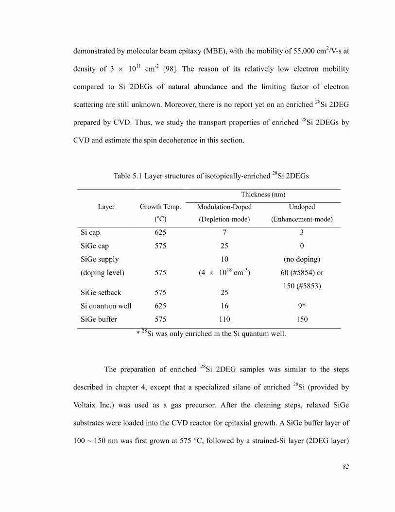
Table 5.1 Layer structures of isotopically-enriched 28Si 2DEGs
Thickness (nm)
Layer
Growth Temp.
(oC)
Modulation-Doped
(Depletion-mode)
Undoped
(Enhancement-mode)
Si cap 625 7 3
SiGe cap 575 25
SiGe supply
(doping level)
575
10
(4 1018 cm-3)
SiGe setback 575 25
0
(no doping)
60 (#5854) or
150 (#5853)
Si quantum well 625 16 9*
SiGe buffer 575 110 150
* 28Si was only enriched in the Si quantum well.
The preparation of enriched 28Si 2DEG samples was similar to the steps
described in chapter 4, except that a specialized silane of enriched 28Si (provided by
Voltaix Inc.) was used as a gas precursor. After the cleaning steps, relaxed SiGe
substrates were loaded into the CVD reactor for epitaxial growth. A SiGe buffer layer of
100 ~ 150 nm was first grown at 575 °C, followed by a strained-Si layer (2DEG layer)
83
at 625 °C, a SiGe setback layer at 575 °C, a n-type SiGe supply layer at 575 °C, a SiGe
cap layer at 525 °C, and a Si cap layer at 625 °C (Table 5.1). There are two sets of
samples in this section. First, a depletion-mode device of modulation-doped 2DEG with
28Si enriched throughout the entire epitaxial growth (including Si and SiGe epitaxial
layers) was fabricated. For enhancement-mode samples, the supply layer was grown
without n-type doping and 28Si was only enriched in the Si QW layer.
5.2.1 Reduction of Spin-Carrying Isotope 29Si by 28Si Enrichment
The concentrations of three isotopes, 28Si, 29Si, and 30Si, and Ge vs. depth in a
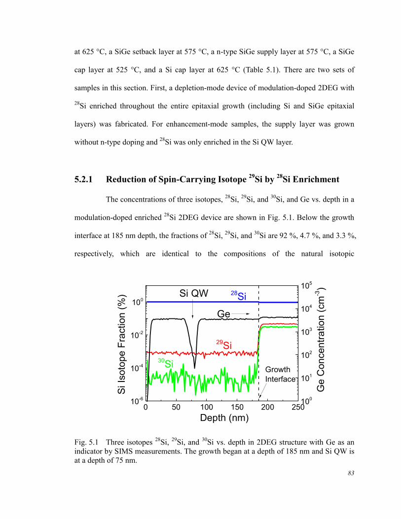
modulation-doped enriched 28Si 2DEG device are shown in Fig. 5.1. Below the growth
interface at 185 nm depth, the fractions of 28Si, 29Si, and 30Si are 92 %, 4.7 %, and 3.3 %,
respectively, which are identical to the compositions of the natural isotopic
0 50 100 150 200 25010-6
10-4
10-2
100Si QW
Ge
30Si
29Si
Si Is
oto
pe F
raction (
%)
Depth (nm)
28Si
GrowthInterface
100
101
102
103
104
105
Ge C
oncentr
ation (
cm
-3)
Fig. 5.1 Three isotopes 28Si, 29Si, and 30Si vs. depth in 2DEG structure with Ge as an indicator by SIMS measurements. The growth began at a depth of 185 nm and Si QW is at a depth of 75 nm.
84
10-3 10-2 10-1 100 101 10210-9
10-8
10-7
10-6
10-5
10-4
Assali's model
De
ph
asin
g T
ime
(se
c)
Fraction of 29Si (%)
Si QD [13]
GaAs QD [12]
Fig. 5.2 Dephasing time vs. 29Si fraction. Solid line is the model prediction, the solid square is the experimental result in Si QD [13], and the vertical dash line represents the fraction of 29Si in our enriched 28Si 2DEGs. Dephasing time of GaAs QDs [12] is also presented for comparison.
abundance [97]. For Si and SiGe epitaxial layers grown with silane of enriched 28Si,
the fractions for those three isotopes became 99.72 %, 0.08 %, and 0.002 %,
respectively. The enrichment factors, defined as the ratios of 28Si to 29Si and 28Si to
30Si, were increased from 20 to 1250 (i.e., 60 times enhancement), and 27 to 50,000
(i.e., 2000 times enhancement), respectively.
We now estimate the potential effects of 28Si enrichment on the spin
decoherence in Si QDs. By the enrichment of 28Si, the spin decoherence of QD electrons
from the nuclear spins of 29Si can be greatly suppressed. This would reduce the
dephasing time ( *2T ), which is dominated by the hyperfine interactions between nuclear
85
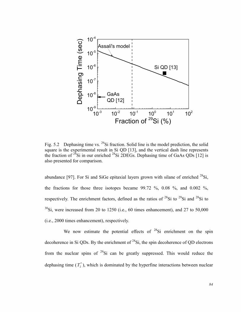
spins and electron spins. Assuming 105 nuclei in a Si QD of 100 nm 100 nm, Assali
et al. proposed a numerical model to estimate the dephasing time in Si [99]
11
5
*2 10
103.4
reT
(5.1)
where e is the electron charge and r is the fraction of 29Si. The predicted dephasing time
versus r was shown in Fig. 5.2 and compared with experimental results of a GaAs QD
and a Si QD of natural abundance. Maune et al. reported the first dephasing time of 360
ns in Si double QDs of natural abundance [13], which is 50 times longer than that in a
GaAs QD and very close to Assali’s prediction. In our sample, the fraction of 29Si was
purified by a factor of 20 to 0.08% and the dephasing time is expected to be 2 μs, two
orders of magnitude longer than that of a GaAs QD and 6 times longer than that of a Si
QD of natural abundance. According to the model, if 29Si can be reduced to 10 ppm, the
decoherence can be further reduced with *2T longer than 10 μs.
5.2.2 Magneto-Transport Properties of a Modulation-Doped
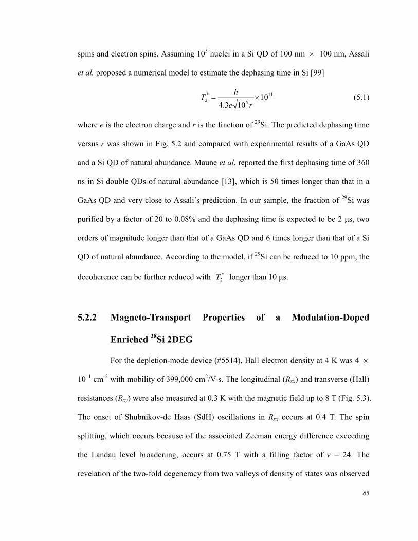
Enriched 28Si 2DEG
For the depletion-mode device (#5514), Hall electron density at 4 K was 4
1011 cm-2 with mobility of 399,000 cm2/V-s. The longitudinal (Rxx) and transverse (Hall)
resistances (Rxy) were also measured at 0.3 K with the magnetic field up to 8 T (Fig. 5.3).
The onset of Shubnikov-de Haas (SdH) oscillations in Rxx occurs at 0.4 T. The spin
splitting, which occurs because of the associated Zeeman energy difference exceeding
the Landau level broadening, occurs at 0.75 T with a filling factor of ν = 24. The
revelation of the two-fold degeneracy from two valleys of density of states was observed
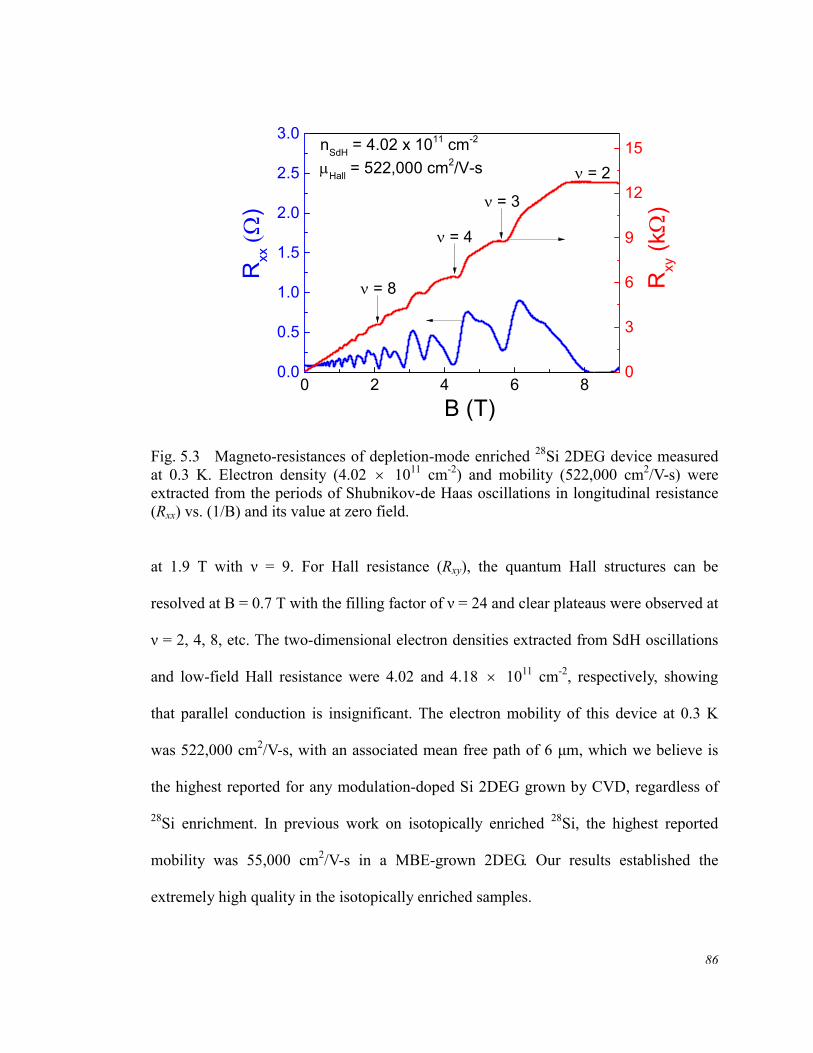
86
0 2 4 6 80.0
0.5
1.0
1.5
2.0
2.5
3.0
Rxx
)
B (T)
0
3
6
9
12
15
= 3
Rxy (
k
)
= 2
= 4
= 8
Hall
= 522,000 cm2/V-s
nSdH
= 4.02 x 1011 cm-2
Fig. 5.3 Magneto-resistances of depletion-mode enriched 28Si 2DEG device measured at 0.3 K. Electron density (4.02 1011 cm-2) and mobility (522,000 cm2/V-s) were extracted from the periods of Shubnikov-de Haas oscillations in longitudinal resistance (Rxx) vs. (1/B) and its value at zero field.
at 1.9 T with ν = 9. For Hall resistance (Rxy), the quantum Hall structures can be
resolved at B = 0.7 T with the filling factor of ν = 24 and clear plateaus were observed at
ν = 2, 4, 8, etc. The two-dimensional electron densities extracted from SdH oscillations
and low-field Hall resistance were 4.02 and 4.18 1011 cm-2, respectively, showing
that parallel conduction is insignificant. The electron mobility of this device at 0.3 K
was 522,000 cm2/V-s, with an associated mean free path of 6 μm, which we believe is
the highest reported for any modulation-doped Si 2DEG grown by CVD, regardless of
28Si enrichment. In previous work on isotopically enriched 28Si, the highest reported
mobility was 55,000 cm2/V-s in a MBE-grown 2DEG. Our results established the
extremely high quality in the isotopically enriched samples.
87
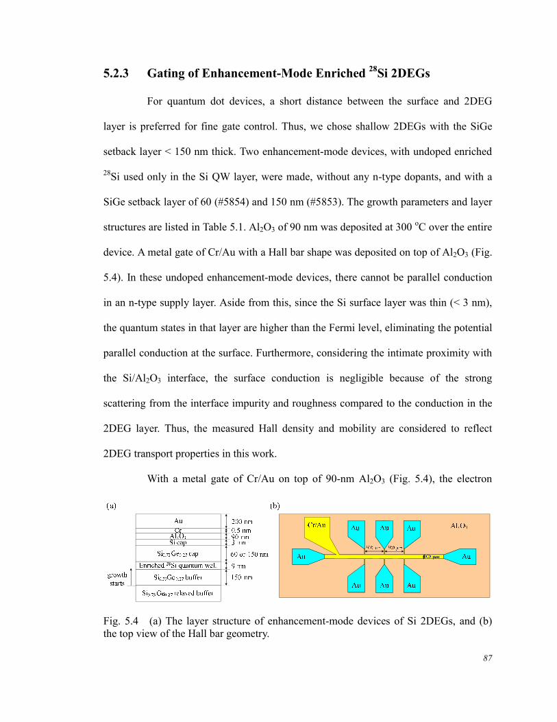
5.2.3 Gating of Enhancement-Mode Enriched 28Si 2DEGs
For quantum dot devices, a short distance between the surface and 2DEG
layer is preferred for fine gate control. Thus, we chose shallow 2DEGs with the SiGe
setback layer < 150 nm thick. Two enhancement-mode devices, with undoped enriched
28Si used only in the Si QW layer, were made, without any n-type dopants, and with a
SiGe setback layer of 60 (#5854) and 150 nm (#5853). The growth parameters and layer
structures are listed in Table 5.1. Al2O3 of 90 nm was deposited at 300 oC over the entire
device. A metal gate of Cr/Au with a Hall bar shape was deposited on top of Al2O3 (Fig.
5.4). In these undoped enhancement-mode devices, there cannot be parallel conduction
in an n-type supply layer. Aside from this, since the Si surface layer was thin (< 3 nm),
the quantum states in that layer are higher than the Fermi level, eliminating the potential
parallel conduction at the surface. Furthermore, considering the intimate proximity with
the Si/Al2O3 interface, the surface conduction is negligible because of the strong
scattering from the interface impurity and roughness compared to the conduction in the
2DEG layer. Thus, the measured Hall density and mobility are considered to reflect
2DEG transport properties in this work.
With a metal gate of Cr/Au on top of 90-nm Al2O3 (Fig. 5.4), the electron
Fig. 5.4 (a) The layer structure of enhancement-mode devices of Si 2DEGs, and (b) the top view of the Hall bar geometry.
88
2.0 2.5 3.0 3.50
1
2
3
4
5
setback: 60 nm
x 1011
nH
all (c
m-2)
Vg (V)
setback: 150 nm
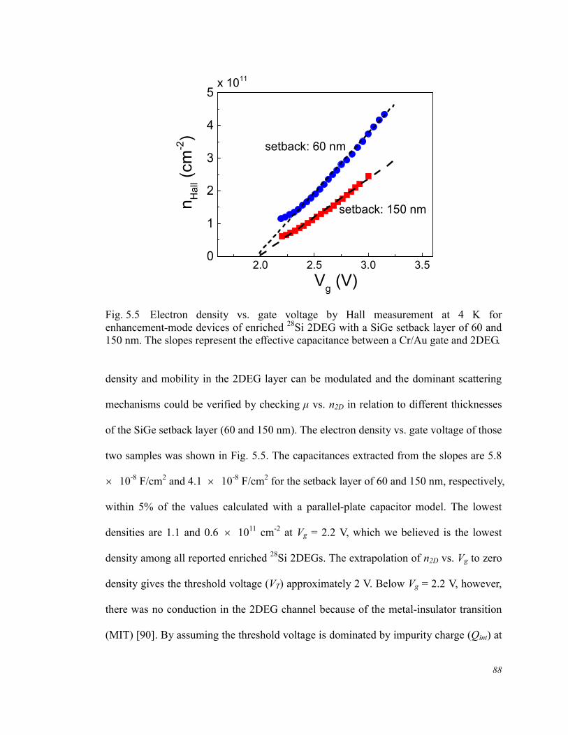
Fig. 5.5 Electron density vs. gate voltage by Hall measurement at 4 K for enhancement-mode devices of enriched 28Si 2DEG with a SiGe setback layer of 60 and 150 nm. The slopes represent the effective capacitance between a Cr/Au gate and 2DEG.
density and mobility in the 2DEG layer can be modulated and the dominant scattering
mechanisms could be verified by checking μ vs. n2D in relation to different thicknesses
of the SiGe setback layer (60 and 150 nm). The electron density vs. gate voltage of those
two samples was shown in Fig. 5.5. The capacitances extracted from the slopes are 5.8
10-8 F/cm2 and 4.1 10-8 F/cm2 for the setback layer of 60 and 150 nm, respectively,
within 5% of the values calculated with a parallel-plate capacitor model. The lowest
densities are 1.1 and 0.6 1011 cm-2 at Vg = 2.2 V, which we believed is the lowest
density among all reported enriched 28Si 2DEGs. The extrapolation of n2D vs. Vg to zero
density gives the threshold voltage (VT) approximately 2 V. Below Vg = 2.2 V, however,
there was no conduction in the 2DEG channel because of the metal-insulator transition
(MIT) [90]. By assuming the threshold voltage is dominated by impurity charge (Qint) at
89
1 2 3 4 5104
105
setback: 60 nm
Ha
ll (c
m2/V
-s)
nHall
(cm-2)
x 1011
setback: 150 nm
n1.7
Fig. 5.6 Hall mobility vs. density for enhancement-mode devices of enriched 28Si 2DEG with a SiGe setback layer of 60 and 150 nm at 4 K.
the Si/Al2O3 interface, a simple estimation can be made with Nint = Qint/e eVC TALO /
on the order of 1012 cm-2, where CALO is the capacitance (7.9 10-8 F/cm2) of 90-nm
Al2O3 dielectric layer assuming its relative dielectric constant is 8.
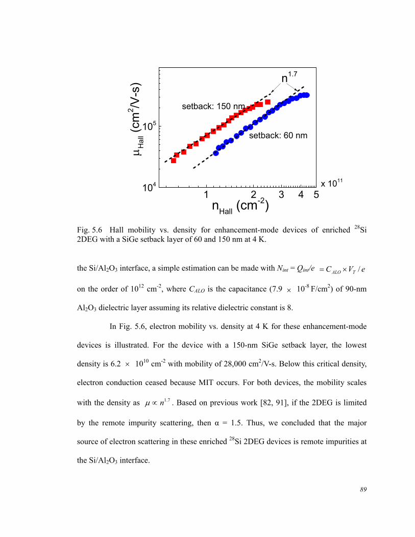
In Fig. 5.6, electron mobility vs. density at 4 K for these enhancement-mode
devices is illustrated. For the device with a 150-nm SiGe setback layer, the lowest
density is 6.2 1010 cm-2 with mobility of 28,000 cm2/V-s. Below this critical density,
electron conduction ceased because MIT occurs. For both devices, the mobility scales
with the density as 7.1n . Based on previous work [82, 91], if the 2DEG is limited
by the remote impurity scattering, then α = 1.5. Thus, we concluded that the major
source of electron scattering in these enriched 28Si 2DEG devices is remote impurities at
the Si/Al2O3 interface.
90
5.3 Inverted Modulation-Doped Si 2DEGs
In chapter 4, the remote impurity charges in the supply layer were suggested
to be the dominant scattering sources in a modulation-doped device of Si 2DEG, with
the supply layer on top of the Si QW layer. Due to a fast turn-on, the level of n-type
dopants is low in the setback layer, and the effects of impurity scattering between the
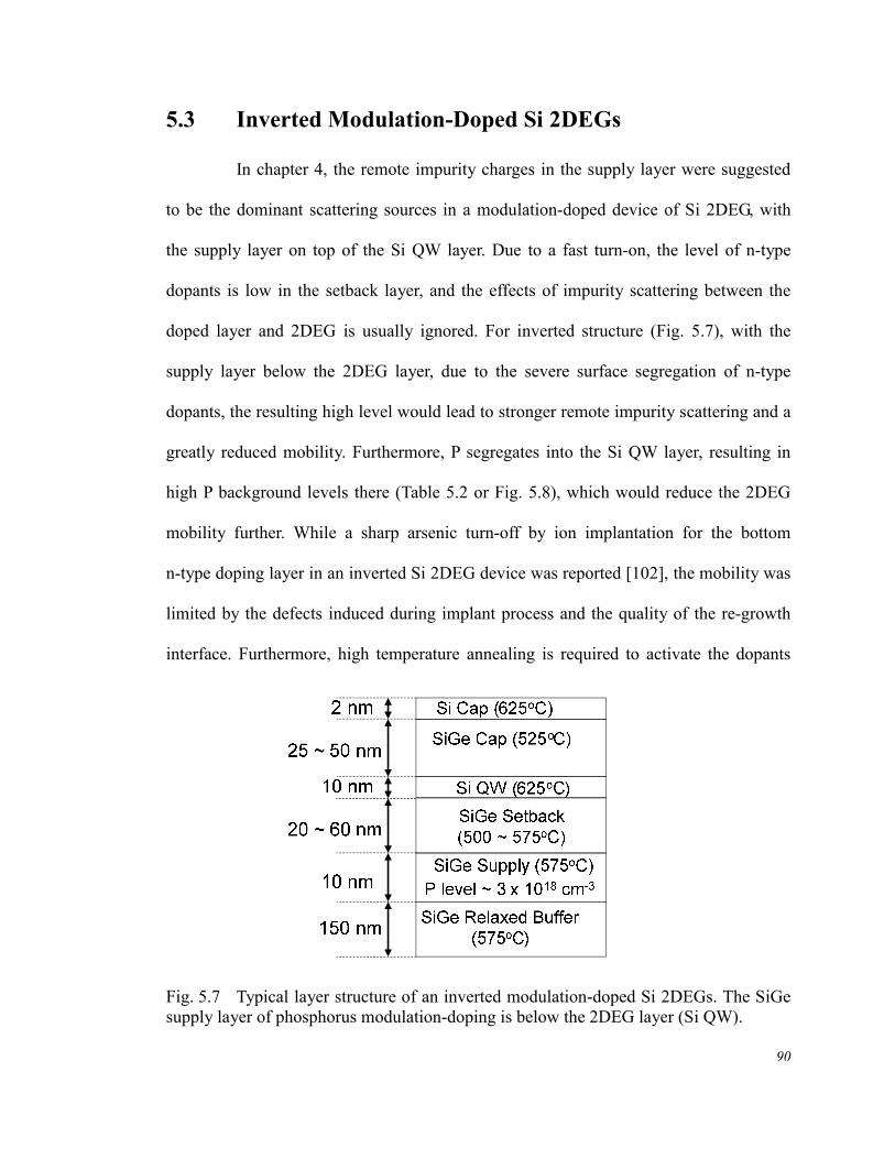
doped layer and 2DEG is usually ignored. For inverted structure (Fig. 5.7), with the
supply layer below the 2DEG layer, due to the severe surface segregation of n-type
dopants, the resulting high level would lead to stronger remote impurity scattering and a
greatly reduced mobility. Furthermore, P segregates into the Si QW layer, resulting in
high P background levels there (Table 5.2 or Fig. 5.8), which would reduce the 2DEG
mobility further. While a sharp arsenic turn-off by ion implantation for the bottom
n-type doping layer in an inverted Si 2DEG device was reported [102], the mobility was
limited by the defects induced during implant process and the quality of the re-growth
interface. Furthermore, high temperature annealing is required to activate the dopants
Fig. 5.7 Typical layer structure of an inverted modulation-doped Si 2DEGs. The SiGe supply layer of phosphorus modulation-doping is below the 2DEG layer (Si QW).
91
and remove the defects by implant, which would induce strain relaxation and increase
the thermal budget for the subsequent processing steps. By low-temperature epitaxy
(chapter 3), the phosphorus segregation can be significantly reduced with a sharp
turn-off, enabling a low level in the setback layer. Thus, sample #5457, #5850, and
#5630. P turn-off slopes of these three samples are 40, 14, and 8 nm/dec, respectively.
The setback layer thicknesses between the phosphorus peak level and the lower Si/SiGe
heterojunction are 20, 20, and 33 nm for those three in the final part of this thesis, we
investigate the effect of phosphorus segregation on 2DEG characteristics and present the
highest reported mobility of 470,000 cm2/V-s for all inverted modulation-doped Si
2DEGs.
5.3.1 Effects of Phosphorus Turn-Off Slope on 2DEG Mobility
To investigate the effects of phosphorus segregation on 2DEG properties in an
inverted structure, three samples of different phosphorus turn-off slopes (40, 14, and 8
nm/decade) were grown at different temperatures. The details of the layer structures are
listed in Table 5.2 and the associated SIMS results are illustrated in Fig. 5.8. For those
three samples, the thickness of the setback layer is defined as the distance between the
phosphorus peak and the lower Si/SiGe heterojunction. Hall electron density and
mobility measured at 4 K are plotted versus the phosphorus turn-off slope in Fig. 5.9.
The Hall electron densities of sample #5457, #5850, and #5630 are 3.8
1012 cm-2, 7 1011 cm-2, 1.8 1011 cm-2, respectively. As P turn-off slope increases,
there is more phosphorus in the SiGe setback layer, which would effectively reduce the
setback layer thickness by transferring electrons at shorter distances. Furthermore, high
92
P background levels in the Si QW layer might contribute more electrons in the 2DEG
layer. Thus, with the same setback layer thickness of 20 nm, the density of #5457 with P
turn-off slope of 40 nm/dec is higher than that of #5850 with P turn-off slope of 12
nm/dec. For #5630 of a thicker setback layer, the P turn-off slope is 8 nm/dec and the P
level is very low (below the detection limit), so the electron density is less than those of
#5457 and #5850.
Table 5.2 Layer structures of sample #5457, #5850, and #5630 for study of the effects of P turn-off slope on 2DEG characteristics in an inverted modulation-doped structure.
Sample # 5457 5850 5630
Si cap (nm) @ 625oC 5 3 2.5
SiGe cap (nm) @ 575oC 46 38 50
Si QW (nm) @ 625oC
P level in Si QW
12
0.6 ~ 21018 cm-3
11
1 ~ 21017 cm-3
11
below 51015 cm-3
(SIMS limit)
SiGe setback (nm)
P turn-off slope
growth temperature
20
40 nm/dec
575 oC
20
14 nm/dec
525 oC
33
8 nm/dec
500 oC
P Peak level (cm-3) 4.8 1018 3.3 1018 4.6 1018
SiGe buffer (nm) @ 575oC 160 125 170
0 25 50 75 100 125 150 175 2001015
1016
1017
1018
1019
1020
Ge
P C
oncentr
ation (
cm
-3)
Depth (nm)
P40 nm/dec
0
10
20
30
40
Ge F
raction (
%)
0 25 50 75 100 125 150 175 2001015
1016
1017
1018
1019
1020
Ge
P C
oncentr
ation (
cm
-3)
Depth (nm)
P12 nm/dec
0
10
20
30
40
Ge F
raction (
%)
0 25 50 75 100 125 150 175 2001015
1016
1017
1018
1019
1020
Ge
P C
oncentr
ation (
cm
-3)
Depth (nm)
P
8 nm/dec
0
10
20
30
40
Ge F
raction (
%)
Fig. 5.8 P and Ge profiles of sample #5457, #5850, and #5630. P turn-off slopes of these three samples are 40, 14, and 8 nm/dec, respectively. The setback layer thicknesses between the phosphorus peak level and the lower Si/SiGe heterojunction are 20, 20, and 33 nm for those three samples.
93
0 10 20 30 40 50103
104
105
(
cm
2/V
-s)
P Turn-Off Slope (nm/dec)
1011
1012
1013
nH
all (c
m-2)
Fig. 5.9 Hall density and mobility vs. P turn-off slope for sample #5457 (40 nm/dec), #5850 (14 nm/dec), and #5630 (8 nm/dec). A corrected electron density was calculated by Poisson’s equation to compensate the effect of the thicker SiGe setback layer in sample # 5630.
2DEG mobility is also affected greatly by phosphorus turn-off slope (Fig. 5.9).
With a fast phosphorus turn-off slope of 8 nm/dec in sample #5630, the mobility is
60,000 cm2/V-s, 20 times higher than that of sample #5457 with a slow slope of 40
nm/dec. For sample #5457, even though electron screening is expected to be stronger
than sample #5630 because of the higher electron density (3.8 1012 cm-2 >> 1.8
1011 cm-2), the mobility is actually much lower. This is attributed to the high level of
phosphorus in the setback layer because of a slow phosphorus turn-off, introducing
stronger remote impurity scattering for 2DEG. Furthermore, for the sample of a slow P
turn-off such as #5457, the resulting high P level of 1018 cm-3 in the Si QW layer could
cause stronger background impurity scattering. Both remote and background impurity
scattering affect the 2DEG mobility in the inverted modulation-doped Si 2DEGs with
slow P turn-off. Thus, a fast P turn-off must be used for high-mobility 2DEGs.
94
5.3.2 Effects of Remote Impurity at the Si/Al2O3 Interface on
Mobility
In this section, we study the effect of the impurity charges at the Si/Al2O3
interface. Unlike a top modulation-doped Si 2DEG with ionized impurities in the supply
layer to screen the remote charges at the Si surface, in an inverted structure, the remote
scattering effect of the Si surface charges must be considered because of the absence of
an n-type doping layer between the surface and 2DEG. If the charge density at the
surface is higher than the remote impurity charge in the bottom supply layer in an
inverted 2DEG device, presumably, the mobility would be largely affected by those
unscreened surface charges [89]. By reducing the surface charge density or the distance
between the surface and 2DEG [73], the scattering is expected to be weaker.
Table 5.3 Layer structures of sample #5877 and #5630 for study of the effects of impurity charges at the Si/Al2O3 interface on 2DEG mobility.
Sample # 5877 5630
Si cap (nm) @ 625oC 3 2.5
SiGe cap (nm) @ 575oC 26 50
Si QW (nm) @ 625oC
P level in QW (cm-3)
11
below 5 1015
11
below 5 1015
SiGe setback (nm)
P turn-off slope
62
13 nm/dec; @ 525 oC
33
8 nm/dec; @ 500 oC
P Peak level (cm-3) 2.5 1018 4.6 1018
SiGe buffer (nm) @575oC 115 170
Hall bar devices with a Cr/Au/Al2O3 gate stack on top of inverted
modulation-doped Si 2DEGs (Fig. 5.4) were fabricated to investigate the effect of the
95
0 25 50 75 100 125 150 175 2001015
1016
1017
1018
1019
1020
Ge
P C
oncentr
ation (
cm
-3)
Depth (nm)
P
8 nm/dec
0
10
20
30
40
Ge
Fra
ctio
n (
%)
0 25 50 75 100 125 150 175 2001015
1016
1017
1018
1019
1020
GeP
Concentr
ation (
cm
-3)
Depth (nm)
P
12 nm/dec
0
10
20
30
40
Ge
Fra
ctio
n (
%)
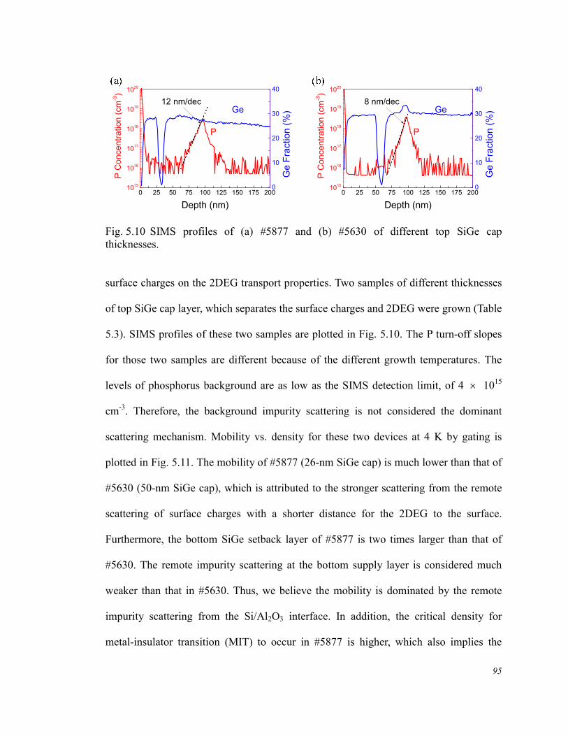
Fig. 5.10 SIMS profiles of (a) #5877 and (b) #5630 of different top SiGe cap thicknesses.
surface charges on the 2DEG transport properties. Two samples of different thicknesses
of top SiGe cap layer, which separates the surface charges and 2DEG were grown (Table
5.3). SIMS profiles of these two samples are plotted in Fig. 5.10. The P turn-off slopes
for those two samples are different because of the different growth temperatures. The
levels of phosphorus background are as low as the SIMS detection limit, of 4 1015
cm-3. Therefore, the background impurity scattering is not considered the dominant
scattering mechanism. Mobility vs. density for these two devices at 4 K by gating is
plotted in Fig. 5.11. The mobility of #5877 (26-nm SiGe cap) is much lower than that of
#5630 (50-nm SiGe cap), which is attributed to the stronger scattering from the remote
scattering of surface charges with a shorter distance for the 2DEG to the surface.
Furthermore, the bottom SiGe setback layer of #5877 is two times larger than that of
#5630. The remote impurity scattering at the bottom supply layer is considered much
weaker than that in #5630. Thus, we believe the mobility is dominated by the remote
impurity scattering from the Si/Al2O3 interface. In addition, the critical density for
metal-insulator transition (MIT) to occur in #5877 is higher, which also implies the
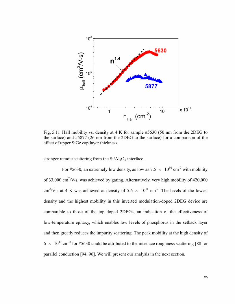
96
1 10104
105
106
5877
x 1011
hall (c
m2/V
-s)
nHall
(cm-2)
5630
n1.4
Fig. 5.11 Hall mobility vs. density at 4 K for sample #5630 (50 nm from the 2DEG to the surface) and #5877 (26 nm from the 2DEG to the surface) for a comparison of the effect of upper SiGe cap layer thickness.
stronger remote scattering from the Si/Al2O3 interface.
For #5630, an extremely low density, as low as 7.5 1010 cm-2 with mobility
of 33,000 cm2/V-s, was achieved by gating. Alternatively, very high mobility of 420,000
cm2/V-s at 4 K was achieved at density of 5.6 1011 cm-2. The levels of the lowest
density and the highest mobility in this inverted modulation-doped 2DEG device are
comparable to those of the top doped 2DEGs, an indication of the effectiveness of
low-temperature epitaxy, which enables low levels of phosphorus in the setback layer
and then greatly reduces the impurity scattering. The peak mobility at the high density of
6 1011 cm-2 for #5630 could be attributed to the interface roughness scattering [88] or
parallel conduction [94, 96]. We will present our analysis in the next section.
97
5.3.3 Second Subband Occupancy
In a gated device, a maximum in mobility was observed at the density of
mid-1011 cm-2 in GaAs 2DEGs because of the interface roughness scattering [88] or
parallel conduction [94, 96]. For an enhancement-mode Si 2DEG device, the interface
roughness scattering was suggested by Huang et al. to account for the presence of peak
in the mobility [73]. While their results could be fit by a model with several adjustable
parameters, it was suggested that in modulation-doped GaAs 2DEGs, the contribution of
parallel conduction in other channels such as the doped layer or the second subband in
the QW layer would dominate over the interface roughness scattering [63]. This was
confirmed by the experimental results of Shubnikov-de Haas oscillations, showing the
presence of the parallel conduction in GaAs 2DEGs [103, 104, 105]. Some of the gated
devices in this work showed maximum mobility. Thus, we present the analysis of
sample #5630 with a peak mobility at density of 6 1011 cm-2 (Fig. 5.11) and report
the first experimental observation of second subband occupancy in a Si 2DEG.
First, Hall density (nHall) and mobility (μHall) vs. gate voltage at 0.3 K of
sample #5630 is shown in Fig. 5.12. The device is conducting at Vg > 1.8 V with a
threshold voltage of 1.45 V by extrapolating nHall vs. Vg to nHall = 0 (red dash line in Fig.
5.12). Between 1.45 V and 1.8 V, there was no conduction because of the metal-insulator
transition. When the channel conducts, the Hall electron density increases with gate
voltage. The extracted slope of the Hall density gives the effective capacitance of 6
10-8 F/cm2 between the Cr/Au gate and the 2DEG layer, which is close to the calculated
value of 5.8 10-8 F/cm2, based on the parallel capacitor model. Note there is a kink in
nHall at Vg = 3.4 V, beyond which the predicted density (red dash line in Fig. 5.12 (a)) is
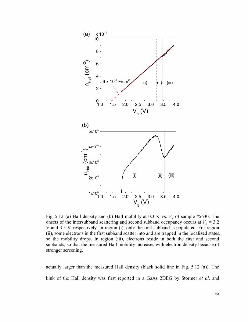
98
1.0 1.5 2.0 2.5 3.0 3.5 4.00
2
4
6
8
10
(i) (ii) (iii)nH
all (c
m-2)
Vg (V)
6 x 10⁻⁸ F/cm2
x 1011(a)
1.0 1.5 2.0 2.5 3.0 3.5 4.01x10⁵
2x10⁵
3x10⁵
4x10⁵
5x10⁵
H
all (c
m-2)
Vg (V)
(i) (ii) (iii)
(b)
Fig. 5.12 (a) Hall density and (b) Hall mobility at 0.3 K vs. Vg of sample #5630. The onsets of the intersubband scattering and second subband occupancy occurs at Vg = 3.2 V and 3.5 V, respectively. In region (i), only the first subband is populated. For region (ii), some electrons in the first subband scatter into and are trapped in the localized states, so the mobility drops. In region (iii), electrons reside in both the first and second subbands, so that the measured Hall mobility increases with electron density because of stronger screening.
actually larger than the measured Hall density (black solid line in Fig. 5.12 (a)). The
kink of the Hall density was first reported in a GaAs 2DEG by Störmer et al. and
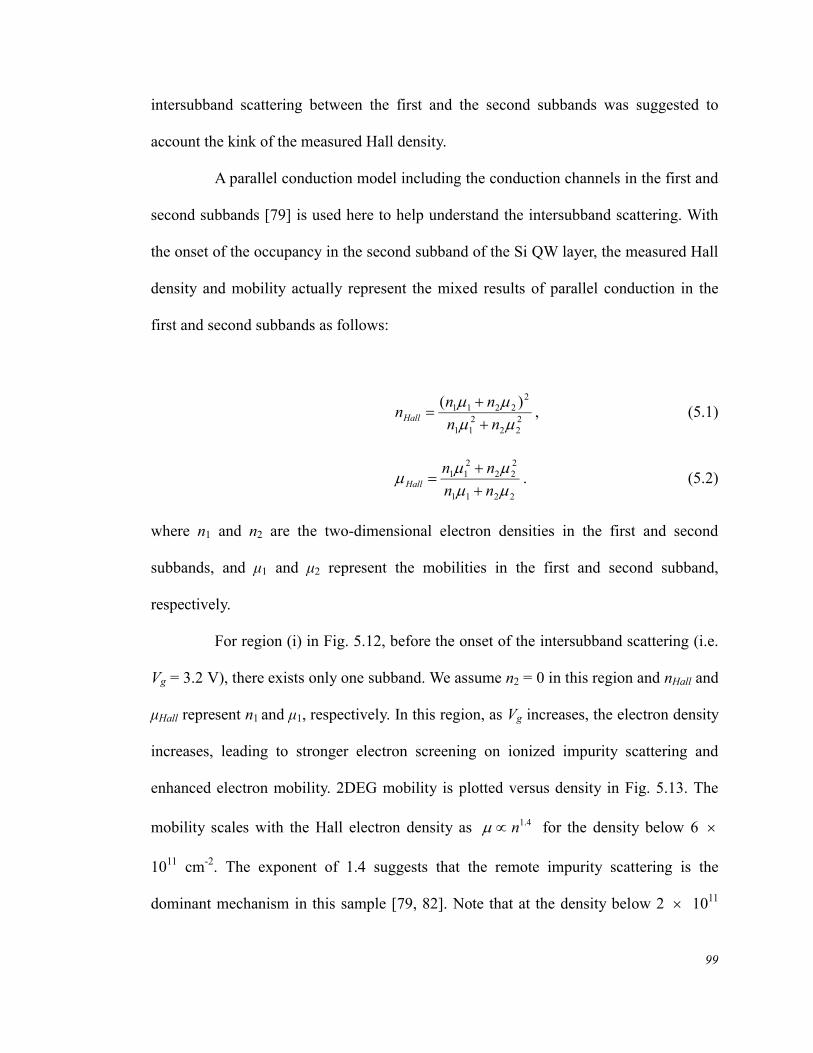
99
intersubband scattering between the first and the second subbands was suggested to
account the kink of the measured Hall density.
A parallel conduction model including the conduction channels in the first and
second subbands [79] is used here to help understand the intersubband scattering. With
the onset of the occupancy in the second subband of the Si QW layer, the measured Hall
density and mobility actually represent the mixed results of parallel conduction in the
first and second subbands as follows:
222
211
22211 )(
nn
nnnHall
, (5.1)
2211
222
211
nn
nnHall
. (5.2)
where n1 and n2 are the two-dimensional electron densities in the first and second
subbands, and μ1 and μ2 represent the mobilities in the first and second subband,
respectively.
For region (i) in Fig. 5.12, before the onset of the intersubband scattering (i.e.
Vg = 3.2 V), there exists only one subband. We assume n2 = 0 in this region and nHall and
μHall represent n1 and μ1, respectively. In this region, as Vg increases, the electron density
increases, leading to stronger electron screening on ionized impurity scattering and
enhanced electron mobility. 2DEG mobility is plotted versus density in Fig. 5.13. The
mobility scales with the Hall electron density as 4.1n for the density below 6
1011 cm-2. The exponent of 1.4 suggests that the remote impurity scattering is the
dominant mechanism in this sample [79, 82]. Note that at the density below 2 1011
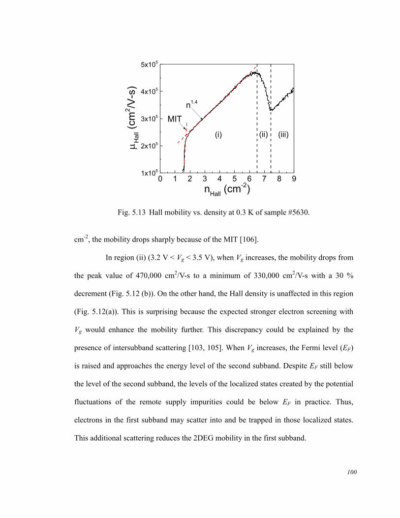
100
0 1 2 3 4 5 6 7 8 91x105
2x10⁵
3x10⁵
4x10⁵
5x10⁵
(iii)(ii)
Ha
ll (c
m2/V
-s)
nHall
(cm-2)
(i)
MIT
n1.4
Fig. 5.13 Hall mobility vs. density at 0.3 K of sample #5630.
cm-2, the mobility drops sharply because of the MIT [106].
In region (ii) (3.2 V < Vg < 3.5 V), when Vg increases, the mobility drops from
the peak value of 470,000 cm2/V-s to a minimum of 330,000 cm2/V-s with a 30 %
decrement (Fig. 5.12 (b)). On the other hand, the Hall density is unaffected in this region
(Fig. 5.12(a)). This is surprising because the expected stronger electron screening with
Vg would enhance the mobility further. This discrepancy could be explained by the
presence of intersubband scattering [103, 105]. When Vg increases, the Fermi level (EF)
is raised and approaches the energy level of the second subband. Despite EF still below
the level of the second subband, the levels of the localized states created by the potential
fluctuations of the remote supply impurities could be below EF in practice. Thus,
electrons in the first subband may scatter into and be trapped in those localized states.
This additional scattering reduces the 2DEG mobility in the first subband.
101
To quantitatively explain this argument, we assume there are two conduction
channels of electrons in region (ii): the first subband and the localized states of the
second subband. Since electrons in the localized states are trapped, we assume μlocal = 0,
so nHall and μHall in Eqs. (5.1) and (5.2) represent n1 and μ1, respectively. While nHall (=
n1) increases with Vg, μHall drops as Vg increases (Fig. 5.12 (b)). Since μlocal = 0, the
measured Hall mobility represents the true 2DEG mobility in the first subband. With the
presence of the localized states, electrons in the first subband can scatter into those
localized states and be trapped, so μHall (= μ1) drops.
In region (iii), as EF is lifted further by increasing Vg, the localized states are
filled and mobile electrons start to populate the second subband. nHall and μHall represent
the combined density and mobility of the first and second subbands following Eqs. (5.1)
and (5.2). Since the FFT spectrums of Rxx from this sample were too noisy, a quantitative
measure of the population process in the first and second subbands is not possible.
However, following Störmer’s arguments, we assume that when the Fermi level enters
the second subband, n2 increases with Vg and n1 is constant [103]. For μ1 and μ2, both
increases with Vg because of stronger screening by more populated electrons in the
second subband. Since both μ1 and μ2 could be functions of n2, it is not possible to solve
them simultaneously without the information of the density in the second subband.
Here, we present a simplified analysis of two channel conduction in region
(iii). Assuming above Vg = 3.5 V (Fig. 5.12 (b)), the first subband and the localized
states of the second subband are fully populated. When Vg increases, electrons are
injected into the second subband and the relationship of n2 and Vg follows a simple
parallel-plate capacitor model. Thus, above 3.5 V, n2 increases from zero with an
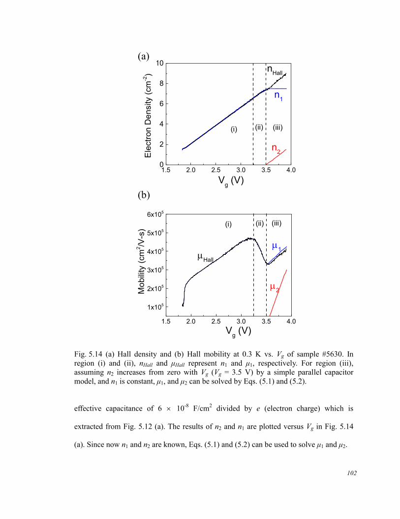
102
1.5 2.0 2.5 3.0 3.5 4.00
2
4
6
8
10n
Hall
n2
Ele
ctr
on D
ensity (
cm
-2)
Vg (V)
n1
(iii)(ii)(i)
1.5 2.0 2.5 3.0 3.5 4.0
1x10⁵
2x10⁵
3x10⁵
4x10⁵
5x10⁵
6x10⁵
2
1
Vg (V)
Mo
bili
ty (
cm
2/V
-s)
Hall
(iii)(ii)(i)
Fig. 5.14 (a) Hall density and (b) Hall mobility at 0.3 K vs. Vg of sample #5630. In region (i) and (ii), nHall and μHall represent n1 and μ1, respectively. For region (iii), assuming n2 increases from zero with Vg (Vg = 3.5 V) by a simple parallel capacitor model, and n1 is constant, μ1, and μ2 can be solved by Eqs. (5.1) and (5.2).
effective capacitance of 6 10-8 F/cm2 divided by e (electron charge) which is
extracted from Fig. 5.12 (a). The results of n2 and n1 are plotted versus Vg in Fig. 5.14
(a). Since now n1 and n2 are known, Eqs. (5.1) and (5.2) can be used to solve μ1 and μ2.
(a)
(b)
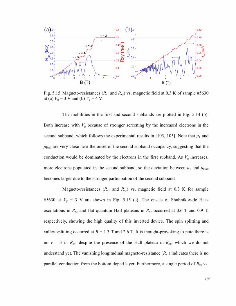
103
0 2 4 6 8 10 120.0
0.5
1.0
1.5
2.0
2.5
3.0
3.5
4.0
Rxx (
k
)
B (T)
0.0
0.1
0.2
0.3
0.4
0.5
0.6
= 5
= 3
= 4
Rxy (
h/e
2)
= 2
0 1 2 3 40.0
0.2
0.4
0.6
0.8
1.0
Rxx (
k
)
B (T)
0.00
0.02
0.04
0.06
0.08
0.10
0.12
Rxy (
h/e
2)
Fig. 5.15 Magneto-resistances (Rxx and Rxy) vs. magnetic field at 0.3 K of sample #5630 at (a) Vg = 3 V and (b) Vg = 4 V.
The mobilities in the first and second subbands are plotted in Fig. 5.14 (b).
Both increase with Vg because of stronger screening by the increased electrons in the
second subband, which follows the experimental results in [103, 105]. Note that μ1 and
μHall are very close near the onset of the second subband occupancy, suggesting that the
conduction would be dominated by the electrons in the first subband. As Vg increases,
more electrons populated in the second subband, so the deviation between μ1 and μHall
becomes larger due to the stronger participation of the second subband.
Magneto-resistances (Rxx and Rxy) vs. magnetic field at 0.3 K for sample
#5630 at Vg = 3 V are shown in Fig. 5.15 (a). The onsets of Shubnikov-de Haas
oscillations in Rxx and flat quantum Hall plateaus in Rxy occurred at 0.6 T and 0.9 T,
respectively, showing the high quality of this inverted device. The spin splitting and
valley splitting occurred at B = 1.3 T and 2.6 T. It is thought-provoking to note there is
no ν = 3 in Rxx, despite the presence of the Hall plateau in Rxy, which we do not
understand yet. The vanishing longitudinal magneto-resistance (Rxx) indicates there is no
parallel conduction from the bottom doped layer. Furthermore, a single period of Rxx vs.
(a) (b)
104
(1/B) suggests only one two-dimensional channel exists. As the gate voltage increases,
the presence of the beating of the oscillations in Rxx indicates the onset of the occupancy
of the second subband (Fig. 5.15 (b)).
5.3.4 Comparison of 2DEG Mobility in Different Structures
In this thesis, we studied three different structures of Si 2DEGs: standard
modulation-doped Si 2DEG (with a doping layer on top of the Si QW), an inverted
modulation-doped Si 2DEG (with a doping layer on the bottom of the Si QW), and an
enhancement-mode 28Si enriched 2DEG without any doping layer. The relationship of μ
and n at 4 K for those structures are plotted in Fig. 5.16 with the results of
enhancement-mode 2DEG of natural Si also shown for comparison (courtesy of
Chiao-Ti Huang). Clearly, at electron density below 3 1011 cm-2, the mobilities for all
structures are almost identical with a slope of 5.1n . For those four structures, the
distance from the 2DEG to the surface is 50 ~ 60 nm regardless of the presence of the
doping layers except top-doped sample (#5737) with a distance of 100 nm from the
surface to the 2DEG and a distance of 50 nm from the remote doped layer to the
underlying 2DEG (Fig. 4.19(a)).
Based on the prior theoretical or experimental work [82, 91], if the exponent
of n is close to 1.5, it is suggested the remote impurity scattering would be the
dominant scattering mechanism. In Fig. 5.16, all curves of mobility vs. density show
their exponents close to 1.5, which seems support our arguments on the limiting
scattering mechanism. For quantum dot applications, a low electron density of ~ 1
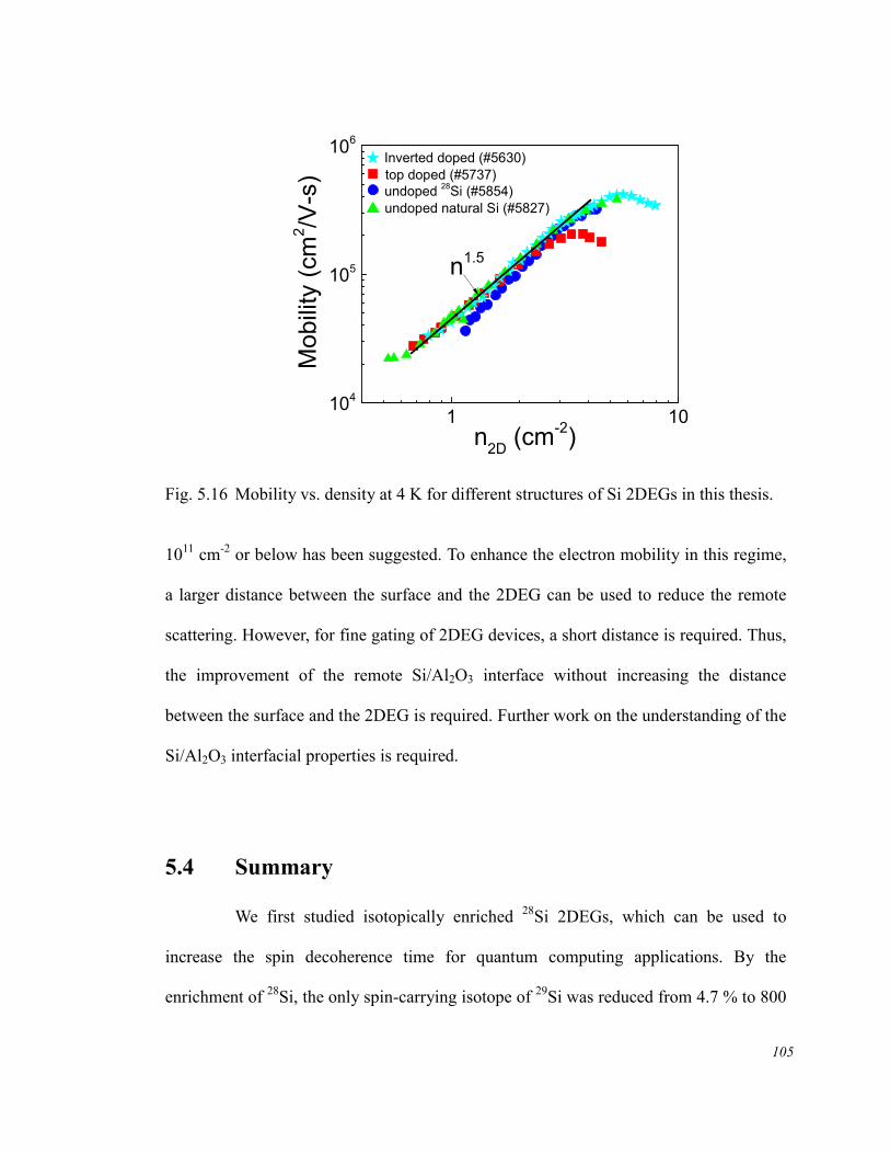
105
1 10104
105
106
undoped natural Si (#5827)undoped
28Si (#5854)
top doped (#5737)
Mo
bili
ty (
cm
2/V
-s)
n2D
(cm-2)
n1.5
Inverted doped (#5630)
Fig. 5.16 Mobility vs. density at 4 K for different structures of Si 2DEGs in this thesis.
1011 cm-2 or below has been suggested. To enhance the electron mobility in this regime,
a larger distance between the surface and the 2DEG can be used to reduce the remote
scattering. However, for fine gating of 2DEG devices, a short distance is required. Thus,
the improvement of the remote Si/Al2O3 interface without increasing the distance
between the surface and the 2DEG is required. Further work on the understanding of the
Si/Al2O3 interfacial properties is required.
5.4 Summary
We first studied isotopically enriched 28Si 2DEGs, which can be used to
increase the spin decoherence time for quantum computing applications. By the
enrichment of 28Si, the only spin-carrying isotope of 29Si was reduced from 4.7 % to 800
106
ppm with a predicted dephasing time of 2 μs. Furthermore, a high mobility of 522,000
cm2/V-s at 0.3 K in an enriched 28Si 2DEG was reported with clear Hall plateaus and
Shubnikov-de Haas oscillations, showing its high material quality. By top gating, remote
impurity charges at the Si/Al2O3 interface was suggested as the dominant scattering
source, and an extremely low free electron density of 6 1010 cm-2 was also presented.
Then we present an inverted modulation-doped Si 2DEGs of high mobility ~
470,000 cm2/V-s at 0.3 K by the suppression of phosphorus segregation in the lower
SiGe setback layer. We showed that the sharp P turn-off (< 10 nm/decade) is a key to the
success of high-quality inverted structures. An inverted modulation-doped Si 2DEG of
high mobility by reducing phosphorus segregation opens the path towards the first
demonstration of a bilayer device of two adjacent Si 2DEGs. Second subband
occupancy and the intersubband scattering of electron between the first and second
subbands were also demonstrated for the first time in a Si 2DEG.
It is interesting to note that μ vs. n, in a enhancement-mode structure Si 2DEG
of isotopically enriched 28Si, in a enhancement-mode 2DEG of natural Si, in a standard
modulation-doped (top-doped) Si 2DEG, and in a inverted modulation-doped
(bottom-doped) Si 2DEG, all with the distance of 50 ~ 60 nm from the 2DEG layer to
the remote impurity layer such as the supply layer or the Si surface layer, shows a
strikingly similar form. It seems electron mobility was limited by the remote impurity
scattering at the Si surface.
107
Chapter 6 Conclusions and Future Work
6.1 Conclusions
Strained Si and SiGe quantum devices were made from structures grown by CVD. First,
we presented the work of band-to-band tunneling in strained SiGe, which is crucial for
Si-based tunneling FETs for low-power applications. We investigated the effects of
electric field and Ge fraction on band-to-band tunneling (BTBT) in p+-SiGe/n+-Si
heterojunctions and p+-SiGe/n+-SiGe homojunctions at both forward and reverse biases.
Negative differential resistance (NDR) was observed for each device, showing the high
quality of tunneling devices by CVD. A peak current density of 8.2 kA/cm2 in forward
bias and reverse-biased BTBT current density of 103 kA/cm2 at -1 V were demonstrated,
both of which we believed to be the highest among all Si-based tunneling diodes by
CVD. Furthermore, we also showed the importance of the presence of NDR in forward
bias to distinguish between direct BTBT and defect-assisted tunneling in reverse bias.
Good agreement between experimental results and models for forward and reverse
biases was achieved, which can serve as a basis for the related tunneling device
modeling.
Next, we studied the surface segregation of phosphorus in relaxed SiGe
epitaxial layers and investigated the effects of surface hydrogen. We experimentally
observed an opposite trend of phosphorus segregation versus temperature compared to
that expected from the prediction of a two-state model (TSM). We proposed a
phenomenological model that accounts for the effect of surface hydrogen on the
108
segregation energy of phosphorus. Surface hydrogen changes the bonding structure of
host atoms (Si or Ge) in the surface layer and reduces the segregation energy. An
extremely sharp P turn-off slope of 6 nm/dec was also achieved, enabling effective
Schottky gating on modulation-doped Si two-dimensional electron gas.
Two-dimensional electron gases (2DEGs) in a strained Si are promising for
quantum dot applications. We investigated the transport properties in Si 2DEGs grown
in Princeton and achieved a mobility of 522,000 cm2/V-s at 0.3 K, among the best by
CVD. This was attributed to the reduction of the phosphorus background level in the
CVD system by a gas separation system of the doping gas of phosphorus and other
process gases. The effects of different layers on ungated depletion-mode devices of
modulation-doped Si 2DEG were investigated. The results showed that the remote
impurity charges at the supply layer were the major source of electron scattering. The
experimental results of top Schottky gated devices also supported this conclusion.
In Si of natural abundance, only the 4.7 % atoms of 29Si carry nuclear spins,
leading to spin decoherence. 28Si enrichment reduced the level of 29Si to 800 ppm, which
could extend the dephasing time in QDs to 2μs, 300 times longer than that in GaAs QDs.
High mobility of 522,000 cm2/V-s in an isotopically enriched 28Si 2DEG was also
reported. The remote impurity charges at the supply layer for the depletion-mode
devices and at the Si/Al2O3 interface for the enhancement-mode devices were
considered the main source for electron scattering.
Last, an inverted modulation-doped 2DEG with Si of natural abundance
achieved a record high mobility of 470,000 cm2/V-s at 0.3 K. High mobility in this type
of structure was attributed to the lower phosphorus level by strong reduction of
109
phosphorus segregation, which was enabled by low-temperature epitaxy. Furthermore,
we experimentally presented the occupancy of the second subband and intersubband
scattering between the first and second subbands in a Si 2DEG for the first time. The
fact that the initial drop and subsequent rise in the measured Hall mobility because of
the intersubband scattering were observed supported our conclusions.
6.2 Future Work
In this section, some aspects of considerable interest about the topics in this
thesis are given as follows:
(i) Band-to-band tunneling devices:
Based on the results in chapter 2, SiGe-based BTBT is promising for the
realization of TFET of high performance. However, there is no report on any Si-based
TFET with a high drive current as high as 100 μA/μm and a sharp sub-threshold slope of
< 60 mV/decade at the same time, which is crucial for the replacement of conventional
MOSFETs. Further work on the comparison of the TFET experiment and modeling
based on our experimental results from diode structures will be required for further
development of TFETs.
(ii) Phosphorus segregation:
In chapter 2, phosphorus turn-off slopes in strained and relaxed Si0.7Ge0.3 films
were different. A further analysis is required to explain this observation. Moreover, since
the hydrogen coverage depends on the Ge fraction in SiGe alloys, the effect of hydrogen
110
on the bonding structure and segregation energy of phosphorus near the surface could
also be different for various Ge fractions.
(iii) Si 2DEG:
While high mobility in Si 2DEGs was demonstrated by our CVD, the predicted
upper limit of mobility is still much higher than our experimental results. Further work
is required to determine the missing factor. In addition, the process of second subband
occupancy is not completely understood, although some convincing evidence was
presented. Last, the high-mobility inverted modulation-doped Si 2DEG enables the
growth of a bilayer of parallel Si 2DEGs.
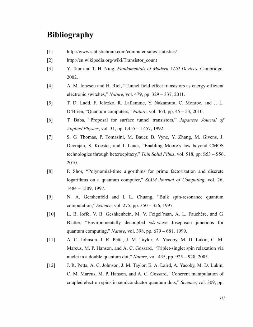
111
Bibliography
[1] http://www.statisticbrain.com/computer-sales-statistics/
[2] http://en.wikipedia.org/wiki/Transistor_count
[3] Y. Taur and T. H. Ning, Fundamentals of Modern VLSI Devices, Cambridge,
2002.
[4] A. M. Ionescu and H. Riel, “Tunnel field-effect transistors as energy-efficient
electronic switches,” Nature, vol. 479, pp. 329 – 337, 2011.
[5] T. D. Ladd, F. Jelezko, R. Laflamme, Y. Nakamura, C. Monroe, and J. L.
O’Brien, “Quantum computers,” Nature, vol. 464, pp. 45 – 53, 2010.
[6] T. Baba, “Proposal for surface tunnel transistors,” Japanese Journal of
Applied Physics, vol. 31, pp. L455 – L457, 1992.
[7] S. G. Thomas, P. Tomasini, M. Bauer, B. Vyne, Y. Zhang, M. Givens, J.
Devrajan, S. Koester, and I. Lauer, ”Enabling Moore’s law beyond CMOS
technologies through heteroepitaxy,” Thin Solid Films, vol. 518, pp. S53 – S56,
2010.
[8] P. Shor, “Polynomial-time algorithms for prime factorization and discrete
logarithms on a quantum computer,” SIAM Journal of Computing, vol. 26,
1484 – 1509, 1997.
[9] N. A. Gershenfeld and I. L. Chuang, “Bulk spin-resonance quantum
computation,” Science, vol. 275, pp. 350 – 356, 1997.
[10] L. B. Ioffe, V. B. Geshkenbein, M. V. Feigel’man, A. L. Fauchère, and G.
Blatter, “Environmentally decoupled sds-wave Josephson junctions for
quantum computing,” Nature, vol. 398, pp. 679 – 681, 1999.
[11] A. C. Johnson, J. R. Petta, J. M. Taylor, A. Yacoby, M. D. Lukin, C. M.
Marcus, M. P. Hanson, and A. C. Gossard, “Triplet-singlet spin relaxation via
nuclei in a double quantum dot,” Nature, vol. 435, pp. 925 – 928, 2005.
[12] J. R. Petta, A. C. Johnson, J. M. Taylor, E. A. Laird, A. Yacoby, M. D. Lukin,
C. M. Marcus, M. P. Hanson, and A. C. Gossard, “Coherent manipulation of
coupled electron spins in semiconductor quantum dots,” Science, vol. 309, pp.
112
2180 – 2184, 2005.
[13] B. M. Maune, M. G. Borselli, B. Huang, T. D. Ladd, P. W. Deelman, K. S.
Holabird, A. A. Kiselev, I. Alvarado-Rodriguez, R. S. Ross, A. E. Schmitz, M.
Sokolich, C. A. Watson, M. F. Gyure, and A. T. Hunter, “Coherent
singlet-triplet oscillations in a silicon-based double quantum dot,” Science, vol.
481, pp. 344 – 347, 2012.
[14] L. Esaki, “New phenomenon in narrow germanium p-n junctions,” Physical
Review, vol. 109, pp. 603 – 604, 1958.
[15] P. See, D. J. Paul, B. Holländer, S. Mantl, I. V. Zozoulenko, and K. -F.
Berggren,” High performance Si/Si1-xGex resonant tunneling diodes,” IEEE
Electron Device Letters, vol. 22, pp. 182 – 184, 2001.
[16] J. Faist, F. Capasso, D. H L. Sivco, C. Sirtori, A. L. Hutchinson, A. Y. Cho,
“Quantum cascade laser,” Science, vol. 264, pp. 553 – 556, 1994.
[17] A. C. Seabaugh and Q. Zhang, “Low-voltage tunnel transistors for beyond
CMOS logic,” Proceedings of IEEE, vol. 98, pp. 2095 – 2110, 2010.
[18] W. Y. Choi. B. -G. Park, J. D. Lee, and T. -J. K. Liu, “Tunneling field-effect
transistors (TFETs) with subthreshold swing (SS) less than 60 mV/dec,” IEEE
Electron Device Letters, vol. 28, pp. 743 – 745, 2007.
[19] E. Kasper and K. Lyutovich, Properties of Silicon Germanium and
SiGe:Carbon, INSPEC, 2000.
[20] K. K. Bhuwalka, J. Schulze, I. Eisele, “Performance enhancement of vertical
tunnel field-effect transistor with SiGe in the δp+ layer,” Japanese Journal of
Applied Physics, vol. 43, pp. 4073 – 4078, 2004.
[21] M. Schmidt, R. A. Minamisawa, S. Richter, R. Luptak, J. -M. Hartmann, D.
Buca, Q. T. Zhao, and S. Mantl, “Impact of strain and Ge concentration on the
performance of planar SiGe band-to-band-tunneling transistors,” Solid-State
Electronics, vol. 71, pp. 42 – 47, 2012.
[22] L. Esaki, “Discovery of the tunnel diode,” IEEE Transactions on Electron
Devices, vol. 23, pp. 644 – 647, 1976.
[23] http://www3.nd.edu/~gsnider/1D_Poi_PC_b8j.zip
[24] S. M. Sze and K. K. Ng, Physics of Semiconductor Devices, Wiley, 2006.
113
[25] E.O. Kane, “Theory of tunneling,” Journal of Applied Physics, vol. 32, pp.
83 – 91, 1961.
[26] A. G. Chynoweth, W. L. Feldmann, and R. A. Logan, “Excess tunnel current in
silicon Esaki junctions,” Physical Review, vol. 121, pp. 684 – 694, 1961.
[27] C. T. Sah, “Electronic processes and excess currents in gold-doped narrow
silicon junctions,” Physical Review, vol. 123, pp. 1594 – 1612, 1961.
[28] B. D. Weaver, P. E. Thompson, N. Jin, S. -Y. Chung, A. T. Rice, and P. R.
Berger, “Radiation tolerance of Si/Si0.6Ge0.4 resonant interband tunneling
diodes,” Journal of Applied Physics, vol. 95, no. 11, pp. 6406 – 6408, 2004.
[29] M. Yang, Sub-100 nm Vertical MOSFET’s with Si1-x-yGexCy Source/Drains,
Ph.D. dissertation, Princeton University, 2000.
[30] G. Gillen, R. Lareau, J. Bennett, and F. Stevie, Secondary Ion Mass
Spectrometry, Wiley, 1998.
[31] J. E. Greene, S. A. Barnett, A. Rockett, and G. Bajor, “Modeling of dopant
incorporation, segregation, and ion/surface interaction effects during
semiconductor film growth by molecular beam epitaxy and plasma-based
techniques,” Applications of Surface Science, vol. 22/23, pp. 520 – 544, 1985.
[32] M. Bao and K. L. Wang, “Accurately measuring current-voltage
characteristics of tunnel diodes,” IEEE Transactions on Electron Devices, vol.
53, pp. 2564 – 2568, 2006.
[33] R. People and J. C. Bean, “Calculation of critical layer thickness versus lattice
mismatch for GexSi1-x/Si strained-layer heterostructures,” Applied Physics
Letters, vol. 47, pp. 322 – 324, 1985.
[34] D. J. Robbins, L. T. Canham, S. J. Barnett, A. D. Pitt, and P. Calcott,
“Near-band-gap photoluminescence from pseudomorphic Si1-xGex single
layers on silicon,” Journal of Applied Physics, vol. 71, pp. 1407 – 1414, 1992.
[35] R. Braunstein, A. R. Moore, and F. Herman, “Intrinsic optical absorption in
germanium-silicon alloys,” Physical Review, vol. 109, pp. 695 – 710, 1958.
[36] R. B. Fair and H. W. Wivell, “Zener and avalanche breakdown in
As-implanted low-voltage Si n-p junctions,” IEEE Transactions on Electron
Devices, vol. 23, pp. 512 – 518, 1976.
114
[37] J. M. C. Stork and R. D. Isaac, “Tunneling in base-emitter junctions,” IEEE
Transactions on Electron Devices, vol. 30, pp. 1527 – 1534, 1983.
[38] X. Guo and E. F. Schubert, “Current crowding and optical saturation effects in
GaInN/GaN light-emitting diodes grown on insulating substrates,” Applied
Physics Letters, vol. 78, pp. 3337 – 3339, 2001.
[39] P. Fay, J. Lu, Y. Xu, G. H. Bernstein, D. H. Chow, and J. N. Schulman,
“Microwave performance and modeling of InAs/AlSb/GaSb resonant
interband tunneling diodes,” IEEE Transaction on Electron Devices, vol. 49,
pp. 19 – 24, 2002.
[40] A. Ramesh, T. A. Growden, P. R. Berger, R. Loo, W. Vandervorst, B. Douhard,
and M. Caymax, “Boron delta-doping dependence on Si/SiGe resonant
interband tunneling diodes grown by chemical vapor deposition,” IEEE
Transactions on Electron Devices, vol. 59, pp. 602 – 609, 2012.
[41] C. Payette, K. Wang, P. J. Koppinen, Y. Dovzhenko, J. C. Sturm, and J. R.
Petta, “Single charge sensing and transport in double quantum dots fabricated
from commercially grown Si/SiGe heterostructures,” Applied Physics Letters,
vol. 100, p. 043508, 2012.
[42] D. V. Yurasov, M. N. Drozdov, A. V. Murel, M. V. Shaleev, N. D. Zakharov,
and A. V. Novikov, “Usage of antimony segregation for selective doping of Si
in molecular beam epitaxy,” Journal of Applied Physics, vol. 109, p. 113533,
2011.
[43] K. D. Hobart, F. J. Kub, G. G. Jernigan, and P. E. Thompson, “Surface
segregation of arsenic and phosphorus from buried layers during Si molecular
beam epitaxy,” Journal of Vacuum Science and Technology B, vol. 14, pp.
2229 – 2232, 1996.
[44] M. Yang, M. Carroll, J. C. Sturm, and T. Büyüklimanli, “Phosphorus doping
and sharp profiles in silicon and silicon-germanium epitaxy by rapid thermal
chemical vapor deposition,” Journal of the Electrochemical Society, vol. 147,
pp. 3541 – 3545, 2000.
[45] D. V. Singh, J. L. Hoyt, and J. F. Gibbons, “Abrupt phosphorus profiles in Si:
Effects of temperature and substitutional carbon on phosphorus autodoping,”
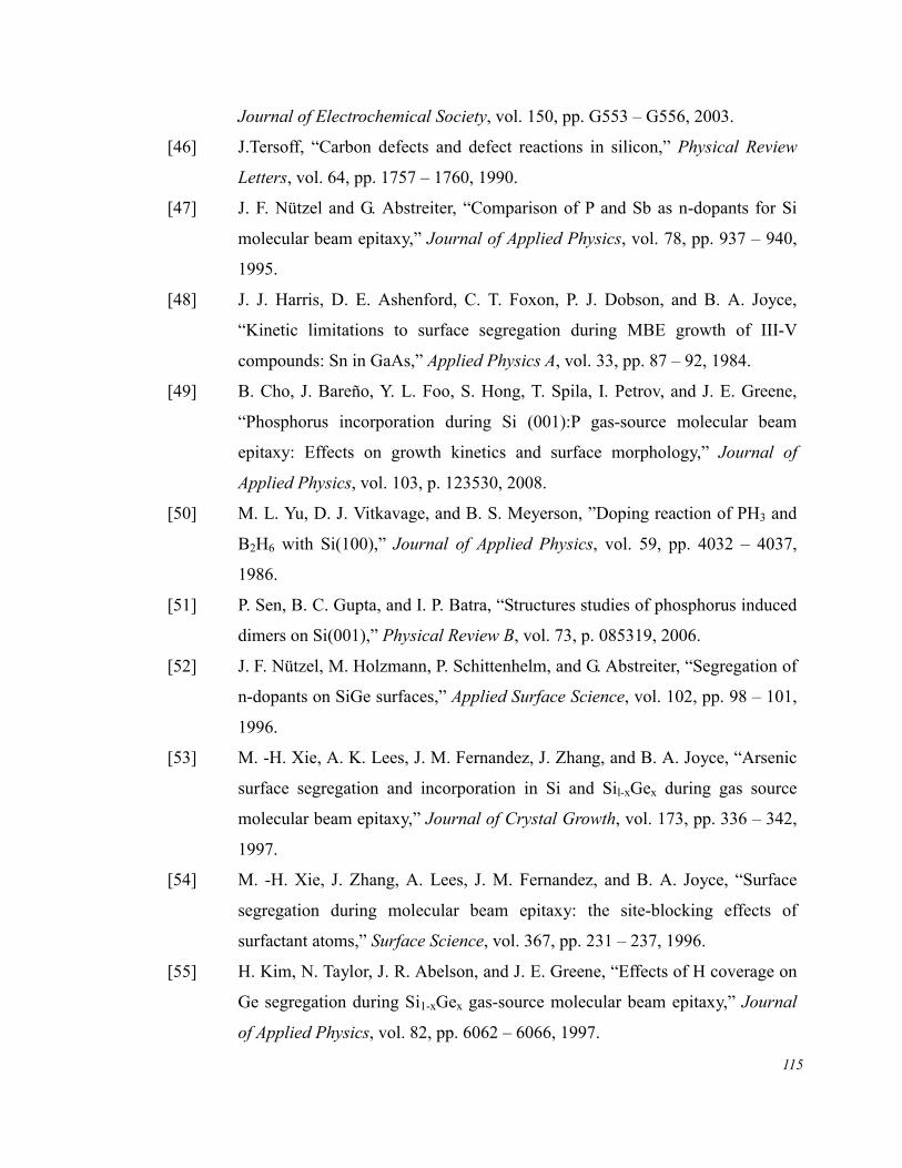
115
Journal of Electrochemical Society, vol. 150, pp. G553 – G556, 2003.
[46] J.Tersoff, “Carbon defects and defect reactions in silicon,” Physical Review
Letters, vol. 64, pp. 1757 – 1760, 1990.
[47] J. F. Nützel and G. Abstreiter, “Comparison of P and Sb as n-dopants for Si
molecular beam epitaxy,” Journal of Applied Physics, vol. 78, pp. 937 – 940,
1995.
[48] J. J. Harris, D. E. Ashenford, C. T. Foxon, P. J. Dobson, and B. A. Joyce,
“Kinetic limitations to surface segregation during MBE growth of III-V
compounds: Sn in GaAs,” Applied Physics A, vol. 33, pp. 87 – 92, 1984.
[49] B. Cho, J. Bareño, Y. L. Foo, S. Hong, T. Spila, I. Petrov, and J. E. Greene,
“Phosphorus incorporation during Si (001):P gas-source molecular beam
epitaxy: Effects on growth kinetics and surface morphology,” Journal of
Applied Physics, vol. 103, p. 123530, 2008.
[50] M. L. Yu, D. J. Vitkavage, and B. S. Meyerson, ”Doping reaction of PH3 and
B2H6 with Si(100),” Journal of Applied Physics, vol. 59, pp. 4032 – 4037,
1986.
[51] P. Sen, B. C. Gupta, and I. P. Batra, “Structures studies of phosphorus induced
dimers on Si(001),” Physical Review B, vol. 73, p. 085319, 2006.
[52] J. F. Nützel, M. Holzmann, P. Schittenhelm, and G. Abstreiter, “Segregation of
n-dopants on SiGe surfaces,” Applied Surface Science, vol. 102, pp. 98 – 101,
1996.
[53] M. -H. Xie, A. K. Lees, J. M. Fernandez, J. Zhang, and B. A. Joyce, “Arsenic
surface segregation and incorporation in Si and Sil-xGex during gas source
molecular beam epitaxy,” Journal of Crystal Growth, vol. 173, pp. 336 – 342,
1997.
[54] M. -H. Xie, J. Zhang, A. Lees, J. M. Fernandez, and B. A. Joyce, “Surface
segregation during molecular beam epitaxy: the site-blocking effects of
surfactant atoms,” Surface Science, vol. 367, pp. 231 – 237, 1996.
[55] H. Kim, N. Taylor, J. R. Abelson, and J. E. Greene, “Effects of H coverage on
Ge segregation during Si1-xGex gas-source molecular beam epitaxy,” Journal
of Applied Physics, vol. 82, pp. 6062 – 6066, 1997.
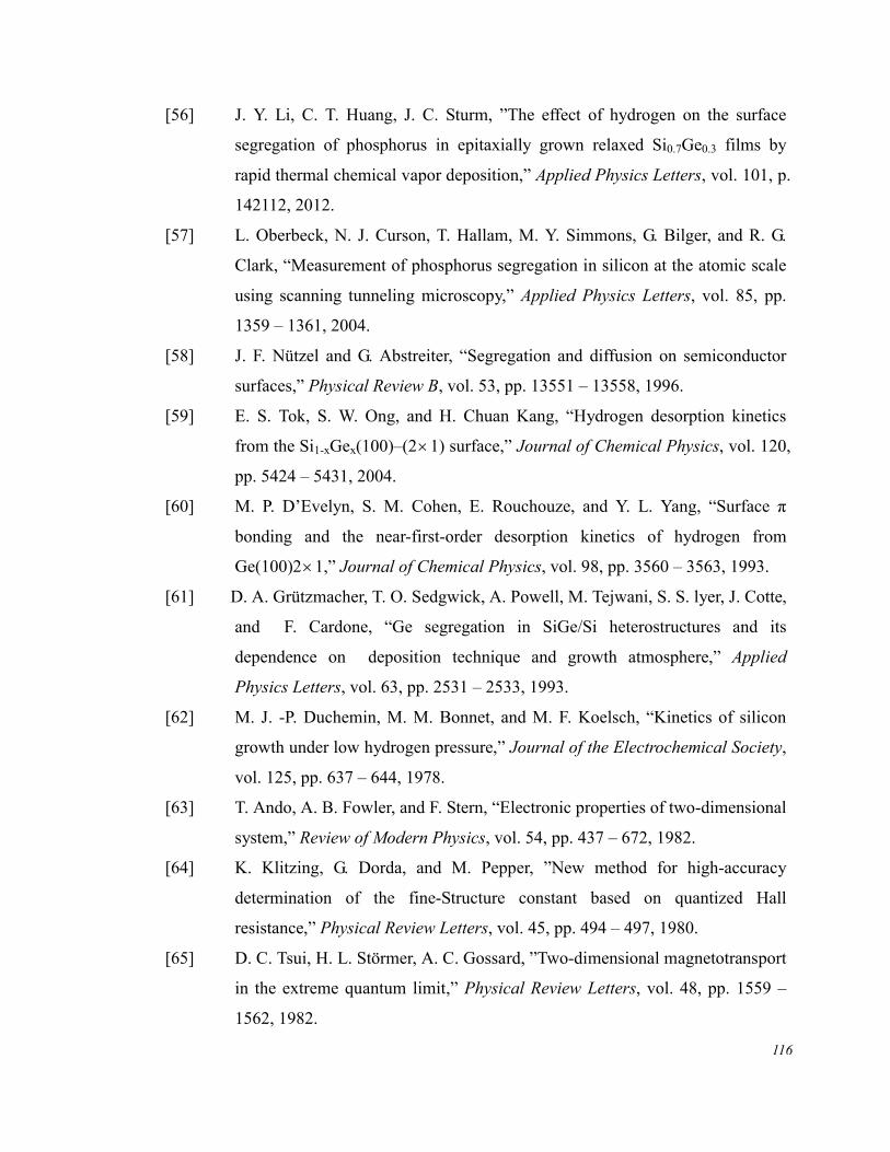
116
[56] J. Y. Li, C. T. Huang, J. C. Sturm, ”The effect of hydrogen on the surface
segregation of phosphorus in epitaxially grown relaxed Si0.7Ge0.3 films by
rapid thermal chemical vapor deposition,” Applied Physics Letters, vol. 101, p.
142112, 2012.
[57] L. Oberbeck, N. J. Curson, T. Hallam, M. Y. Simmons, G. Bilger, and R. G.
Clark, “Measurement of phosphorus segregation in silicon at the atomic scale
using scanning tunneling microscopy,” Applied Physics Letters, vol. 85, pp.
1359 – 1361, 2004.
[58] J. F. Nützel and G. Abstreiter, “Segregation and diffusion on semiconductor
surfaces,” Physical Review B, vol. 53, pp. 13551 – 13558, 1996.
[59] E. S. Tok, S. W. Ong, and H. Chuan Kang, “Hydrogen desorption kinetics
from the Si1-xGex(100)–(21) surface,” Journal of Chemical Physics, vol. 120,
pp. 5424 – 5431, 2004.
[60] M. P. D’Evelyn, S. M. Cohen, E. Rouchouze, and Y. L. Yang, “Surface π
bonding and the near-first-order desorption kinetics of hydrogen from
Ge(100)21,” Journal of Chemical Physics, vol. 98, pp. 3560 – 3563, 1993.
[61] D. A. Grützmacher, T. O. Sedgwick, A. Powell, M. Tejwani, S. S. lyer, J. Cotte,
and F. Cardone, “Ge segregation in SiGe/Si heterostructures and its
dependence on deposition technique and growth atmosphere,” Applied
Physics Letters, vol. 63, pp. 2531 – 2533, 1993.
[62] M. J. -P. Duchemin, M. M. Bonnet, and M. F. Koelsch, “Kinetics of silicon
growth under low hydrogen pressure,” Journal of the Electrochemical Society,
vol. 125, pp. 637 – 644, 1978.
[63] T. Ando, A. B. Fowler, and F. Stern, “Electronic properties of two-dimensional
system,” Review of Modern Physics, vol. 54, pp. 437 – 672, 1982.
[64] K. Klitzing, G. Dorda, and M. Pepper, ”New method for high-accuracy
determination of the fine-Structure constant based on quantized Hall
resistance,” Physical Review Letters, vol. 45, pp. 494 – 497, 1980.
[65] D. C. Tsui, H. L. Störmer, A. C. Gossard, ”Two-dimensional magnetotransport
in the extreme quantum limit,” Physical Review Letters, vol. 48, pp. 1559 –
1562, 1982.
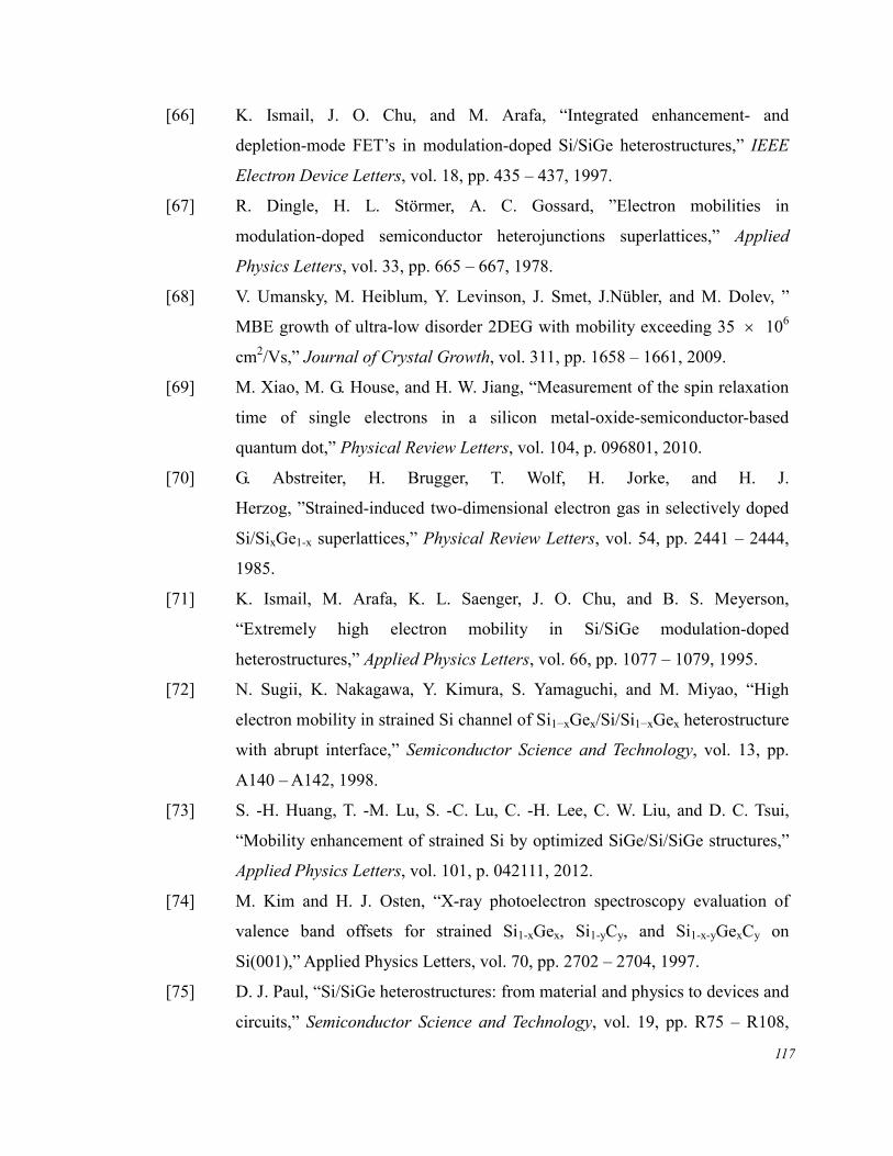
117
[66] K. Ismail, J. O. Chu, and M. Arafa, “Integrated enhancement- and
depletion-mode FET’s in modulation-doped Si/SiGe heterostructures,” IEEE
Electron Device Letters, vol. 18, pp. 435 – 437, 1997.
[67] R. Dingle, H. L. Störmer, A. C. Gossard, ”Electron mobilities in
modulation-doped semiconductor heterojunctions superlattices,” Applied
Physics Letters, vol. 33, pp. 665 – 667, 1978.
[68] V. Umansky, M. Heiblum, Y. Levinson, J. Smet, J.Nübler, and M. Dolev, ”
MBE growth of ultra-low disorder 2DEG with mobility exceeding 35 106
cm2/Vs,” Journal of Crystal Growth, vol. 311, pp. 1658 – 1661, 2009.
[69] M. Xiao, M. G. House, and H. W. Jiang, “Measurement of the spin relaxation
time of single electrons in a silicon metal-oxide-semiconductor-based
quantum dot,” Physical Review Letters, vol. 104, p. 096801, 2010.
[70] G. Abstreiter, H. Brugger, T. Wolf, H. Jorke, and H. J.
Herzog, ”Strained-induced two-dimensional electron gas in selectively doped
Si/SixGe1-x superlattices,” Physical Review Letters, vol. 54, pp. 2441 – 2444,
1985.
[71] K. Ismail, M. Arafa, K. L. Saenger, J. O. Chu, and B. S. Meyerson,
“Extremely high electron mobility in Si/SiGe modulation-doped
heterostructures,” Applied Physics Letters, vol. 66, pp. 1077 – 1079, 1995.
[72] N. Sugii, K. Nakagawa, Y. Kimura, S. Yamaguchi, and M. Miyao, “High
electron mobility in strained Si channel of Si1−xGex/Si/Si1−xGex heterostructure
with abrupt interface,” Semiconductor Science and Technology, vol. 13, pp.
A140 – A142, 1998.
[73] S. -H. Huang, T. -M. Lu, S. -C. Lu, C. -H. Lee, C. W. Liu, and D. C. Tsui,
“Mobility enhancement of strained Si by optimized SiGe/Si/SiGe structures,”
Applied Physics Letters, vol. 101, p. 042111, 2012.
[74] M. Kim and H. J. Osten, “X-ray photoelectron spectroscopy evaluation of
valence band offsets for strained Si1-xGex, Si1-yCy, and Si1-x-yGexCy on
Si(001),” Applied Physics Letters, vol. 70, pp. 2702 – 2704, 1997.
[75] D. J. Paul, “Si/SiGe heterostructures: from material and physics to devices and
circuits,” Semiconductor Science and Technology, vol. 19, pp. R75 – R108,
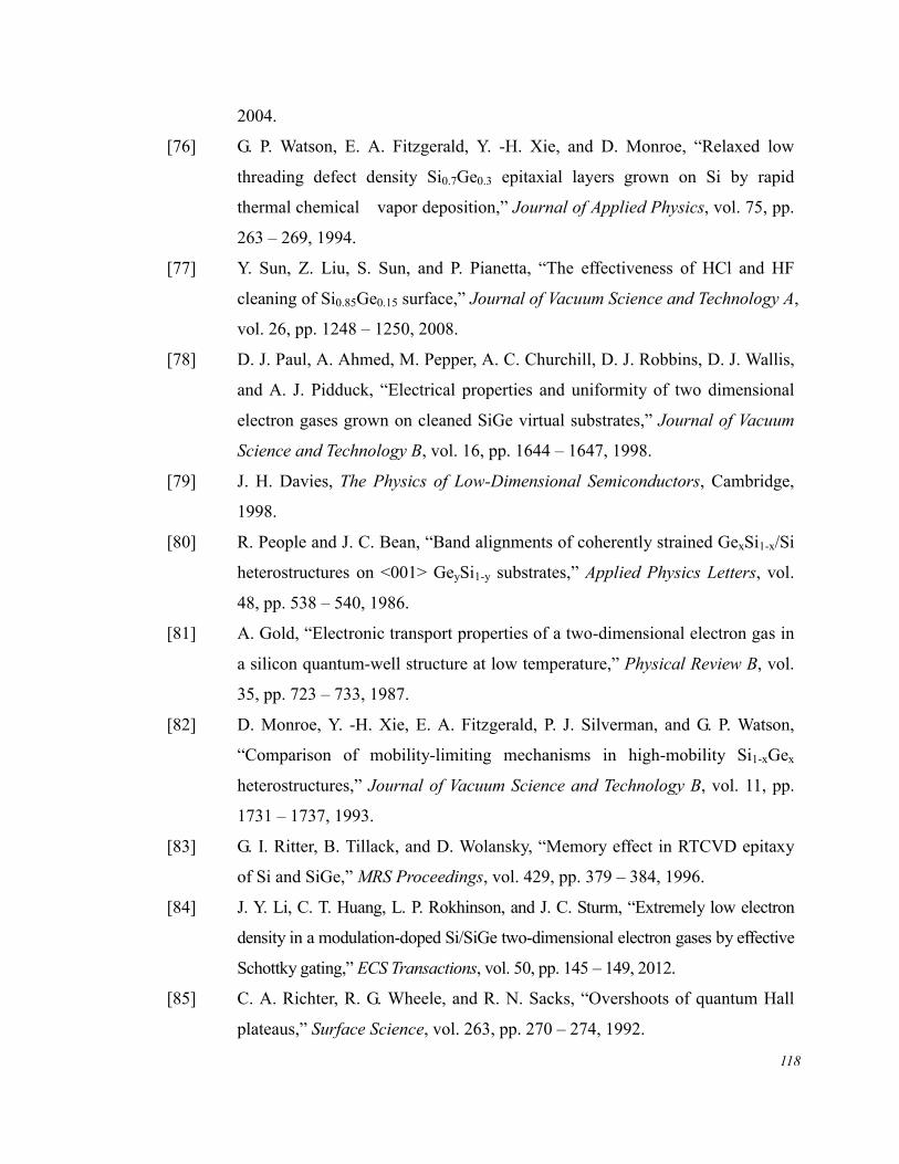
118
2004.
[76] G. P. Watson, E. A. Fitzgerald, Y. -H. Xie, and D. Monroe, “Relaxed low
threading defect density Si0.7Ge0.3 epitaxial layers grown on Si by rapid
thermal chemical vapor deposition,” Journal of Applied Physics, vol. 75, pp.
263 – 269, 1994.
[77] Y. Sun, Z. Liu, S. Sun, and P. Pianetta, “The effectiveness of HCl and HF
cleaning of Si0.85Ge0.15 surface,” Journal of Vacuum Science and Technology A,
vol. 26, pp. 1248 – 1250, 2008.
[78] D. J. Paul, A. Ahmed, M. Pepper, A. C. Churchill, D. J. Robbins, D. J. Wallis,
and A. J. Pidduck, “Electrical properties and uniformity of two dimensional
electron gases grown on cleaned SiGe virtual substrates,” Journal of Vacuum
Science and Technology B, vol. 16, pp. 1644 – 1647, 1998.
[79] J. H. Davies, The Physics of Low-Dimensional Semiconductors, Cambridge,
1998.
[80] R. People and J. C. Bean, “Band alignments of coherently strained GexSi1-x/Si
heterostructures on <001> GeySi1-y substrates,” Applied Physics Letters, vol.
48, pp. 538 – 540, 1986.
[81] A. Gold, “Electronic transport properties of a two-dimensional electron gas in
a silicon quantum-well structure at low temperature,” Physical Review B, vol.
35, pp. 723 – 733, 1987.
[82] D. Monroe, Y. -H. Xie, E. A. Fitzgerald, P. J. Silverman, and G. P. Watson,
“Comparison of mobility-limiting mechanisms in high-mobility Si1-xGex
heterostructures,” Journal of Vacuum Science and Technology B, vol. 11, pp.
1731 – 1737, 1993.
[83] G. I. Ritter, B. Tillack, and D. Wolansky, “Memory effect in RTCVD epitaxy
of Si and SiGe,” MRS Proceedings, vol. 429, pp. 379 – 384, 1996.
[84] J. Y. Li, C. T. Huang, L. P. Rokhinson, and J. C. Sturm, “Extremely low electron
density in a modulation-doped Si/SiGe two-dimensional electron gases by effective
Schottky gating,” ECS Transactions, vol. 50, pp. 145 – 149, 2012.
[85] C. A. Richter, R. G. Wheele, and R. N. Sacks, “Overshoots of quantum Hall
plateaus,” Surface Science, vol. 263, pp. 270 – 274, 1992.
119
[86] S. Komiyama, H. Nii, M. Ohsaw, S. Fukatsu, Y. Shiraki, R. Itoh, and H.
Toyoshima, “Resistance and resistivity of two dimensional electron gas at high
magnetic fields,” Solid State Communications, vol. 80, pp. 157 – 163, 1991.
[87] J. W. Matthews and A. E. Blakeslee, “Defects in epitaxial multilayers: I. Misfit
dislocations,” Journal of Crystal Growth, vol. 27, pp. 118 – 125, 1974.
[88] H. Sakaki, T. Noda, K. Hirakawa, M. Tanaka, and T. Matsusue, “Interface
roughness scattering in GaAsl/AlAs quantum wens,” Applied Physics Letters,
vol. 51, pp. 1934 – 1936, 1987.
[89] A. Gold, “Mobility and metal–insulator transition of the two-dimensional
electron gas in SiGe/Si/SiGe quantum wells,” Journal of Applied Physics, vol.
108, p. 063710, 2010.
[90] J. A. Nixon and J. H. Davies, “Potential fluctuations in heterostructure
devices,” Physical Review B, vol. 41, pp. 7929 – 7932, 1990.
[91] D. Laroche, S. Das Sarma, G. Gervais, M. P. Lilly, and J. L. Reno, “Scattering
mechanism in modulated-doped shallow two-dimensional electron gas,”
Applied Physics Letters, vol. 96, p. 162112, 2010.
[92] Z. Wilamowski, N. Sandersfeld, W. Jantsch, D. Többen, and F. Schäffler,
“Screening breakdown on the route toward the metal-insulator transition in
modulation-doped Si/SiGe quantum wells,” Physical Review Letters, vol. 87,
p. 026401, 2001.
[93] E. F. Schubert, K. Ploog, H. Dämbkes, and K. Heime, “Selectively doped
n-AlxGa1-xAs/GaAs heterostructures with high-mobility two-dimensional electron
gas for field effect transistors,”Applied Physics A, vol. 33, pp. 63 – 76, 1984.
[94] M. A. Reed, W. P. Kirk, and P. S. Kobiela, “Investigating of parallel
conduction in GaAs/AlxGa1-xAs modulation-doped structures in the quantum
limit,” IEEE Journal of Quantum Electronics, vol. 22, pp. 1753 – 1759, 1986.
[95] K. Ensslin, D. Heitmann, R. R. Gerhardts, and K. Ploog, “Population process
of the upper subband in AlxGa1-xAs-GaAs quantum wells,” Physical Review B,
vol. 39, pp. 12993 – 12996, 1989.
[96] T. M. Lu, C. -H. Lee, S. -H. Huang, D. C. Tsui, and C. W. Liu, “Upper limit of
two-dimensional electron density in enhancement-mode Si/SiGe
120
heterostructure field-effect transistors,” Applied Physics Letters, vol. 99, p.
153510, 2011.
[97] D. R. Lide, CRC Handbook of Chemistry and Physics, CRC Press, 2006.
[98] A. Wild, J. Kierig, J. Sailer, J. W. Ager III, E. E. Haller, G. Abstreiter, S.
Ludwig, and D. Bougeard, “Few electron double quantum dot in an
isotopically purified 28Si quantum well,” Applied Physics Letters, vol. 100, p.
143110, 2012.
[99] L. V. C. Assali, H. M. Petrilli, R. B. Capaz, B. Koiller, X. Hu, and S. Das
Sarma, “Hyperfine interactions in silicon quantum dots,” Physical Review B,
vol. 83, p. 165301, 2011.
[100] K. Yao, Silicon and Silicon-Germanium Epitaxy for Quantum Dot Device
Fabrications towards an Electron Spin-Based Quantum Computer, Ph.D.
dissertation, Princeton University, 2009.
[101] M. Kellogg, J. P. Eisenstein, L. N. Pfeiffer, and K. W. West, “Vanishing Hall
resistance at high magnetic field in a double-layer two-dimensional electron
system,” Physical Review Letters, vol. 93, p. 036801, 2004.
[102] D.J. Paul, A. Ahmed, A.C. Churchill, D.J. Robbins, and W.Y. Leong,
“Low-dimensional inverted Si/SiGe modulation-doped electron gases using
selective ex-situ ion implantation,” Materials Science and Engineering B, vol.
89, pp. 111 – 115, 2002.
[103] H. L. Störmer, A. C. Gossard, and W. Wiegmann, “Observation of
intersubband scattering in a 2-dimensional electron system,” Solid State
Communications, vol. 41, pp. 707 – 709, 1982.
[104] T. P. Smith III and F. F. Fang, “Upper-subband transport in GaAs
heterostructures,” Physical Review B, vol. 37, pp. 4303 – 4305, 1988.
[105] R. Fletcher, E. Zaremba, M. D’Iorio, C. T. Foxon, and J. J. Haris, “Evidence
of a mobility edge in the second subband of an Al0.33Ga0.67As-GaAs
heterojunctions,” Physical Review B, vol. 38, pp. 7866 – 7869, 1988.
[106] C. Jiang, D. C. Tsui, and G. Weimann, “Threshold transport of high-mobility
two-dimensional electron gas in GaAs/AlGaAs heterostructures,” Applied
Physics Letters, vol. 53, pp. 1533 – 1535, 1988.
121
Appendix: Publications and Conference
Presentations Resulting from this Thesis
Journal Articles
[1] Jiun-Yun Li, C. T. Huang, L. P. Rokhinson, and J. C. Sturm, “Extremely high
electron mobility in an inverted modulation-doped Si two-dimensional
electron gas by a sharp turn-off of phosphorus,” manuscript in preparation.
[2] Jiun-Yun Li, C. T. Huang, L. P. Rokhinson, and J. C. Sturm, “Extremely high
electron mobility in isotopically enriched 28Si quantum wells grown by
chemical vapor deposition,” manuscript to be submitted to Applied Physics
Letters.
[3] Jiun-Yun Li and J. C. Sturm, “The effects of germanium fraction on high-field
band-to-band tunneling in p+-SiGe/n+-SiGe junctions in forward and reverse
biases,” accepted for publication in IEEE Transactions on Electron Devices.
[4] C. T. Huang, Jiun-Yun Li, and J. C. Sturm, “Implant isolation of silicon
two-dimensional electron gases at 4.2 K,” IEEE Electron Device Letters, vol.
34, pp. 21 – 23, 2013.
[5] Jiun-Yun Li, C. T. Huang, L. P. Rokhinson, and J. C. Sturm, “Extremely low
electron density in a modulation-doped Si/SiGe two-dimensional electron gas
by effective Schottky gating,” ECS Transactions, vol. 50, pp. 145 – 149, 2012.
[6] Jiun-Yun Li, C. T. Huang, J. C. Sturm, ”The effect of hydrogen on the surface
segregation of phosphorus in epitaxially grown relaxed Si0.7Ge0.3 films by
rapid thermal chemical vapor deposition,” Applied Physics Letters, vol. 101, p.
142112, 2012.
122
Conference Presentations
[1] C. T. Huang, Jiun-Yun Li, and J. C. Sturm, “Very low electron density in
undoped enhancement-mode Si/SiGe two-dimensional electron gases with
thin SiGe cap layers,” 223rd Meeting of the Electrochemical Society, Toronto,
ON, Canada, May. 12 – 17, 2013.
[2] Jiun-Yun Li, C. T. Huang, L. P. Rokhinson, and J. C. Sturm, “Extremely low
electron density in a modulation-doped Si/SiGe 2DEG by effective Schottky
gating,” 222nd Meeting of the Electrochemical Society, Honolulu, HI, Oct. 7 –
12, 2012.
[3] Jiun-Yun Li, C. T. Huang, and J. C. Sturm, “Extremely sharp phosphorus
turn-off slope and effect of hydrogen on phosphorus surface segregation in
epitaxially-grown relaxed Si0.7Ge0.3 by RTCVD,” International SiGe
Technology and Device Meeting, Berkeley, CA, June 4 – 6, 2012.
[4] C. T. Huang, Jiun-Yun Li, and J. C. Sturm, “High breakdown voltage
Schottky gating of doped Si/SiGe 2DEG system enabled by suppression of
phosphorus surface segregation,” International SiGe Technology and Device
Meeting, Berkeley, CA, June 4 – 6, 2012.
[5] Jiun-Yun Li, C. T. Huang, L. Rokhinson, J. A. Ohlhausen, M. S. Carroll, and J.
C. Sturm, “High quality two-dimensional electron gases (2DEGs) in
isotopically-enriched strained Si,” 2012 APS March Meeting Session X29,
Boston, MA, Feb. 27 – Mar. 2, 2012.
[6] Jiun-Yun Li, K. S. Chou, C. T. Huang, J. C. Sturm, and L. P. Rokhinson,
“High quality two-dimensional electron gases (2DEGs) in modulation-doped
and enhancement-mode Si/SiGe heterostructures,” 2011 PCCM Symposium:
Quantum Control of Solid State Systems, Princeton, NJ, Nov. 3 – 5, 2011.
[7] Jiun-Yun Li, C. T. Huang, J. C. Sturm, and L. P. Rokhinson, “High quality
two-dimensional electron system (2DES) in n-Type Si/SiGe modulation-doped
heterostructures grown by RTCVD,” 2011 International Workshop on Silicon
Quantum Electronics, Denver, CO, August 14 ~ 15, 2011.
123
[8] K. Chou, Jiun-Yun Li, C. T. Huang, J. C. Sturm, and C. W. Liu, “Stable high
quality accumulation-mode Si 2DEG with a shallow top SiGe barrier of ~
25nm,” 2011 International Workshop on Silicon Quantum Electronics, Denver,
CO, August 14 ~ 15, 2011.
[9] Jiun-Yun Li, J. C. Sturm, I. Lauer, and S. Koester, “Effect of interface defects
and record high peak tunnel current density in Si-based tunnel diodes grown
by RTCVD,” 2011 MRS Spring Meeting, Symposium P7.11, San Francisco,
CA, April 25 – 29, 2011.
[10] Jiun-Yun Li, J. C. Sturm, A. Majumdar, I. Lauer, and S. Koester, “Bandgap
dependence of band-to-band tunneling and defect-mediated excess currents in
SiGe/Si heterojunction tunnel diodes grown by RTCVD,” 67th Annual Device
Research Conference (DRC 2009) Digest, pp. 99 – 100, University Park, PA,
June 22 ~ 24, 2009.