Embed Size (px)
DESCRIPTION
notes
Citation preview
EE 202 : DIGITAL ELECTRONICS 1
Chapter 4:
FLIP FLOPS (Sequential Circuits)
1
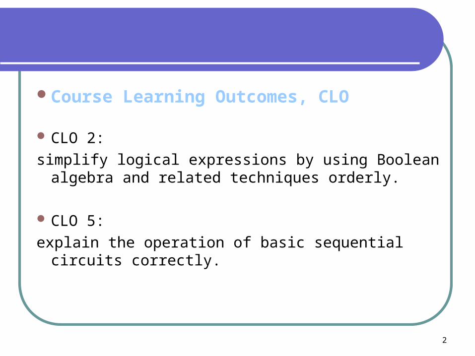
Course Learning Outcomes, CLO
CLO 2:
simplify logical expressions by using Boolean algebra and related techniques orderly.
CLO 5:
explain the operation of basic sequential circuits correctly.
2
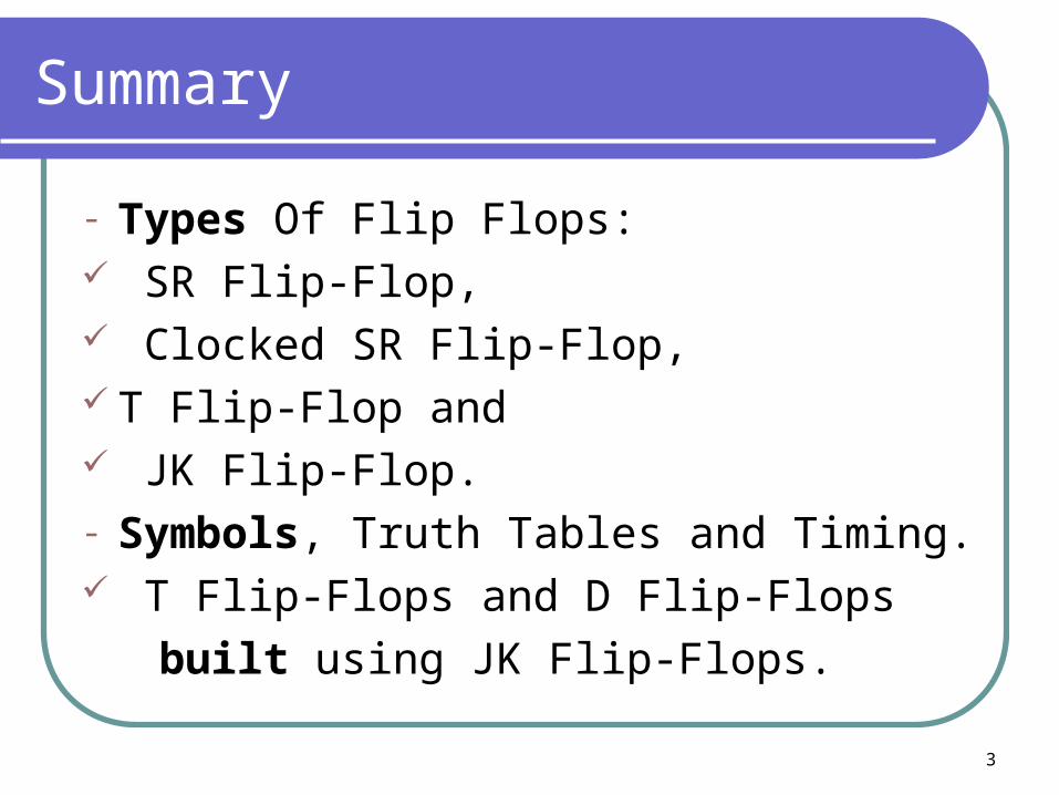
Summary
- Types Of Flip Flops: SR Flip-Flop, Clocked SR Flip-Flop, T Flip-Flop and JK Flip-Flop.- Symbols, Truth Tables and Timing. T Flip-Flops and D Flip-Flops
built using JK Flip-Flops.
3
4
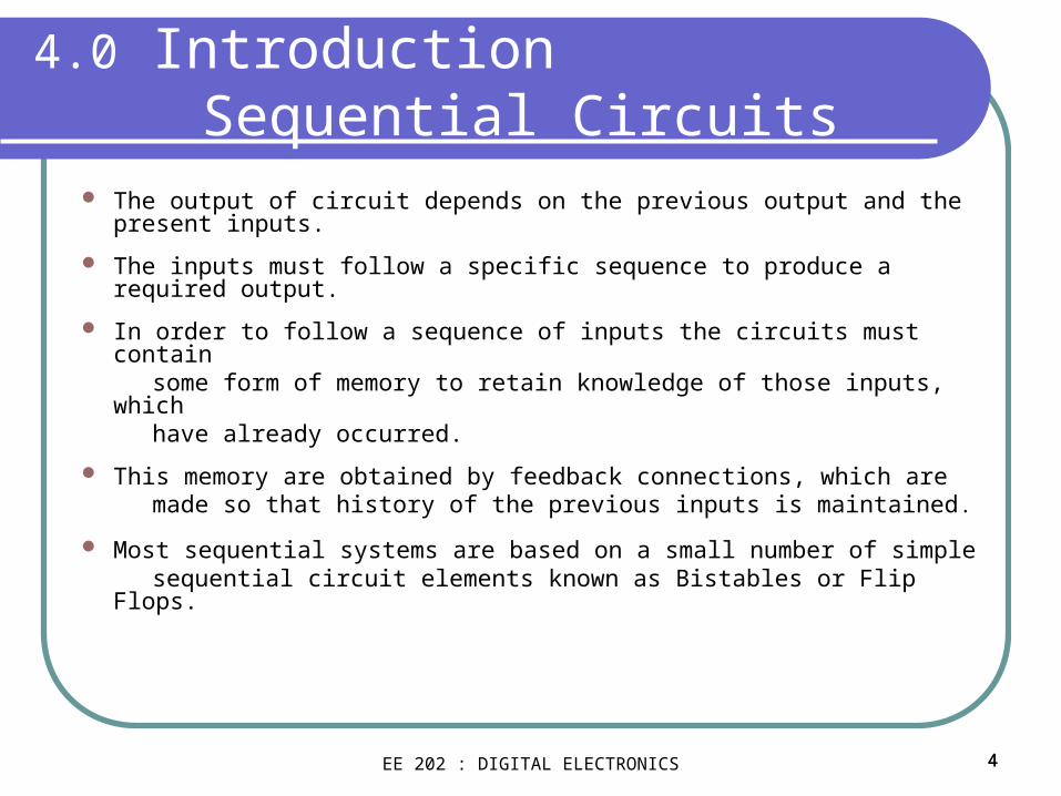
4.0 Introduction Sequential Circuits
The output of circuit depends on the previous output and the present inputs.
The inputs must follow a specific sequence to produce a required output.
In order to follow a sequence of inputs the circuits must contain some form of memory to retain knowledge of those inputs, which have already occurred.
This memory are obtained by feedback connections, which are made so that history of the previous inputs is maintained.
Most sequential systems are based on a small number of simple sequential circuit elements known as Bistables or Flip Flops.
EE 202 : DIGITAL ELECTRONICS 4
5
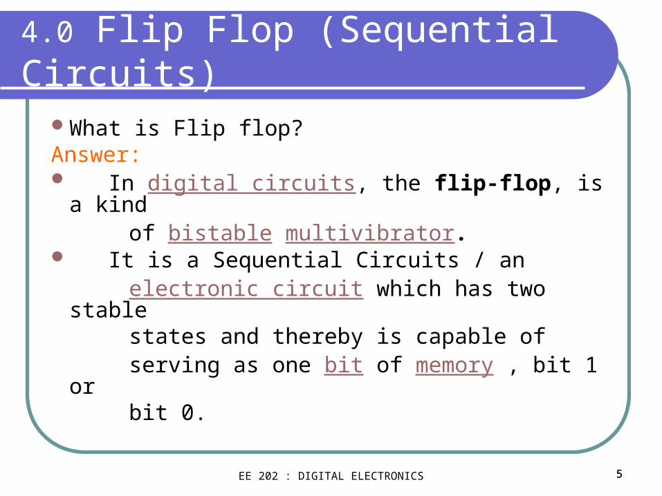
4.0 Flip Flop (Sequential Circuits)
What is Flip flop?Answer: In digital circuits, the flip-flop, is a kind of bistable multivibrator. It is a Sequential Circuits / an electronic circuit which has two stable states and thereby is capable of serving as one bit of memory , bit 1 or bit 0.
EE 202 : DIGITAL ELECTRONICS 5
6
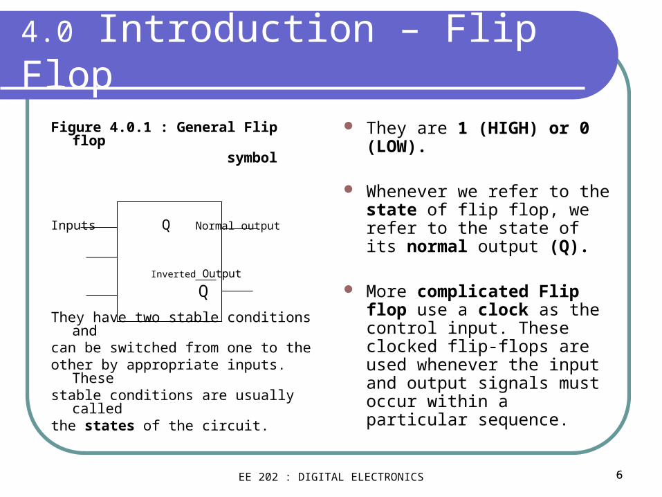
4.0 Introduction – Flip Flop
They are 1 (HIGH) or 0 (LOW).
Whenever we refer to the state of flip flop, we refer to the state of its normal output (Q).
More complicated Flip flop use a clock as the control input. These clocked flip-flops are used whenever the input and output signals must occur within a particular sequence.
Figure 4.0.1 : General Flip flop symbol
Inputs Q Normal output
Inverted Output
They have two stable conditions and can be switched from one to the other by appropriate inputs. These stable conditions are usually called the states of the circuit.
Q
EE 202 : DIGITAL ELECTRONICS 6
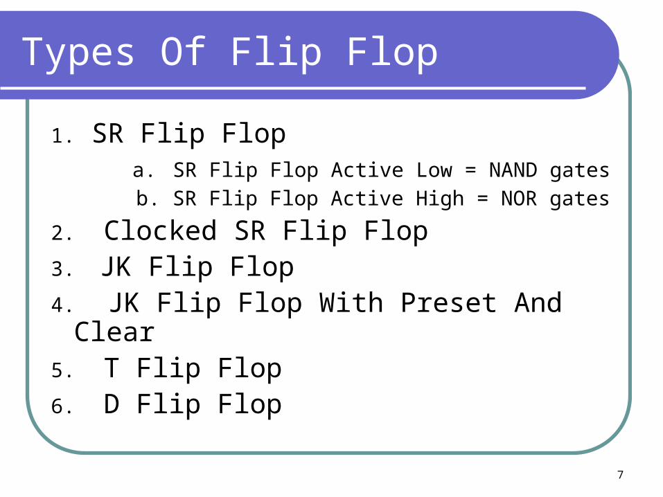
Types Of Flip Flop
1. SR Flip Flop a. SR Flip Flop Active Low = NAND gates b. SR Flip Flop Active High = NOR gates
2. Clocked SR Flip Flop3. JK Flip Flop4. JK Flip Flop With Preset And Clear5. T Flip Flop6. D Flip Flop
7
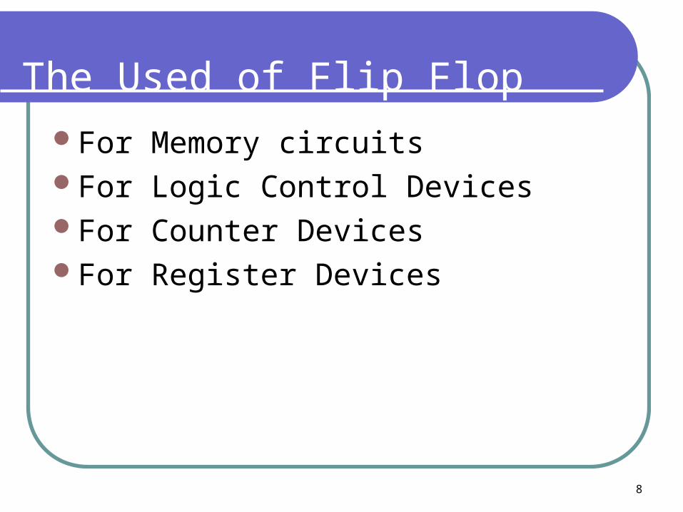
The Used of Flip Flop
For Memory circuitsFor Logic Control DevicesFor Counter DevicesFor Register Devices
8
9
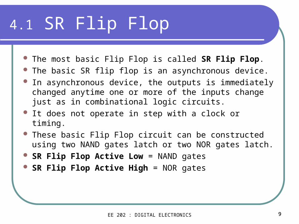
4.1 SR Flip Flop
The most basic Flip Flop is called SR Flip Flop. The basic SR flip flop is an asynchronous device. In asynchronous device, the outputs is immediately
changed anytime one or more of the inputs change just as in combinational logic circuits.
It does not operate in step with a clock or timing. These basic Flip Flop circuit can be constructed using
two NAND gates latch or two NOR gates latch. SR Flip Flop Active Low = NAND gates SR Flip Flop Active High = NOR gates
EE 202 : DIGITAL ELECTRONICS 9
10
4.1 SR Flip Flop
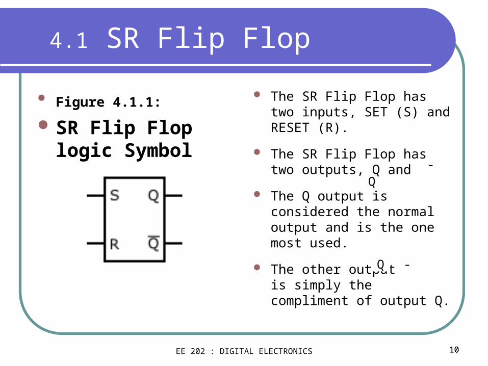
Figure 4.1.1: SR Flip Flop logic
Symbol
The SR Flip Flop has two inputs, SET (S) and RESET (R).
The SR Flip Flop has two outputs, Q and ¯
The Q output is considered the normal output and is the one most used.
The other output ¯ is simply the compliment of output Q.
Q
Q
EE 202 : DIGITAL ELECTRONICS 10
11
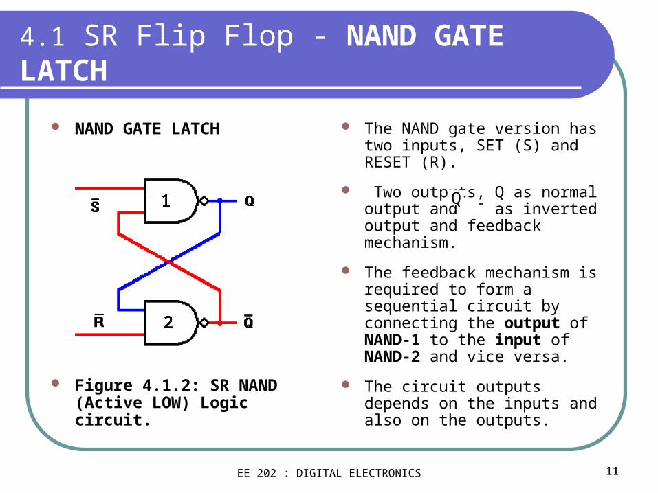
4.1 SR Flip Flop - NAND GATE LATCH
NAND GATE LATCH
Figure 4.1.2: SR NAND (Active LOW) Logic circuit.
The NAND gate version has two inputs, SET (S) and RESET (R).
Two outputs, Q as normal output and ¯ as inverted output and feedback mechanism.
The feedback mechanism is required to form a sequential circuit by connecting the output of NAND-1 to the input of NAND-2 and vice versa.
The circuit outputs depends on the inputs and also on the outputs.
Q1
2
1
2
1
2
1
2
1
2
1
2
1
2
1
2
1
2
1
2
1
2
1
2
EE 202 : DIGITAL ELECTRONICS 11
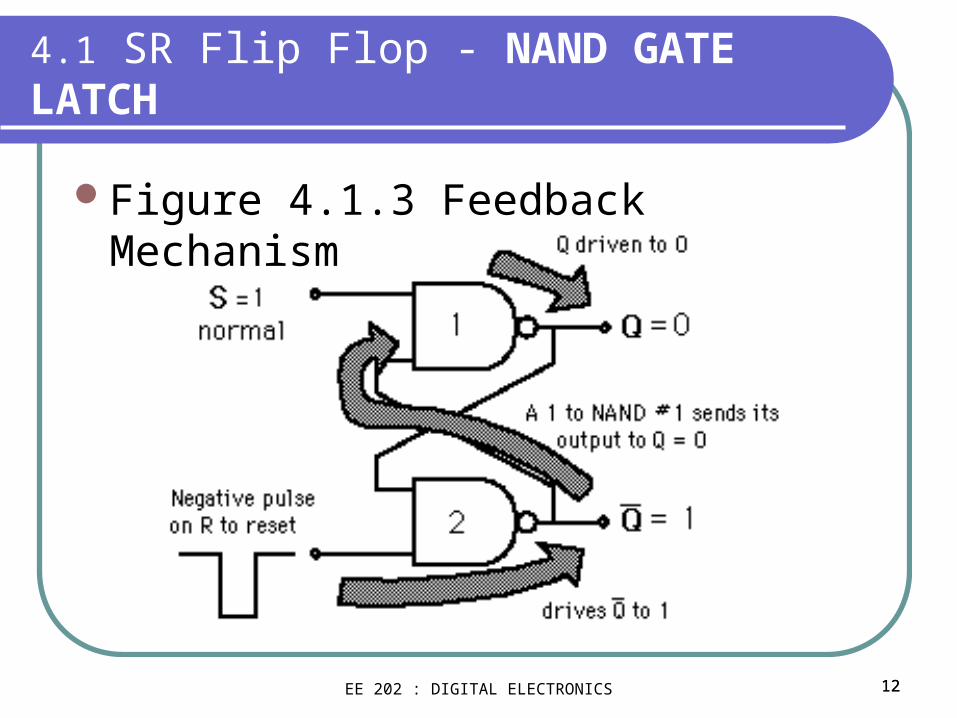
12
4.1 SR Flip Flop - NAND GATE LATCH
Figure 4.1.3 Feedback Mechanism
EE 202 : DIGITAL ELECTRONICS 12
13
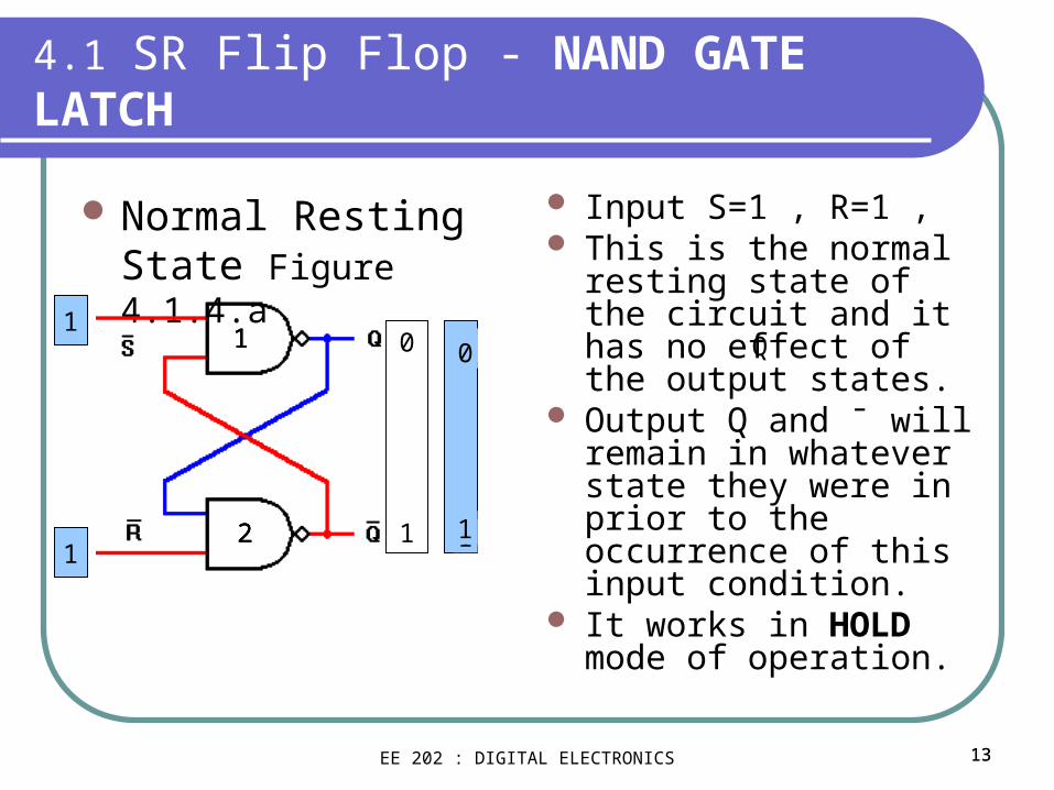
4.1 SR Flip Flop - NAND GATE LATCH
Normal Resting State Figure 4.1.4.a
Input S=1 , R=1 , This is the normal
resting state of the circuit and it has no effect of the output states.
Output Q and ¯ will remain in whatever state they were in prior to the occurrence of this input condition.
It works in HOLD mode of operation.
1
2
0
1
1
1
0
1
1
1
1
1
111
21
000
1
Q1
2
EE 202 : DIGITAL ELECTRONICS 13
14
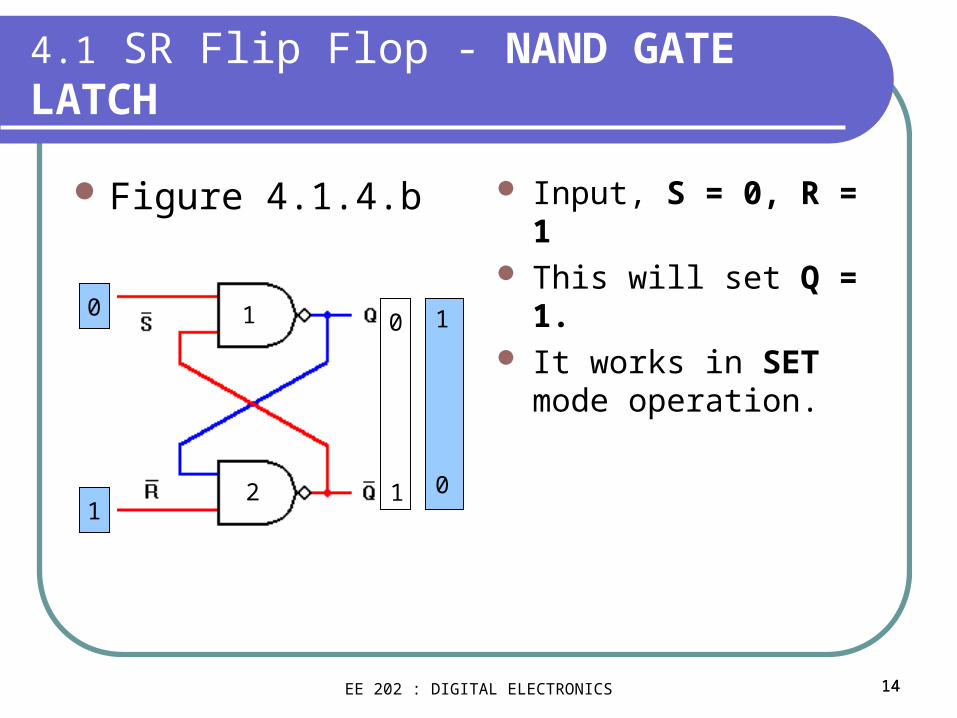
4.1 SR Flip Flop - NAND GATE LATCH
Input, S = 0, R = 1 This will set Q = 1. It works in SET mode
operation.
Figure 4.1.4.b
1
2
0
1
0 1
01
EE 202 : DIGITAL ELECTRONICS 14
15
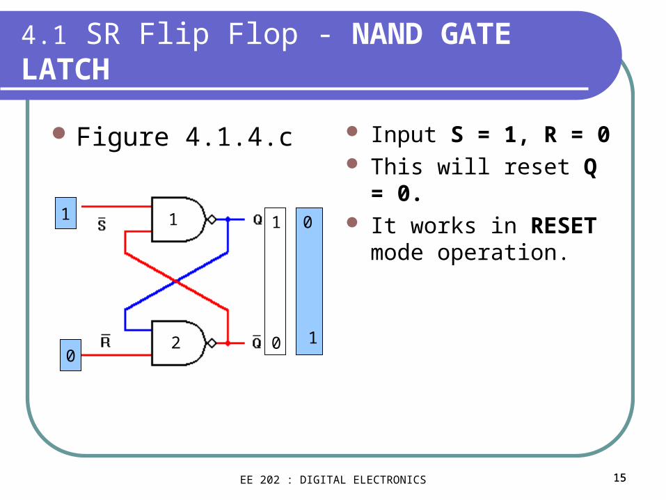
4.1 SR Flip Flop - NAND GATE LATCH
Figure 4.1.4.c Input S = 1, R = 0 This will reset Q = 0. It works in RESET mode
operation.1
2
1
01
0
0
1
EE 202 : DIGITAL ELECTRONICS 15
16
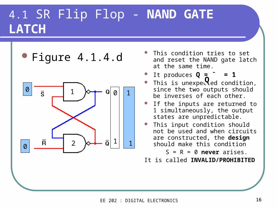
4.1 SR Flip Flop - NAND GATE LATCH
Figure 4.1.4.d This condition tries to set and
reset the NAND gate latch at the same time.
It produces Q = ¯ = 1 This is unexpected condition,
since the two outputs should be inverses of each other.
If the inputs are returned to 1 simultaneously, the output states are unpredictable.
This input condition should not be used and when circuits are constructed, the design should make this condition
S = R = 0 never arises.It is called INVALID/PROHIBITED
1
2
0
0 1
1
1
0
Q
EE 202 : DIGITAL ELECTRONICS 16
17
4.1 SR Flip Flop - NAND GATE LATCH
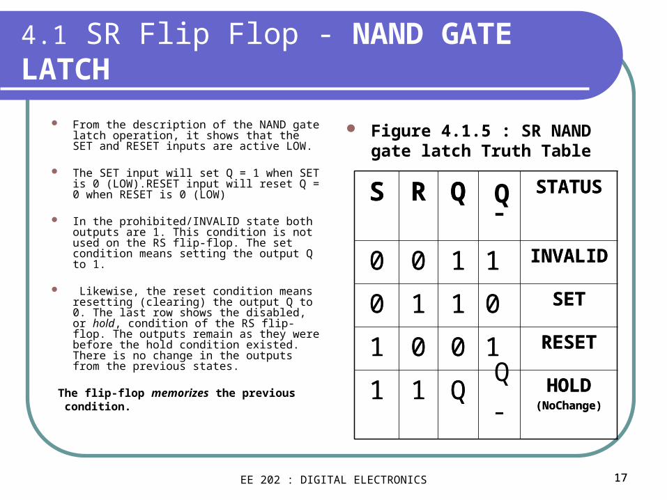
From the description of the NAND gate latch operation, it shows that the SET and RESET inputs are active LOW.
The SET input will set Q = 1 when SET is 0 (LOW).RESET input will reset Q = 0 when RESET is 0 (LOW)
In the prohibited/INVALID state both outputs are 1. This condition is not used on the RS flip-flop. The set condition means setting the output Q to 1.
Likewise, the reset condition means resetting (clearing) the output Q to 0. The last row shows the disabled, or hold, condition of the RS flip-flop. The outputs remain as they were before the hold condition existed. There is no change in the outputs from the previous states.
The flip-flop memorizes the previous condition.
Figure 4.1.5 : SR NAND gate latch Truth Table
S R Q ¯ STATUS
0 0 1 1 INVALID
0 1 1 0 SET
1 0 0 1 RESET
1 1 Q ¯ HOLD(NoChange)
Q
Q
S R Q ¯ STATUS
0 0 1 1 INVALID
0 1 1 0 SET
1 0 0 1 RESET
1 1 Q ¯ HOLD(NoChange)
EE 202 : DIGITAL ELECTRONICS 17
18
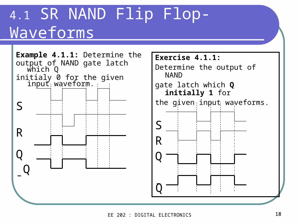
4.1 SR NAND Flip Flop-Waveforms
Exercise 4.1.1:Determine the output of NAND gate latch which Q initially 1 for the given input waveforms.
SRQ
¯
Example 4.1.1: Determine the output of NAND gate latch which Q initialy 0 for the given input waveform.
S
R
Q
¯Q
Q
EE 202 : DIGITAL ELECTRONICS 18
19
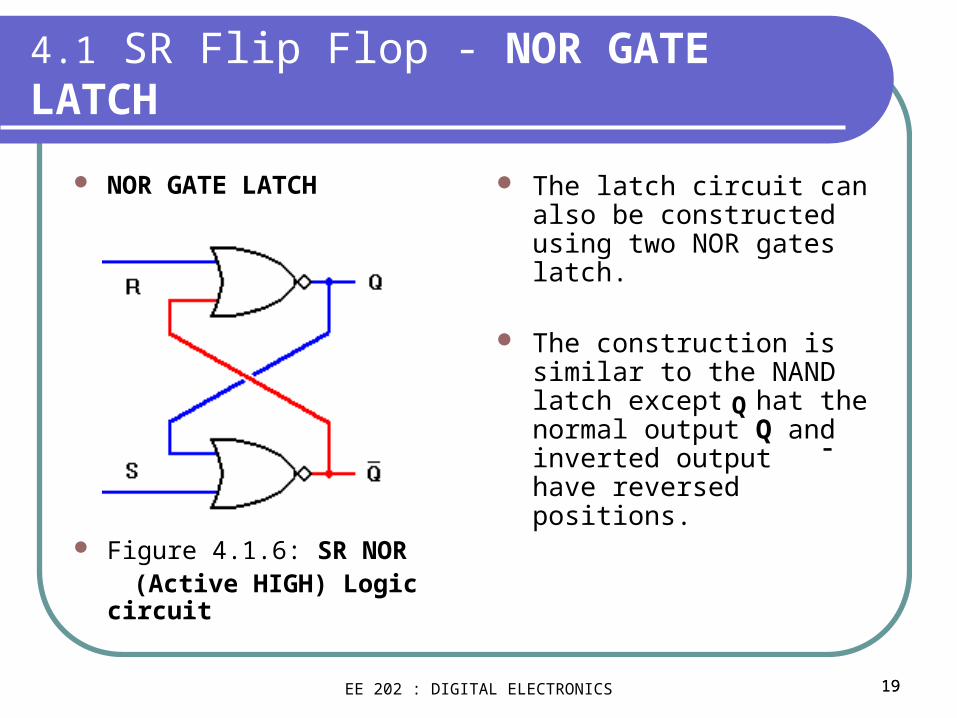
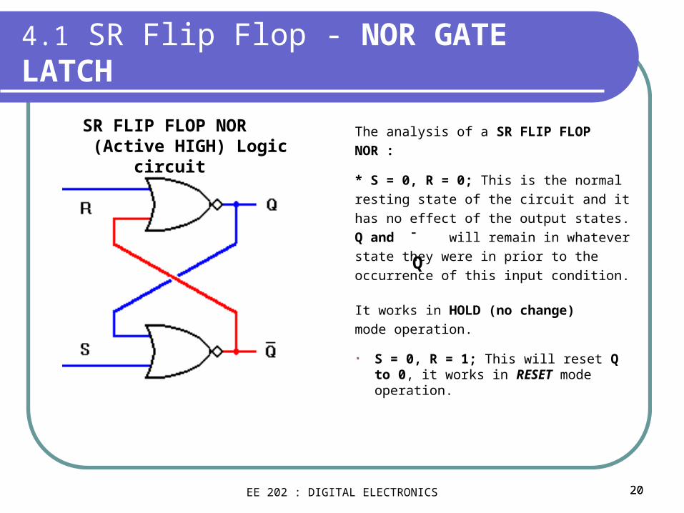
4.1 SR Flip Flop - NOR GATE LATCH
NOR GATE LATCH
Figure 4.1.6: SR NOR (Active HIGH) Logic circuit
The latch circuit can also be constructed using two NOR gates latch.
The construction is similar to the NAND latch except that the normal output Q and inverted output ¯ have reversed positions.
Q
EE 202 : DIGITAL ELECTRONICS 19
20
4.1 SR Flip Flop - NOR GATE LATCH
The analysis of a SR FLIP FLOP
NOR :
* S = 0, R = 0; This is the normal
resting state of the circuit and it
has no effect of the output states.
Q and ¯ will remain in whatever
state they were in prior to the
occurrence of this input condition.
It works in HOLD (no change)
mode operation.
• S = 0, R = 1; This will reset Q to 0, it works in RESET mode operation.
SR FLIP FLOP NOR (Active HIGH) Logic circuit
Q
EE 202 : DIGITAL ELECTRONICS 20
21
4.1 SR Flip Flop - NOR GATE LATCH
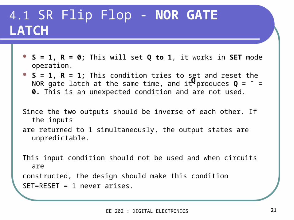
S = 1, R = 0; This will set Q to 1, it works in SET mode operation. S = 1, R = 1; This condition tries to set and reset the NOR gate
latch at the same time, and it produces Q = ¯ = 0. This is an unexpected condition and are not used.
Since the two outputs should be inverse of each other. If the inputs
are returned to 1 simultaneously, the output states are unpredictable.
This input condition should not be used and when circuits are
constructed, the design should make this condition
SET=RESET = 1 never arises.
Q
EE 202 : DIGITAL ELECTRONICS 21
22
4.1 SR Flip Flop - NOR GATE LATCH
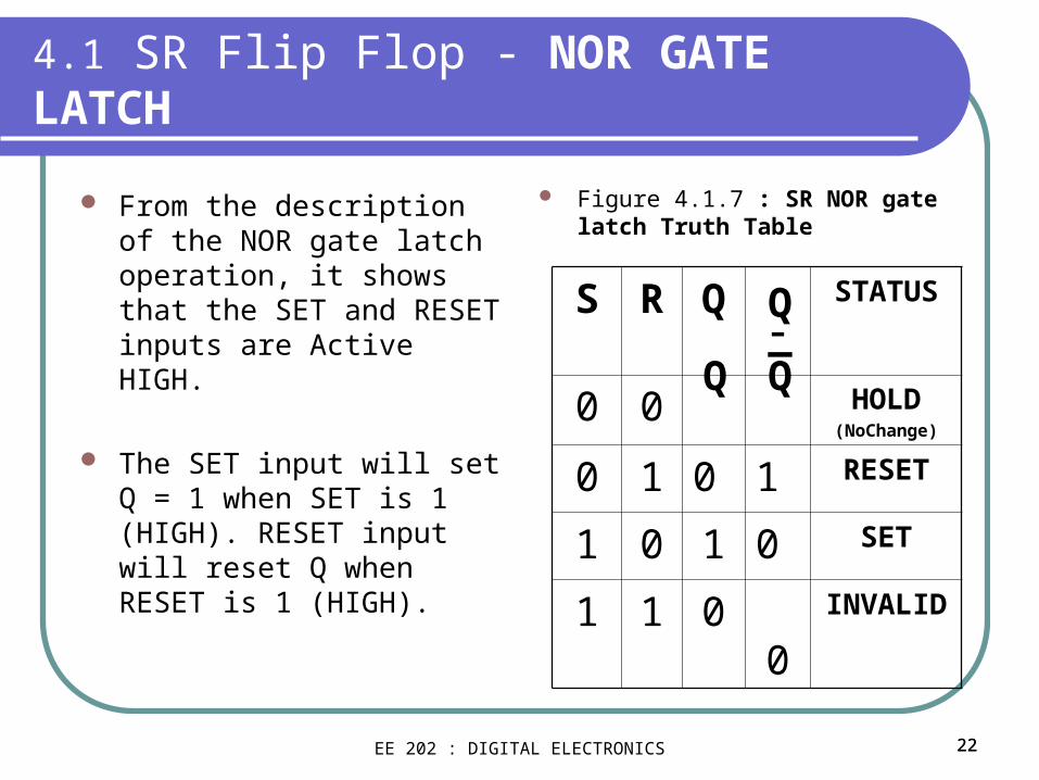
From the description of the NOR gate latch operation, it shows that the SET and RESET inputs are Active HIGH.
The SET input will set Q = 1 when SET is 1 (HIGH). RESET input will reset Q when RESET is 1 (HIGH).
Figure 4.1.7 : SR NOR gate latch Truth Table
S R Q ¯ STATUS
0 0 HOLD(NoChange)
0 1 0 1 RESET
1 0 1 0 SET
1 1 0 0 INVALID
Q Q
Q_
EE 202 : DIGITAL ELECTRONICS 22
23
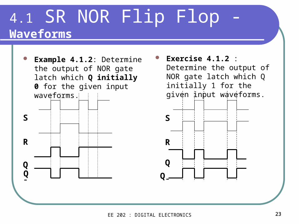
4.1 SR NOR Flip Flop -Waveforms
Example 4.1.2: Determine the output of NOR gate latch which Q initially 0 for the given input waveforms.
S
R
Q
¯
Exercise 4.1.2 : Determine the output of NOR gate latch which Q initially 1 for the given input waveforms.
S
R
Q
¯Q Q
EE 202 : DIGITAL ELECTRONICS 23
24
4.2 The CLOCK
In synchronous device, the exact times at which any output can change states are controlled by a signal commonly called the clock.
The clock signal is generally a rectangular pulse train or a square wave as shown in figure 4.9.
The clock is distributed to all parts of the system, and most of the system outputs can change state only when the clock makes a transition.
EE 202 : DIGITAL ELECTRONICS 24
25
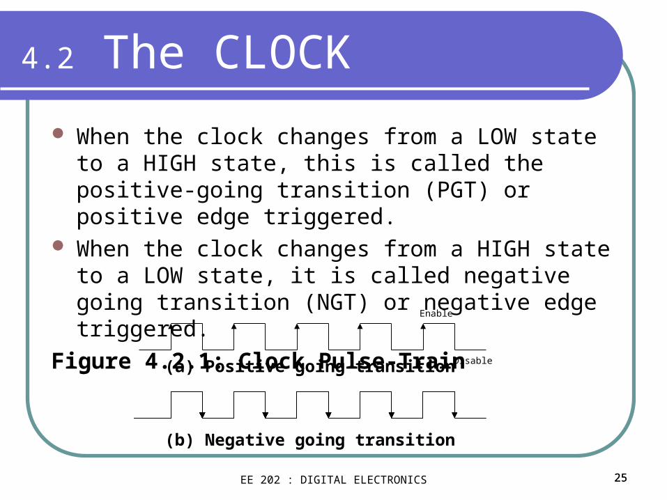
4.2 The CLOCK
When the clock changes from a LOW state to a HIGH state, this is called the positive-going transition (PGT) or positive edge triggered.
When the clock changes from a HIGH state to a LOW state, it is called negative going transition (NGT) or negative edge triggered.
Figure 4.2.1: Clock Pulse-Train
(a) Positive going transition
(b) Negative going transition
Enable
Disable
EE 202 : DIGITAL ELECTRONICS 25
26
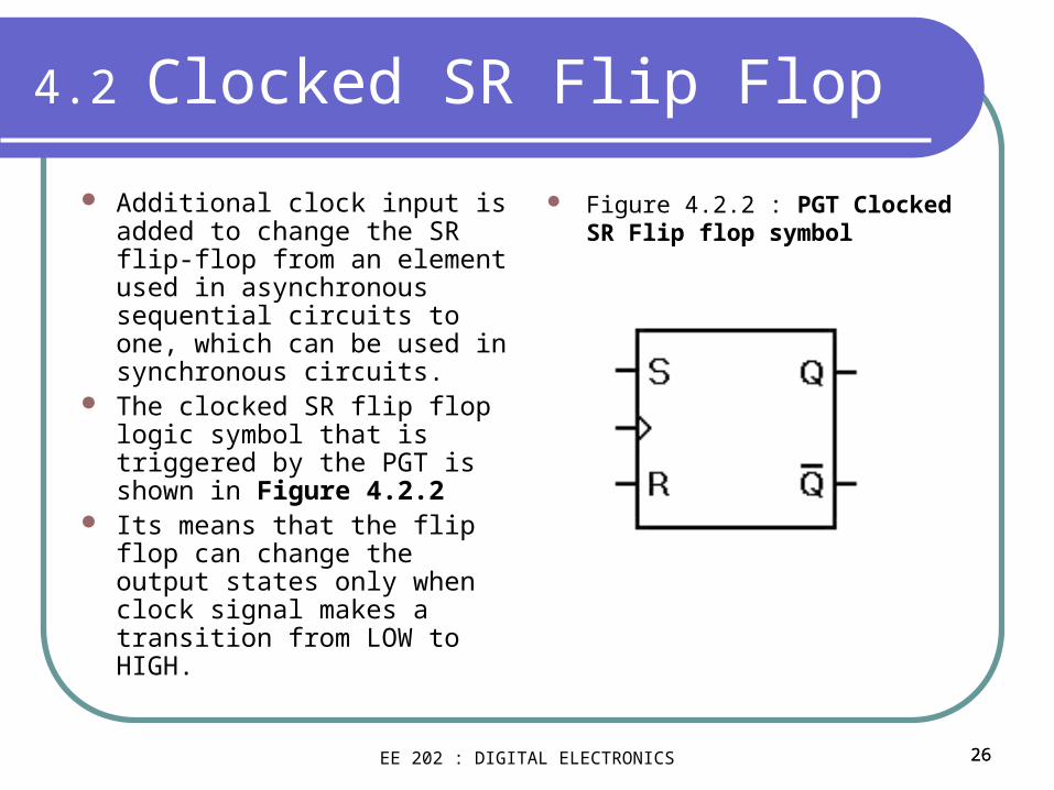
4.2 Clocked SR Flip Flop
Additional clock input is added to change the SR flip-flop from an element used in asynchronous sequential circuits to one, which can be used in synchronous circuits.
The clocked SR flip flop logic symbol that is triggered by the PGT is shown in Figure 4.2.2
Its means that the flip flop can change the output states only when clock signal makes a transition from LOW to HIGH.
Figure 4.2.2 : PGT Clocked SR Flip flop symbol
EE 202 : DIGITAL ELECTRONICS 26
27
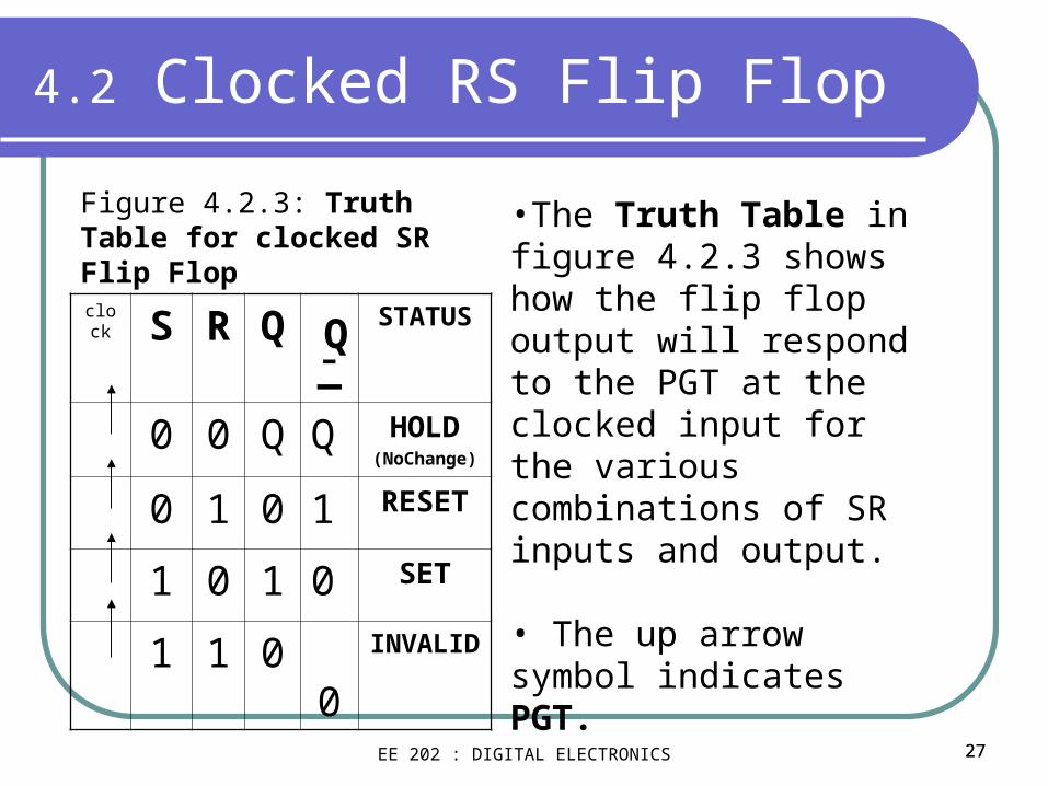
4.2 Clocked RS Flip Flop
Figure 4.2.3: Truth Table for clocked SR Flip Flop
clockS R Q ¯ STATUS
0 0 Q Q HOLD(NoChange)
0 1 0 1 RESET
1 0 1 0 SET
1 1 0 0 INVALID
•The Truth Table in figure 4.2.3 shows how the flip flop output will respond to the PGT at the clocked input for the various combinations of SR inputs and output.
• The up arrow symbol indicates PGT.
Q_
EE 202 : DIGITAL ELECTRONICS 27
28
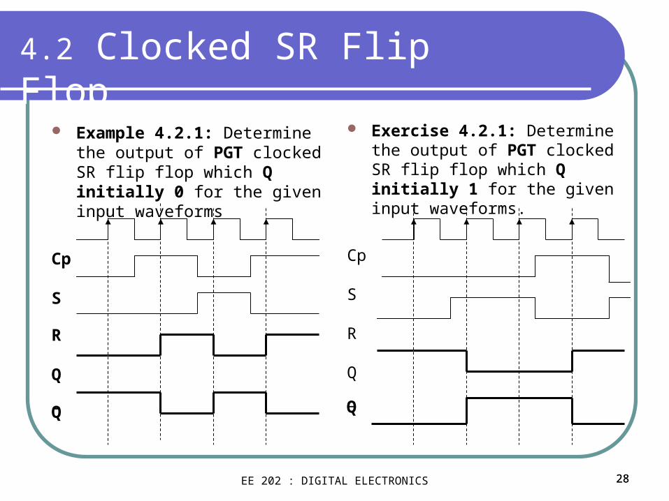
Example 4.2.1: Determine the output of PGT clocked SR flip flop which Q initially 0 for the given input waveforms
Cp
S
R
Q
¯
Exercise 4.2.1: Determine the output of PGT clocked SR flip flop which Q initially 1 for the given input waveforms.
Cp
S
R
Q
¯
4.2 Clocked SR Flip Flop
Q Q
EE 202 : DIGITAL ELECTRONICS 28
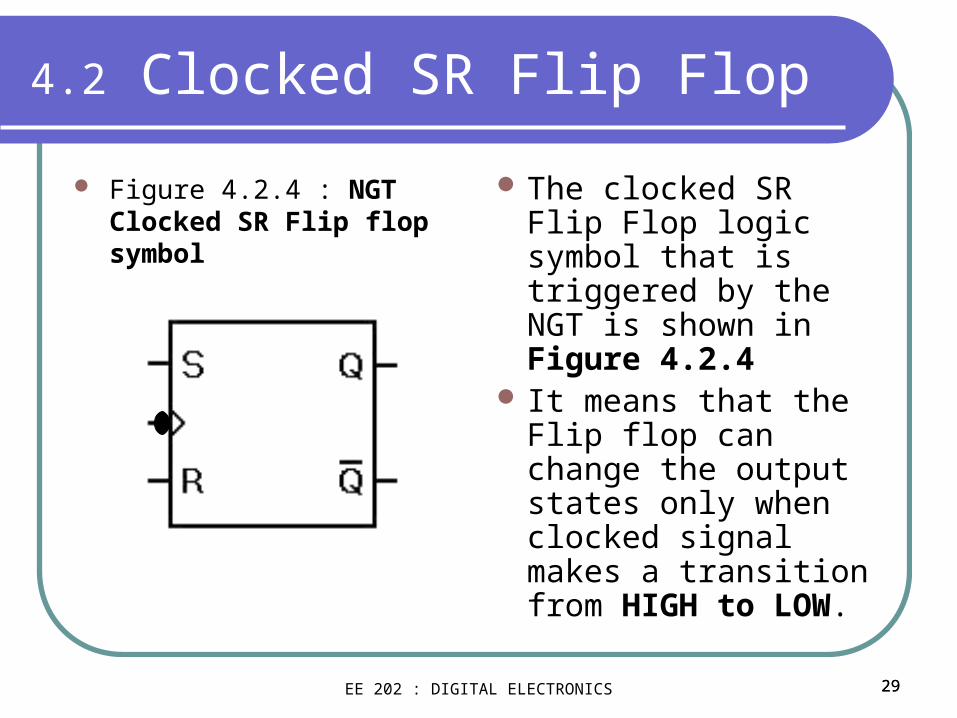
29
4.2 Clocked SR Flip Flop
Figure 4.2.4 : NGT Clocked SR Flip flop symbol
The clocked SR Flip Flop logic symbol that is triggered by the NGT is shown in Figure 4.2.4
It means that the Flip flop can change the output states only when clocked signal makes a transition from HIGH to LOW.
EE 202 : DIGITAL ELECTRONICS 29
30
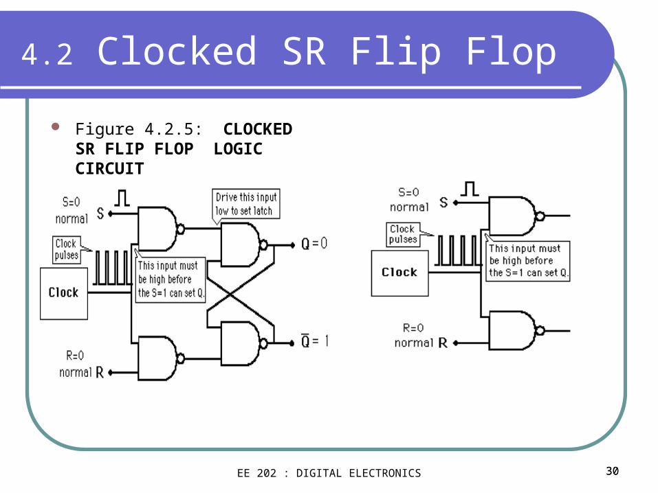
4.2 Clocked SR Flip Flop
Figure 4.2.5: CLOCKED SR FLIP FLOP LOGIC CIRCUIT
EE 202 : DIGITAL ELECTRONICS 30
31
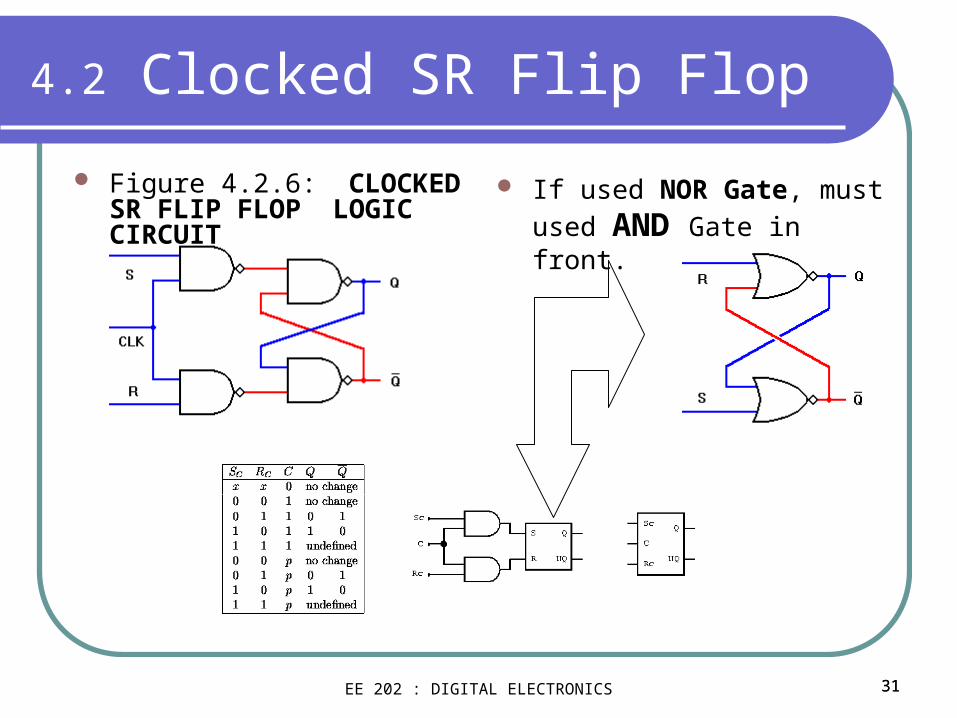
4.2 Clocked SR Flip Flop
Figure 4.2.6: CLOCKED SR FLIP FLOP LOGIC CIRCUIT
If used NOR Gate, must used
AND Gate in front.
EE 202 : DIGITAL ELECTRONICS 31
32
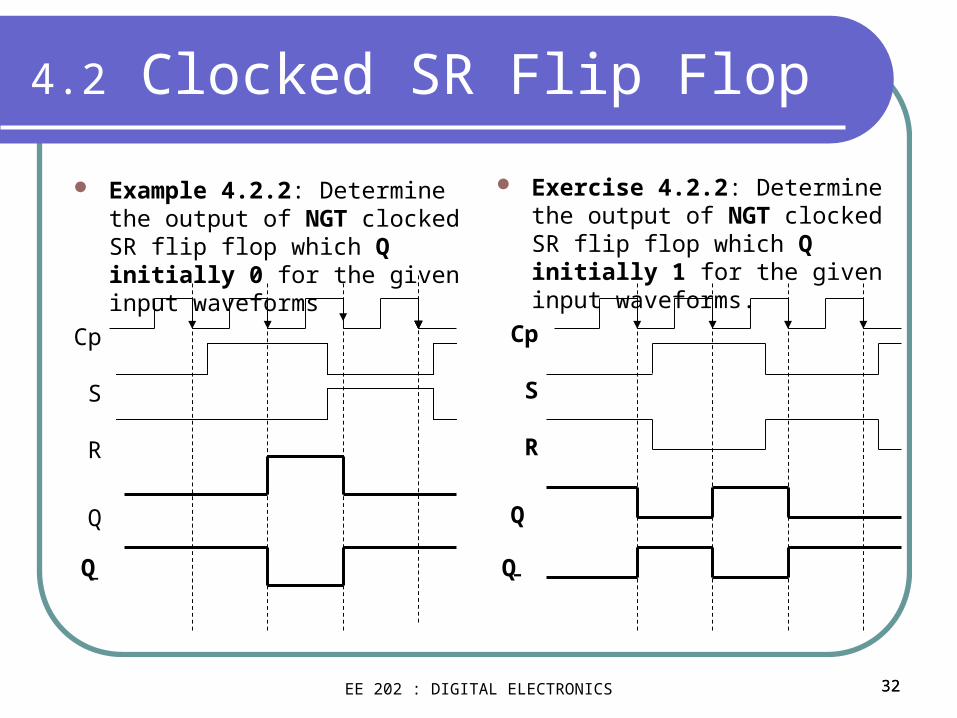
4.2 Clocked SR Flip Flop
Example 4.2.2: Determine the output of NGT clocked SR flip flop which Q initially 0 for the given input waveforms
Cp
S
R
Q
¯
Exercise 4.2.2: Determine the output of NGT clocked SR flip flop which Q initially 1 for the given input waveforms.
Cp
S
R
Q
¯Q Q
EE 202 : DIGITAL ELECTRONICS 32
33
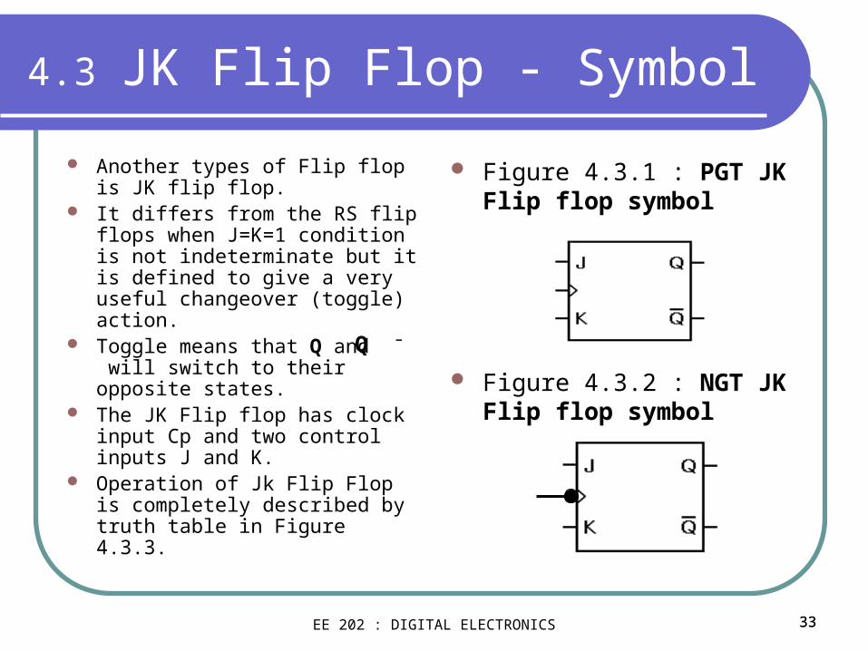
4.3 JK Flip Flop - Symbol
Another types of Flip flop is JK flip flop.
It differs from the RS flip flops when J=K=1 condition is not indeterminate but it is defined to give a very useful changeover (toggle) action.
Toggle means that Q and ¯ will switch to their opposite states.
The JK Flip flop has clock input Cp and two control inputs J and K.
Operation of Jk Flip Flop is completely described by truth table in Figure 4.3.3.
Figure 4.3.1 : PGT JK Flip flop symbol
Figure 4.3.2 : NGT JK Flip flop symbol
Q
EE 202 : DIGITAL ELECTRONICS 33
34
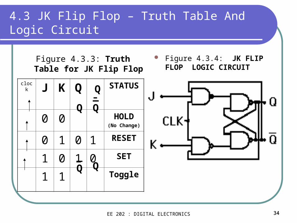
4.3 JK Flip Flop – Truth Table And Logic Circuit
Figure 4.3.3: Truth Table for JK Flip Flop
Figure 4.3.4: JK FLIP FLOP LOGIC CIRCUIT
clockJ K Q ¯ STATUS
0 0 HOLD(No Change)
0 1 0 1 RESET
1 0 1 0 SET
1 1 Toggle
Q
Q_Q
Q Q_
EE 202 : DIGITAL ELECTRONICS 34
35
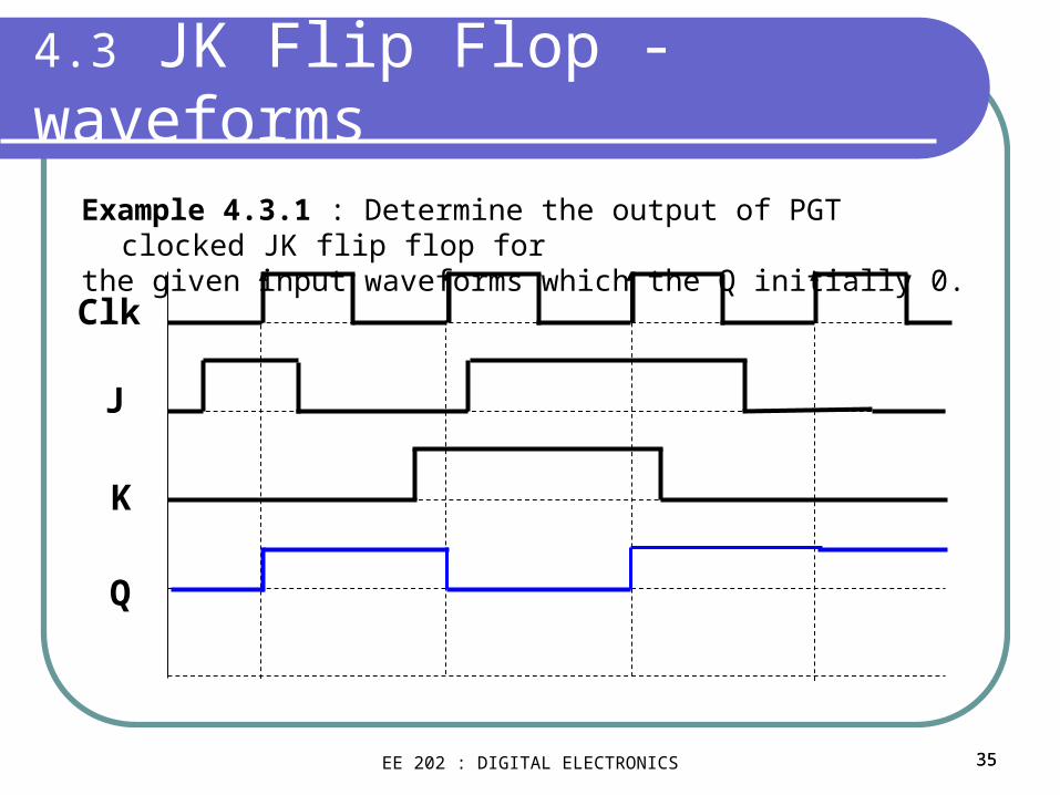
4.3 JK Flip Flop - waveforms
Example 4.3.1 : Determine the output of PGT clocked JK flip flop for the given input waveforms which the Q initially 0.
J
Clk
K
Q
EE 202 : DIGITAL ELECTRONICS 35
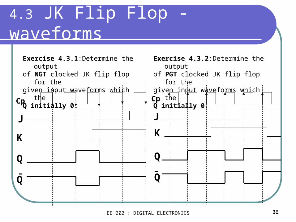
36
4.3 JK Flip Flop - waveforms
Exercise 4.3.1:Determine the output of NGT clocked JK flip flop for the given input waveforms which the Q initially 0.
Exercise 4.3.2:Determine the output of PGT clocked JK flip flop for the given input waveforms which the Q initially 0.
J
K
Q
Cp
Q̄
Cp Cp
K
J
Q
Q
¯
EE 202 : DIGITAL ELECTRONICS 36
37
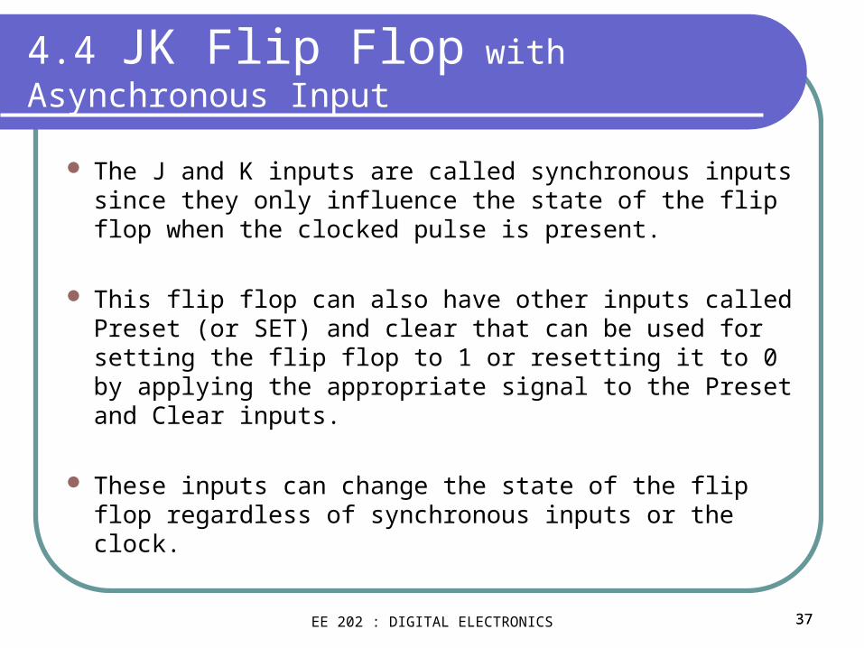
4.4 JK Flip Flop with Asynchronous Input
The J and K inputs are called synchronous inputs since they only influence the state of the flip flop when the clocked pulse is present.
This flip flop can also have other inputs called Preset (or SET) and clear that can be used for setting the flip flop to 1 or resetting it to 0 by applying the appropriate signal to the Preset and Clear inputs.
These inputs can change the state of the flip flop regardless of synchronous inputs or the clock.
EE 202 : DIGITAL ELECTRONICS 37
38
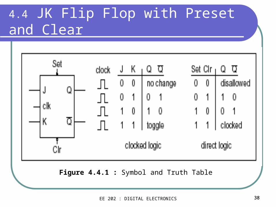
4.4 JK Flip Flop with Preset and Clear
Figure 4.4.1 : Symbol and Truth Table
EE 202 : DIGITAL ELECTRONICS 38
39
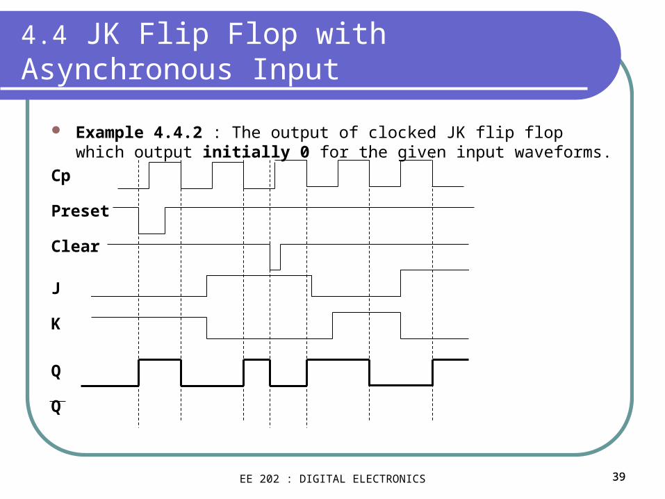
4.4 JK Flip Flop with Asynchronous Input
Example 4.4.2 : The output of clocked JK flip flop which output initially 0 for the given input waveforms.
Cp
Preset
Clear
J
K
Q
Q
EE 202 : DIGITAL ELECTRONICS 39
40
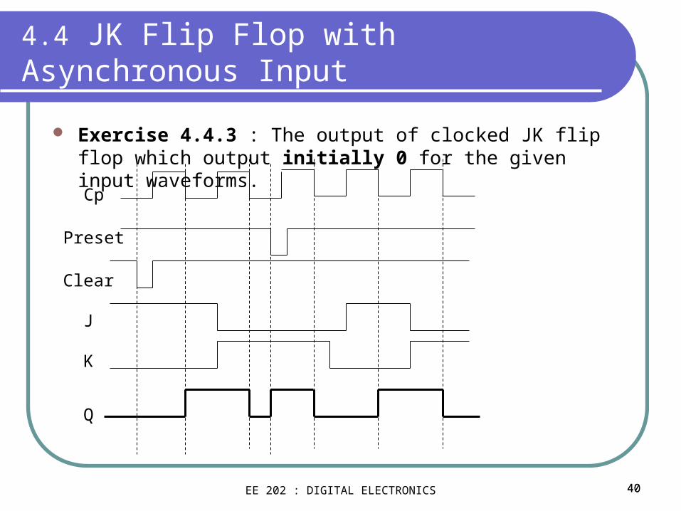
4.4 JK Flip Flop with Asynchronous Input
Exercise 4.4.3 : The output of clocked JK flip flop which output initially 0 for the given input waveforms.
Cp
Preset
J
K
Clear
Q
EE 202 : DIGITAL ELECTRONICS 40
41
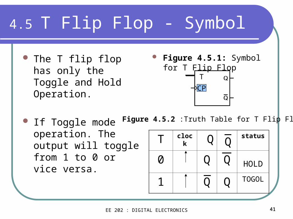
4.5 T Flip Flop - Symbol
The T flip flop has only the Toggle and Hold Operation.
If Toggle mode operation. The output will toggle from 1 to 0 or vice versa.
Figure 4.5.1: Symbol for T Flip Flop
T clock Q status
0 Q Q HOLD
1 Q Q TOGOL
Q
Figure 4.5.2 :Truth Table for T Flip Flop
CP
T
EE 202 : DIGITAL ELECTRONICS 41
42
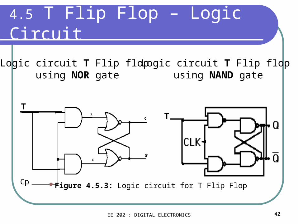
4.5 T Flip Flop – Logic Circuit
Cp
TT
Logic circuit T Flip flop using NOR gate
Logic circuit T Flip flop using NAND gate
Figure 4.5.3: Logic circuit for T Flip Flop
EE 202 : DIGITAL ELECTRONICS 42
43
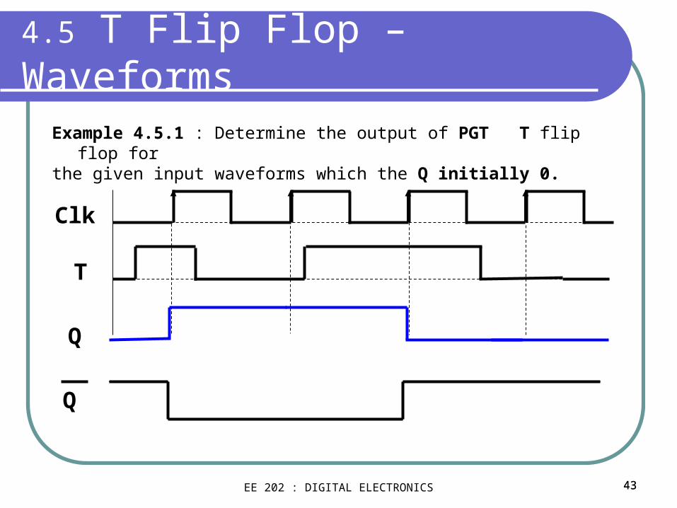
4.5 T Flip Flop – Waveforms
Example 4.5.1 : Determine the output of PGT T flip flop for the given input waveforms which the Q initially 0.
T
Clk
Q
Q
EE 202 : DIGITAL ELECTRONICS 43
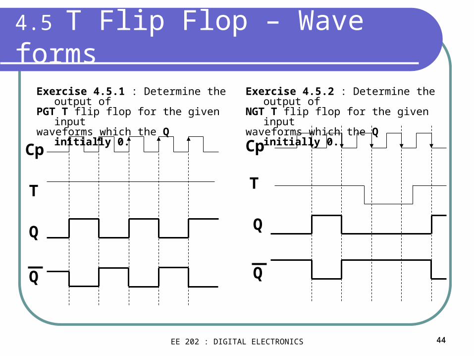
44
4.5 T Flip Flop – Wave forms
Exercise 4.5.1 : Determine the output of PGT T flip flop for the given input waveforms which the Q initially 0.
Exercise 4.5.2 : Determine the output of NGT T flip flop for the given input waveforms which the Q initially 0.
CpCp
Q
T
Q
Q
T
Q
EE 202 : DIGITAL ELECTRONICS 44
45
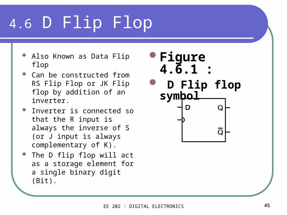
4.6 D Flip Flop
Also Known as Data Flip flop Can be constructed from RS
Flip Flop or JK Flip flop by addition of an inverter.
Inverter is connected so that the R input is always the inverse of S (or J input is always complementary of K).
The D flip flop will act as a storage element for a single binary digit (Bit).
Figure 4.6.1 : D Flip flop symbol
EE 202 : DIGITAL ELECTRONICS 45
46
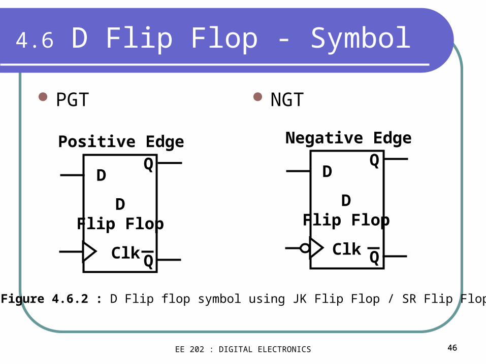
4.6 D Flip Flop - Symbol
PGT NGT
D
Clk
Q
Q
DFlip Flop
Positive Edge
D
Clk
Q
Q
DFlip Flop
Negative Edge
Figure 4.6.2 : D Flip flop symbol using JK Flip Flop / SR Flip Flop
EE 202 : DIGITAL ELECTRONICS 46
47
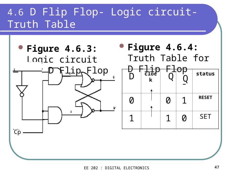
4.6 D Flip Flop- Logic circuit-Truth Table
Figure 4.6.3: Logic circuit for D Flip Flop
Figure 4.6.4: Truth Table for D Flip Flop
D clock Q ¯ status
0 0 1 RESET
1 1 0 SET
Q
Cp
EE 202 : DIGITAL ELECTRONICS 47
48
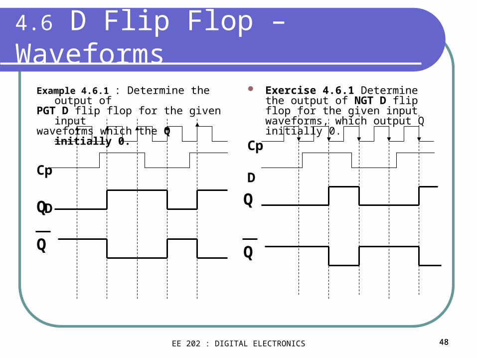
4.6 D Flip Flop – Waveforms
Example 4.6.1 : Determine the output of PGT D flip flop for the given input waveforms which the Q initially 0.
Cp
D
Exercise 4.6.1 Determine the output of NGT D flip flop for the given input waveforms, which output Q initially 0.
Cp
D
Q
Q
Q
Q
EE 202 : DIGITAL ELECTRONICS 48
49
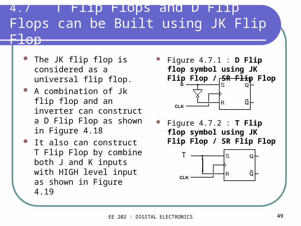
4.7 T Flip Flops and D Flip Flops can be Built using JK Flip Flop
The JK flip flop is considered as a universal flip flop.
A combination of Jk flip flop and an inverter can construct a D Flip Flop as shown in Figure 4.18
It also can construct T Flip Flop by combine both J and K inputs with HIGH level input as shown in Figure 4.19
Figure 4.7.1 : D Flip flop symbol using JK Flip Flop / SR Flip Flop
Figure 4.7.2 : T Flip flop symbol using JK Flip Flop / SR Flip Flop
T
EE 202 : DIGITAL ELECTRONICS 49
The END…….
50EE 202 : DIGITAL ELECTRONICS 50