Embed Size (px)
Citation preview
Digital Design 2eCopyright © 2010Frank Vahid
1
Digital DesignChapter 4:
Datapath Components
Copyright © 2010 Frank VahidInstructors of courses requiring Vahid's Digital Design textbook (published by John Wiley and Sons) have permission to modify and use these slides for customary course-related activities, subject to keeping this copyright notice in place and unmodified. These slides may be posted as unanimated pdf versions on publicly-accessible course websites.. PowerPoint source (or pdf with animations) may not be posted to publicly-accessible websites, but may be posted for students on internal protected sites or distributed directly to students by other electronic means. Instructors may make printouts of the slides available to students for a reasonable photocopying charge, without incurring royalties. Any other use requires explicit permission. Instructors may obtain PowerPoint source or obtain special use permissions from Wiley – see http://www.ddvahid.com for information.
Slides to accompany the textbook Digital Design, with RTL Design, VHDL, and Verilog, 2nd Edition,
by Frank Vahid, John Wiley and Sons Publishers, 2010. http://www.ddvahid.com
Digital Design 2eCopyright © 2010Frank Vahid
2
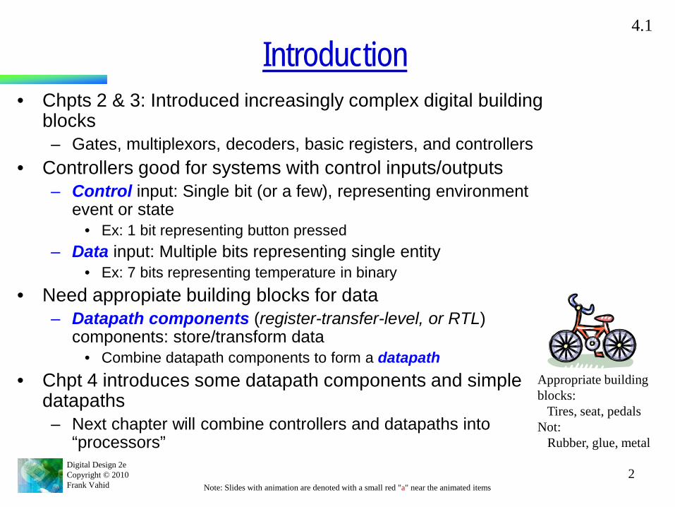
Introduction• Chpts 2 & 3: Introduced increasingly complex digital building
blocks– Gates, multiplexors, decoders, basic registers, and controllers
• Controllers good for systems with control inputs/outputs– Control input: Single bit (or a few), representing environment
event or state• Ex: 1 bit representing button pressed
– Data input: Multiple bits representing single entity• Ex: 7 bits representing temperature in binary
• Need appropiate building blocks for data– Datapath components (register-transfer-level, or RTL)
components: store/transform data• Combine datapath components to form a datapath
• Chpt 4 introduces some datapath components and simple datapaths– Next chapter will combine controllers and datapaths into
“processors”
4.1
Note: Slides with animation are denoted with a small red "a" near the animated items
Appropriate building blocks:
Tires, seat, pedalsNot:
Rubber, glue, metal
Digital Design 2eCopyright © 2010Frank Vahid
3
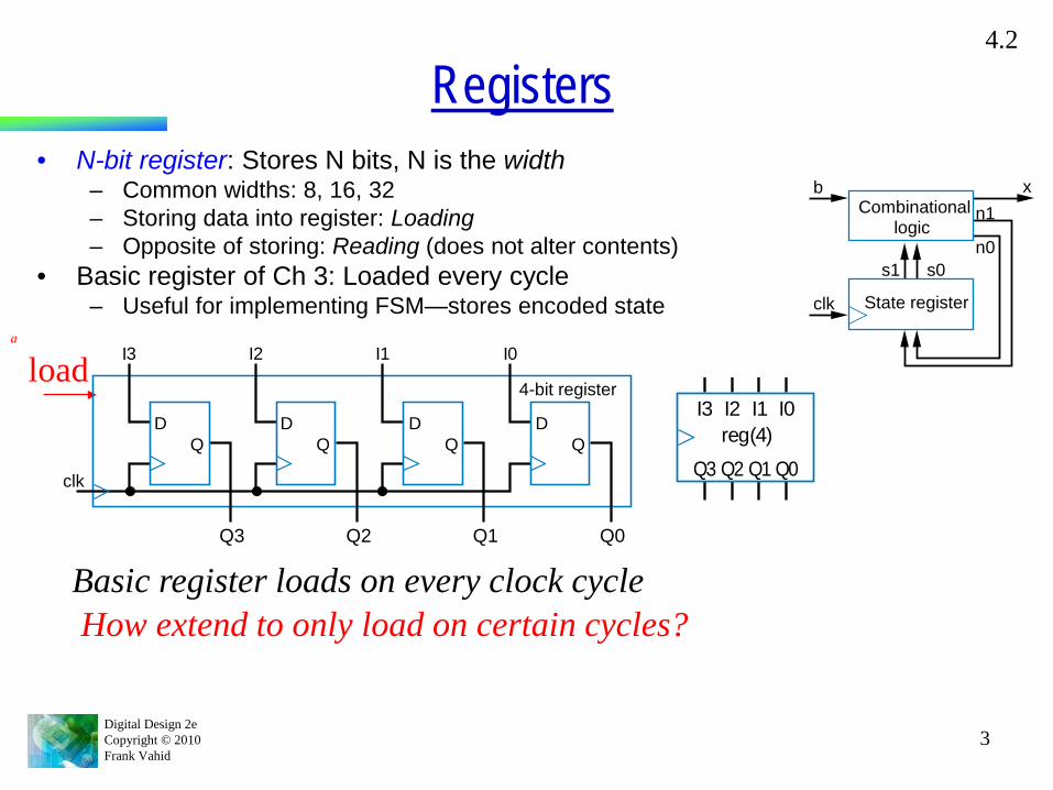
Registers• N-bit register: Stores N bits, N is the width
– Common widths: 8, 16, 32– Storing data into register: Loading– Opposite of storing: Reading (does not alter contents)
• Basic register of Ch 3: Loaded every cycle– Useful for implementing FSM—stores encoded state
4.2
Combinationallogic
State register
s1 s0
n1
n0
xb
clk
I3 I2 I1 I0
Q3 Q2 Q1 Q0reg(4)
Basic register loads on every clock cycle
load
How extend to only load on certain cycles?
a
DQ
DQ
DQ
DQ
I2I3
Q2Q3 Q1 Q0
I1 I0
clk
4-bit register
Digital Design 2eCopyright © 2010Frank Vahid
4
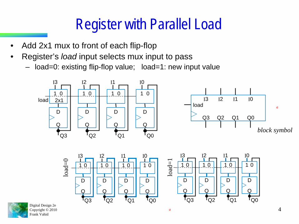
Register with Parallel Load• Add 2x1 mux to front of each flip-flop• Register’s load input selects mux input to pass
– load=0: existing flip-flop value; load=1: new input value
D
Q
Q3
I3
D
Q
Q2
I2
D
Q
Q1
I1
D
Q
Q0
I0
1 02x1load
1 0 1 0 1 0
a
a
1 0
D
Q
Q3
I3
1 0
D
Q
Q2
I2
1 0
Q
Q1
I1
1 0
D
Q
Q0
I0
D
load
=0 1 0
D
Q
Q3
I3
1 0
D
Q
Q2
I2
1 0
D
Q
Q1
I1
1 0
D
Q
Q0
I0
load
=1
loadI3 I2 I1 I0
Q3 Q2 Q1 Q0
block symbol
Digital Design 2eCopyright © 2010Frank Vahid
5
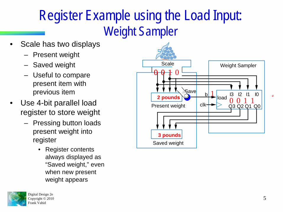
Register Example using the Load Input: Weight Sampler
• Scale has two displays– Present weight– Saved weight– Useful to compare
present item with previous item
• Use 4-bit parallel load register to store weight– Pressing button loads
present weight into register
• Register contents always displayed as “Saved weight,” even when new present weight appears
Scale
Saved weight
Weight Sampler
Present weight clk
bSave I3 I2 I1 I0
Q3 Q2 Q1 Q0
load3 pounds
0 0 1 1
0 0 1 1
3 pounds
0 0 1 0
2 pounds 1 a
Digital Design 2eCopyright © 2010Frank Vahid
6
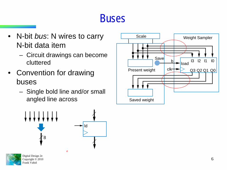
Buses• N-bit bus: N wires to carry
N-bit data item– Circuit drawings can become
cluttered
• Convention for drawing buses– Single bold line and/or small
angled line across
Scale
Saved weight
Weight Sampler
Present weight clk
bSave I3 I2 I1 I0
Q3 Q2 Q1 Q0
load
8
ld
a
Digital Design 2eCopyright © 2010Frank Vahid
7
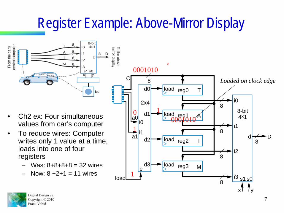
Register Example: Above-Mirror Display
C
d0
d1
d2
d3e
i0
i0
i1
i2
i3
a0
a1
load
i1
2x4 8
8
8
8
8Dd
8x y
s1 s0
8-bit4×1
load
load
load
load
reg0
reg1
reg2
reg3
T
A
I
M
• Ch2 ex: Four simultaneous values from car’s computer
• To reduce wires: Computer writes only 1 value at a time, loads into one of four registers
– Was: 8+8+8+8 = 32 wires– Now: 8 +2+1 = 11 wires
0
1
0001010
1
1
0001010
Loaded on clock edge
a
Digital Design 2eCopyright © 2010Frank Vahid
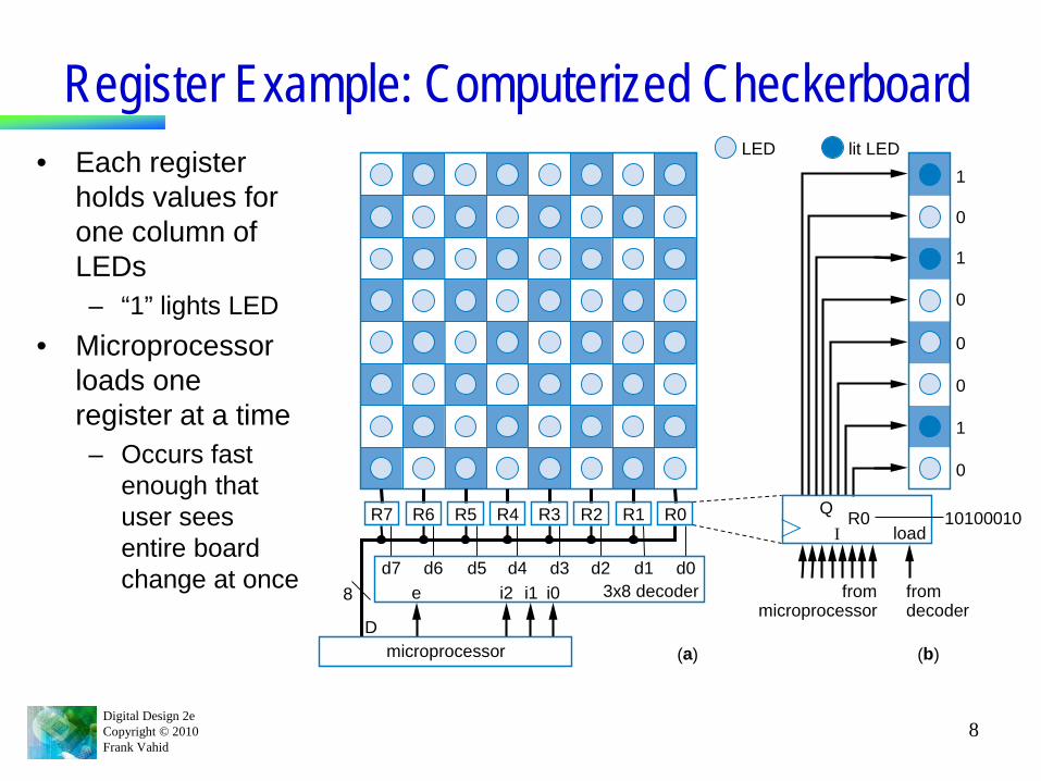
8
Register Example: Computerized Checkerboard• Each register
holds values for one column of LEDs– “1” lights LED
• Microprocessor loads one register at a time– Occurs fast
enough that user sees entire board change at once
LED
R7 R6
d6 d5 d4 d3 d2 d1 d0d78
D
R5 R4 R3 R2 R1 R0
e i2 i1 i0 3x8 decoder
microprocessor
lit LED1
1
0
0
0
0
0
1
QI
R0load
10100010
fromdecoder
frommicroprocessor
(b)(a)
Digital Design 2eCopyright © 2010Frank Vahid
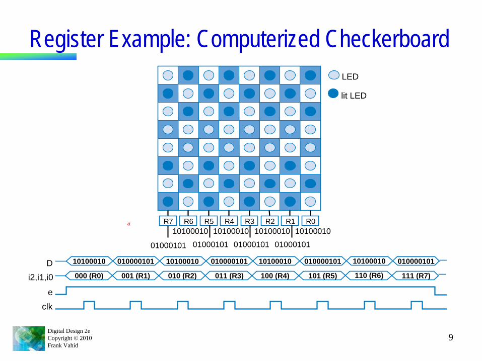
9
Register Example: Computerized Checkerboard
010000101 101000101010001010100010 10100010010000101 010000101 010000101
001 (R1) 100 (R4)010 (R2)000 (R0) 110 (R6)011 (R3) 101 (R5) 111 (R7)
clke
i2,i1,i0D
LED
lit LED
10100010 10100010 10100010 10100010
01000101 01000101 01000101 01000101
R7 R6 R5 R4 R3 R2 R1 R0a
Digital Design 2eCopyright © 2010Frank Vahid
10
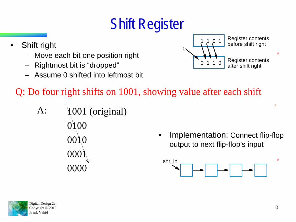
Shift Register• Shift right
– Move each bit one position right– Rightmost bit is “dropped”– Assume 0 shifted into leftmost bit
1 1 0 1 Register contentsbefore shift right
0 1 1 0
0
Register contentsafter shift right
a
Q: Do four right shifts on 1001, showing value after each shifta
A: 1001 (original)0100 0010 0001 0000
shr_in
• Implementation: Connect flip-flop output to next flip-flop’s input
a
Digital Design 2eCopyright © 2010Frank Vahid
11
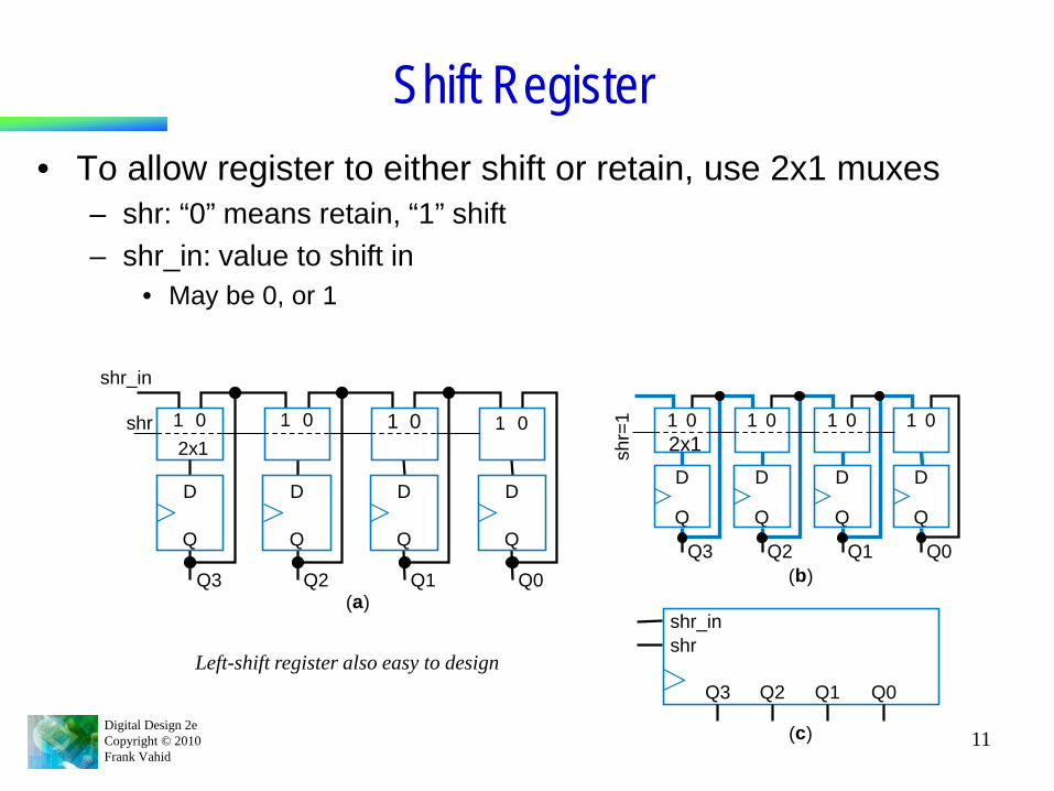
Shift Register• To allow register to either shift or retain, use 2x1 muxes
– shr: “0” means retain, “1” shift– shr_in: value to shift in
• May be 0, or 1
1 02x1D
Q
Q3
1 0
D
Q
Q2
1 0
D
Q
Q1
1 0
D
Q
Q0
1 02x1
D
Q
Q3
shr
shr_in
shrshr_in
1 0
D
Q
Q2
1 0
D
Q
Q1 (b)
(c)
(a)
1 0
D
Q
Q0
Q3 Q2 Q1 Q0Left-shift register also easy to design
shr=
1
Digital Design 2eCopyright © 2010Frank Vahid
12
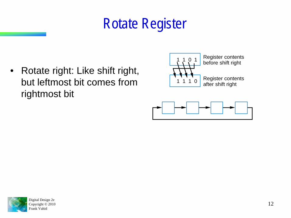
Rotate Register
• Rotate right: Like shift right, but leftmost bit comes from rightmost bit
1 1 0 1
1 1 1 0
Register contentsbefore shift right
Register contentsafter shift right
Digital Design 2eCopyright © 2010Frank Vahid
13
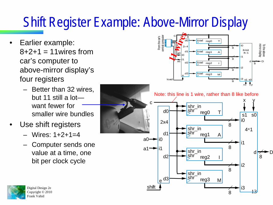
Shift Register Example: Above-Mirror Display• Earlier example:
8+2+1 = 11wires from car’s computer to above-mirror display’s four registers– Better than 32 wires,
but 11 still a lot—want fewer for smaller wire bundles
• Use shift registers– Wires: 1+2+1=4– Computer sends one
value at a time, one bit per clock cycle
C
d0
d1
d2
d3e
i0
i0
i1
i2
i3
a0
a1
load
i1
2×4
From
the ca
r'sce
ntralc
ompu
ter
8
8
8
8
8Dd
8x y
s1 s0
8-bit4×1
To the abovemirror display
load
load
load
load
reg0
reg1
reg2
reg3
T
A
I
M
c
d0
d1
d2
d3e
i0
i0s1 s0
x y
i1
i2
i3
a0
a1
shift
i1
2x4 8
8
8
8Dd
8
4×1
shrshr_in
shrshr_in
shrshr_in
shrshr_in
reg0
reg1
reg2
reg3
T
A
I
M
Note: this line is 1 wire, rather than 8 like before
Digital Design 2eCopyright © 2010Frank Vahid
14
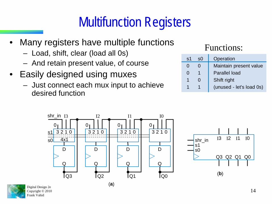
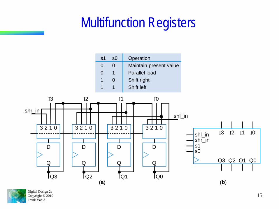
Multifunction Registers• Many registers have multiple functions
– Load, shift, clear (load all 0s)– And retain present value, of course
• Easily designed using muxes– Just connect each mux input to achieve
desired function
Functions:OperationMaintain present valueParallel loadShift right(unused - let's load 0s)
s00101
s10011
s1
shr_in
s0
3 2 1
I3
0
D
Q
Q3
Q2 Q1 Q0Q3
I2 I1 I0I3
Q2
03 2 1
I2
0
D
Q
0
Q1
3 2 1
I1
0
D
Q
0
Q0
3 2 1
I0
0
D
Q
0
4x1 shr_ins1s0
(a)
(b)
Digital Design 2eCopyright © 2010Frank Vahid
15
Multifunction Registers
OperationMaintain present valueParallel loadShift rightShift left
s00101
s10011
shr_inshl_in
3 2 1
I3
0
D
Q
Q3
Q2 Q1 Q0Q3
I2 I1 I0I3
Q2
3 2 1
I2
0
D
Q
Q1
3 2 1
I1
0
D
Q
Q0
3 2 1
I0
0
D
Q
shl_inshr_ins1s0
(a) (b)
Digital Design 2eCopyright © 2010Frank Vahid
16
Maintain valueShift leftShift rightShift rightParallel loadParallel loadParallel loadParallel load
NoteOperations0s1
01110000
01001111
OutputsInputs
01010101
00110011
00001111
ld shr shl
Truth table for combinational circuit
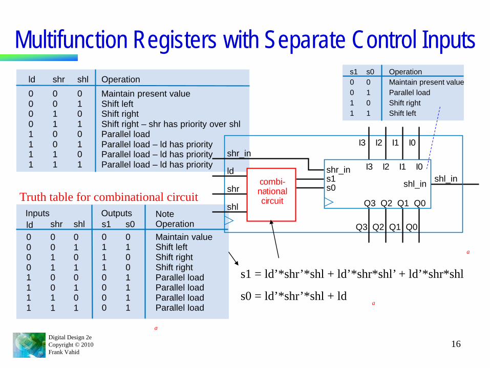
Multifunction Registers with Separate Control Inputs
Maintain present valueShift leftShift rightShift right – shr has priority over shlParallel loadParallel load – ld has priorityParallel load – ld has priorityParallel load – ld has priority
Operationshlshrld00001111
00110011
01010101
Q2 Q1 Q0Q3
Q2 Q1 Q0Q3
I2 I1 I0I3
I2 I1 I0I3
s1shr_in
shr_in
shr
shl
ld
s0shl_inshl_in
a
a
?combi-nationalcircuit
a
s1 = ld’*shr’*shl + ld’*shr*shl’ + ld’*shr*shl
s0 = ld’*shr’*shl + ld
OperationMaintain present valueParallel loadShift rightShift left
s00101
s10011
Digital Design 2eCopyright © 2010Frank Vahid
17
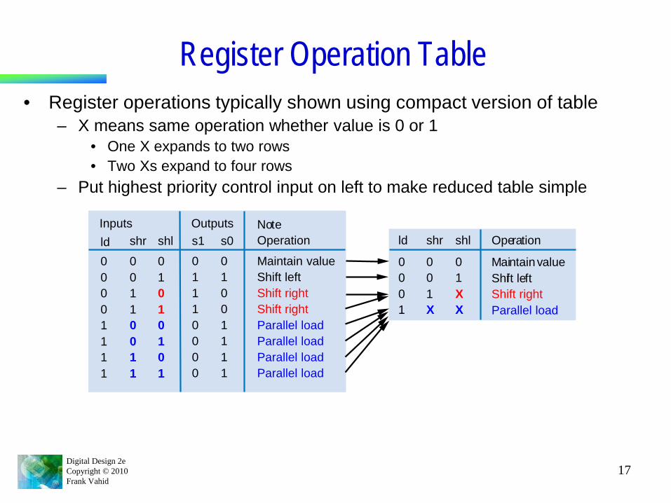
Register Operation Table• Register operations typically shown using compact version of table
– X means same operation whether value is 0 or 1• One X expands to two rows• Two Xs expand to four rows
– Put highest priority control input on left to make reduced table simple
Maintain valueShift left
NoteOperations0s1
01
01
OutputsInputs
01
00
00
Shift rightShift right
11
00
01
11
00
Parallel loadParallel loadParallel loadParallel load
0000
1111
0101
0011
1111
ld shr shl
MaintainvalueShift left
Operationld shr shl
01
00
00
Parallel loadXX1Shift rightX10
Digital Design 2eCopyright © 2010Frank Vahid
18
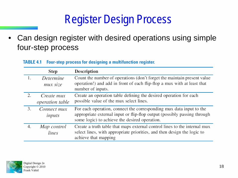
Register Design Process• Can design register with desired operations using simple
four-step process
Digital Design 2eCopyright © 2010Frank Vahid
19
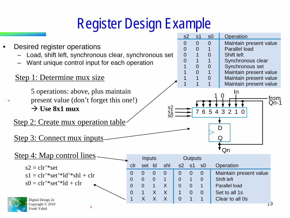
Register Design Example• Desired register operations
– Load, shift left, synchronous clear, synchronous set– Want unique control input for each operation
Step 1: Determine mux size
5 operations: above, plus maintain present value (don’t forget this one!) Use 8x1 mux
Step 2: Create mux operation table
Step 3: Connect mux inputs
Step 4: Map control lines
OperationMaintain present valueParallel loadShift leftSynchronous clearSynchronous setMaintain present valueMaintain present valueMaintain present value
s001010101
s100110011
s200001111
DQ
Qn
7 6 3 2 1
In
05 4
1 0
s2s1s0
fromQn-1
OperationMaintain present valueShift leftParallel loadSet to all 1sClear to all 0s
s000101
s101001
s200010
shl01XXX
ld001XX
clr00001
Inputs Outputsset0001X
a
a
s2 = clr’*sets1 = clr’*set’*ld’*shl + clrs0 = clr’*set’*ld + clr
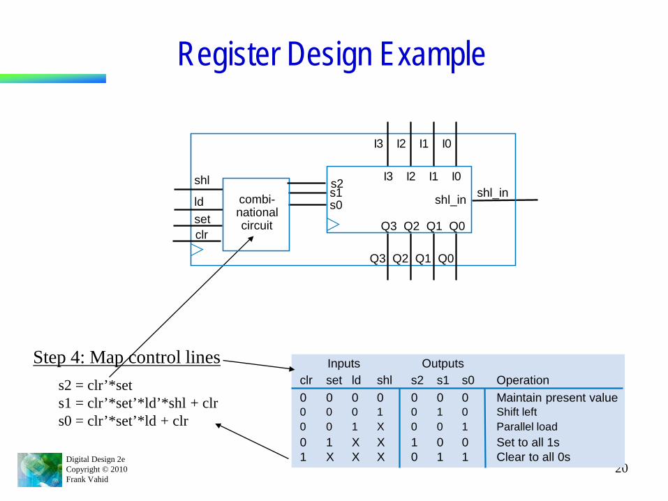
Digital Design 2eCopyright © 2010Frank Vahid
20
Register Design Example
Step 4: Map control linesOperationMaintain present valueShift leftParallel loadSet to all 1sClear to all 0s
s000101
s101001
s200010
shl01XXX
ld001XX
clr00001
Inputs Outputsset0001X
s2 = clr’*sets1 = clr’*set’*ld’*shl + clrs0 = clr’*set’*ld + clr
Q2 Q1 Q0Q3
Q2 Q1 Q0Q3
I2 I1 I0I3
I2 I1 I0I3
s1ld
shl
s0shl_inshl_incombi-
nationalcircuitset
clr
s2
Digital Design 2eCopyright © 2010Frank Vahid
21
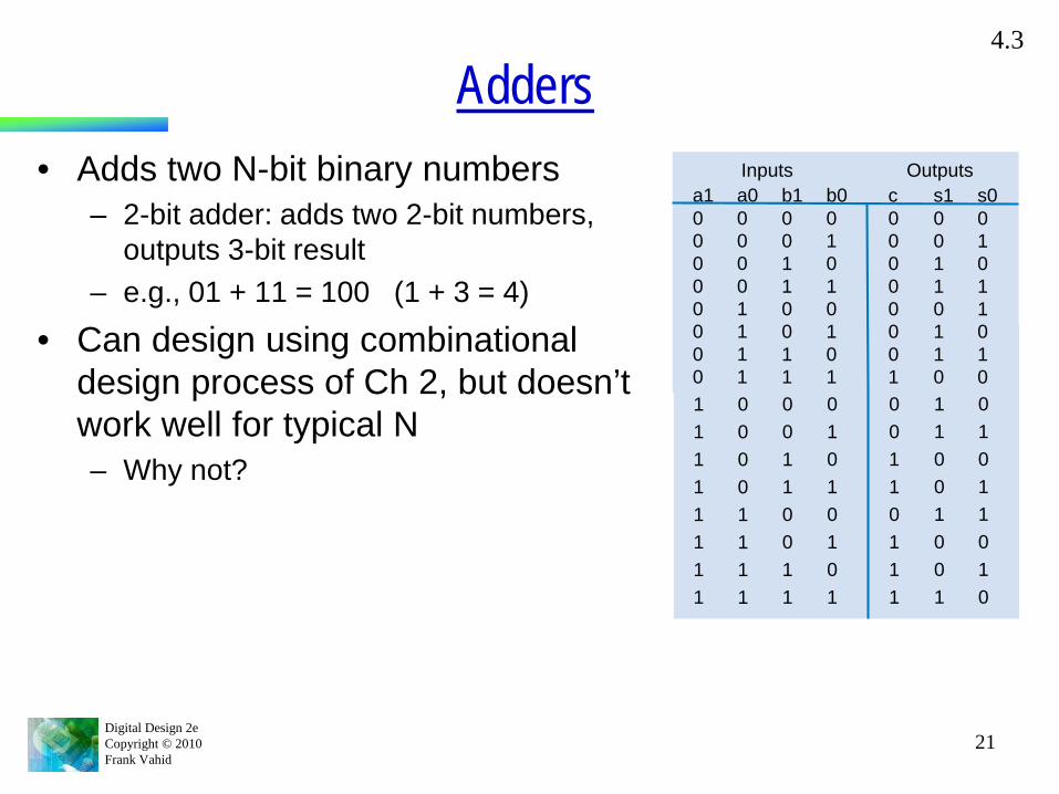
Adders• Adds two N-bit binary numbers
– 2-bit adder: adds two 2-bit numbers, outputs 3-bit result
– e.g., 01 + 11 = 100 (1 + 3 = 4)
• Can design using combinational design process of Ch 2, but doesn’t work well for typical N– Why not?
4.3
01011010
11001001
00110111
01010101
00110011
11111111
00001111
s001011010
s100110110
c00000001
b001010101
b100110011
a100000000
Inputs Outputsa000001111
Digital Design 2eCopyright © 2010Frank Vahid
22
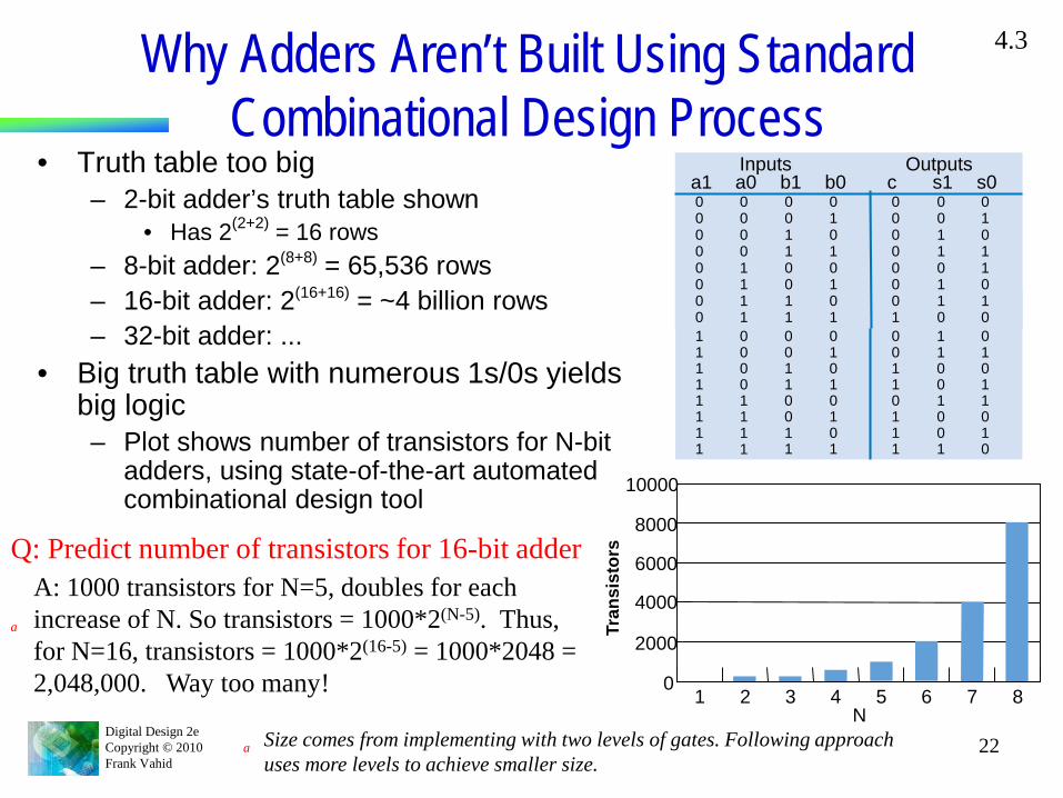
Why Adders Aren’t Built Using Standard Combinational Design Process
• Truth table too big– 2-bit adder’s truth table shown
• Has 2(2+2) = 16 rows– 8-bit adder: 2(8+8) = 65,536 rows– 16-bit adder: 2(16+16) = ~4 billion rows– 32-bit adder: ...
• Big truth table with numerous 1s/0s yields big logic– Plot shows number of transistors for N-bit
adders, using state-of-the-art automated combinational design tool
4.3
01011010
11001001
00110111
01010101
00110011
11111111
00001111
s001011010
s100110110
c00000001
b001010101
b100110011
a100000000
Inputs Outputsa000001111
Q: Predict number of transistors for 16-bit adderA: 1000 transistors for N=5, doubles for each increase of N. So transistors = 1000*2(N-5). Thus, for N=16, transistors = 1000*2(16-5) = 1000*2048 = 2,048,000. Way too many!
a
10000
8000
6000
4000
2000
01 2 3 4 5
N6 7 8
Tran
sist
ors
Size comes from implementing with two levels of gates. Following approach uses more levels to achieve smaller size.
a
Digital Design 2eCopyright © 2010Frank Vahid
23
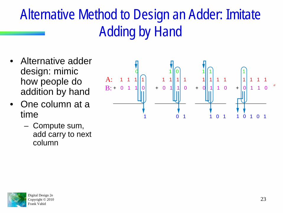
Alternative Method to Design an Adder: Imitate Adding by Hand
• Alternative adder design: mimic how people do addition by hand
• One column at a time– Compute sum,
add carry to next column
1 1 1 1+ 0 1 1 0
0
1
1 1 1 1
10
+ 0 1 1 0
011 1 1 1
101
+ 0 1 1 0
111 1 1 1
101
+ 0 1 1 0
1
01
A:B: a

Digital Design 2eCopyright © 2010Frank Vahid
24
Alternative Method to Design an Adder: Imitate Adding by Hand
• Create component for each column– Adds that
column’s bits, generates sum and carry bits
01 1 1 1
+ 0 1 1 0
1
10101
b
co s
0
a ci
A:
B:+ 0
1 1 1 1
1
b
co s
1
a ci
1
b
co s
0
a ci
1
1 1 0
b
co s
1 SUM
a
0
A:B:
1
Half-adderFull-adders
a
Digital Design 2eCopyright © 2010Frank Vahid
25
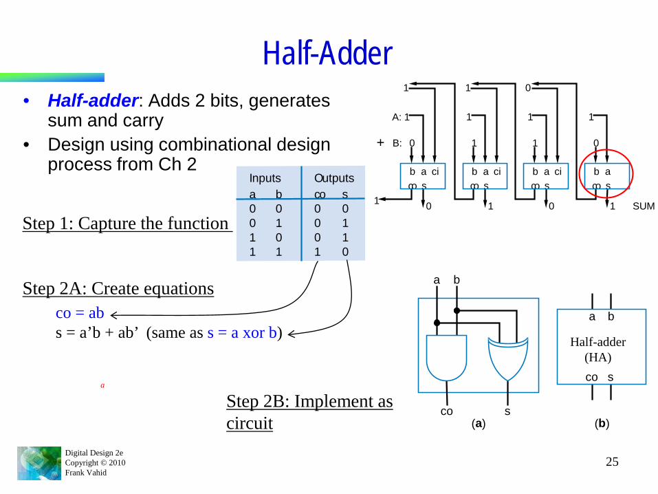
Half-Adder• Half-adder: Adds 2 bits, generates
sum and carry• Design using combinational design
process from Ch 2 bco s
0
a ci
A:
B:+ 0
1 1 1 1
1
1
bco s
1
a ci
1
1
bco s
0
a ci
1
0
bco s
1 SUM
a
0
s0110
co0001
b0101
a0011
Inputs Outputs
Step 1: Capture the function
Step 2A: Create equations
Step 2B: Implement as circuit
co = abs = a’b + ab’ (same as s = a xor b)
a b
co
co s
a b
s(a) (b)
Half-adder (HA)
a
Digital Design 2eCopyright © 2010Frank Vahid
26
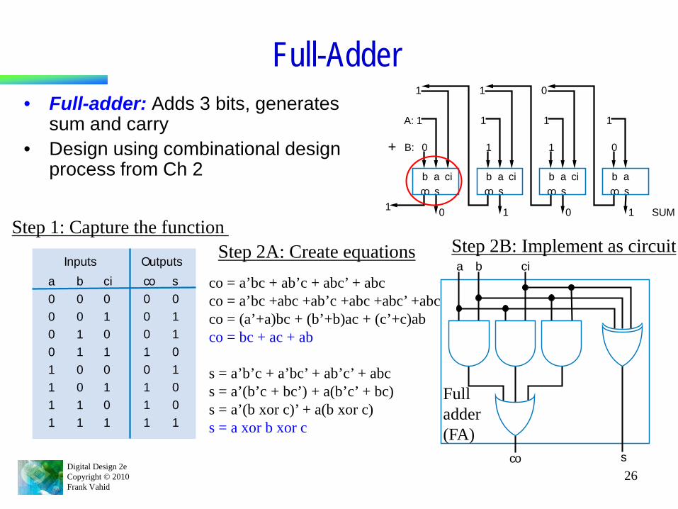
Full-Adder• Full-adder: Adds 3 bits, generates
sum and carry• Design using combinational design
process from Ch 2 bco s
0
a ci
A:
B:+ 0
1 1 1 1
1
1
bco s
1
a ci
1
1
bco s
0
a ci
1
0
bco s
1 SUM
a
0
Step 1: Capture the function
s01101001
co00010111
ci01010101
b00110011
a00001111
Inputs Outputs Step 2A: Create equationsco = a’bc + ab’c + abc’ + abcco = a’bc +abc +ab’c +abc +abc’ +abcco = (a’+a)bc + (b’+b)ac + (c’+c)abco = bc + ac + ab
s = a’b’c + a’bc’ + ab’c’ + abcs = a’(b’c + bc’) + a(b’c’ + bc)s = a’(b xor c)’ + a(b xor c)s = a xor b xor c
Step 2B: Implement as circuit
co
ciba
s
Full adder (FA)
Digital Design 2eCopyright © 2010Frank Vahid
27
Carry-Ripple Adder• Using half-adder and full-adders, we can build adder that adds like we
would by hand• Called a carry-ripple adder
– 4-bit adder shown: Adds two 4-bit numbers, generates 5-bit output• 5-bit output can be considered 4-bit “sum” plus 1-bit “carry out”
– Can easily build any size adder
a3
co s
FA
co
b3 a2b2
s3 s2 s1
ciba
co s
FA
ciba
a1b1
co s
FA
ciba
s0
a0 b0
co s
HA
ba
(a)
a3a2a1a0 b3
s3 s2 s1 s0co
b2b1b0
(b)
4-bit adder
Digital Design 2eCopyright © 2010Frank Vahid
28
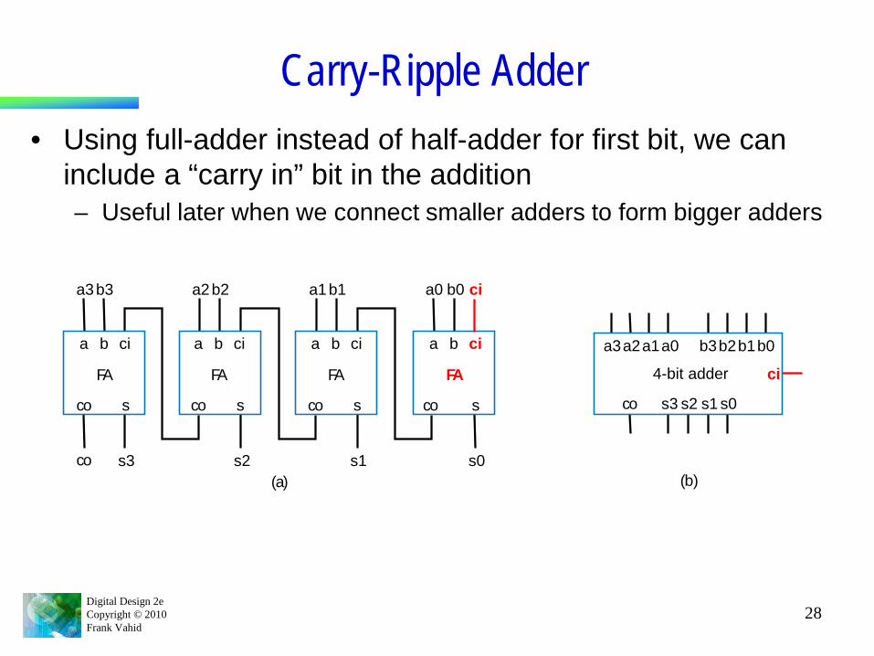
Carry-Ripple Adder• Using full-adder instead of half-adder for first bit, we can
include a “carry in” bit in the addition– Useful later when we connect smaller adders to form bigger adders
a3
co s
FA
co
b3 a2b2
s3 s2 s1
ciba
co s
FA
ciba
a1b1
co s
FA
ciba
s0
a0 b0 ci
co s
FA
ciba
(a)
a3a2a1a0 b3
s3 s2 s1 s0co
ci
b2b1b0
(b)
4-bit adder
Digital Design 2eCopyright © 2010Frank Vahid
29
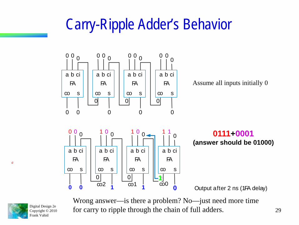
Carry-Ripple Adder’s Behavior
0 1 1 10 0 0 1 0111+0001(answer should be 01000)
0
co s
FA
0 0
0 0 0
0 0 00 0 0
0 0
ciba
co s
FAciba
0 0
co s
FAciba
0
0 0
co s
FAciba
0
Assume all inputs initially 0
Output after 2 ns (1FA delay)0 0 1 1 0
co s
FA
0 0
0 0 0
co2 co1 co0
ciba
co s
FAciba
co s
FAciba
co s
FAciba
0
01
Wrong answer—is there a problem? No—just need more time for carry to ripple through the chain of full adders.
a
Digital Design 2eCopyright © 2010Frank Vahid
30
0 00
co sFA
1 1 1
1 10 1 0
ciba
co sFA
ciba
1 0
co sFA
ciba
0 0 0
1 1
co sFA
ciba
(d)Output after 8ns (4 FA delays)
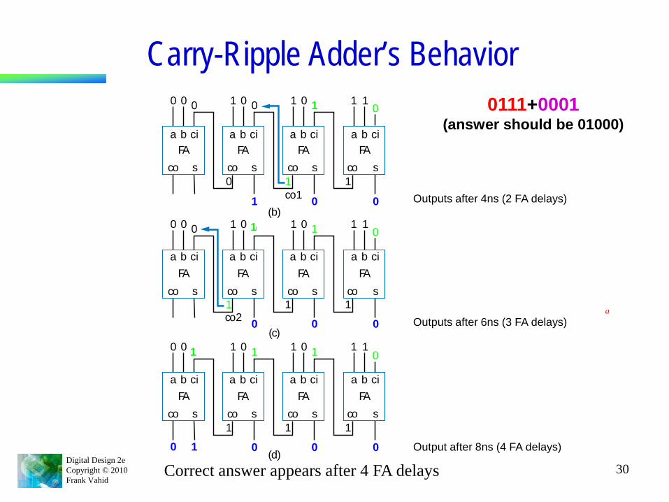
Carry-Ripple Adder’s Behavior0
co sFA
0 0 1
co1
0 1 0
ciba
co sFA
ciba
1 0
co sFA
ciba
1 0 0
1 1
co sFA
ciba
(b)
10 1
0
0
1
0 1
1
Outputs after 4ns (2 FA delays)
00
co sFA
1 1
0 1
co2
0 1 0
ciba
co sFA
ciba
1 0
co sFA
ciba
0 0
1 10
co sFA
ciba
(c)Outputs after 6ns (3 FA delays)
a
0111+0001(answer should be 01000)
1
Correct answer appears after 4 FA delays
Digital Design 2eCopyright © 2010Frank Vahid
31
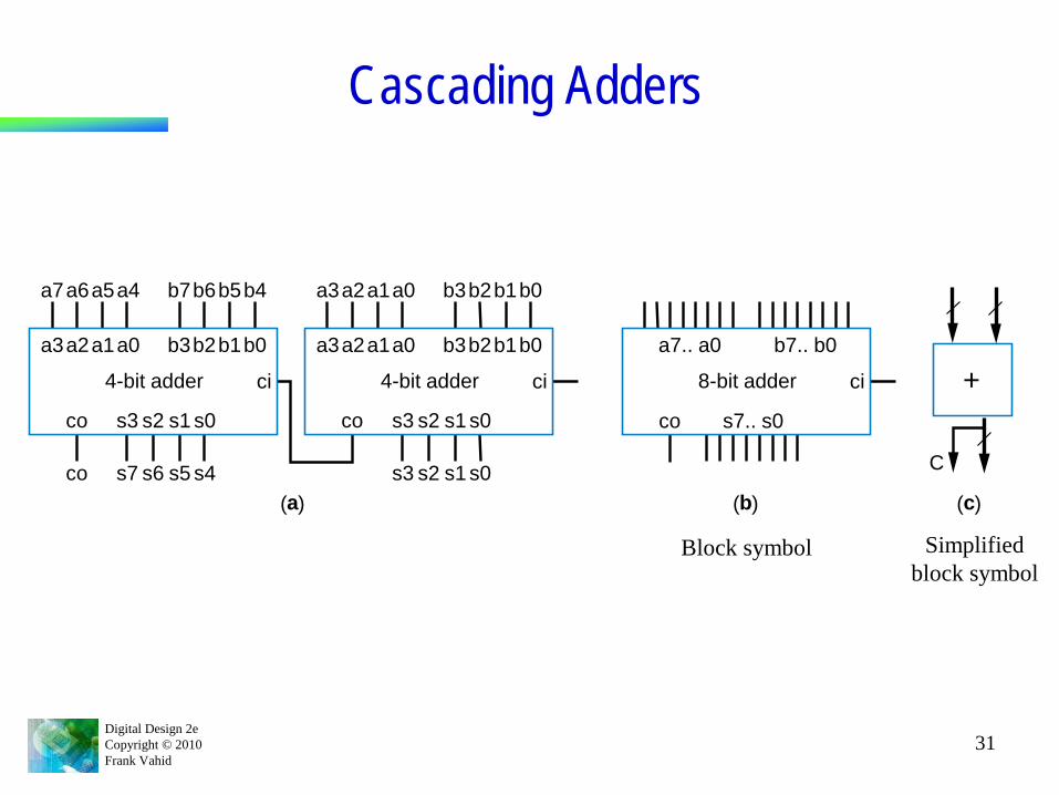
Cascading Adders
a3a2a1a0 b3
s3 s2 s1 s0co
s7 s6 s5 s4co
ci
b2b1b0
a7a6a5a4 b7b6b5b4
(a) (b)
4-bit adder
a3a2a1a0 b3
s3 s2 s1 s0
s3 s2 s1 s0
co
ci
b2b1b0
a3a2a1a0 b3b2b1b0
4-bit adder
a7.. a0 b7.. b0
s7.. s0co
ci8-bit adder +
C
(c)
Block symbol Simplifiedblock symbol
Digital Design 2eCopyright © 2010Frank Vahid
32
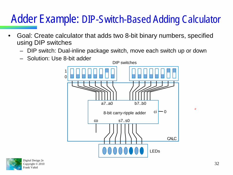
Adder Example: DIP-Switch-Based Adding Calculator• Goal: Create calculator that adds two 8-bit binary numbers, specified
using DIP switches– DIP switch: Dual-inline package switch, move each switch up or down– Solution: Use 8-bit adder
DIP switches
10
a7..a0 b7..b0
s7..s0
8-bit carry-ripple adder
co
ci 0
CALC
LEDs
a
Digital Design 2eCopyright © 2010Frank Vahid
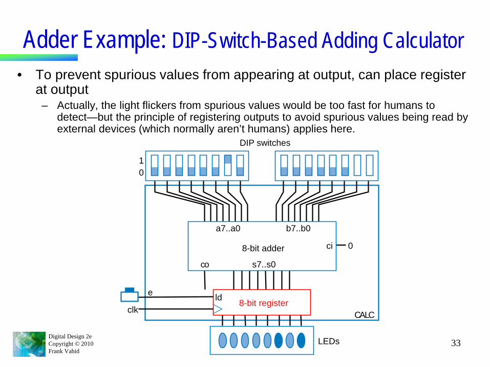
33
Adder Example: DIP-Switch-Based Adding Calculator• To prevent spurious values from appearing at output, can place register
at output– Actually, the light flickers from spurious values would be too fast for humans to
detect—but the principle of registering outputs to avoid spurious values being read by external devices (which normally aren’t humans) applies here.
DIP switches
10
a7..a0 b7..b0
s7..s0
8-bit adder
8-bit register
co
ci 0
CALC
LEDs
e
clkld
Digital Design 2eCopyright © 2010Frank Vahid
34
display register
to display
1 WeightAdjusterclk
ld
0 0 0 0 0
0
4
7
5
1
3
6 2weightsensor
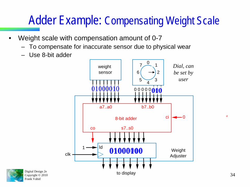
Adder Example: Compensating Weight Scale• Weight scale with compensation amount of 0-7
– To compensate for inaccurate sensor due to physical wear– Use 8-bit adder
a7..a0 b7..b0
s7..s0
8-bit adder
co
ci 0
01000010 000
01000010
010
01000100
a
Dial, can be set by
user
Digital Design 2eCopyright © 2010Frank Vahid
35
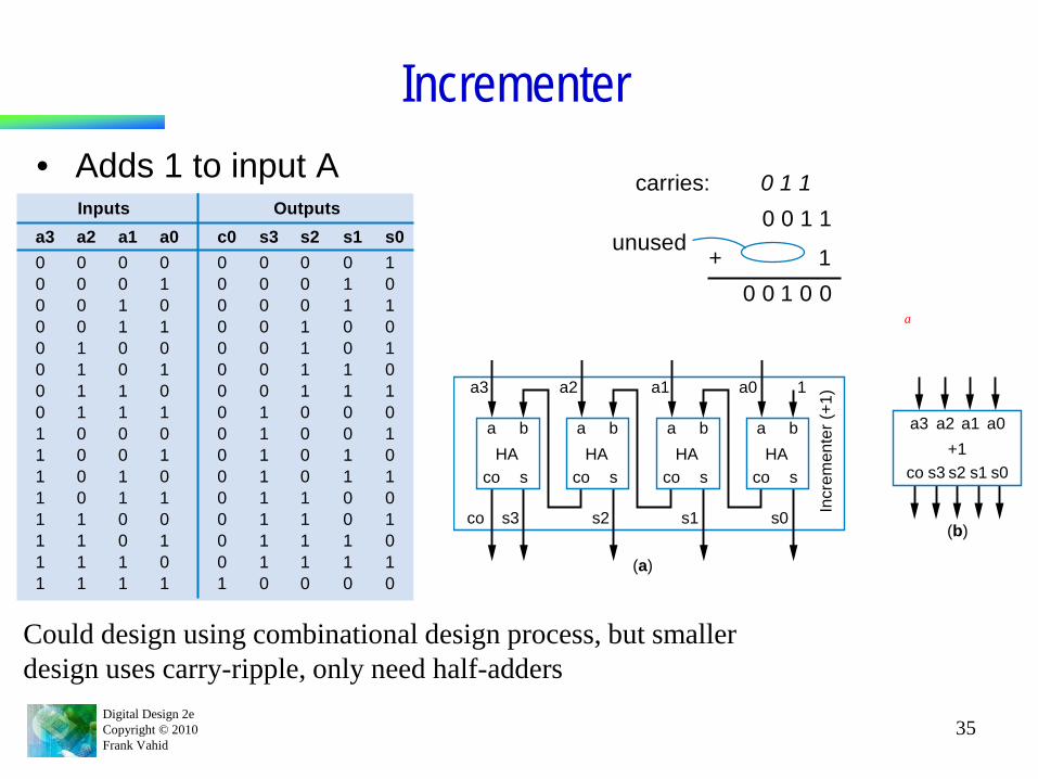
Incrementer• Adds 1 to input A
s20001111000011110
s10110011001100110
s01010101010101010
s30000000111111110
c00000000000000001
a00101010101010101
a10011001100110011
a30000000011111111
Inputs Outputsa20000111100001111
0 0 1 10 1 1
1+
carries:
unused
0000 1
(a)
(b)
a3 a2 a1 a0 1
s0s1s2s3co
a b
co sHA
a b
co sHA
a b
co sHA
a b
co sHA
Incr
emen
ter (
+1)
a3
co s3 s2+1
s1 s0
a2 a1 a0
a
Could design using combinational design process, but smaller design uses carry-ripple, only need half-adders
Digital Design 2eCopyright © 2010Frank Vahid
36
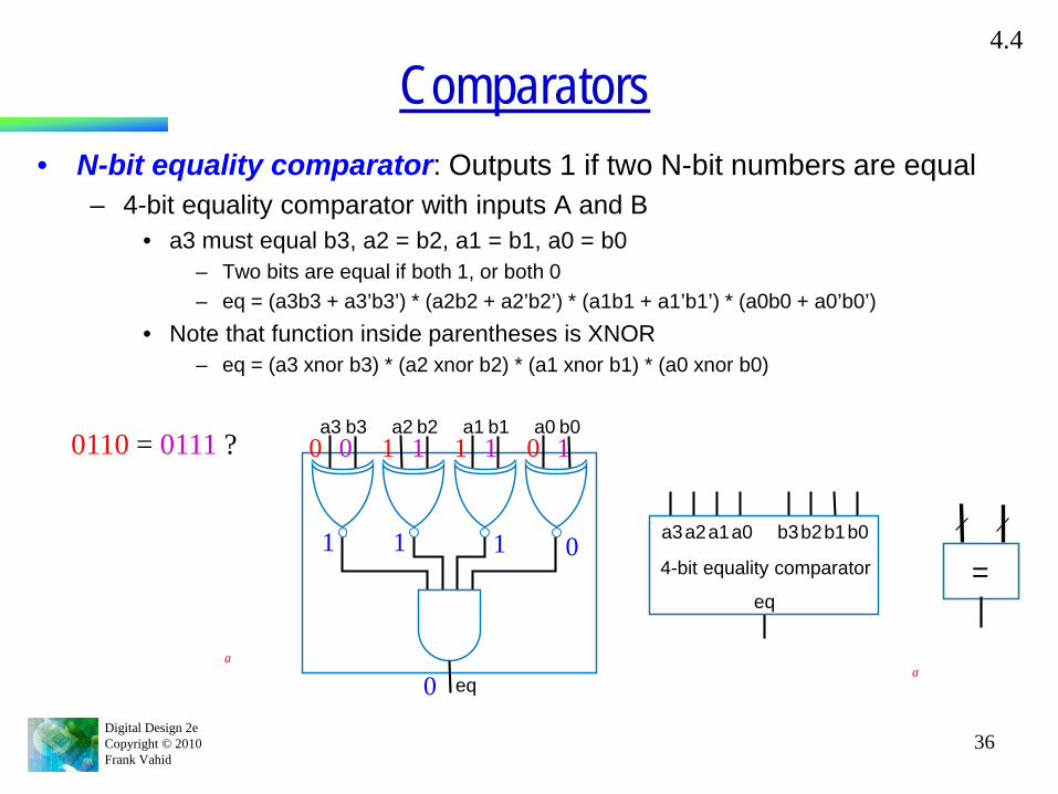
Comparators• N-bit equality comparator: Outputs 1 if two N-bit numbers are equal
– 4-bit equality comparator with inputs A and B• a3 must equal b3, a2 = b2, a1 = b1, a0 = b0
– Two bits are equal if both 1, or both 0– eq = (a3b3 + a3’b3’) * (a2b2 + a2’b2’) * (a1b1 + a1’b1’) * (a0b0 + a0’b0’)
• Note that function inside parentheses is XNOR– eq = (a3 xnor b3) * (a2 xnor b2) * (a1 xnor b1) * (a0 xnor b0)
4.4
a3 b3 a2 b2 a1 b1 a0 b0
eq
a3a2a1a0 b3
eq
b2b1b0
4-bit equality comparator
a
0110 = 0111 ? 0 1 1 00 1 1 1
01 1 1
0
=
a
Digital Design 2eCopyright © 2010Frank Vahid
37
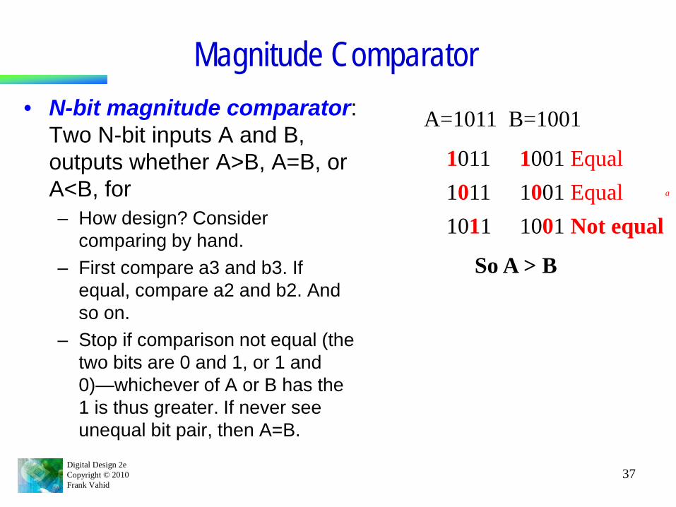
Magnitude Comparator• N-bit magnitude comparator:
Two N-bit inputs A and B, outputs whether A>B, A=B, or A<B, for– How design? Consider
comparing by hand. – First compare a3 and b3. If
equal, compare a2 and b2. And so on.
– Stop if comparison not equal (the two bits are 0 and 1, or 1 and 0)—whichever of A or B has the 1 is thus greater. If never see unequal bit pair, then A=B.
A=1011 B=1001
1011 1001a
Equal1011 1001 Equal1011 1001 Not equal
So A > B
Digital Design 2eCopyright © 2010Frank Vahid
38
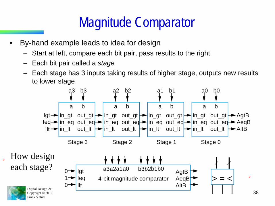
Magnitude Comparator• By-hand example leads to idea for design
– Start at left, compare each bit pair, pass results to the right– Each bit pair called a stage– Each stage has 3 inputs taking results of higher stage, outputs new results
to lower stage
in_gtin_eqin_lt
out_gtout_eqout_lt
IgtIeqIlt
Stage 3
a3 b3
a bin_gtin_eqin_lt
out_gtout_eqout_lt
Stage 2
a2 b2
a bin_gtin_eqin_lt
out_gtout_eqout_lt
Stage 1
a1 b1
a bin_gtin_eqin_lt
out_gtout_eqout_lt
AgtBAeqBAltB
Stage 0
a0 b0
a b
IgtIeqIlt
a3a2a1a0 b3b2b1b0 AgtBAeqBAltB
0
01 4-bit magnitude comparator > = < a
How design each stage?
a
Digital Design 2eCopyright © 2010Frank Vahid
39
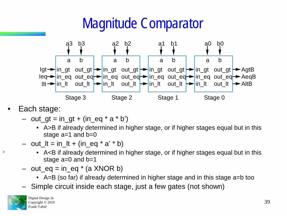
Magnitude Comparator
• Each stage:– out_gt = in_gt + (in_eq * a * b’)
• A>B if already determined in higher stage, or if higher stages equal but in this stage a=1 and b=0
– out_lt = in_lt + (in_eq * a’ * b)• A<B if already determined in higher stage, or if higher stages equal but in this
stage a=0 and b=1– out_eq = in_eq * (a XNOR b)
• A=B (so far) if already determined in higher stage and in this stage a=b too– Simple circuit inside each stage, just a few gates (not shown)
in_gtin_eqin_lt
out_gtout_eqout_lt
IgtIeqIlt
Stage 3
a3 b3
a bin_gtin_eqin_lt
out_gtout_eqout_lt
Stage 2
a2 b2
a bin_gtin_eqin_lt
out_gtout_eqout_lt
Stage 1
a1 b1
a bin_gtin_eqin_lt
out_gtout_eqout_lt
AgtBAeqBAltB
Stage 0
a0 b0
a b
a
Digital Design 2eCopyright © 2010Frank Vahid
40
Magnitude Comparator• How does it
work?
in_gtin_eqin_lt
out_gtout_eqout_lt
IgtIeqIlt
Stage3
a3 b3
a b
in_gtin_eqin_lt
out_gtout_eqout_lt
Stage2
a2 b2
a b
in_gtin_eqin_lt
out_gtout_eqout_lt
Stage1
a1 b1
a b
in_gtin_eqin_lt
out_gtout_eqout_lt
AgtBAeqBAltB
Stage0
a0 b01 1 0 0 1 0 1 1
a b
(a)
=
010
in_gtin_eqin_lt
out_gtout_eqout_lt
IgtIeqIlt
Stage3
a3 b3
a b
in_gtin_eqin_lt
out_gtout_eqout_lt
Stage2
a2 b2
a b
in_gtin_eqin_lt
out_gtout_eqout_lt
Stage1
a1 b1
a b
in_gtin_eqin_lt
out_gtout_eqout_lt
AgtBAeqBAltB
Stage0
a0 b01 1 0 0 1 0 1 1
a b
(b)
010
=
010
1011 = 1001 ?
010
Ieq=1 causes this stage to compare
a
010
Digital Design 2eCopyright © 2010Frank Vahid
41
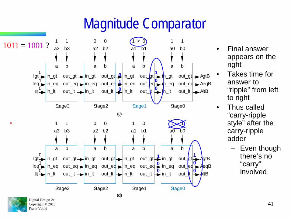
Magnitude Comparator• Final answer
appears on the right
• Takes time for answer to “ripple” from left to right
• Thus called “carry-ripple style” after the carry-ripple adder– Even though
there’s no “carry” involved
1011 = 1001 ?
in_gtin_eqin_lt
out_gtout_eqout_lt
IgtIeq
Ilt
Stage3
a3 b3
a b
in_gtin_eqin_lt
out_gtout_eqout_lt
Stage2
a2 b2
a b
in_gtin_eqin_lt
out_gtout_eqout_lt
Stage1
a1 b1
a b
in_gtin_eqin_lt
out_gtout_eqout_lt
AgtBAeqBAltB
Stage0
a0 b01 1 0 0 1 0 1 1
a b
(c)
0
10
1
00
>
in_gtin_eqin_lt
out_gtout_eqout_lt
IgtIeqIlt
Stage3
a3 b3
a b
in_gtin_eqin_lt
out_gtout_eqout_lt
Stage2
a2 b2
a b
in_gtin_eqin_lt
out_gtout_eqout_lt
Stage1
a1 b1
a b
in_gtin_eqin_lt
out_gtout_eqout_lt
AgtBAeqBAltB
Stage0
a0 b01 1 0 0 1 0 1 1
a b
(d)
0
10
01
0
a
010
100
Digital Design 2eCopyright © 2010Frank Vahid
42
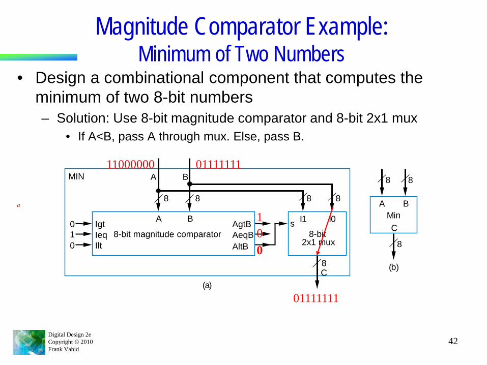
Magnitude Comparator Example: Minimum of Two Numbers
• Design a combinational component that computes the minimum of two 8-bit numbers– Solution: Use 8-bit magnitude comparator and 8-bit 2x1 mux
• If A<B, pass A through mux. Else, pass B.
MIN
IgtIeqIlt
AgtBAeqBAltB
010
A
A B
B
8-bit magnitude comparators I1 I0
2x1 mux8-bit
C
8
88 8 8
8
8
8
C
A BMin
(a)
(b)
11000000 01111111
001
01111111
a
Digital Design 2eCopyright © 2010Frank Vahid
43
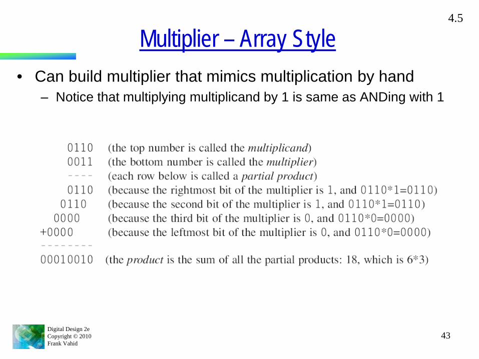
Multiplier – Array Style• Can build multiplier that mimics multiplication by hand
– Notice that multiplying multiplicand by 1 is same as ANDing with 1
4.5
Digital Design 2eCopyright © 2010Frank Vahid
44
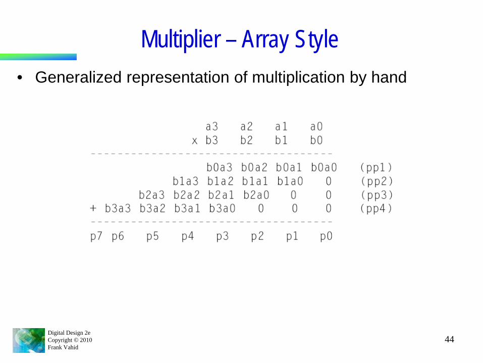
Multiplier – Array Style• Generalized representation of multiplication by hand
Digital Design 2eCopyright © 2010Frank Vahid
45
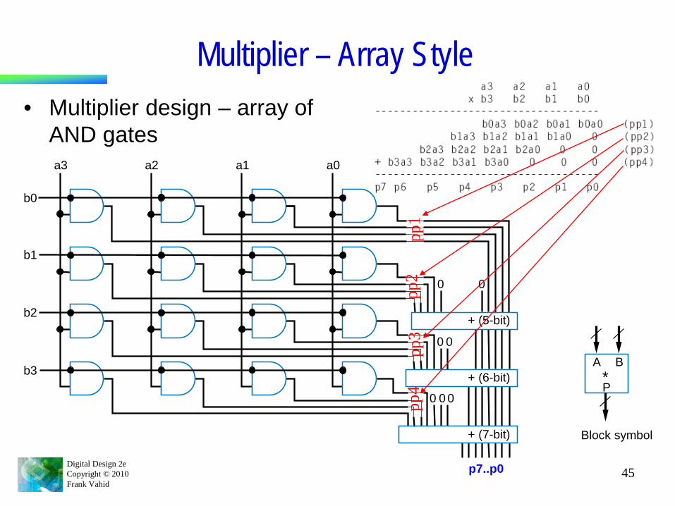
Multiplier – Array Style• Multiplier design – array of
AND gates
A B
P*
Block symbol
+ (5-bit)
+ (6-bit)
+ (7-bit)
0 0
0 0 0
0
a0a1a2a3
b0
b1
b2
b3
0
p7..p0
pp1
pp2
pp3
pp4
Digital Design 2eCopyright © 2010Frank Vahid
46
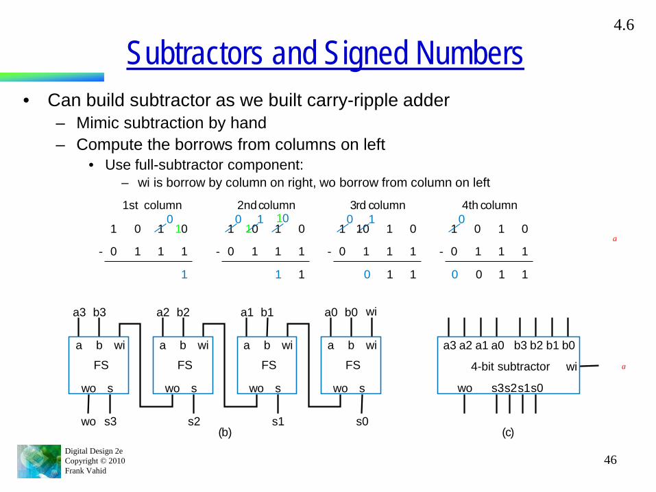
0
Subtractors and Signed Numbers• Can build subtractor as we built carry-ripple adder
– Mimic subtraction by hand– Compute the borrows from columns on left
• Use full-subtractor component: – wi is borrow by column on right, wo borrow from column on left
4.6
1 1 00
0 1 1
1
1
10
-
1st column
1 1 010
0
0 1 1
10 1
1-
3rd column
1 1 00
0
0 1 1
100 1
1-
4th column
wo
a3
a b
FS
wi
wo s
b3
s3
a2
a b
FS
wi
wo s
b2
s2
a1
a b
FS
wi
wo s
b1
s1
a0
a b
FS
wi
wi
wo s
b0
s0(b)
a3 a2 a1 a0 b3
s3s2s1s0wo
wi
b2 b1 b0
(c)
4-bit subtractor a
1 1 0
0 1 1
1 1
1
10
-
2ndcolumn10
1 1a
Digital Design 2eCopyright © 2010Frank Vahid
47
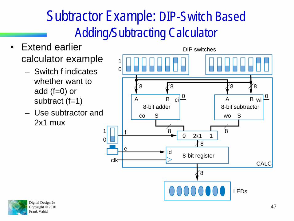
Subtractor Example: DIP-Switch Based Adding/Subtracting Calculator
• Extend earlier calculator example– Switch f indicates
whether want to add (f=0) or subtract (f=1)
– Use subtractor and 2x1 mux
DIP switches
10
8-bit registerCALC
LEDs
e
f
clkld
8
8
8
0 0
8
8
8
882x10 1
10
wiciA AB B
S Sco wo8-bit adder 8-bit subtractor
Digital Design 2eCopyright © 2010Frank Vahid
48
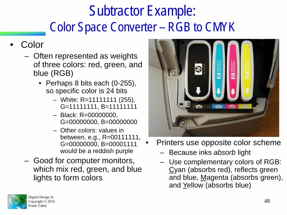
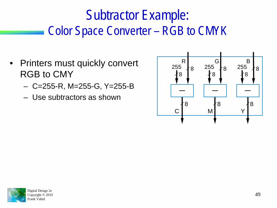
Subtractor Example: Color Space Converter – RGB to CMYK
• Color– Often represented as weights
of three colors: red, green, and blue (RGB)
• Perhaps 8 bits each (0-255), so specific color is 24 bits
– White: R=11111111 (255), G=11111111, B=11111111
– Black: R=00000000, G=00000000, B=00000000
– Other colors: values in between, e.g., R=00111111, G=00000000, B=00001111 would be a reddish purple
– Good for computer monitors, which mix red, green, and blue lights to form colors
• Printers use opposite color scheme– Because inks absorb light– Use complementary colors of RGB:
Cyan (absorbs red), reflects green and blue, Magenta (absorbs green), and Yellow (absorbs blue)
Digital Design 2eCopyright © 2010Frank Vahid
49
Subtractor Example: Color Space Converter – RGB to CMYK
• Printers must quickly convert RGB to CMY – C=255-R, M=255-G, Y=255-B– Use subtractors as shown
— — —
R G B8
88888
8 8 8
255 255 255
C M Y
Digital Design 2eCopyright © 2010Frank Vahid
50
Subtractor Example: Color Space Converter – RGB to CMYK
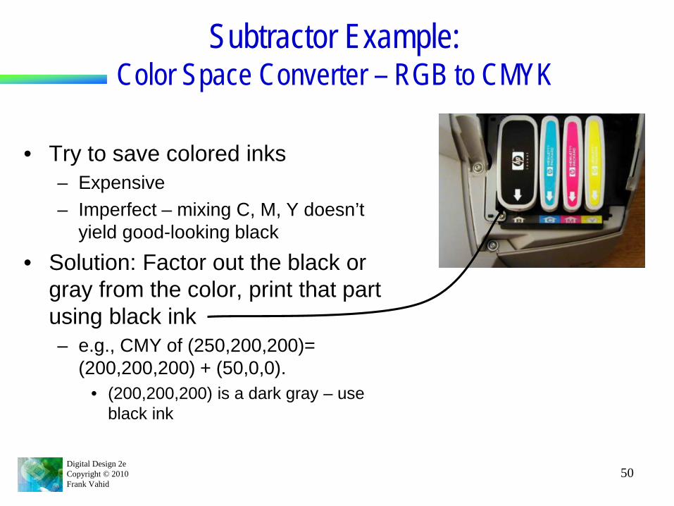
• Try to save colored inks– Expensive– Imperfect – mixing C, M, Y doesn’t
yield good-looking black
• Solution: Factor out the black or gray from the color, print that part using black ink– e.g., CMY of (250,200,200)=
(200,200,200) + (50,0,0).• (200,200,200) is a dark gray – use
black ink
Digital Design 2eCopyright © 2010Frank Vahid
51
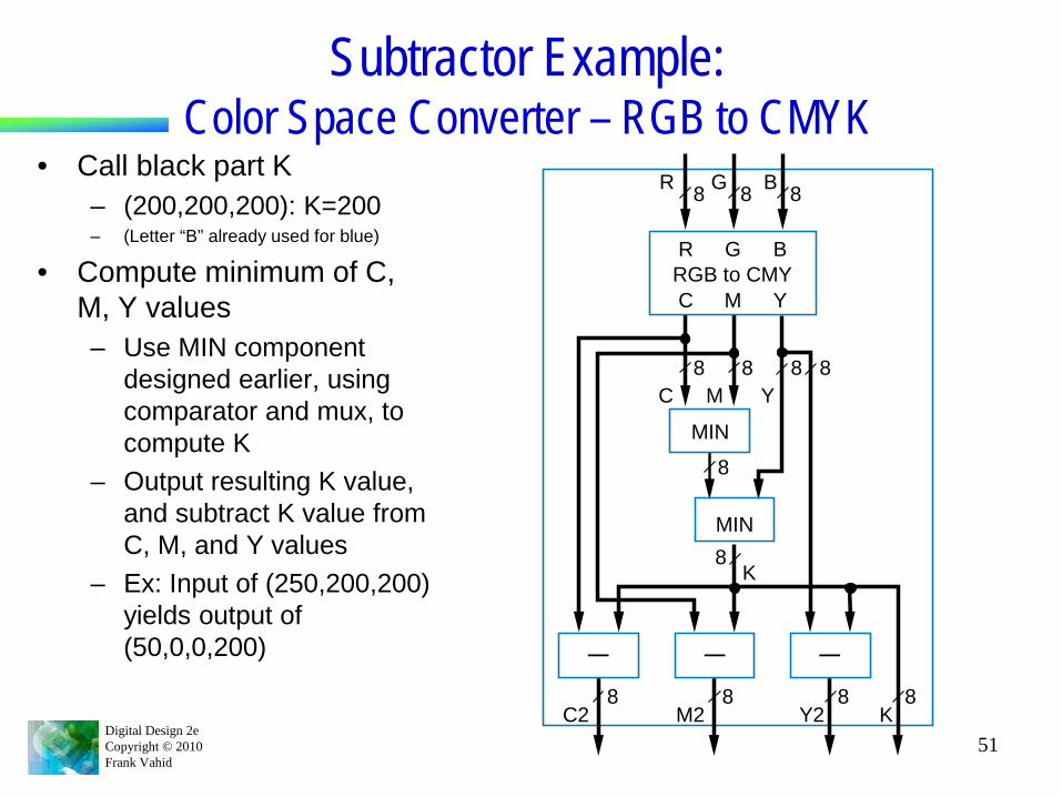
Subtractor Example: Color Space Converter – RGB to CMYK
• Call black part K– (200,200,200): K=200– (Letter “B” already used for blue)
• Compute minimum of C, M, Y values– Use MIN component
designed earlier, using comparator and mux, to compute K
– Output resulting K value, and subtract K value from C, M, and Y values
– Ex: Input of (250,200,200) yields output of (50,0,0,200) — — —
8 8C2 M2 Y2 K
8
8
888 8
8 8
MIN
MIN
C
C M Y
R GRGB to CMY
B
M Y
K
R G B8 8 8
Digital Design 2eCopyright © 2010Frank Vahid
52
Representing Negative Numbers: Two’s Complement
• Negative numbers common– How represent in binary?
• Signed-magnitude– Use leftmost bit for sign bit
• So -5 would be:1101 using four bits10000101 using eight bits
• Better way: Two’s complement– Big advantage: Allows us to perform subtraction using addition– Thus, only need adder component, no need for separate
subtractor component
Digital Design 2eCopyright © 2010Frank Vahid
53
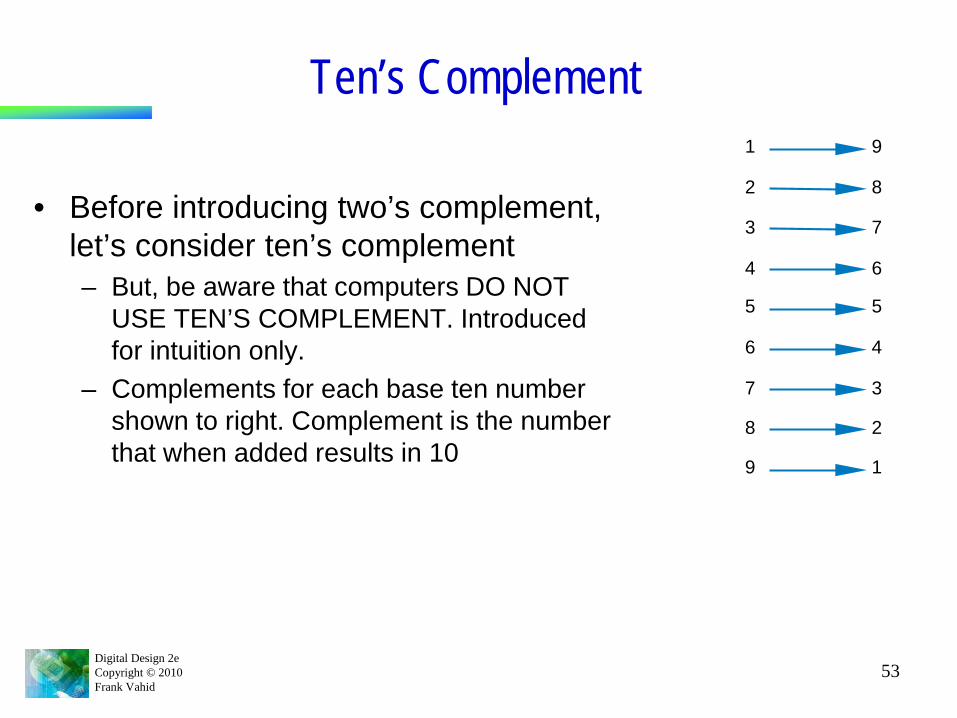
Ten’s Complement
• Before introducing two’s complement, let’s consider ten’s complement– But, be aware that computers DO NOT
USE TEN’S COMPLEMENT. Introduced for intuition only.
– Complements for each base ten number shown to right. Complement is the number that when added results in 10
9
8
7
6
5
4
3
2
1
1
2
3
4
5
6
7
8
9
Digital Design 2eCopyright © 2010Frank Vahid
54
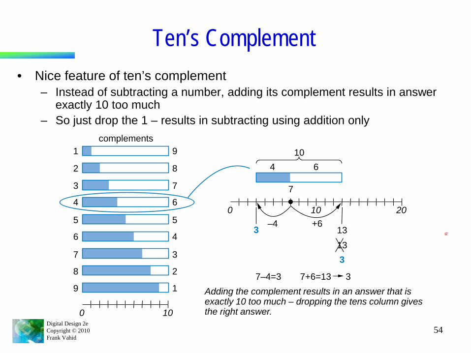
Ten’s Complement• Nice feature of ten’s complement
– Instead of subtracting a number, adding its complement results in answer exactly 10 too much
– So just drop the 1 – results in subtracting using addition only
4 610
7
–4 +60 10 20
3 13133
0 10
1
2
3
4
5
6
7
8
9
9
8
7
6
5
4
3
2
1
complements
7–4=3 7+6=13 3Adding the complement results in an answer that isexactly 10 too much – dropping the tens column givesthe right answer.
a
Digital Design 2eCopyright © 2010Frank Vahid
55
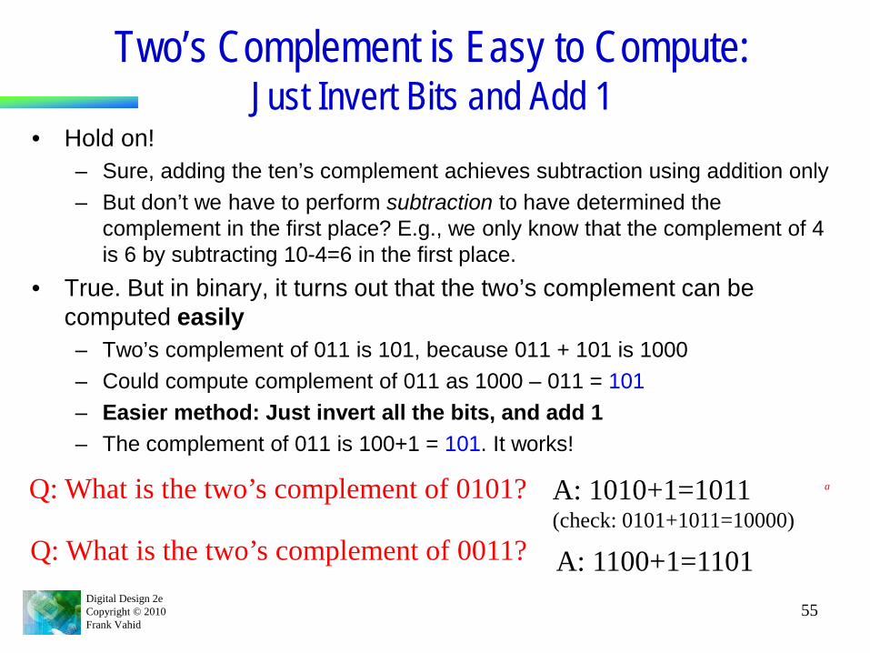
Two’s Complement is Easy to Compute: Just Invert Bits and Add 1
• Hold on!– Sure, adding the ten’s complement achieves subtraction using addition only– But don’t we have to perform subtraction to have determined the
complement in the first place? E.g., we only know that the complement of 4 is 6 by subtracting 10-4=6 in the first place.
• True. But in binary, it turns out that the two’s complement can be computed easily– Two’s complement of 011 is 101, because 011 + 101 is 1000– Could compute complement of 011 as 1000 – 011 = 101– Easier method: Just invert all the bits, and add 1– The complement of 011 is 100+1 = 101. It works!
Q: What is the two’s complement of 0101? A: 1010+1=1011(check: 0101+1011=10000)
a
Q: What is the two’s complement of 0011? A: 1100+1=1101
Digital Design 2eCopyright © 2010Frank Vahid
56
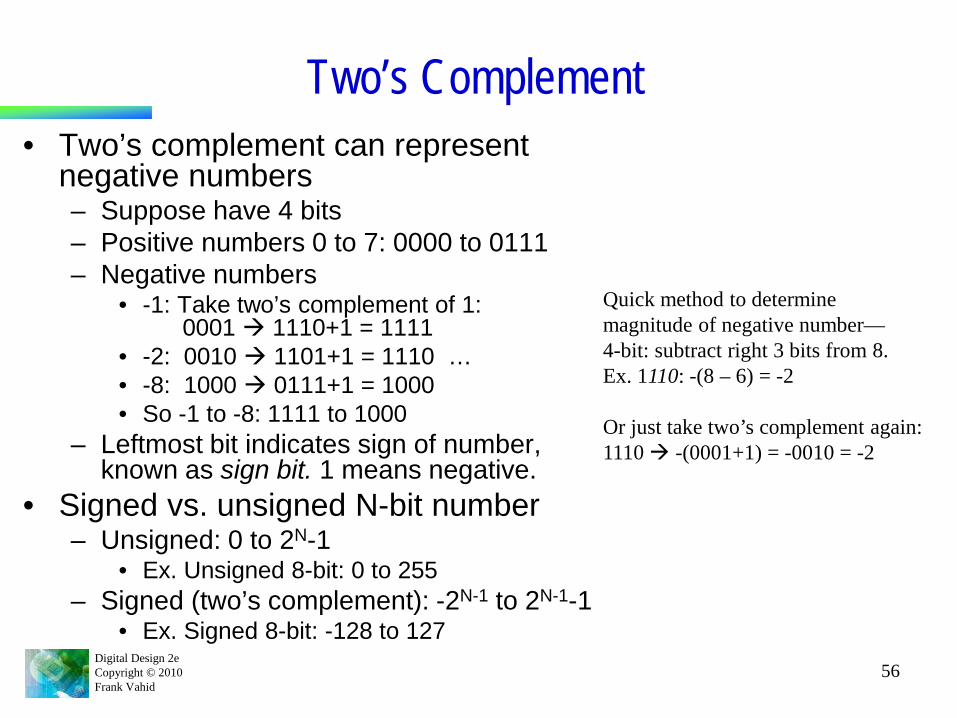
Two’s Complement• Two’s complement can represent
negative numbers– Suppose have 4 bits– Positive numbers 0 to 7: 0000 to 0111– Negative numbers
• -1: Take two’s complement of 1: 0001 1110+1 = 1111
• -2: 0010 1101+1 = 1110 …• -8: 1000 0111+1 = 1000• So -1 to -8: 1111 to 1000
– Leftmost bit indicates sign of number, known as sign bit. 1 means negative.
• Signed vs. unsigned N-bit number– Unsigned: 0 to 2N-1
• Ex. Unsigned 8-bit: 0 to 255– Signed (two’s complement): -2N-1 to 2N-1-1
• Ex. Signed 8-bit: -128 to 127
Quick method to determine magnitude of negative number—4-bit: subtract right 3 bits from 8. Ex. 1110: -(8 – 6) = -2
Or just take two’s complement again: 1110 -(0001+1) = -0010 = -2
Digital Design 2eCopyright © 2010Frank Vahid
57
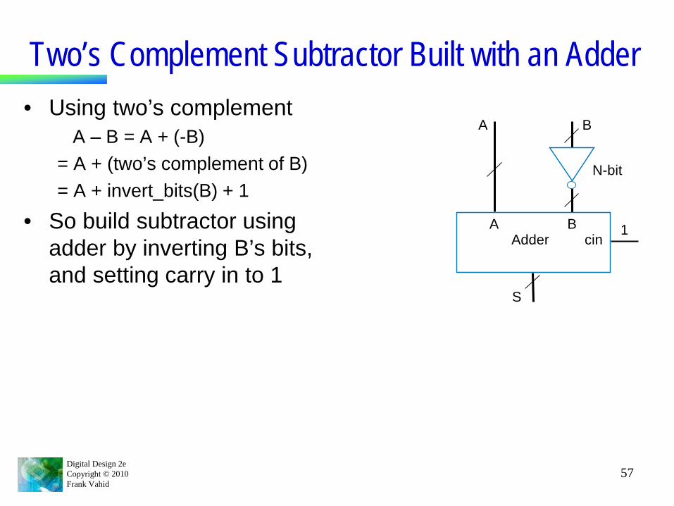
Two’s Complement Subtractor Built with an Adder• Using two’s complement
A – B = A + (-B) = A + (two’s complement of B) = A + invert_bits(B) + 1
• So build subtractor using adder by inverting B’s bits, and setting carry in to 1
1cin
BAAdder
S
BA
N-bit
Digital Design 2eCopyright © 2010Frank Vahid
58
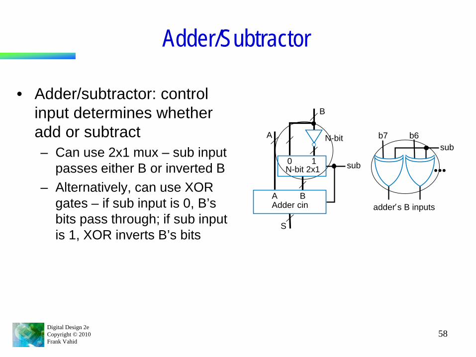
Adder/Subtractor
• Adder/subtractor: control input determines whether add or subtract– Can use 2x1 mux – sub input
passes either B or inverted B– Alternatively, can use XOR
gates – if sub input is 0, B’s bits pass through; if sub input is 1, XOR inverts B’s bits
b7 b6sub
adder′s B inputs
0 1N-bit 2x1
N-bitA
A
S
B
B
sub
Adder cin

Digital Design 2eCopyright © 2010Frank Vahid
59
Adder/Subtractor Example: Calculator• Previous calculator
used separate adder and subtractor
• Improve by using adder/subtractor, and two’s complement numbers
DIP switches
10
8-bit register
8-bit adder/subtractorsub
CALC
LEDs
e
S
A Bf
clkld
10
8 8
8
8
DIP switches10
8-bit registerCALC
LEDs
e
f
clkld
8
8
80 0
8
8
8
88 2x10 110
wiciA AB B
S Sco wo8-bit adder 8-bit subtractor
Digital Design 2eCopyright © 2010Frank Vahid
60
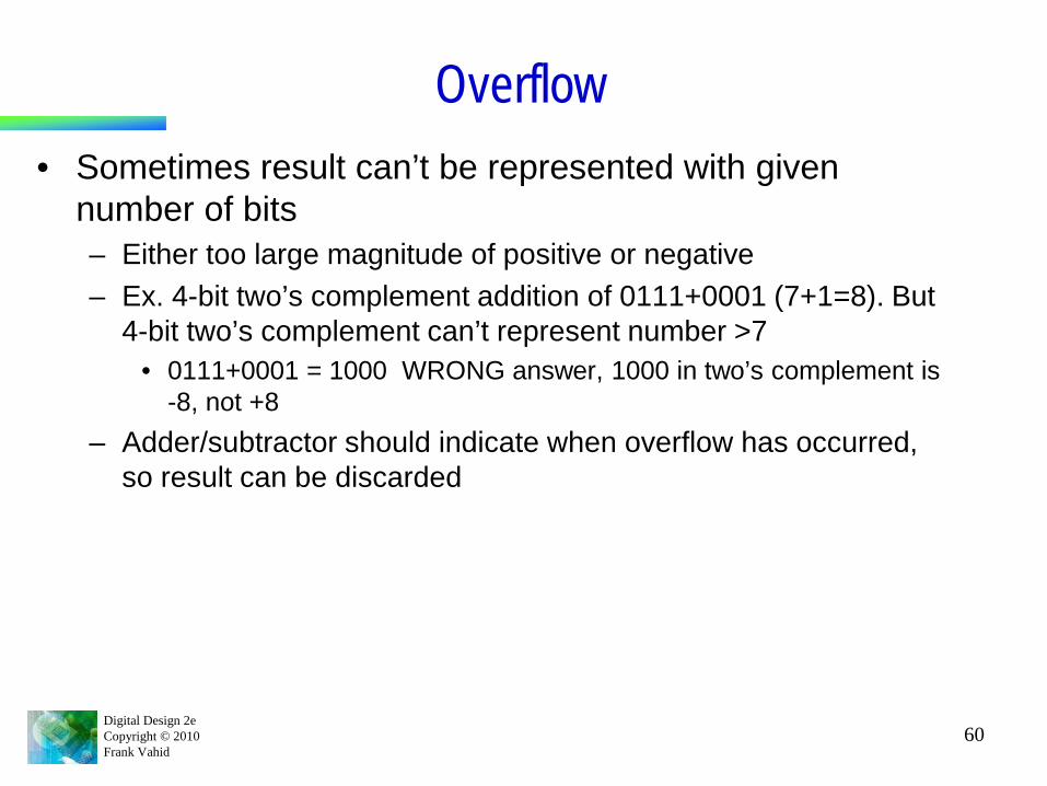
Overflow• Sometimes result can’t be represented with given
number of bits– Either too large magnitude of positive or negative– Ex. 4-bit two’s complement addition of 0111+0001 (7+1=8). But
4-bit two’s complement can’t represent number >7• 0111+0001 = 1000 WRONG answer, 1000 in two’s complement is
-8, not +8– Adder/subtractor should indicate when overflow has occurred,
so result can be discarded
Digital Design 2eCopyright © 2010Frank Vahid
61
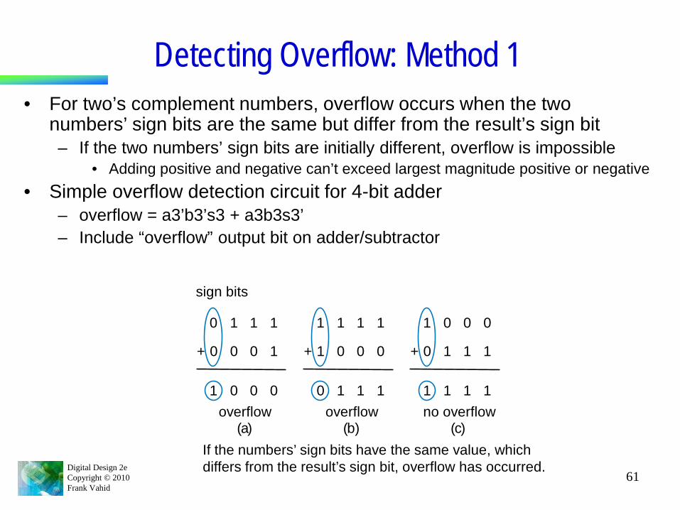
Detecting Overflow: Method 1• For two’s complement numbers, overflow occurs when the two
numbers’ sign bits are the same but differ from the result’s sign bit– If the two numbers’ sign bits are initially different, overflow is impossible
• Adding positive and negative can’t exceed largest magnitude positive or negative• Simple overflow detection circuit for 4-bit adder
– overflow = a3’b3’s3 + a3b3s3’– Include “overflow” output bit on adder/subtractor
0 1 1 1
1 0 0 0
+ 00 0 1
sign bits
overflow(a)
1 1 1 1
0 1 1 1
+ 01 0 0
overflow(b)
1 0 0 0
1 1 1 1
+ 10 1 1
no overflow(c)
If the numbers’ sign bits have the same value, whichdiffers from the result’s sign bit, overflow has occurred.
Digital Design 2eCopyright © 2010Frank Vahid
62
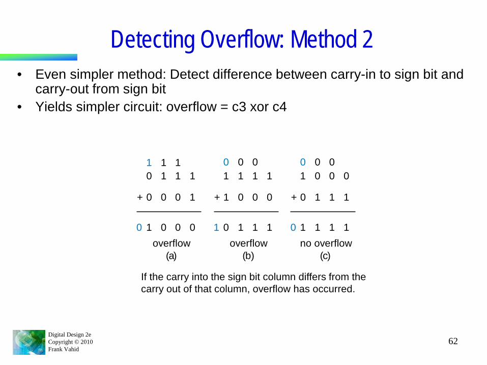
Detecting Overflow: Method 2• Even simpler method: Detect difference between carry-in to sign bit and
carry-out from sign bit• Yields simpler circuit: overflow = c3 xor c4
0 1 11 1 1
1
10 010 0 0
+ 00 0 1
overflow(a)
1 1 10 0 0
1
0 1 1 1
+ 01 0 0
overflow(b)
1 0 00 0 0
0
1 1 1 1
+ 10 1 1
no overflow(c)
If the carry into the sign bit column differs from thecarry out of that column, overflow has occurred.
Digital Design 2eCopyright © 2010Frank Vahid
63
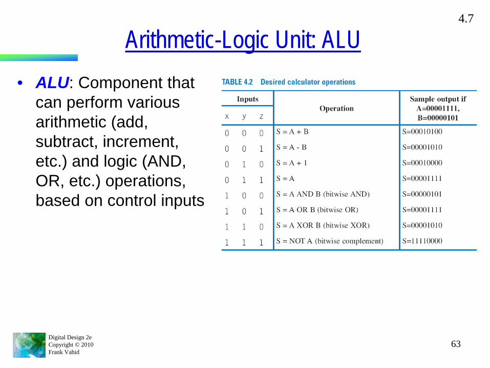
Arithmetic-Logic Unit: ALU• ALU: Component that
can perform various arithmetic (add, subtract, increment, etc.) and logic (AND, OR, etc.) operations, based on control inputs
4.7
Digital Design 2eCopyright © 2010Frank Vahid
64
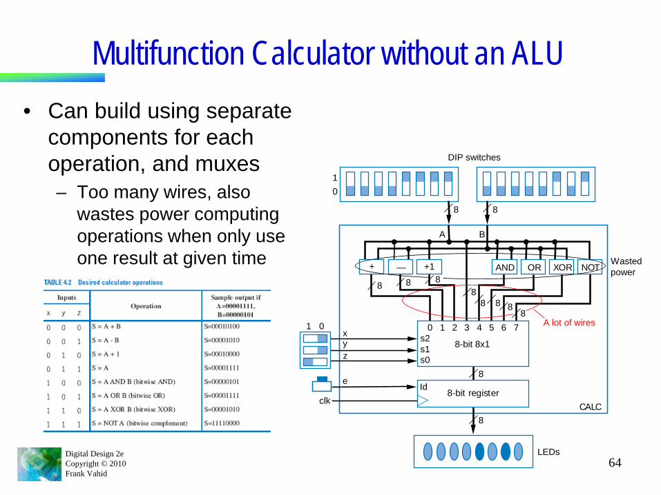
Multifunction Calculator without an ALU• Can build using separate
components for each operation, and muxes– Too many wires, also
wastes power computing operations when only use one result at given time
DIP switches
10
8-bit register
8-bit 8x1
CALC
LEDs
e
zyx
clkId
s0s1s2
1 0 0 1 2 3 4 5 6 7
NOTXORORAND+1+
8 8
88
8
8
8
8 88
88
A B
A lot of wires
Wastedpower—

Digital Design 2eCopyright © 2010Frank Vahid
65
ALU• More efficient design uses ALU
– ALU design not just separate components multiplexed (same problem as previous slide)
– Instead, ALU design uses single adder, plus logic in front of adder’s A and B inputs• Logic in front is called an arithmetic-logic extender
– Extender modifies A and B inputs so desired operation appears at output of the adder
(a)
ALU
IA IB
ISAdder cin
A B
S
xyz
AL-extender
abext abext abext cinext
AL-extender
ia7 ib7
a7 b7
ia6 ib6
a6 b6
ia0 ib0
a0 b0
cin(b)
xyz
a
Digital Design 2eCopyright © 2010Frank Vahid
66
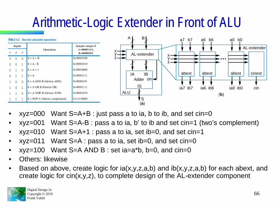
Arithmetic-Logic Extender in Front of ALU
• xyz=000 Want S=A+B : just pass a to ia, b to ib, and set cin=0• xyz=001 Want S=A-B : pass a to ia, b’ to ib and set cin=1 (two’s complement)• xyz=010 Want S=A+1 : pass a to ia, set ib=0, and set cin=1• xyz=011 Want S=A : pass a to ia, set ib=0, and set cin=0• xyz=100 Want S=A AND B : set ia=a*b, b=0, and cin=0• Others: likewise• Based on above, create logic for ia(x,y,z,a,b) and ib(x,y,z,a,b) for each abext, and
create logic for cin(x,y,z), to complete design of the AL-extender component
abext abext abext cinext
xyz
AL-extender
ia7 ib7
a7 b7
ia6 ib6
a6 b6
ia0 ib0
a0 b0
cin(b)
(a)
ALU
IA IB
ISAdder cin
A B
AL-extender
S
xyz
Digital Design 2eCopyright © 2010Frank Vahid
67
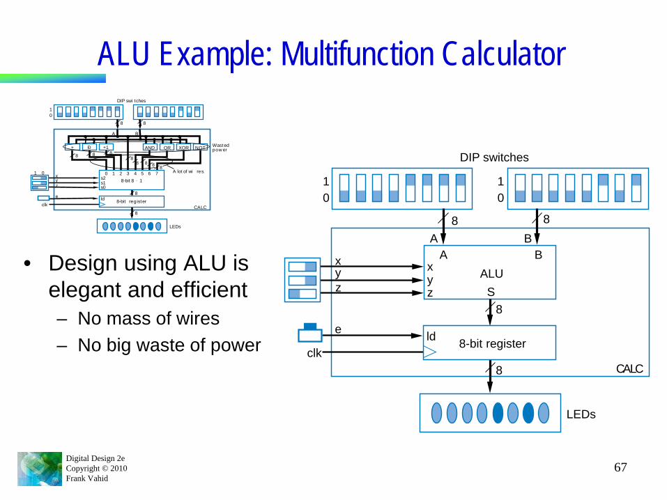
ALU Example: Multifunction Calculator
• Design using ALU is elegant and efficient– No mass of wires– No big waste of power
DIP switches
10
10
8-bit register
ALUS
CALC
LEDs
e
zyx
clkld
zyx
8
8
8
8A
AB
B
DIP swi tches
10
8-bit reg ister
8-bit 8 ⋅ 1
CALC
LEDs
e
zyx
clkId
s0s1s2
1 0 0 1 2 3 4 5 6 7
NOTXORORAND+1Ð+
8 8
88
8
8
8
8 8 8
88
A B
A lot of wi res.
Wast edpow er
Digital Design 2eCopyright © 2010Frank Vahid
68
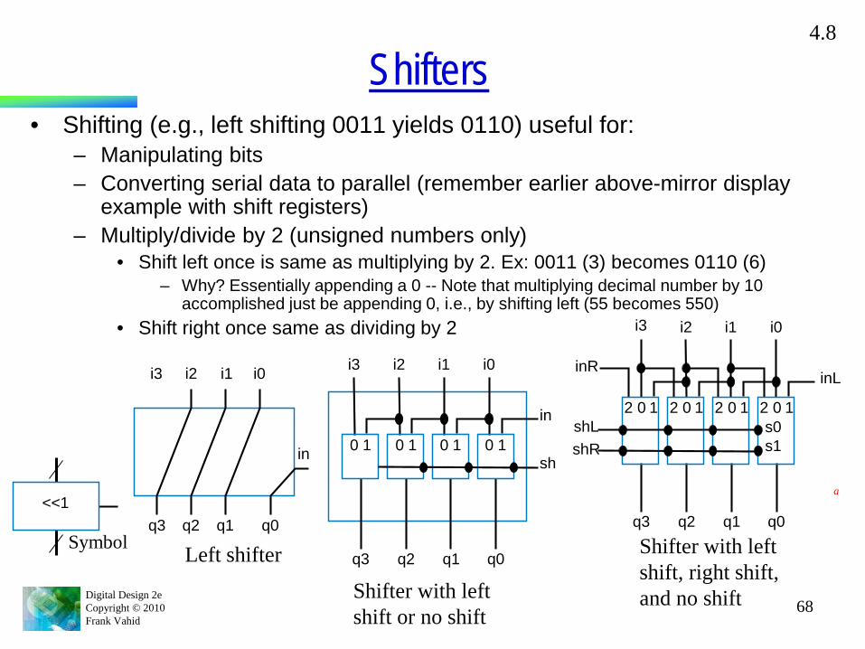
Shifters• Shifting (e.g., left shifting 0011 yields 0110) useful for:
– Manipulating bits– Converting serial data to parallel (remember earlier above-mirror display
example with shift registers)– Multiply/divide by 2 (unsigned numbers only)
• Shift left once is same as multiplying by 2. Ex: 0011 (3) becomes 0110 (6)– Why? Essentially appending a 0 -- Note that multiplying decimal number by 10
accomplished just be appending 0, i.e., by shifting left (55 becomes 550)• Shift right once same as dividing by 2
i2
q3 q2 q1 q0
in
i3 i1 i0
Left shifter
0 1 0 1 0 1 0 1
in
sh
i3
q3 q2 q1 q0
i2 i1 i0
Shifter with left shift or no shift
inL
i3
q3 q2 q1 q0
i2 i1 i0
inR
2 0s0s1
shLshR
1 2 0 1 2 0 1 2 0 1
Shifter with left shift, right shift, and no shift
<<1
Symbol
4.8
a
Digital Design 2eCopyright © 2010Frank Vahid
69
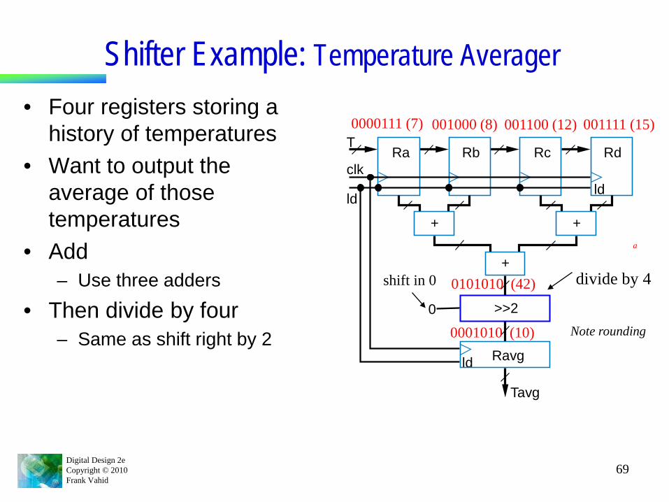
Shifter Example: Temperature Averager• Four registers storing a
history of temperatures• Want to output the
average of those temperatures
• Add – Use three adders
• Then divide by four– Same as shift right by 2
Tavg
Ravgld
ld
T
clk
ld
Ra Rb Rc Rd
+ +
+
>>20
divide by 4shift in 0
a
001000 (8) 001100 (12) 001111 (15)0000111 (7)
0101010 (42)
0001010 (10) Note rounding
Digital Design 2eCopyright © 2010Frank Vahid
70
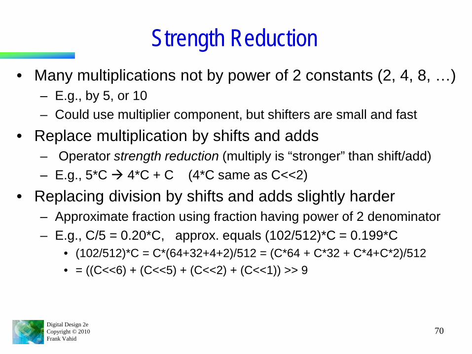
Strength Reduction• Many multiplications not by power of 2 constants (2, 4, 8, …)
– E.g., by 5, or 10– Could use multiplier component, but shifters are small and fast
• Replace multiplication by shifts and adds– Operator strength reduction (multiply is “stronger” than shift/add)– E.g., 5*C 4*C + C (4*C same as C<<2)
• Replacing division by shifts and adds slightly harder– Approximate fraction using fraction having power of 2 denominator– E.g., C/5 = 0.20*C, approx. equals (102/512)*C = 0.199*C
• (102/512)*C = C*(64+32+4+2)/512 = (C*64 + C*32 + C*4+C*2)/512• = ((C<<6) + (C<<5) + (C<<2) + (C<<1)) >> 9
Digital Design 2eCopyright © 2010Frank Vahid
71
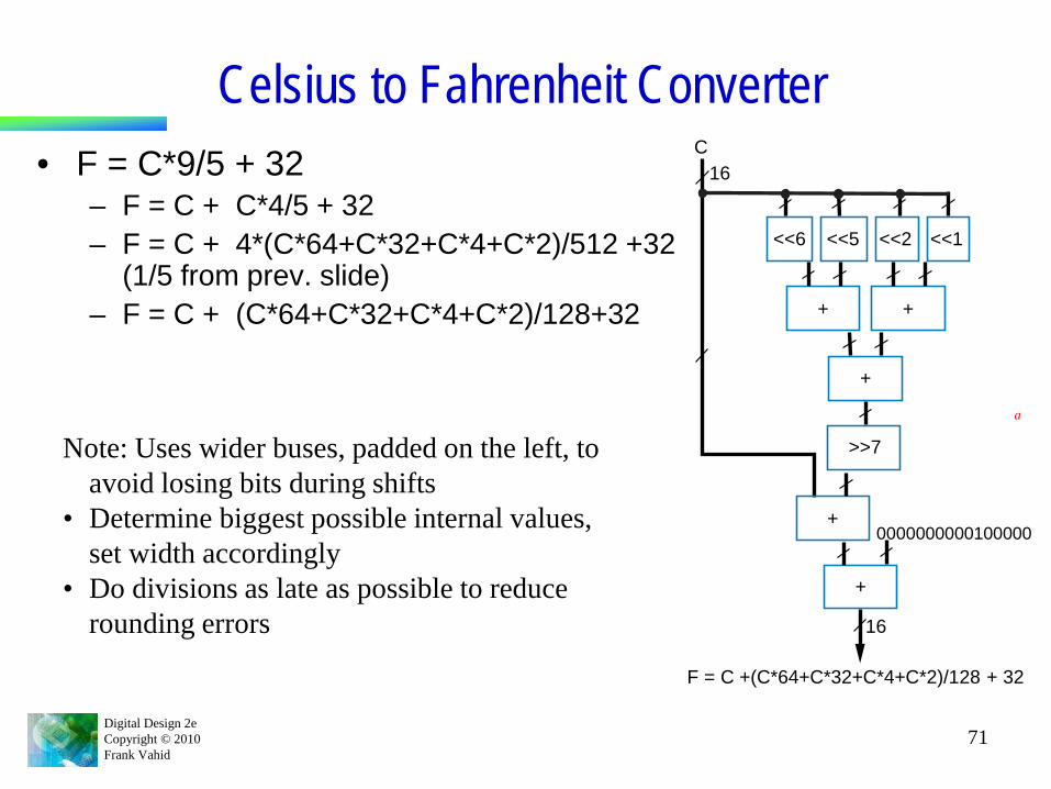
Celsius to Fahrenheit Converter• F = C*9/5 + 32
– F = C + C*4/5 + 32– F = C + 4*(C*64+C*32+C*4+C*2)/512 +32
(1/5 from prev. slide)– F = C + (C*64+C*32+C*4+C*2)/128+32
>>7
C16
16
0000000000100000
F = C +(C*64+C*32+C*4+C*2)/128 + 32
+
+ +
<<6 <<5 <<2 <<1
+
+
a
Note: Uses wider buses, padded on the left, to avoid losing bits during shifts
• Determine biggest possible internal values, set width accordingly
• Do divisions as late as possible to reduce rounding errors
Digital Design 2eCopyright © 2010Frank Vahid
72
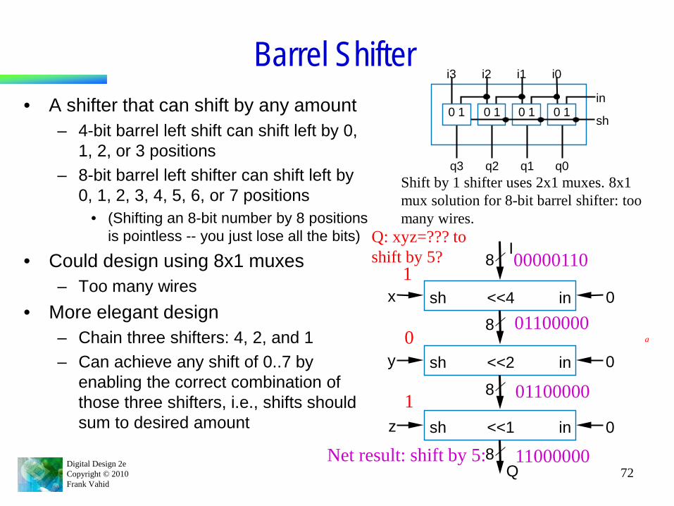
Barrel Shifter• A shifter that can shift by any amount
– 4-bit barrel left shift can shift left by 0, 1, 2, or 3 positions
– 8-bit barrel left shifter can shift left by 0, 1, 2, 3, 4, 5, 6, or 7 positions
• (Shifting an 8-bit number by 8 positions is pointless -- you just lose all the bits)
• Could design using 8x1 muxes– Too many wires
• More elegant design– Chain three shifters: 4, 2, and 1– Can achieve any shift of 0..7 by
enabling the correct combination of those three shifters, i.e., shifts should sum to desired amount
0 1 0 1 0 1 0 1in
sh
i3
q3 q2 q1 q0
i2 i1 i0
Shift by 1 shifter uses 2x1 muxes. 8x1 mux solution for 8-bit barrel shifter: too many wires.
<<1 insh
0
0
0
x
y
z
8Q
<<2 insh
8
<<4 insh
8
8I
Q: xyz=??? to shift by 5?
a
1
0
1
00000110
01100000
01100000
11000000Net result: shift by 5:
Digital Design 2eCopyright © 2010Frank Vahid
73
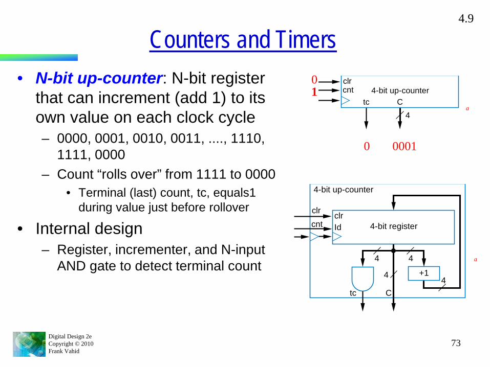
Counters and Timers• N-bit up-counter: N-bit register
that can increment (add 1) to its own value on each clock cycle– 0000, 0001, 0010, 0011, ...., 1110,
1111, 0000– Count “rolls over” from 1111 to 0000
• Terminal (last) count, tc, equals1 during value just before rollover
• Internal design– Register, incrementer, and N-input
AND gate to detect terminal count
4.9
0000
01
00010010001101000101...11100 111110 00000001
a
a
cnttc C
4-bit up-counter
4
clr0
Id 4-bit register
Ctc
4
4 4
4
cnt
4-bit up-counter
+1
clrclr
Digital Design 2eCopyright © 2010Frank Vahid
74
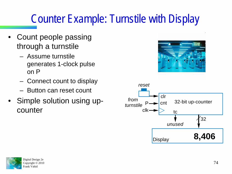
Counter Example: Turnstile with Display• Count people passing
through a turnstile– Assume turnstile
generates 1-clock pulse on P
– Connect count to display– Button can reset count
• Simple solution using up-counter
32-bit up-countercnt
tc
Display
unused
Pclk
clr
32
8,406
fromturnstile
reset
Digital Design 2eCopyright © 2010Frank Vahid
75
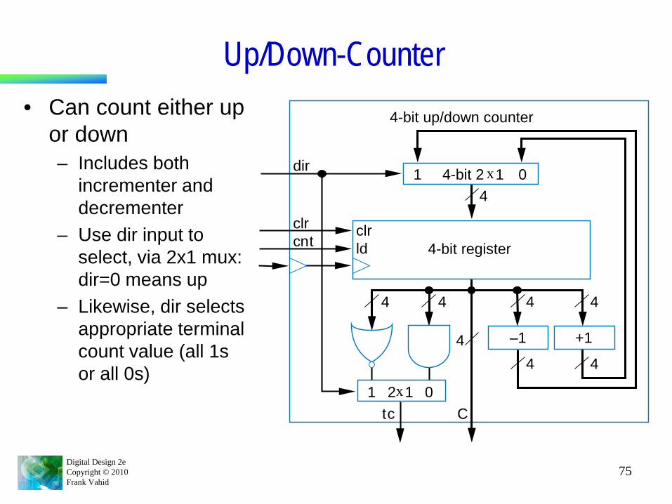
Up/Down-Counter• Can count either up
or down– Includes both
incrementer and decrementer
– Use dir input to select, via 2x1 mux: dir=0 means up
– Likewise, dir selects appropriate terminal count value (all 1s or all 0s)
ld 4-bit register
Ctc
4
44 44
4
cntclrclr
dir
4-bit up/down counter
4 4
–1 +1
1 02x1
1 04-bit 2 x1
Digital Design 2eCopyright © 2010Frank Vahid
76
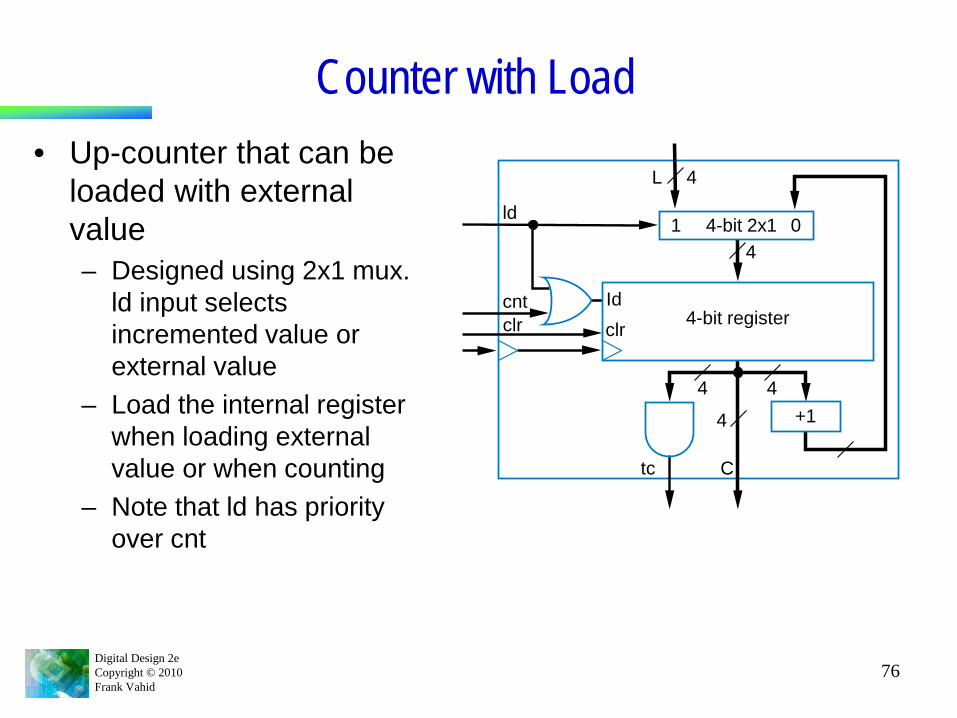
Counter with Load• Up-counter that can be
loaded with external value– Designed using 2x1 mux.
ld input selects incremented value or external value
– Load the internal register when loading external value or when counting
– Note that ld has priority over cnt
Id4-bit register
Ctc
4
4 4
cnt
ld
+1
1 04-bit 2x1
L 4
4
clrclr
Digital Design 2eCopyright © 2010Frank Vahid
77
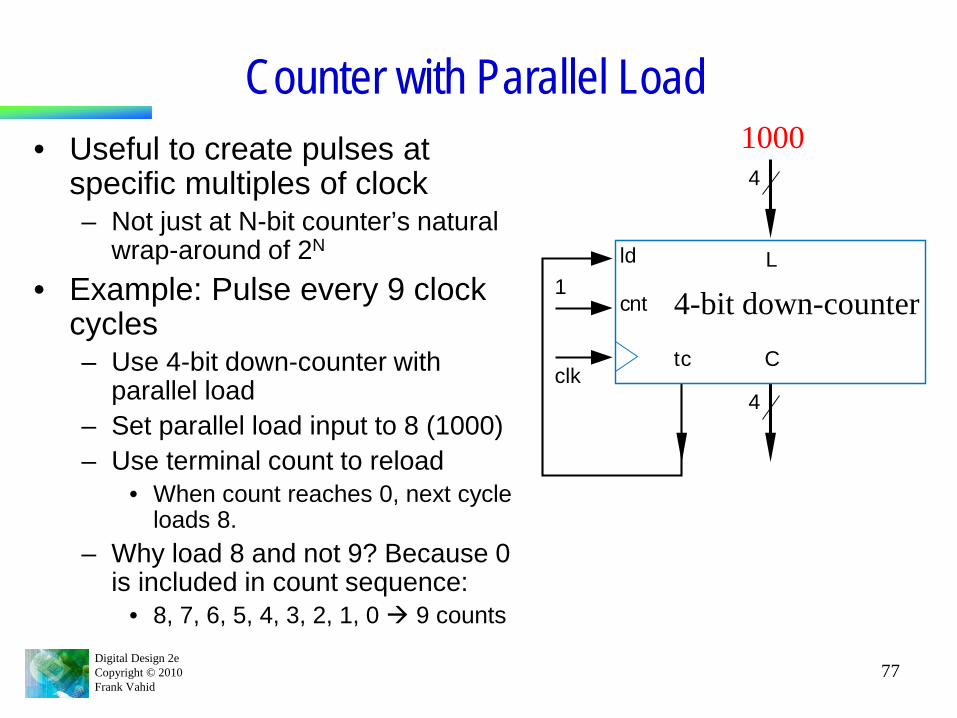
Counter with Parallel Load• Useful to create pulses at
specific multiples of clock– Not just at N-bit counter’s natural
wrap-around of 2N
• Example: Pulse every 9 clock cycles– Use 4-bit down-counter with
parallel load– Set parallel load input to 8 (1000)– Use terminal count to reload
• When count reaches 0, next cycle loads 8.
– Why load 8 and not 9? Because 0 is included in count sequence:
• 8, 7, 6, 5, 4, 3, 2, 1, 0 9 counts
cnt
ld
tc C
L1
clk4
4
1000
4-bit down-counter
Digital Design 2eCopyright © 2010Frank Vahid
78
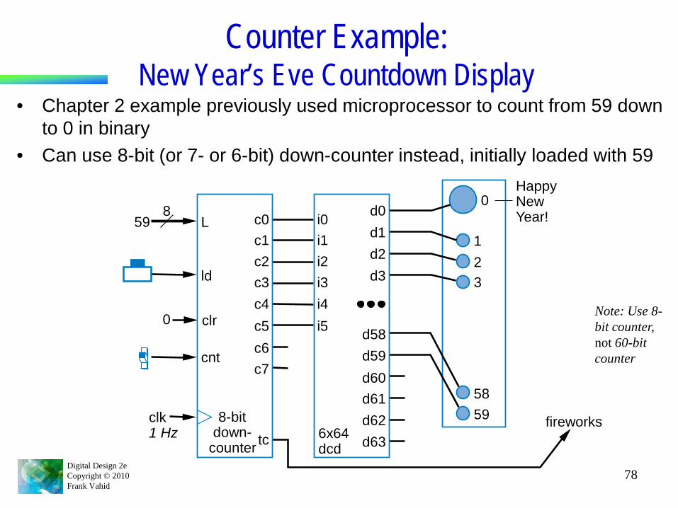
Counter Example: New Year’s Eve Countdown Display
• Chapter 2 example previously used microprocessor to count from 59 down to 0 in binary
• Can use 8-bit (or 7- or 6-bit) down-counter instead, initially loaded with 59
d0i0i1i2i3i4i5
c0c1c2c3c4c5c6c7
tc
d1d2d3
d58d59d60d61d62d636x64
dcd
8-bitdown-
counter
598
L
ld
cnt
clk1 Hz
fireworks
HappyNewYear!
0
123
5859
clr0 Note: Use 8-bit counter, not 60-bit counter
Digital Design 2eCopyright © 2010Frank Vahid
79
Common Counter Use: Clock Divider• Suppose have 512 Hz
oscillator, but want 2 Hz pulse– Thus, want divide fast clock
by 256– Design using 8-bit up-
counter, use tc output as pulse
• Counts from 0 to 255 (256 counts), so pulses tc every 256 cycles
cnttc C
(unused)
8-bit up-counter1
osc512 MHz 8
p2 MHz
Digital Design 2eCopyright © 2010Frank Vahid
80
Clock Division by Amount not Power of 2 Example: 1 Hz Pulse Generator from 60 Hz Clock
• Example: U.S. electricity standard uses 60 Hz signal– Device may convert that to 1 Hz signal to count seconds
• Use 6-bit up-counter– Up counter: Detected count of 59 clears counter to 0; tc thus pulses every 60
cycles• Note: Detect 59, not 60 (because the first number, 0, is included)
– Down counter approach also possible: When count reaches 0, load 59
Ctc
p
1osc
60 Hz
1 Hz
clrcnt 6-bit up-counter
Ctc
p
1
osc60 Hz
1 Hz
ldcnt 6-bit down-counter
unused
1 01 1 11
Digital Design 2eCopyright © 2010Frank Vahid
81
Measuring Time Between Events using an Up-Counter• Initially clear to 0. 1st event: Set cnt=1. 2nd event: Set cnt=0.
– Then, multiply counted clock cycles by clock period to determine time• Ex: Highway speed measurement system
– Two sensors “a” and “b” in road– Use FSM to detect “a” becoming 1, set cnt=1. Set cnt=0 when “b” 1– If clock is 1 kHz (period is 1 ms), then time is C * 0.001s
• If a and b separated by 0.01 miles, then vehicle speed in mph is: 0.01 miles / (time * (1 hour / 3600 seconds))
• E.g., if C is 500, then speed is 0.01 / ((500*0.001) / 3600) = 72 mph
S0 S1
clr=1 cnt=1 cnt=0(compute time
and outputspeed)
S2a b
a’ b’
vehicle
SpeedMeasurer s
16C
a
b
clrcnt
SpeedMeasurer
Digital Design 2eCopyright © 2010Frank Vahid
82
Timers• Pulses output at user-
specified timer interval when enabled– “Ticks” like a clock– Interval specified as multiple of
base time unit– If base is 1 microsec and user
wants pulse every 300 ms, loads 300,000 into timer
• Can design using oscillator, register, and down-counter
(b)
Q loadenable
Q
32-bit1-microsec
timer
(c)
32
M
Ctc
Q
1 microsecoscillator
ld32-bit
down-counter
(a)
unused
enable cnt
ldload
32
M
32-bit register
1 04-bit 2x1
-1
Digital Design 2eCopyright © 2010Frank Vahid
83
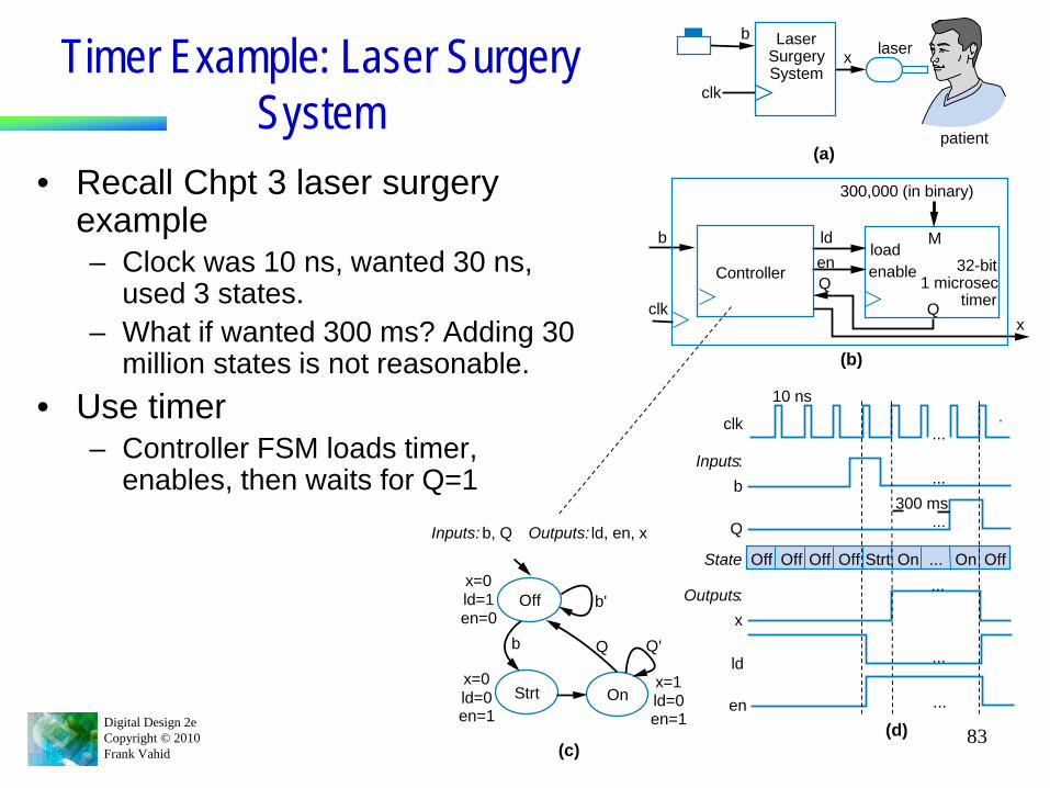
Timer Example: Laser Surgery System
• Recall Chpt 3 laser surgery example– Clock was 10 ns, wanted 30 ns,
used 3 states. – What if wanted 300 ms? Adding 30
million states is not reasonable.• Use timer
– Controller FSM loads timer, enables, then waits for Q=1
(a)
LaserSurgerySystem
xb
clk
laser
patient
(b)
loadenable
Q
32-bit1 microsec
timer
M
Controller
300,000 (in binary)
b
xclk
ldenQ
Inputs: b, Q Outputs: ld, en, x
On
Off
x=1ld=0en=1
x=0ld=1en=0
b'
b Q'Q
Strtx=0ld=0en=1
(c)
Off OffOnOff Off Off ... OnStrt
clk
State
Outputs:
Inputs:
x
b
ld
en
Q
...
...
...
...
...
...
300 ms
10 ns
(d)
Digital Design 2eCopyright © 2010Frank Vahid
84
C
d0
d1
d2
d3e
i0
i0
i1
i2
i3
a0
a1
load
i1
2⋅ 4 8
8
8
8
8Dd
8x y
s1 s0
8-bit4×1
load
load
load
load
reg0
reg1
reg2
reg3
T
A
I
M
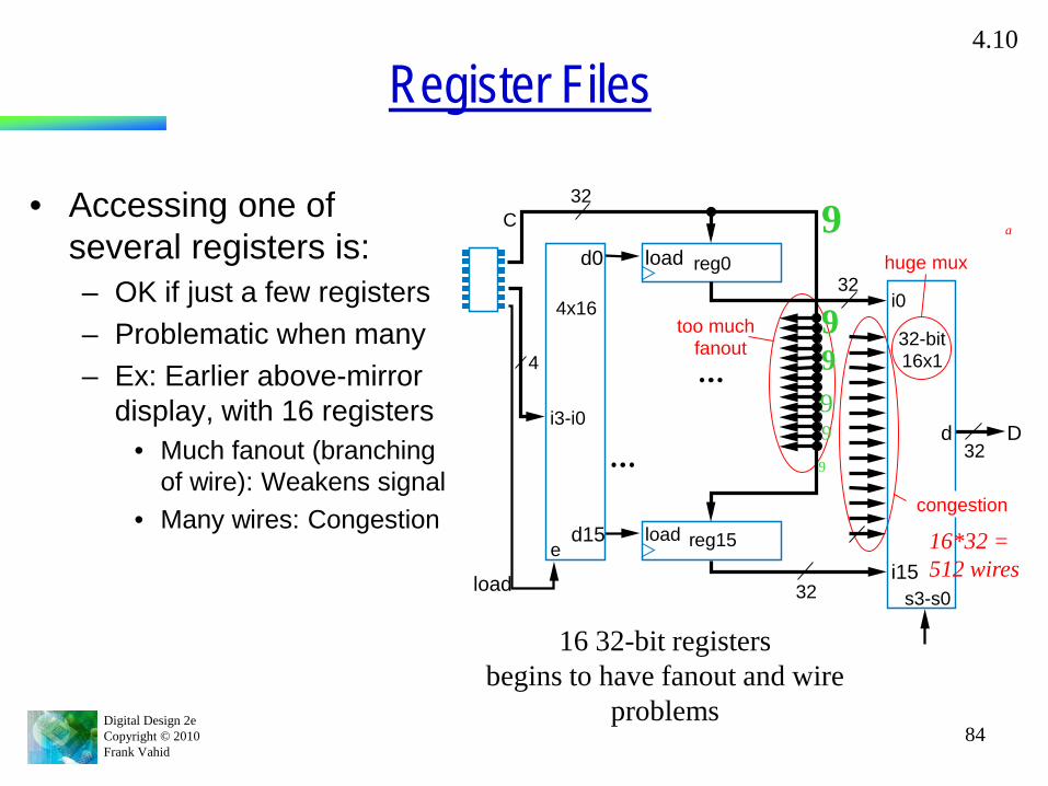
Register Files
• Accessing one of several registers is:– OK if just a few registers– Problematic when many– Ex: Earlier above-mirror
display, with 16 registers• Much fanout (branching
of wire): Weakens signal• Many wires: Congestion
4.10
4 32-bit registers tolerable
congestion
too muchfanout
huge mux
C
d0
d15e
i0
i15load
i3-i0
4x1632
32
32
32
4
Dd
s3-s0
32-bit16x1
load
load
reg0
reg15
a
16 32-bit registers begins to have fanout and wire
problems
9
99999
16*32 = 512 wires
Digital Design 2eCopyright © 2010Frank Vahid
85
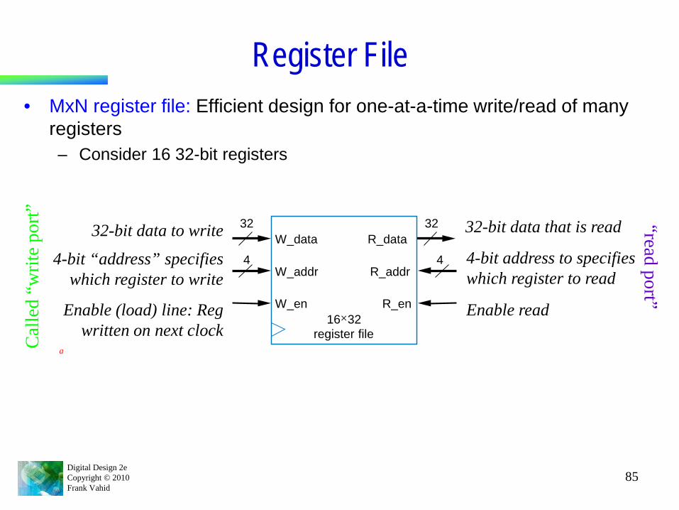
Register File• MxN register file: Efficient design for one-at-a-time write/read of many
registers– Consider 16 32-bit registers
32
4
W_data
W_addr
W_en
32
4
R_data
R_addr
R_en16×32
register filea
32-bit data to write
4-bit “address” specifies which register to write
Enable (load) line: Reg written on next clock
4-bit address to specifies which register to read
Enable read
32-bit data that is read
Cal
led
“writ
e po
rt” “read port”
Digital Design 2eCopyright © 2010Frank Vahid
86
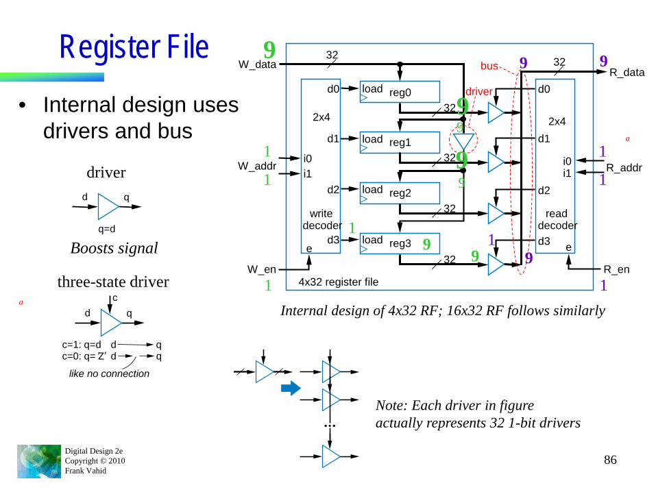
Register File• Internal design uses
drivers and bus a
a
d0
d1
d2
d3e
i0
d0
d1
d2
d3
W_en
W_addr
W_data
i1
2x4
32 32
32
32
32
32
i1i0
e
2x4
load
load
load
load
reg0
reg1
reg2
reg3
R_en
R_addr
R_data
driver
bus
writedecoder
readdecoder
4x32 register file
Internal design of 4x32 RF; 16x32 RF follows similarly
1
1
9
1q
c=1: q=d
c
c=0: q= Z′
d
′ d qd q
like no connection
three-state driver
q
q=d
d
driver
Boosts signal
99
99
9
Note: Each driver in figure actually represents 32 1-bit drivers
1
1
1
1
91
9
9 9
Digital Design 2eCopyright © 2010Frank Vahid
87
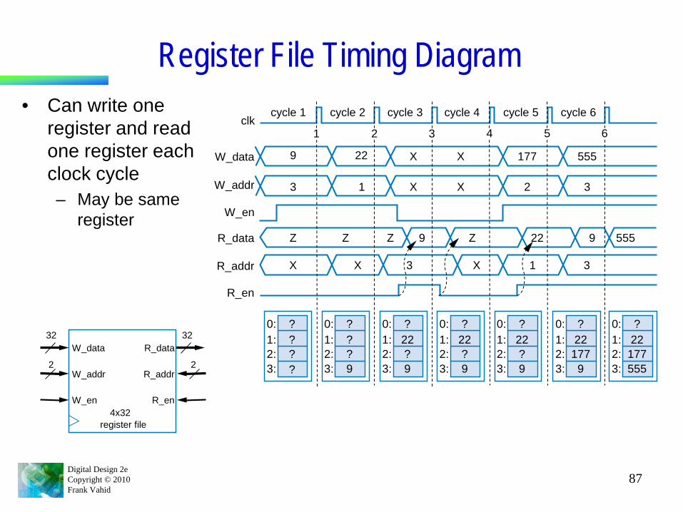
Register File Timing Diagram• Can write one
register and read one register each clock cycle– May be same
register
32
2
32
2
W_data
W_addr
W_en
R_data
R_addr
R_en4x32
register file
0:1:2:3:
???9
0:1:2:3:
?22?9
0:1:2:3:
?22?9
0:1:2:3:
?22?9
0:1:2:3:
?22
1779
0:1:2:3:
?22
177555
0:1:2:3:
????
9
3
Z
X
22
1 X
X
X 2 3
X 177 555
Z Z Z9 9 55522
X X3 31
cycle 1 cycle 2 cycle 3 cycle 4 cycle 5 cycle 6clk
W_data
R_data
W_addr
R_addr
W_en
R_en
1 2 3 654
Digital Design 2eCopyright © 2010Frank Vahid
88
OLD designC
d0
d15e
i0
i15load
i3-i0
4⋅ 1632
32
32
32
4
Dd
s3-s0
32-bit16x1
load
load
reg0
reg15
congestion
too muchfanout
huge mux
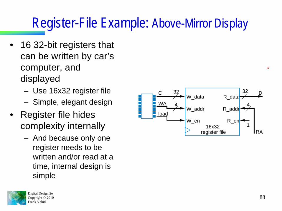
Register-File Example: Above-Mirror Display• 16 32-bit registers that
can be written by car’s computer, and displayed – Use 16x32 register file– Simple, elegant design
• Register file hides complexity internally– And because only one
register needs to be written and/or read at a time, internal design is simple
a
32
4
32
4
1
W_data
W_addr
W_en
R_data
R_addr
R_en16x32
register file
C D
RA
WA
load
Digital Design 2eCopyright © 2010Frank Vahid
89
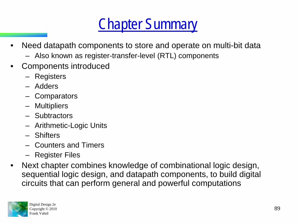
Chapter Summary• Need datapath components to store and operate on multi-bit data
– Also known as register-transfer-level (RTL) components• Components introduced
– Registers– Adders– Comparators – Multipliers – Subtractors– Arithmetic-Logic Units– Shifters– Counters and Timers– Register Files
• Next chapter combines knowledge of combinational logic design, sequential logic design, and datapath components, to build digital circuits that can perform general and powerful computations