Embed Size (px)
Citation preview

Digital Design, Kyung Hee Univ.
1
Chapter 4. Combinational Logic
Tong In Oh

Digital Design, Kyung Hee Univ.
2
4.1 Introduction• Combinational logic:
• Logic gates• Output determined from only the present combination of inputs• Specified by a set of Boolean functions
• Sequential logic:• Employ storage elements in addition to logic gates• Output determined by present inputs and the state of the storage elements• Specified by a time sequence of inputs and internal states
Digital Design, Kyung Hee Univ.
3
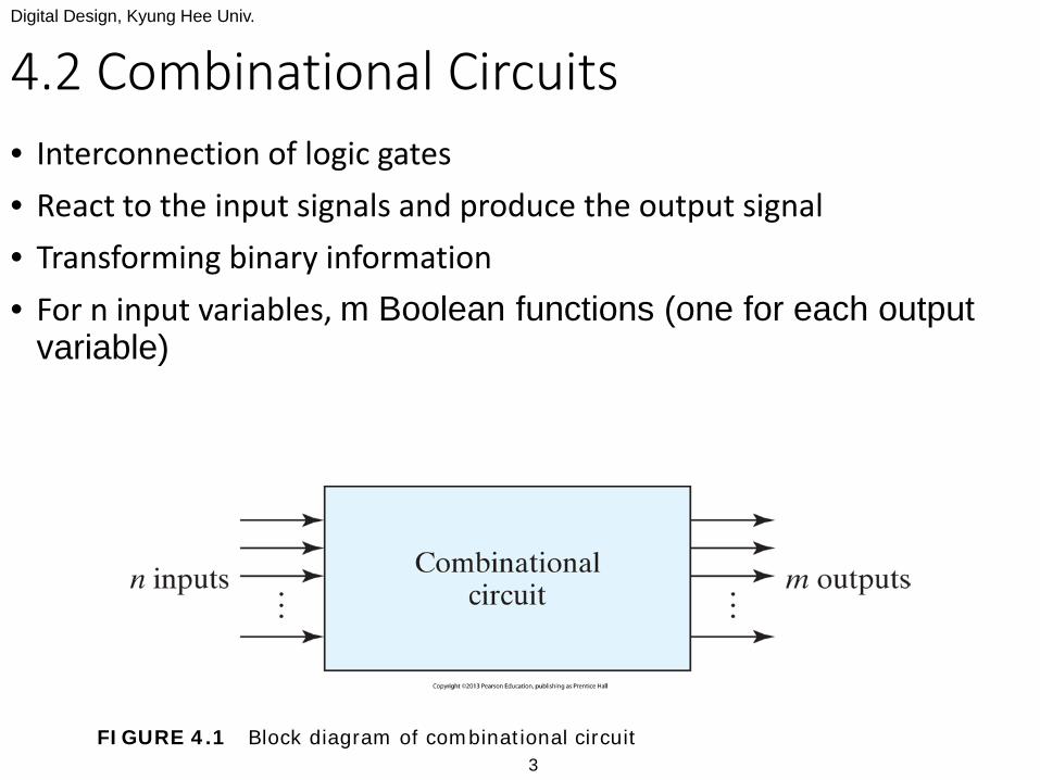
4.2 Combinational Circuits• Interconnection of logic gates• React to the input signals and produce the output signal• Transforming binary information• For n input variables, m Boolean functions (one for each output
variable)
FIGURE 4.1 Block diagram of combinational circuit

Digital Design, Kyung Hee Univ.
4
Goals• To formulate systematic analysis• Design procedures for combinational circuits• Provide a useful catalog of elementary functions
• Two tasks• Analyze the behavior of a given logic circuit• Synthesize a circuit for a given behavior
• The most important standard combinational circuits• Adders, subtractors, comparators, decoders, encoders, and multiplexers
Digital Design, Kyung Hee Univ.
5
4.3 Analysis Procedure• Determine the function implemented in the circuit• Boolean functions, a truth table, explanation of the circuit operation
from the given logic diagram1. Combinational and not sequential ?
• No feedback paths or memory elements
2. To obtain the output Boolean functions1. Label all gate outputs that are a function of input variables with arbitrary
symbols but with meaningful names. Determine the Boolean functions for each gate output.
2. Label the gates that are a function of input variables and previously labeled gates with other arbitrary symbols. Find the Boolean functions for these gates.
3. Repeat the process outlined in step 2 until the outputs of the circuit are obtained.
4. By repeated substitution of previously defined functions, obtain the output Boolean functions in terms of input variables.

Digital Design, Kyung Hee Univ.
6
• Determine the function from a given logic diagram to a set of Boolean functions or a truth table
FIGURE 4.2 Logic diagram for analysis example

Digital Design, Kyung Hee Univ.
7
Truth Table• To obtain truth table
1. Determine the number of input variables in the circuit. List the binary numbers from 0 to (2n - 1) in a table.
2. Label the outputs of selected gates with arbitrary symbols.3. Obtain the truth table for the outputs of those gates which are a function of
the input variables only.4. Proceed to obtain the truth table for the outputs of those gates which are a
function of previously defined values until the columns for all outputs are determined
Identical to the truth table of the full adder

Digital Design, Kyung Hee Univ.
8
4.4 Design Procedure• Start from the specification of the design objective• Culminate in a logic circuit diagram or a set of Boolean functions
1. From the specifications of the circuit, determine the required number of inputs and outputs and assign a symbol to each.
2. Derive the truth table that defines the required relationship between inputs and outputs.
3. Obtain the simplified Boolean functions for each output as a function of the input variables.
4. Draw the logic diagram and verify the correctness of the design (manually or by simulation).
• Interpret verbal specifications correctly in the truth table• Constraints
• Number of gates, number of inputs to a gate, propagation time of the signal through the gates, number of interconnections, limitations of the driving capability of each gate, various other criteria
Digital Design, Kyung Hee Univ.
9
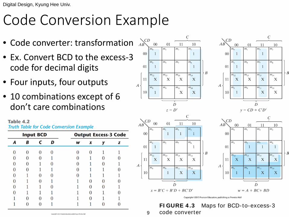
Code Conversion Example• Code converter: transformation• Ex. Convert BCD to the excess-3
code for decimal digits• Four inputs, four outputs• 10 combinations except of 6
don’t care combinations
FIGURE 4.3 Maps for BCD-to-excess-3 code converter

Digital Design, Kyung Hee Univ.
10FIGURE 4.4 Logic diagram for BCD-to-excess-3 code converter
Digital Design, Kyung Hee Univ.
11
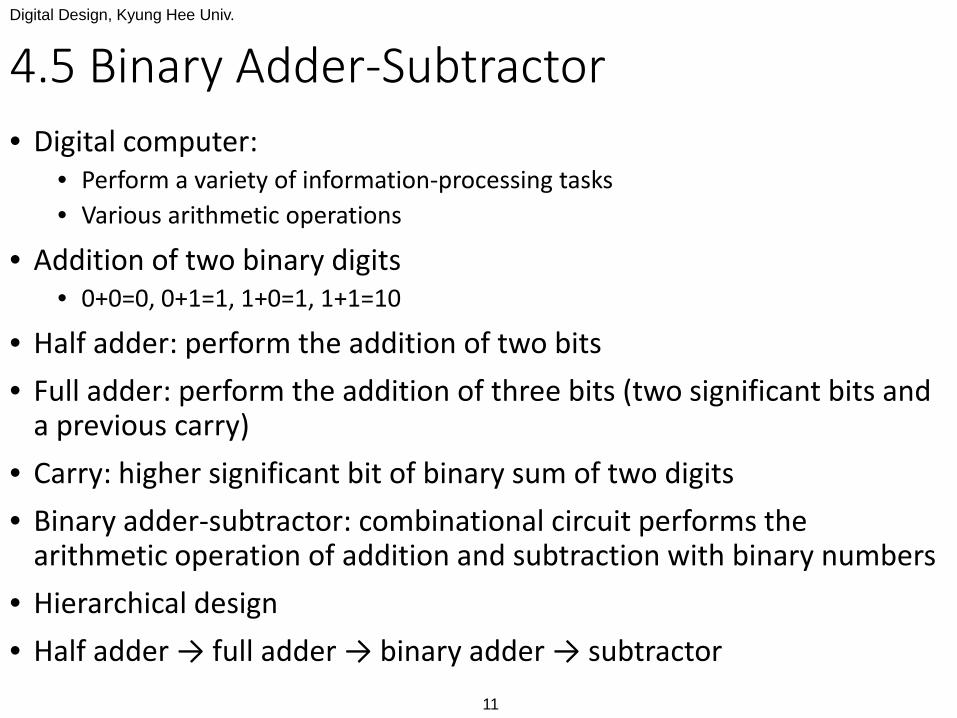
4.5 Binary Adder-Subtractor• Digital computer:
• Perform a variety of information-processing tasks• Various arithmetic operations
• Addition of two binary digits• 0+0=0, 0+1=1, 1+0=1, 1+1=10
• Half adder: perform the addition of two bits• Full adder: perform the addition of three bits (two significant bits and
a previous carry)• Carry: higher significant bit of binary sum of two digits• Binary adder-subtractor: combinational circuit performs the
arithmetic operation of addition and subtraction with binary numbers• Hierarchical design• Half adder → full adder → binary adder → subtractor
Digital Design, Kyung Hee Univ.
12
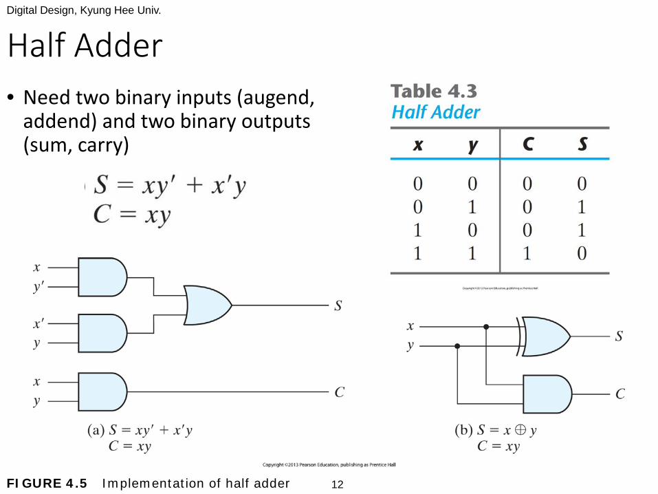
Half Adder• Need two binary inputs (augend,
addend) and two binary outputs (sum, carry)
FIGURE 4.5 Implementation of half adder
Digital Design, Kyung Hee Univ.
13
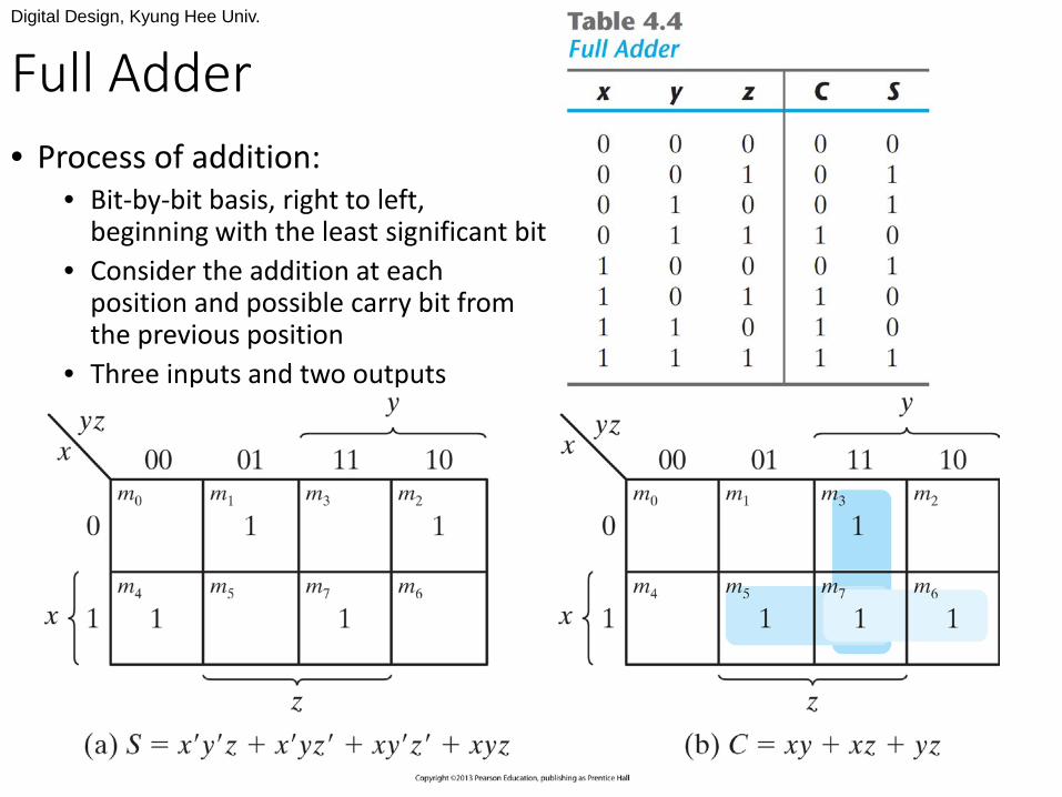
Full Adder• Process of addition:
• Bit-by-bit basis, right to left, beginning with the least significant bit
• Consider the addition at each position and possible carry bit from the previous position
• Three inputs and two outputs

Digital Design, Kyung Hee Univ.
14
FIGURE 4.7Implementation of full adder in sum-of-products form
FIGURE 4.8 Implementation of full adder with two half adders and an OR gate
Digital Design, Kyung Hee Univ.
15
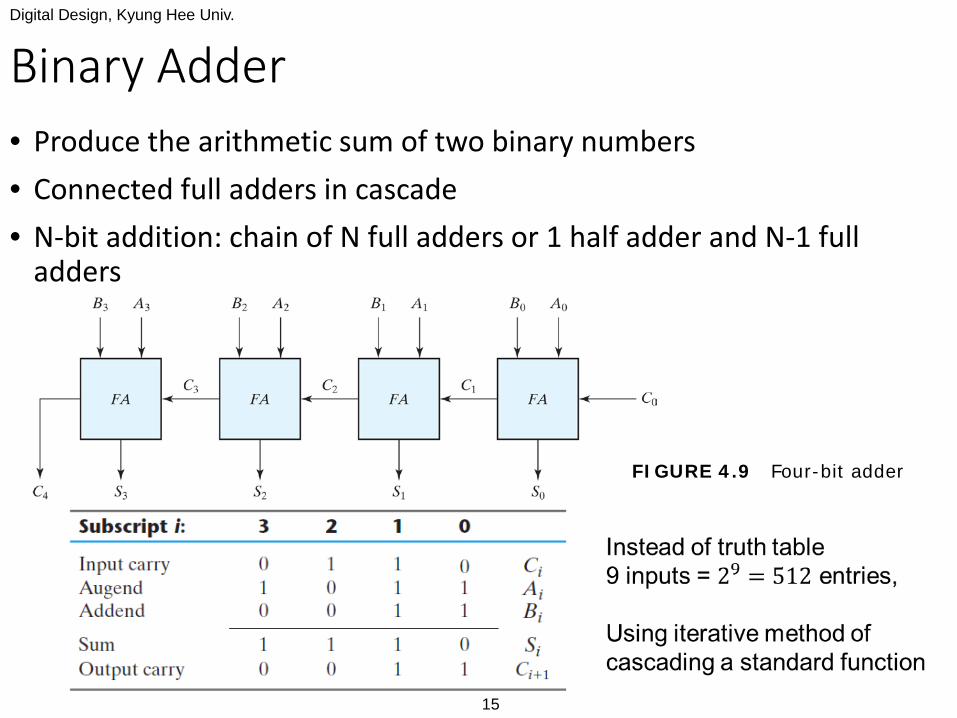
Binary Adder• Produce the arithmetic sum of two binary numbers• Connected full adders in cascade• N-bit addition: chain of N full adders or 1 half adder and N-1 full
adders
FIGURE 4.9 Four-bit adder
Digital Design, Kyung Hee Univ.
16
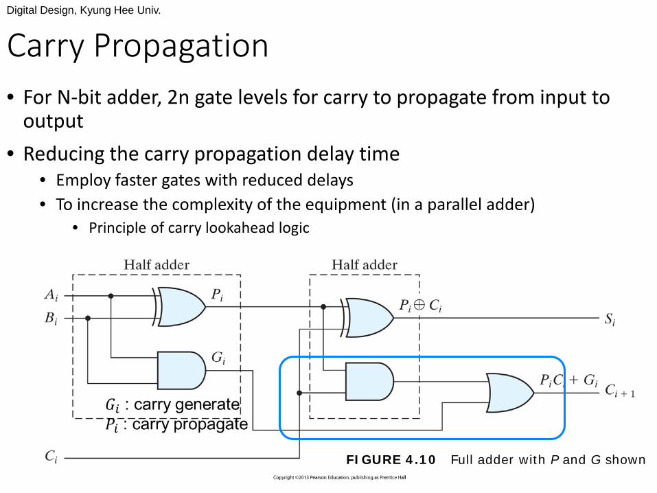
Carry Propagation• For N-bit adder, 2n gate levels for carry to propagate from input to
output• Reducing the carry propagation delay time
• Employ faster gates with reduced delays• To increase the complexity of the equipment (in a parallel adder)
• Principle of carry lookahead logic
FIGURE 4.10 Full adder with P and G shown
Digital Design, Kyung Hee Univ.
17
+
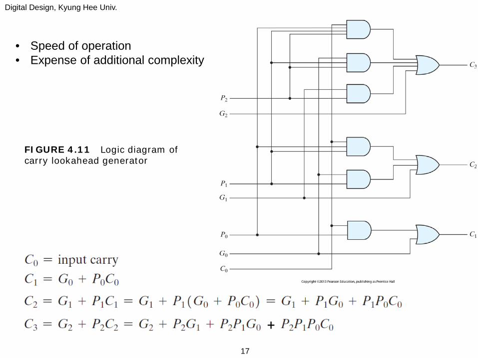
• Speed of operation• Expense of additional complexity
FIGURE 4.11 Logic diagram of carry lookahead generator

Digital Design, Kyung Hee Univ.
18
FIGURE 4.12 Four-bit adder with carry lookahead

Digital Design, Kyung Hee Univ.
19
Binary Subtractor• A-B:
• Adding A to 2’s complement of B• 2’s complement: inverters and sum through the input carry
FIGURE 4.13 Four-bit adder–subtractor (with overflow detection)
Digital Design, Kyung Hee Univ.
20
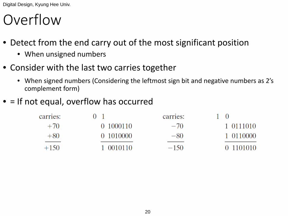
Overflow• Detect from the end carry out of the most significant position
• When unsigned numbers
• Consider with the last two carries together• When signed numbers (Considering the leftmost sign bit and negative numbers as 2’s
complement form)
• = If not equal, overflow has occurred
Digital Design, Kyung Hee Univ.
21
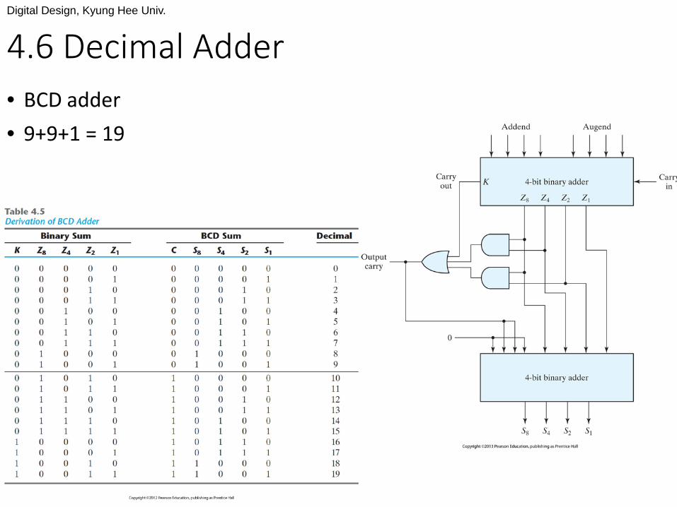
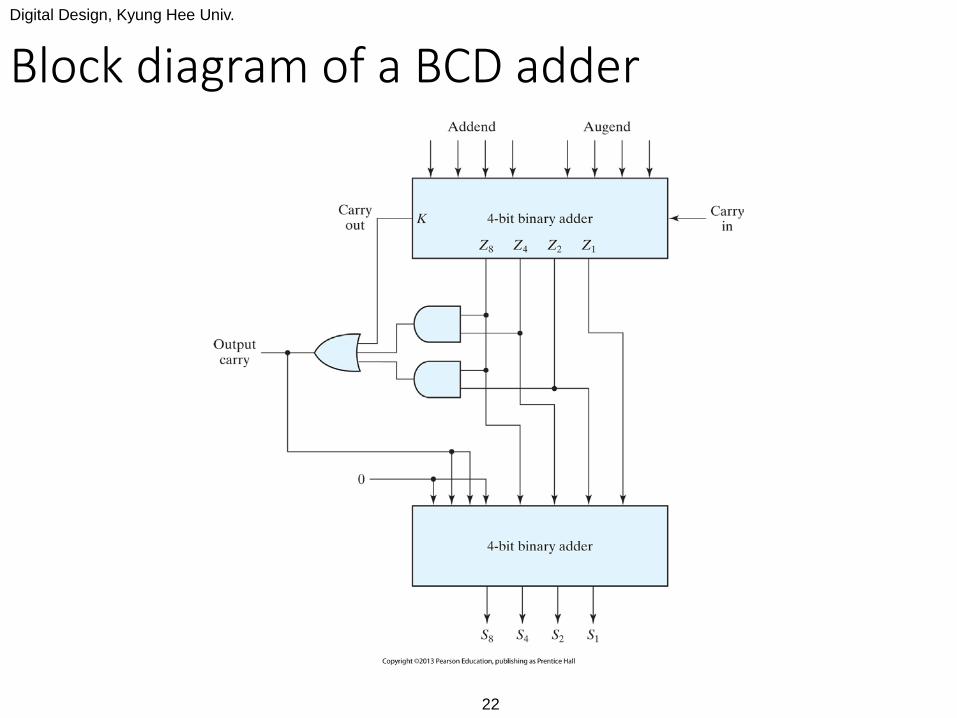
4.6 Decimal Adder• BCD adder• 9+9+1 = 19
Digital Design, Kyung Hee Univ.
22
Block diagram of a BCD adder

Digital Design, Kyung Hee Univ.
23
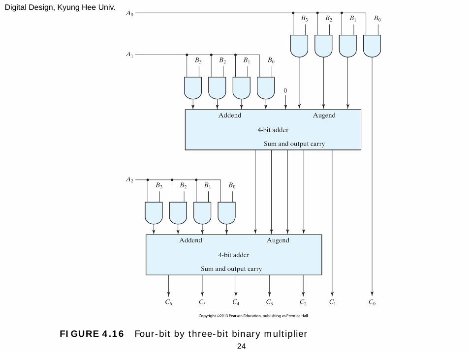
4.7 Binary Multiplier
FIGURE 4.15 Two-bit by two-bit binary multiplier
J multiplier bitsK multiplicand bits(JXK) AND gates(J-1) K-bit addersResult: product of (J+K) bits
Digital Design, Kyung Hee Univ.
24FIGURE 4.16 Four-bit by three-bit binary multiplier
Digital Design, Kyung Hee Univ.
25
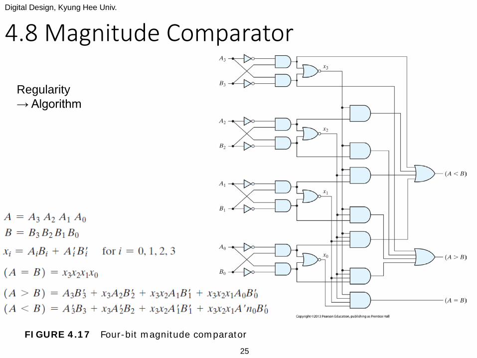
4.8 Magnitude Comparator
FIGURE 4.17 Four-bit magnitude comparator
Regularity→ Algorithm

Digital Design, Kyung Hee Univ.
26
4.9 Decoders
FIGURE 4.18 Three-to-eight-line decoder
• Convert binary information from n input lines to a maximum of 2n unique output lines
• 2n (or fewer) minterms of n input variables
• Generate a unique output• N-to-M line decoder• Code converter

Digital Design, Kyung Hee Univ.
27
Decoder-Demultiplexer
FIGURE 4.19 Two-to-four-line decoder with enable input
0
A decoder with enable input can function as a demultiplexerEx) one to four line demultiplexer (E: data input line, A and B: selection inputs)
Digital Design, Kyung Hee Univ.
28
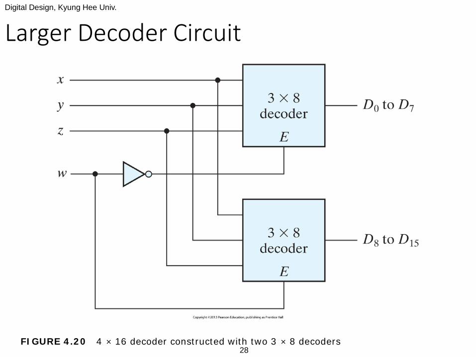
Larger Decoder Circuit
FIGURE 4.20 4 × 16 decoder constructed with two 3 × 8 decoders
Digital Design, Kyung Hee Univ.
29
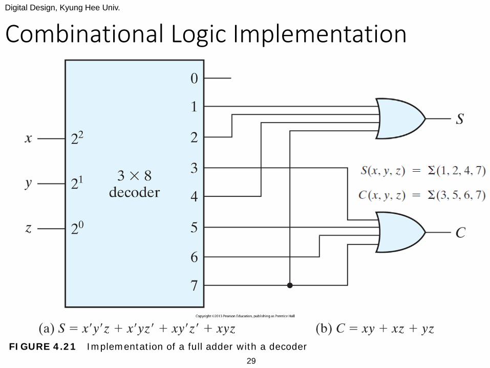
Combinational Logic Implementation
FIGURE 4.21 Implementation of a full adder with a decoder
Digital Design, Kyung Hee Univ.
30
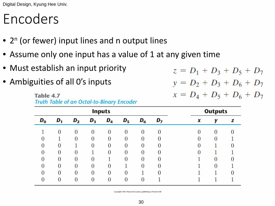
Encoders• 2n (or fewer) input lines and n output lines• Assume only one input has a value of 1 at any given time• Must establish an input priority• Ambiguities of all 0’s inputs
Digital Design, Kyung Hee Univ.
31
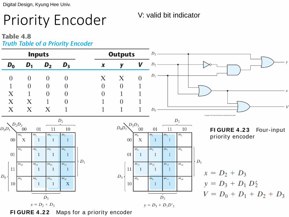
Priority Encoder V: valid bit indicator
FIGURE 4.22 Maps for a priority encoder
FIGURE 4.23 Four-input priority encoder
Digital Design, Kyung Hee Univ.
32
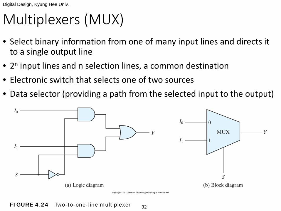
Multiplexers (MUX)• Select binary information from one of many input lines and directs it
to a single output line• 2n input lines and n selection lines, a common destination• Electronic switch that selects one of two sources• Data selector (providing a path from the selected input to the output)
FIGURE 4.24 Two-to-one-line multiplexer
Digital Design, Kyung Hee Univ.
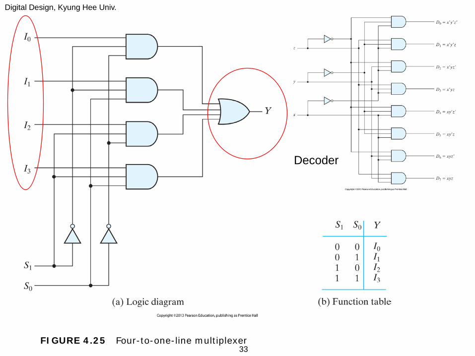
33FIGURE 4.25 Four-to-one-line multiplexer
Decoder

Digital Design, Kyung Hee Univ.
34
Multiple-bit Selection Logic
FIGURE 4.26 Quadruple two-to-one-line multiplexer
Digital Design, Kyung Hee Univ.
35
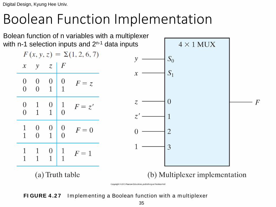
Boolean Function Implementation
FIGURE 4.27 Implementing a Boolean function with a multiplexer
Bolean function of n variables with a multiplexer with n-1 selection inputs and 2n-1 data inputs

Digital Design, Kyung Hee Univ.
36FIGURE 4.28 Implementing a four-input function with a multiplexer
Digital Design, Kyung Hee Univ.
37
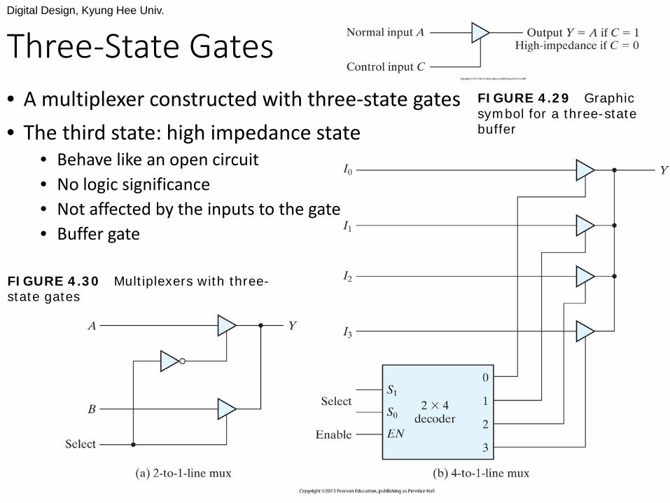
• A multiplexer constructed with three-state gates• The third state: high impedance state
• Behave like an open circuit• No logic significance• Not affected by the inputs to the gate• Buffer gate
Three-State GatesFIGURE 4.29 Graphic symbol for a three-state buffer
FIGURE 4.30 Multiplexers with three-state gates