Embed Size (px)
Citation preview
8/8/2019 Chapter 3 Part2 Vhdl and Vlsi
http://slidepdf.com/reader/full/chapter-3-part2-vhdl-and-vlsi 1/13
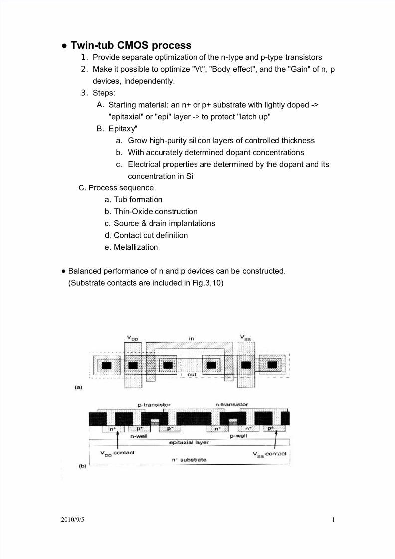
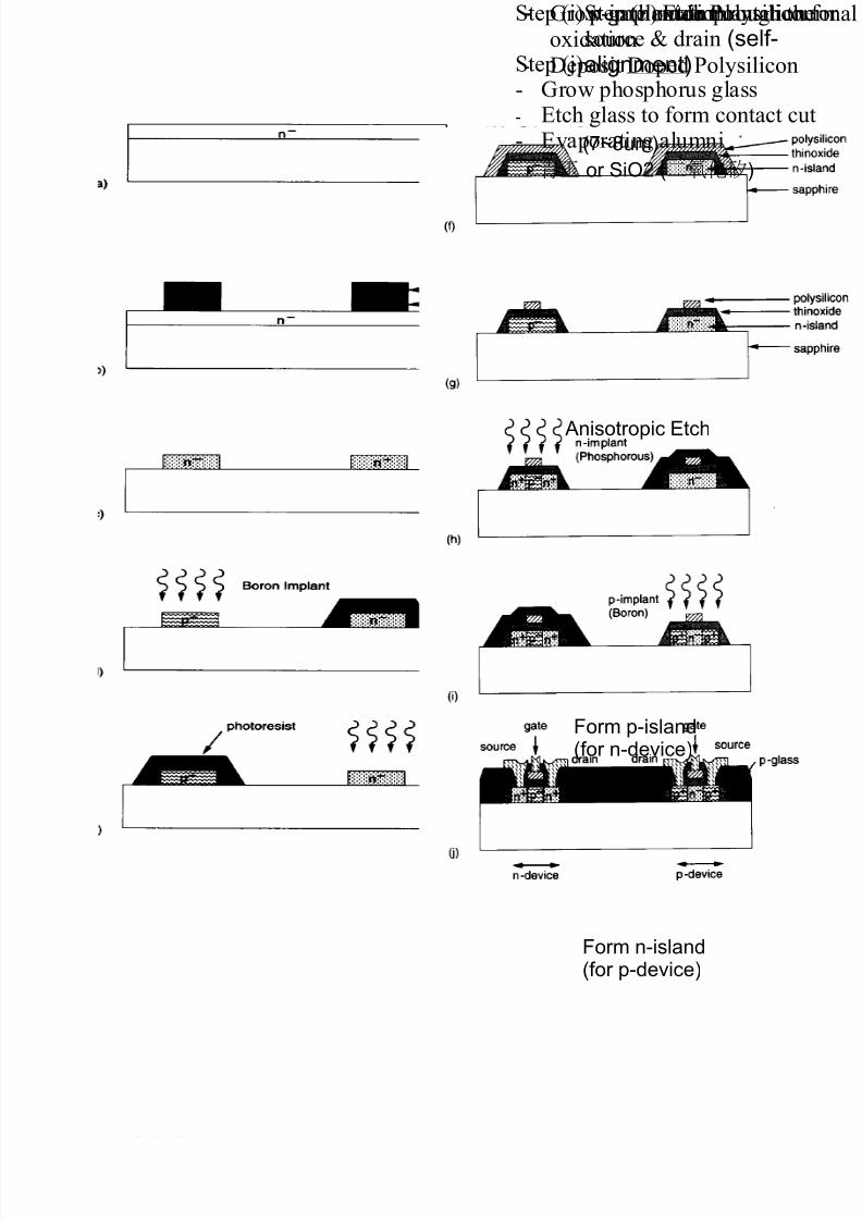
● Twin-tub CMOS process1. Provide separate optimization of the n-type and p-type transistors
2. Make it possible to optimize "Vt", "Body effect", and the "Gain" of n, p
devices, independently.
3. Steps:
A. Starting material: an n+ or p+ substrate with lightly doped ->
"epitaxial" or "epi" layer -> to protect "latch up"
B. Epitaxy"
a. Grow high-purity silicon layers of controlled thickness
b. With accurately determined dopant concentrations
c. Electrical properties are determined by the dopant and its
concentration in Si
C. Process sequence
a. Tub formation
b. Thin-Oxide construction
c. Source & drain implantations
d.Contact cut definition
e. Metallization
● Balanced performance of n and p devices can be constructed.
(Substrate contacts are included in Fig.3.10)
2010/9/5 1
8/8/2019 Chapter 3 Part2 Vhdl and Vlsi
http://slidepdf.com/reader/full/chapter-3-part2-vhdl-and-vlsi 2/13
2010/9/5 2
- Grow gate oxide through thermaloxidation
- Deposit Doped Polysilicon
Etch PolysiliconStep (h): n-implantation for source & drain (self-alignment)
Step (i) p-implantation
Step (j)- Grow phosphorus glass- Etch glass to form contact cut- Evaporating alumni(7~8um)
青玉 or SiO2 (二氧化矽)
Anisotropic Etch
Form p-island(for n-device)
Form n-island(for p-device)
8/8/2019 Chapter 3 Part2 Vhdl and Vlsi
http://slidepdf.com/reader/full/chapter-3-part2-vhdl-and-vlsi 3/13
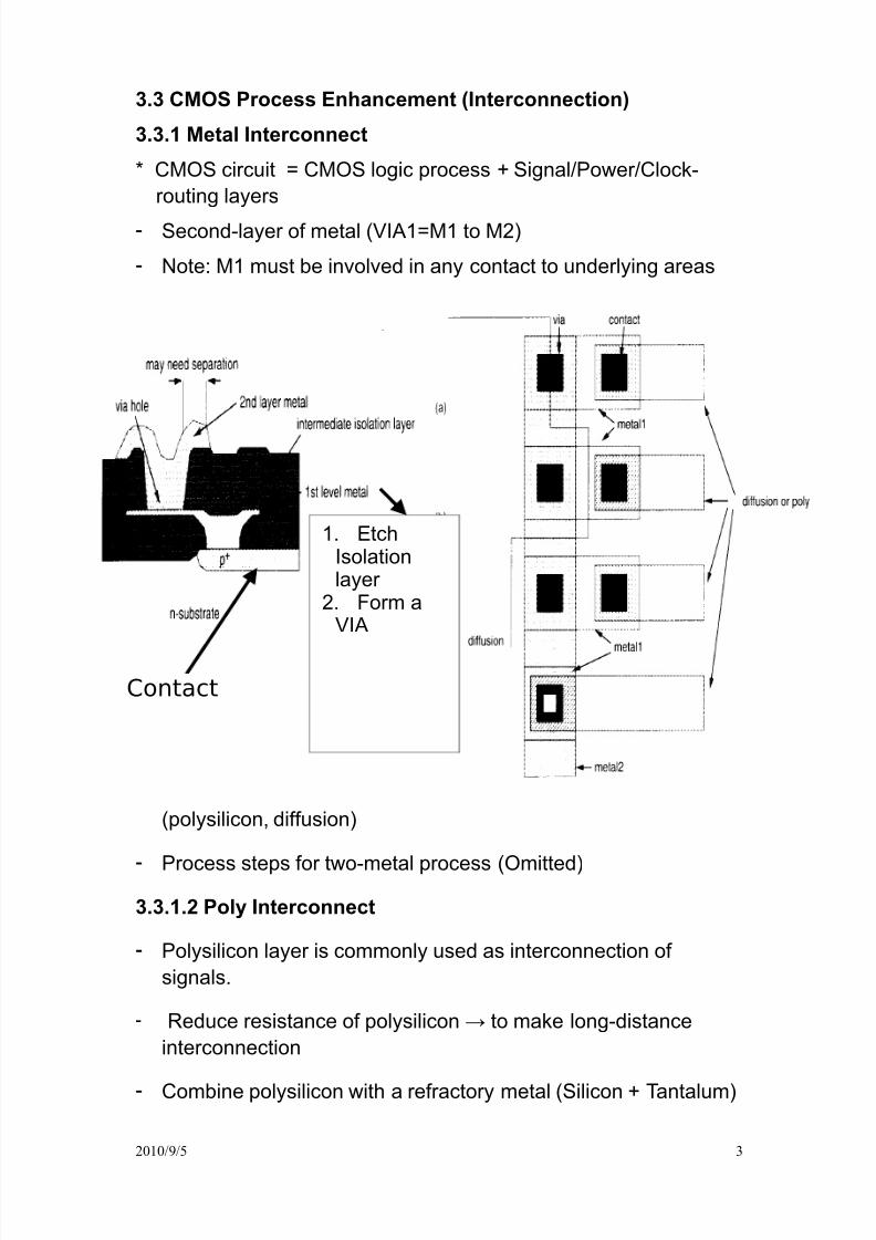
3.3 CMOS Process Enhancement (Interconnection)
3.3.1 Metal Interconnect
* CMOS circuit = CMOS logic process + Signal/Power/Clock-
routing layers
- Second-layer of metal (VIA1=M1 to M2)
- Note: M1 must be involved in any contact to underlying areas
(polysilicon, diffusion)
-
Process steps for two-metal process (Omitted)
3.3.1.2 Poly Interconnect
- Polysilicon layer is commonly used as interconnection of
signals.
- Reduce resistance of polysilicon → to make long-distance
interconnection
-Combine polysilicon with a refractory metal (Silicon + Tantalum)
2010/9/5 3
1. EtchIsolationlayer
2. Form aVIA
Contact
8/8/2019 Chapter 3 Part2 Vhdl and Vlsi
http://slidepdf.com/reader/full/chapter-3-part2-vhdl-and-vlsi 4/13
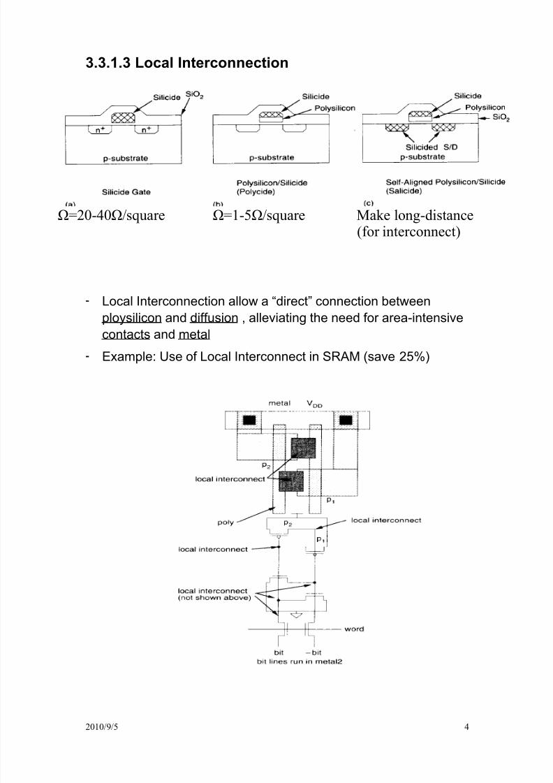
3.3.1.3 Local Interconnection
- Local Interconnection allow a “direct” connection between
ploysilicon and diffusion , alleviating the need for area-intensive
contacts and metal
- Example: Use of Local Interconnect in SRAM (save 25%)
2010/9/5 4
Ω=20-40Ω/square Ω=1-5Ω/square Make long-distance(for interconnect)
8/8/2019 Chapter 3 Part2 Vhdl and Vlsi
http://slidepdf.com/reader/full/chapter-3-part2-vhdl-and-vlsi 5/13
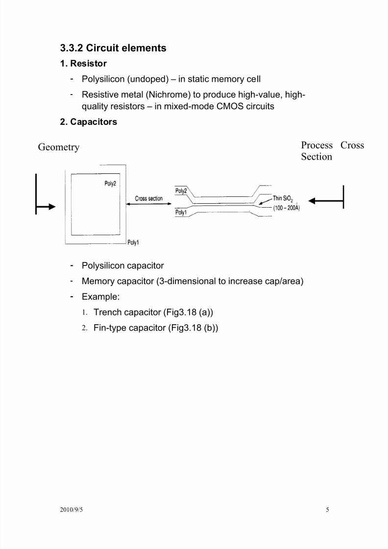
3.3.2 Circuit elements
1. Resistor
- Polysilicon (undoped) – in static memory cell
- Resistive metal (Nichrome) to produce high-value, high-quality resistors – in mixed-mode CMOS circuits
2. Capacitors
- Polysilicon capacitor
- Memory capacitor (3-dimensional to increase cap/area)
- Example:
1. Trench capacitor (Fig3.18 (a))
2. Fin-type capacitor (Fig3.18 (b))
2010/9/5 5
Process CrossSection
Geometry
8/8/2019 Chapter 3 Part2 Vhdl and Vlsi
http://slidepdf.com/reader/full/chapter-3-part2-vhdl-and-vlsi 6/13
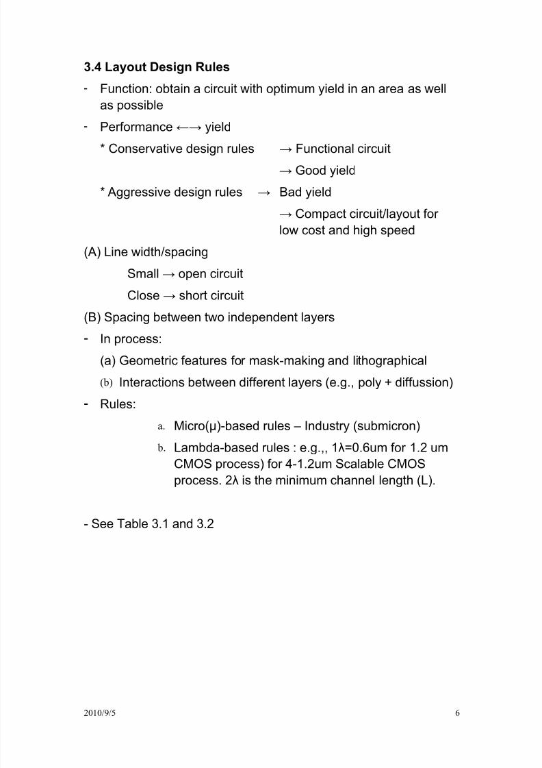
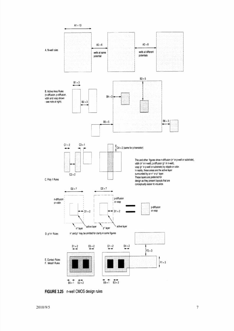
3.4 Layout Design Rules
- Function: obtain a circuit with optimum yield in an area as well
as possible
- Performance ←→ yield
* Conservative design rules → Functional circuit
→ Good yield
* Aggressive design rules → Bad yield
→ Compact circuit/layout for
low cost and high speed
(A) Line width/spacing
Small → open circuit
Close → short circuit
(B) Spacing between two independent layers
- In process:
(a) Geometric features for mask-making and lithographical
(b) Interactions between different layers (e.g., poly + diffussion)
-Rules:
a. Micro(μ)-based rules – Industry (submicron)
b. Lambda-based rules : e.g.,, 1λ=0.6um for 1.2 um
CMOS process) for 4-1.2um Scalable CMOS
process. 2λ is the minimum channel length (L).
- See Table 3.1 and 3.2
2010/9/5 6
8/8/2019 Chapter 3 Part2 Vhdl and Vlsi
http://slidepdf.com/reader/full/chapter-3-part2-vhdl-and-vlsi 7/13
2010/9/5 7
8/8/2019 Chapter 3 Part2 Vhdl and Vlsi
http://slidepdf.com/reader/full/chapter-3-part2-vhdl-and-vlsi 8/13
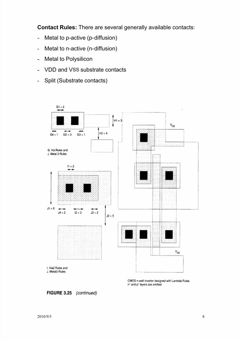
Contact Rules: There are several generally available contacts:
- Metal to p-active (p-diffusion)
- Metal to n-active (n-diffusion)
- Metal to Polysilicon
- VDD and VSS substrate contacts
- Split (Substrate contacts)
2010/9/5 8
8/8/2019 Chapter 3 Part2 Vhdl and Vlsi
http://slidepdf.com/reader/full/chapter-3-part2-vhdl-and-vlsi 9/13
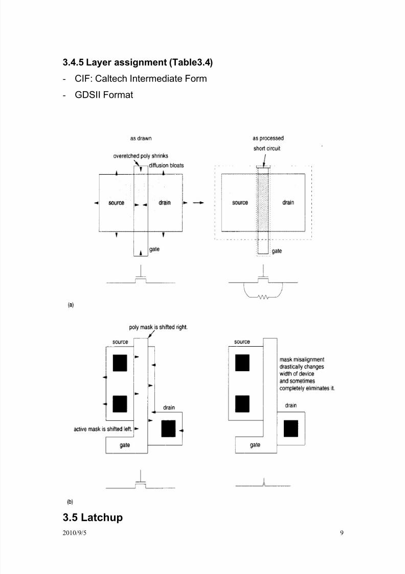
3.4.5 Layer assignment (Table3.4)
- CIF: Caltech Intermediate Form
- GDSII Format
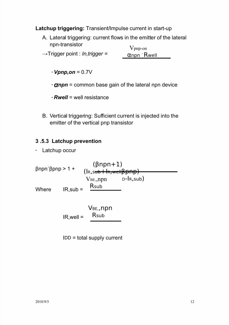
3.5 Latchup
2010/9/5 9
8/8/2019 Chapter 3 Part2 Vhdl and Vlsi
http://slidepdf.com/reader/full/chapter-3-part2-vhdl-and-vlsi 10/13
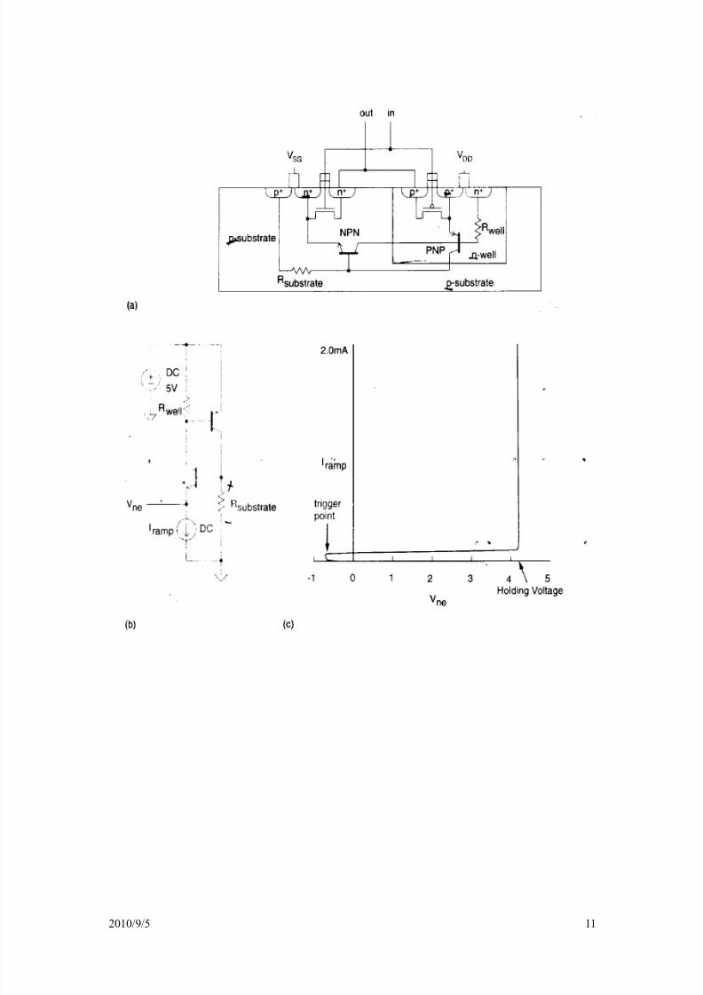
- Latchup : Shorting of VDD and Vss lines → Chip breakdown
- Latchup Equivalent Circuit:
Vertical : pnp
- p = source/drain of p device (Emitter)
-n = n-well (Base)
- p = p-substrate (Collector)
Lateral : npn
- n = source/drain of n device (Emitter)
- p= p-substrate (Base)
- n= n-well (Collector)
Rsubstrate, Rwell
- Parasitic devices and resistors
2010/9/5 10
8/8/2019 Chapter 3 Part2 Vhdl and Vlsi
http://slidepdf.com/reader/full/chapter-3-part2-vhdl-and-vlsi 11/13
2010/9/5 11
8/8/2019 Chapter 3 Part2 Vhdl and Vlsi
http://slidepdf.com/reader/full/chapter-3-part2-vhdl-and-vlsi 12/13
8/8/2019 Chapter 3 Part2 Vhdl and Vlsi
http://slidepdf.com/reader/full/chapter-3-part2-vhdl-and-vlsi 13/13
Observation to prevent latchup:
1. Reduce the resistor values
2. Reduce the gain of the parasitic devices
- Approach:
1.Latchup-resistant CMOS process
2. Layout techniques (see section 3.5.4,3.5.5)
3.6 Technology-related CAD tools
-
Design Rule Check (DRC): On-line and Off-line (Dracula)(3.6.1)
- Circuit extraction (Layout Parameter Extraction, LPE) (3.6.2)
- CMOS process simulator (Process Input Description Language
(PIDL))(sec.3.9) and Supreme by Stanford University.
2010/9/5 13