Embed Size (px)
Citation preview

CHAPTER 3
METHODOLOGY
3.1 Hardware Requirement
The hardware part will be explained first as this project comprise of several
important hardware and the fact that the hardware part are designed and built first before
anything else. Below show the hardware that was used to build this project:
• Microcontroller
• MAX 232
• Receiver/Transceiver (RX/TX)
• Analog/Digital Converter (ADC)
• Camera subsystem
3.1.1 Microcontroller
The board is built around Atmel AT89S52 microcontroller. As the
microcontroller is the core of this project, the project was started by choosing the suitable
microcontroller for it. At first, it was decided that Atmel AT89S51 to be used due to it
lower cost but after consideration of the processing power and the memory that this
project needed, the AT89S52 was chosen as it has 8K Bytes of In-System Programmable
(ISP) Flash Memory in comparable to AT89S51 which only has 4K Bytes of In-System
Programmable (ISP) Flash Memory.
19

The AT89S52 is a low-power, high-performance CMOS 8-bit microcontroller
with 8K bytes of in-system programmable Flash memory. The device is compatible with
the industry- standard 80C51 instruction set and pin out. The on-chip Flash allows the
program memory to be reprogrammed in-system or by a conventional nonvolatile
memory programmer.
By combining a versatile 8-bit CPU with in-system programmable Flash on a
monolithic chip, it provides a highly-flexible and cost-effective solution to this project.
Figure 3.1: AT89S52 Microcontroller
20
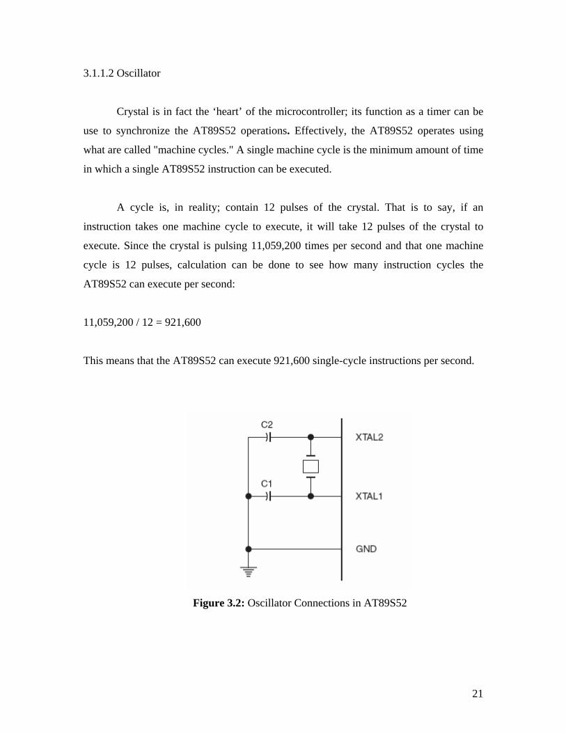
3.1.1.2 Oscillator
Crystal is in fact the ‘heart’ of the microcontroller; its function as a timer can be
use to synchronize the AT89S52 operations. Effectively, the AT89S52 operates using
what are called "machine cycles." A single machine cycle is the minimum amount of time
in which a single AT89S52 instruction can be executed.
A cycle is, in reality; contain 12 pulses of the crystal. That is to say, if an
instruction takes one machine cycle to execute, it will take 12 pulses of the crystal to
execute. Since the crystal is pulsing 11,059,200 times per second and that one machine
cycle is 12 pulses, calculation can be done to see how many instruction cycles the
AT89S52 can execute per second:
11,059,200 / 12 = 921,600
This means that the AT89S52 can execute 921,600 single-cycle instructions per second.
Figure 3.2: Oscillator Connections in AT89S52
21
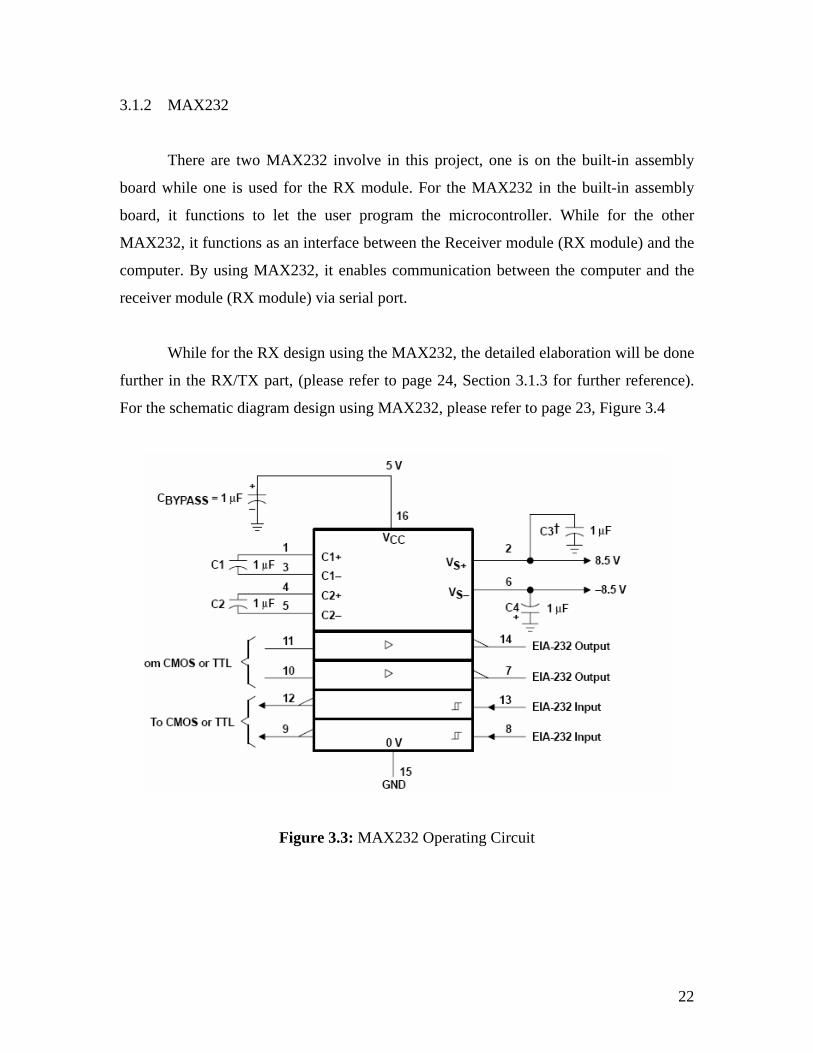
3.1.2 MAX232
There are two MAX232 involve in this project, one is on the built-in assembly
board while one is used for the RX module. For the MAX232 in the built-in assembly
board, it functions to let the user program the microcontroller. While for the other
MAX232, it functions as an interface between the Receiver module (RX module) and the
computer. By using MAX232, it enables communication between the computer and the
receiver module (RX module) via serial port.
While for the RX design using the MAX232, the detailed elaboration will be done
further in the RX/TX part, (please refer to page 24, Section 3.1.3 for further reference).
For the schematic diagram design using MAX232, please refer to page 23, Figure 3.4
Figure 3.3: MAX232 Operating Circuit
22
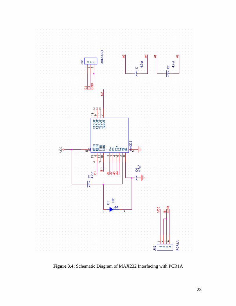
Figure 3.4: Schematic Diagram of MAX232 Interfacing with PCR1A
23

3.1.3 Receiver and Transceiver Module (RX/TX Module)
The RX module used in this project is the PCR1A model. It used DC voltage of
5V and the receiving frequency range of 315 MHz to 433 MHz, while its receiver
sensitivity is 105DBm. For this project, the PCR1A are connected to MAX232, the
connection is done to enable connection to the PC based station via serial port. For the
schematic of the diagram, please refer back to Figure 3.4
Incoming data
PC based station
MAX 232 RX model
Figure 3.5: RX/TX Block Diagram
Figure 3.6: Receiver Model (RX)
For the TX module, it was decided to use the F05P model. It has transmitting
frequency 315 MHz or 433 MHz. It can transmit up to 24 meter in length for 315 MHz
while the frequency of 433 MHz can transmit up to 18 meter. Figure 3.7 on the next page
show the F05P model
24

Figure 3.7: Transceiver Model (TX)
Testing was done to both the TX and RX for the RF signal quality and both of
them proof to be able to transmit signal and receive the signal in satisfactory result.
Figure 3.8 below, and the Figure 3.9 and 3.10 on the next page shows the results from the
testing. Testing was done using random data from the microcontroller to be sent from the
TX to the RX in 10 meter range.
Figure 3.8: Comparisons between Modulated and Demodulated Data
25
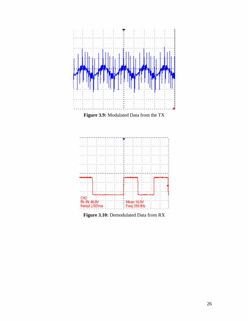
Figure 3.9: Modulated Data from the TX
Figure 3.10: Demodulated Data from RX
26

3.1.4 Analog/Digital Converter (ADC)
The 8-bit µP compatible A/D converter that was used here is the ADC0804.
ADC0804 are CMOS 8-bit successive approximation A/D converters that use a
differential potentiometer ladder. The ADC is used to enable the connection between the
microcontroller and the camera. Since the camera output is analog, the ADC is needed to
convert the data back to digital in order to enable the microcontroller to communicate
with the camera. The clock for the A/D can be derived from the CPU clock or an external
RC can be added to provide self-clocking. The formula used to count the clock frequency
is fclk= RC1.11
, for capacitor value, 151 pF was used while for the resistor value, 10K
Ohms, was used. The calculated value are, fclk= )151)(ohms10(1.11
pFk, = 602046 Hz,
More elaborate explanation can be seen from Section 3.1.6. For the schematic diagram,
please refer to page 28, Figure 3.12.
Figure 3.11: Analog/Digital Converter (ADC0804 type)
27

Figure 3.12: Schematic Diagram Design Using ADC0804
28
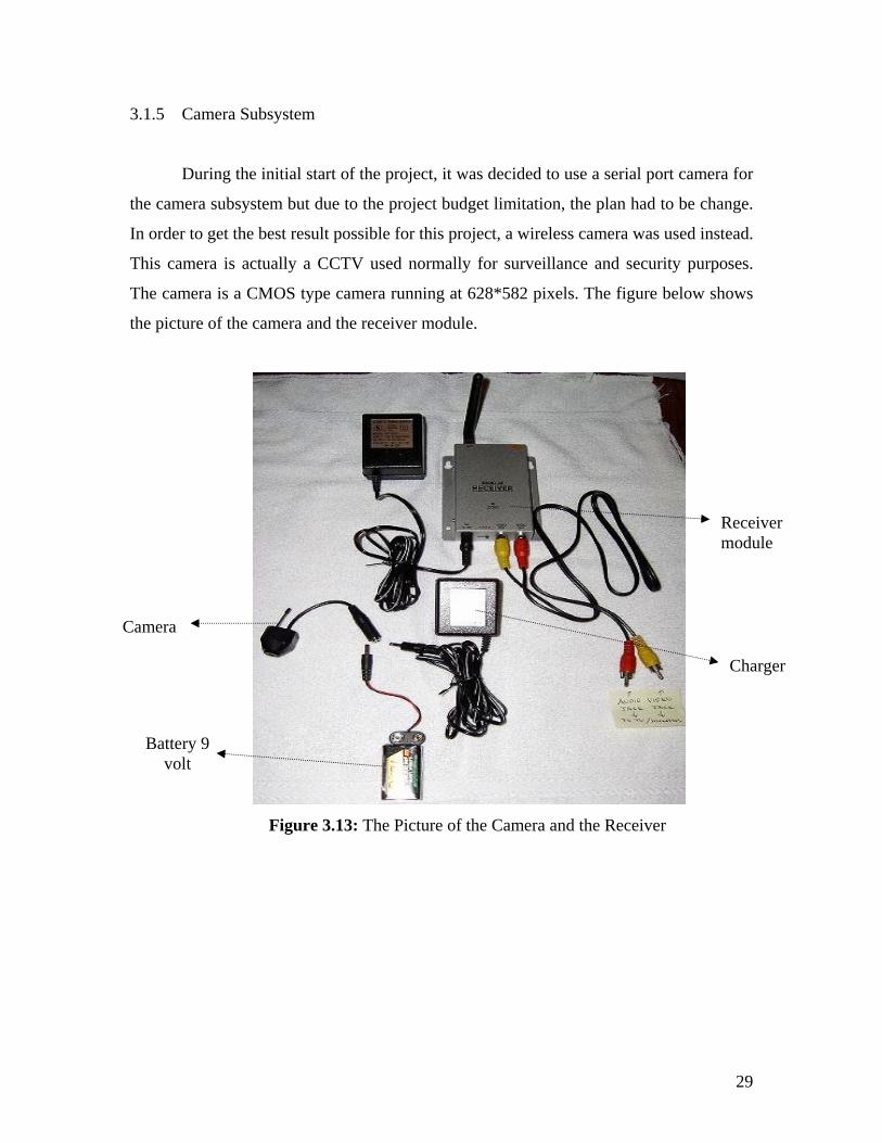
3.1.5 Camera Subsystem
During the initial start of the project, it was decided to use a serial port camera for
the camera subsystem but due to the project budget limitation, the plan had to be change.
In order to get the best result possible for this project, a wireless camera was used instead.
This camera is actually a CCTV used normally for surveillance and security purposes.
The camera is a CMOS type camera running at 628*582 pixels. The figure below shows
the picture of the camera and the receiver module.
Figure 3.13: The Picture of the Camera and the Receiver
Receiver module
Camera
Charger
Battery 9 volt
29
3.1.5.1 Circuit Description of the Camera
Please refer to the Appendix A and B for the schematic diagram. The video signal
from CMOS camera passes through the sharp network(R4, R5, C11,R16), also is added
in the VT of VCO2, another signal is added in the VT of VCO2 is the error voltage
output of loop filter (R1,R24,R25,R28,C17,C19,C25) of PLL(U2) which is programmed
by CPU(U1), the channel data is decided by the encode switch(SW1) of CPU’s
peripheries. The feed back signal (R30, C28) from voltage controlled oscillator VCO2 is
compared with reference crystal oscillator, the error frequency of oscillator VCO2 can be
corrected. The carry frequency modulated of audio & video has been power amplified by
Q2, filtered when through the band pass filter (C20, C18, C23, and micro strip) to make
the higher harmonica of signal reduce to lower level. The purer signal is emitted by
antenna (RFOUT).
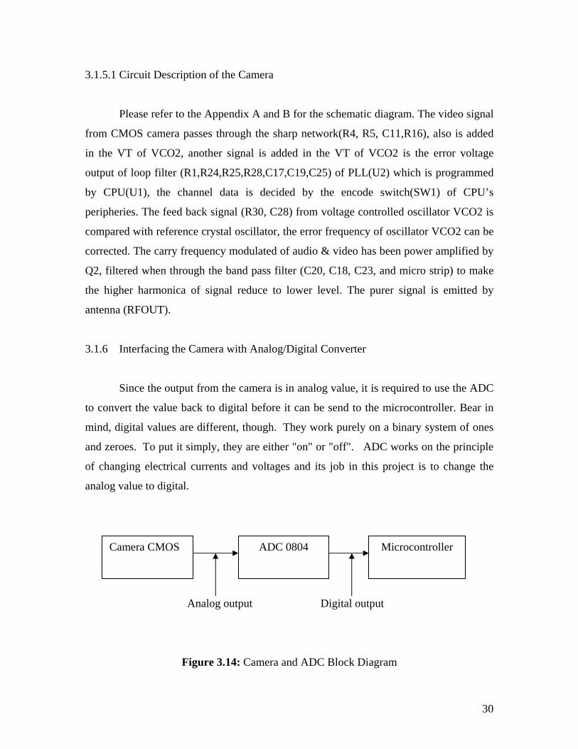
3.1.6 Interfacing the Camera with Analog/Digital Converter
Since the output from the camera is in analog value, it is required to use the ADC
to convert the value back to digital before it can be send to the microcontroller. Bear in
mind, digital values are different, though. They work purely on a binary system of ones
and zeroes. To put it simply, they are either "on" or "off". ADC works on the principle
of changing electrical currents and voltages and its job in this project is to change the
analog value to digital.
Microcontroller ADC 0804 Camera CMOS
Analog output Digital output
Figure 3.14: Camera and ADC Block Diagram
30

3.2 Software Requirement
Software is needed as an interface to control the hardware. The interface for this
project was created using Visual Basic Script. Since the connection is based on serial
port, the Microsoft Comm Component in Visual Basic is used to add a serial
communication to facility. The Communication control provides the following two ways
for handling communications:
• Event-driven: Event-driven communications is the best method of handling
serial communication as it frees the computer to do other things. The events can
be defined as the reception of a character or a change in RTS. The OnComm
event can be used to capture these events and also to detect communications
errors.
• Polling: Commevent properties can be tested to determine if an event or an error
has occurred. For example, the program can loop waiting for a character to be
received. Once received, the character is read from the receive buffer.
In the Visual Basic, to enable the serial port communication, the code below was
written. Explanation for each of the line was given as the following:
MSComm1.CommPort = 1 Open Com 1
MSComm1.Settings = "1200, N, 8, 1" 1200 Baud, No Parity, 8 Data
Bits, 1 Stop Bit
MSComm1.InputLen = 0 Read the entire buffer when
Input is used
MSComm1.PortOpen = True Open Port
31
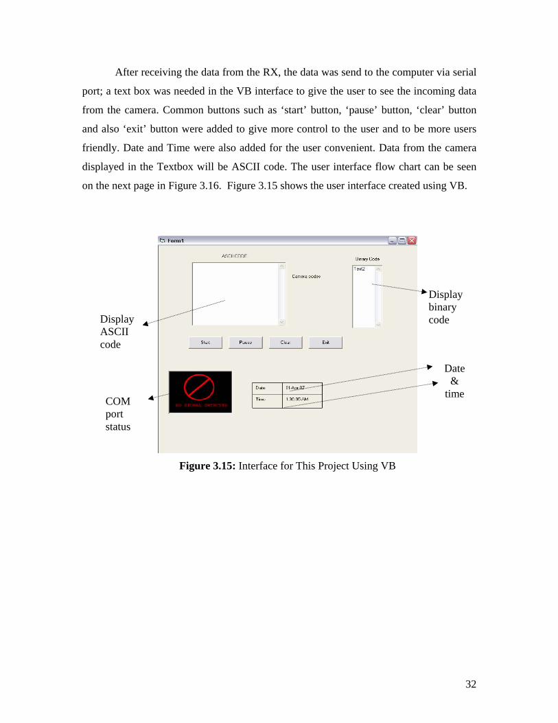
After receiving the data from the RX, the data was send to the computer via serial
port; a text box was needed in the VB interface to give the user to see the incoming data
from the camera. Common buttons such as ‘start’ button, ‘pause’ button, ‘clear’ button
and also ‘exit’ button were added to give more control to the user and to be more users
friendly. Date and Time were also added for the user convenient. Data from the camera
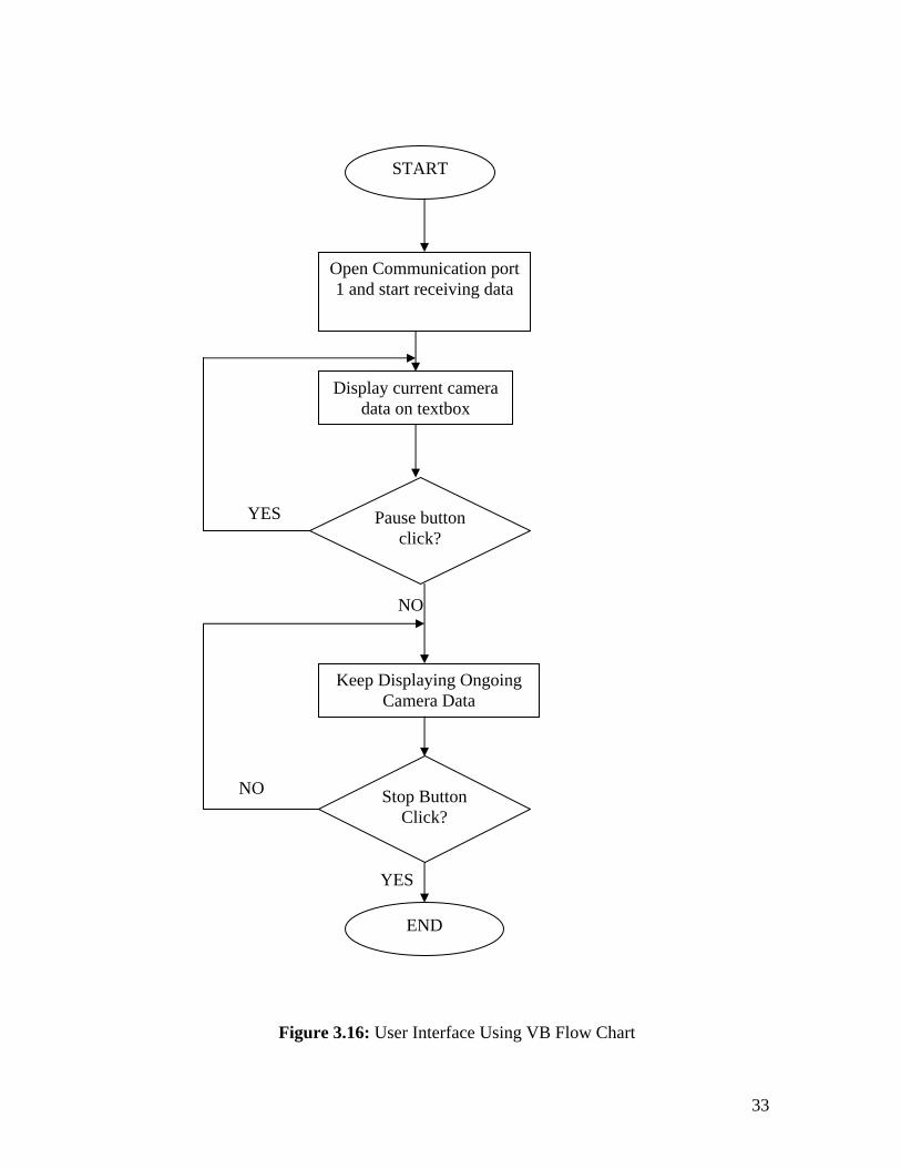
displayed in the Textbox will be ASCII code. The user interface flow chart can be seen
on the next page in Figure 3.16. Figure 3.15 shows the user interface created using VB.
Display binary code Display
ASCII code
Date &
time COM port status
Figure 3.15: Interface for This Project Using VB
32
YES
NO
NO
YES
Figure 3.16: User Interface Using VB Flow Chart
START
Open Communication port 1 and start receiving data
Display current camera data on textbox
Pause button click?
Keep Displaying Ongoing Camera Data
END
Stop Button Click?
33

3.3 Programming the Microcontroller
This section will elaborate on the programming the microcontroller. The
microcontroller used in this project as mentioned in section 3.1.1, is the AT89s52. The
assembler used to assemble the program is the MCS-51 Macro assembler. The program
starts with the configuration of the baud rate. The baud rate used in this program is 1200.
The baud rate was needed to be fixed at 1200 in order to synchronize with the VB
program (Please refer to section 3.2). The microcontroller program is shown as below:
MOV TMOD, #20H ----- use timer 1(T1) in mode 2
MOV TH1, #0E8H ----- to set 1200 baud rate
MOV SCON, #50H ----- use Serial mode1. Enable RX
SETB TR1 ------ start the T1
After the baud rate setting, the next step is to take the information from the serial
port 1(connected to the camera via ADC), and send the data to TX, the TX job is to keep
on sending the data using RF since looping will be done. The program is as shown below:
MOV A, P1 --------- move the receive data from Port 1 to accumulator
CALL SEND --------- send the data via RF
JMP MAIN ---------- to enable infinite loop
As shown on the program above, data will be sent via RF when the ‘CALL
SEND’ line read by the microcontroller. Delay time is needed to synchronize the speed of
transferring data and the speed of receiving data. On the next page, it was shown the
program that involved in the sending the data via RF:
34

SEND:
MOV SBUF, A ---------move the receive byte from accumulator SBUF
WAIT:
JNB TI, WAIT -------- wait until one byte is receive
CLR TI ------- clear T1
CALL DLY -------- delay are needed to slow the speed of sending
data
RET -------- return from subroutine
As can be seen above, the instruction is to wait until 8 bit is transfer and then
check for last bit. If it happens that the one bit is low, it will loop back to WAIT, this is to
check 8 bit was transferred and make sure that the data are send correctly. Figure 3.17 on
the next page shows the program flow for the microcontroller programming.
35

Figure 3.17: Microcontroller Programming Flow Chart
Start
Start to configure the baud rate
Move the Receive Data to Accumulator
Send the data to SBUF From accumulator
No Clear T1 8 bit data receive?
Yes
36


![[ITIL SYSTEM METHODOL OGY ]](https://img.pdfslide.us/doc/110x75/624cd347964d7328d919e9f8/itil-system-methodol-ogy-.jpg)

