Embed Size (px)
Citation preview
Chapter 3
Field Cycling NMR Spectrometer
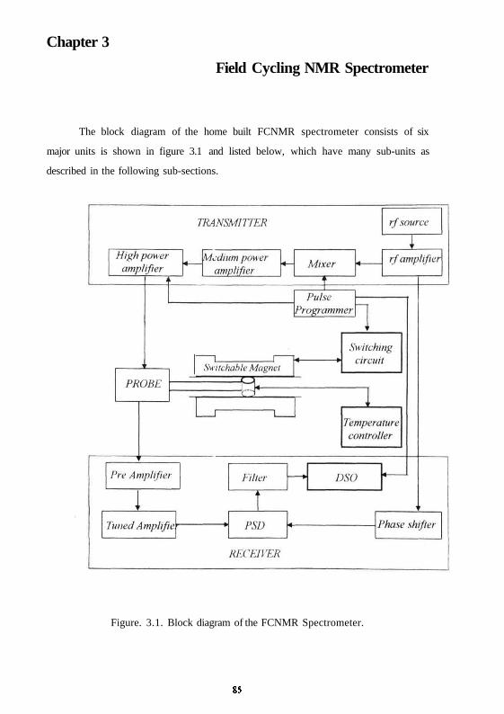
The block diagram of the home built FCNMR spectrometer consists of six
major units is shown in figure 3.1 and listed below, which have many sub-units as
described in the following sub-sections.
Figure. 3.1. Block diagram of the FCNMR Spectrometer.
8̂
> The transmitter gives high power rf pulses, which has mixing and amplifying
circuits.
> The probe for matching the transmitter and receiver, and for providing good S/N
at low frequencies around 3 MHz
> The receiver that could take care of the long dead time and noise problems arising
especially at the low //ranges (around 3 MHz).
> A home built Field Cycling Network, which is already described with its complete
fabrication details in chapter-2.
> A pulse programmer setup which is capable of producing pulses for transmitter,
receiver and for synchronization of field cycling network with the rf pulse
sequences and
> A temperature control facility consisting of a double wall cryostat, heater, air
blower, measurement and control thermocouples and a multimeter
The transmitter should be capable of providing high power rf pulses (typically
in the range of a few hundreds of watts with sharp rising and falling edges) of short
duration (1-100 //sec). The ON/OFF ratio of the //pulses should be very large so as
to ensure that there is no leakage of //voltage into the receiver during the transmitter
OFF time. The //field (Hi) provided by the transmitter should be as homogeneous as
possible, over the sample volume. The transmitter essentially consists of a //source, a
pulse programmer capable of generating the required pulse sequences, a pulsed rf
mixer, a medium power amplifier and a gated high power amplifier.
The power from the transmitter should be efficiently transferred to the spin
system (sample coil) by an impedance matching network. This matching network
along with the sample coil is termed as the probe The signal induced in the sample coil
after the transmitter pulse is very small (typically in //V), and hence, it should be
amplified by the receiver to a few hundred times, and then demodulated to recover the
decaying pattern. Apart from this, the receiver should be capable of withstanding
overload voltages and also recover fast from these voltages (due to leakages during
pulse ON periods). The recovery time of the receiver from overloading should be as
short as possible to ensure that the signal is not lost during this 'dead time' of the
S6
receiver. Moreover, the receiver should be capable of detecting only the carrier wave
in order to increase the signal strength The various sub-units are described in detail
below.
3.1. Transmitter
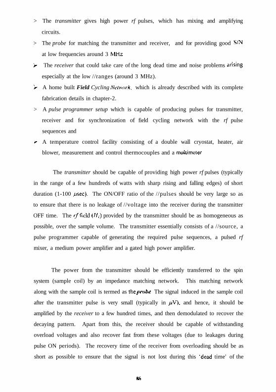
3.1.1. rf generator
The rf voltage obtained from a variable frequency rf synthesizer (commercial
unit of Kikusui make, Model No.4100, capable of generating rf voltage of high
spectral purity, from 0.1 kHz to 110 MHz with a stability of about 1 in 109s), is
amplified using 2N2369 transistors to a required level of about 3 V peak to peak The
//amplifier circuit [73] is shown in figure 3.2.
Figure. 3.2. rf amplifier
The //thus obtained is power divided into two parts, the first part is used for
pulse modulation and the other as reference (through a phase shifter), for the phase
sensitive detector (PSD). The details of the PSD would be discussed later.
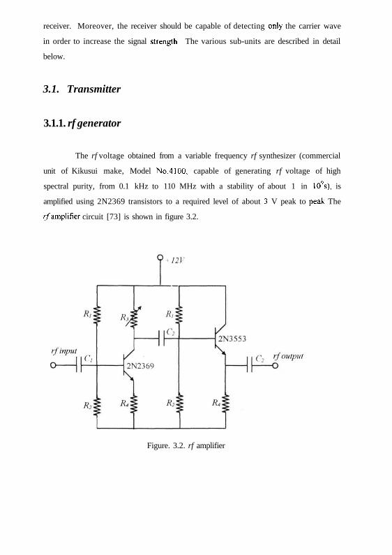
3.1.2. Pulse and delay generators
The pulses and the necessary delays are obtained from a commercial four
channel digital delay generator (EG&G make, Model No.9650) and a homemade pulse
generator [73] panel built using IC74121's. The pulses obtained from these units are
also used for triggering the oscilloscope and the gated high power amplifier. The pulse
generator circuit is shown in figure 3.3. R is the variable resistor and C is the series
capacitor network.
Figure. 3.3. The pulse generator circuit using IC 74121
The required pulses for FCNMR spectrometer (for switching the magnetic field
as well as for the application of the rf pulse sequences) is given in the timing diagram
given in figure. 3.4
88
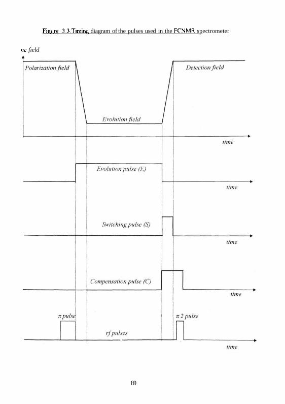
Figure 3.3.Timing diagram of the pulses used in the FCNMR spectrometer
lie field
89
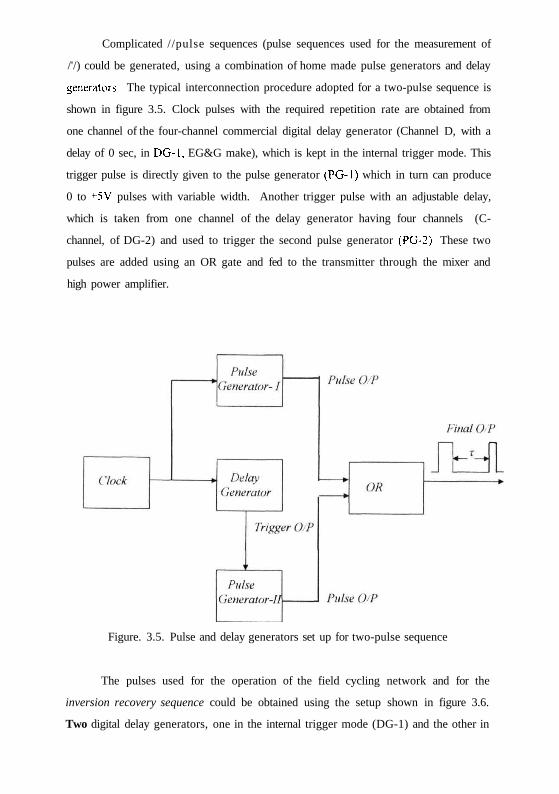
Complicated //pulse sequences (pulse sequences used for the measurement of
/'/) could be generated, using a combination of home made pulse generators and delay
generators The typical interconnection procedure adopted for a two-pulse sequence is
shown in figure 3.5. Clock pulses with the required repetition rate are obtained from
one channel of the four-channel commercial digital delay generator (Channel D, with a
delay of 0 sec, in DG-1, EG&G make), which is kept in the internal trigger mode. This
trigger pulse is directly given to the pulse generator (PG-1) which in turn can produce
0 to +5V pulses with variable width. Another trigger pulse with an adjustable delay,
which is taken from one channel of the delay generator having four channels (C-
channel, of DG-2) and used to trigger the second pulse generator (PG-2) These two
pulses are added using an OR gate and fed to the transmitter through the mixer and
high power amplifier.
Figure. 3.5. Pulse and delay generators set up for two-pulse sequence
The pulses used for the operation of the field cycling network and for the
inversion recovery sequence could be obtained using the setup shown in figure 3.6.
Two digital delay generators, one in the internal trigger mode (DG-1) and the other in
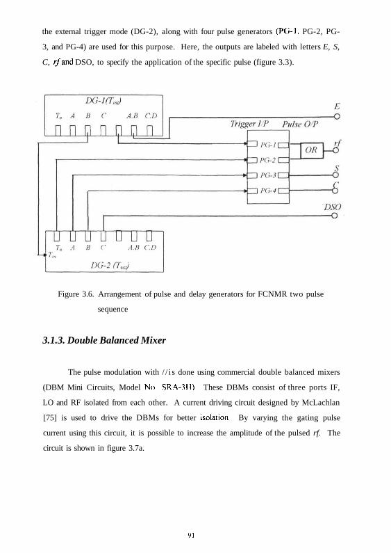
the external trigger mode (DG-2), along with four pulse generators (PG-1, PG-2, PG-
3, and PG-4) are used for this purpose. Here, the outputs are labeled with letters E, S,
C, //and DSO, to specify the application of the specific pulse (figure 3.3).
Figure 3.6. Arrangement of pulse and delay generators for FCNMR two pulse
sequence
3.1.3. Double Balanced Mixer
The pulse modulation with / / i s done using commercial double balanced mixers
(DBM Mini Circuits, Model No SRA-3H) These DBMs consist of three ports IF,
LO and RF isolated from each other. A current driving circuit designed by McLachlan
[75] is used to drive the DBMs for better isolation By varying the gating pulse
current using this circuit, it is possible to increase the amplitude of the pulsed rf. The
circuit is shown in figure 3.7a.
91
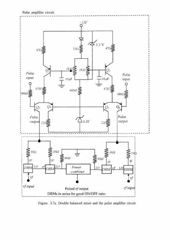
Pulse amplifier circuit
Figure. 3.7a. Double balanced mixer and the pulse amplifier circuit
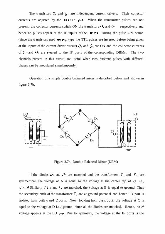
The transistors Q, and Q2 are independent current drivers. Their collector
currents are adjusted by the 1KD trimpot When the transmitter pulses are not
present, the collector currents switch ON the transistors Q4 and Q_<, respectively and
hence no pulses appear at the IF inputs of the DBMs During the pulse ON period
(since the transistors used are pup type the TTL pulses are inverted before being given
at the inputs of the current driver circuit) Q3 and Q4 are ON and the collector currents
of Qi and Q2 are steered to the IF ports of the corresponding DBMs. The two
channels present in this circuit are useful when two different pulses with different
phases can be modulated simultaneously.
Operation of a simple double balanced mixer is described below and shown in
figure 3.7b.
Figure 3.7b. Double Balanced Mixer (DBM)
If the diodes D} and D2 are matched and the transformers T, and T2 are
symmetrical, the voltage at A is equal to the voltage at the center tap of 7). i.e.,
ground Similarly if D$ and D4 are matched, the voltage at B is equal to ground. Thus
the secondary' ends of the transformer T2 are at ground potential and hence LO port is
isolated from both //and If ports. Now, looking from the //port, the voltage at C is
equal to the voltage at D i.e., ground, since all the diodes are matched. Hence, no rf
voltage appears at the LO port Due to symmetry, the voltage at the IF ports is the
same as that, at C and D i.e., zero. Thus, there is no //output at the IF port and
hence, all the three ports are isolated. With the pulses at the IF port and a // signal at
the //port, the current at the IF port rises suddenly during the pulse ON period. This
turns on the diodes and hence the rf appears at the LO port. When the transmitter
pulse is OFF, as explained above, the IF and rf ports are isolated, resulting in a pulse
modulated rf with negligible rise and fall times (less than 0.1 microsecond). Addition
of one more DBMs in the series results in a better ON/OFF ratio and hence a better
S/N at the cost of higher insertion loss.
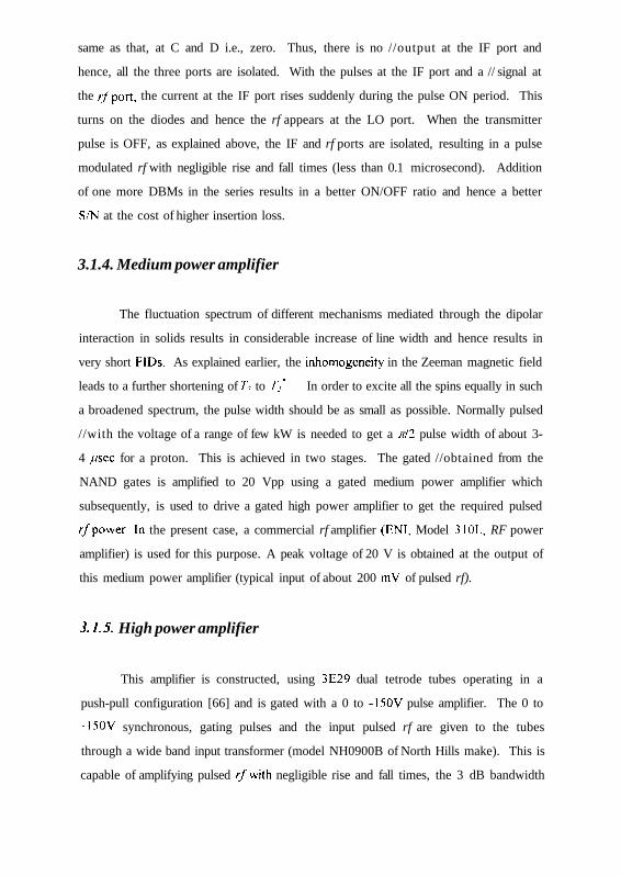
3.1.4. Medium power amplifier
The fluctuation spectrum of different mechanisms mediated through the dipolar
interaction in solids results in considerable increase of line width and hence results in
very short FIDs. As explained earlier, the inhomogeneity in the Zeeman magnetic field
leads to a further shortening of /'? to T2*. In order to excite all the spins equally in such
a broadened spectrum, the pulse width should be as small as possible. Normally pulsed
//with the voltage of a range of few kW is needed to get a irll pulse width of about 3-
4 //sec for a proton. This is achieved in two stages. The gated //obtained from the
NAND gates is amplified to 20 Vpp using a gated medium power amplifier which
subsequently, is used to drive a gated high power amplifier to get the required pulsed
//power. In the present case, a commercial rf amplifier (ENI, Model 310L, RF power
amplifier) is used for this purpose. A peak voltage of 20 V is obtained at the output of
this medium power amplifier (typical input of about 200 mV of pulsed rf).
3.1.5. High power amplifier
This amplifier is constructed, using 3E29 dual tetrode tubes operating in a
push-pull configuration [66] and is gated with a 0 to -150V pulse amplifier. The 0 to
-150V synchronous, gating pulses and the input pulsed rf are given to the tubes
through a wide band input transformer (model NH0900B of North Hills make). This is
capable of amplifying pulsed //with negligible rise and fall times, the 3 dB bandwidth
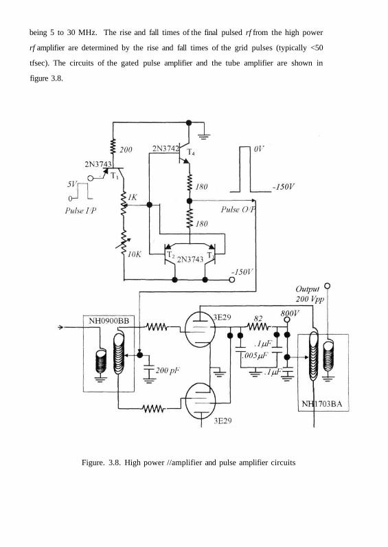
being 5 to 30 MHz. The rise and fall times of the final pulsed rf from the high power
rf amplifier are determined by the rise and fall times of the grid pulses (typically <50
tfsec). The circuits of the gated pulse amplifier and the tube amplifier are shown in
figure 3.8.
Figure. 3.8. High power //amplifier and pulse amplifier circuits
High power amplification and good ON/OFF ratio is accomplished by biasing
the grids of the dual tetrodes with OV during pulse ON period and -150V during the
pulse OFF period. The working of the pulse amplifier can be understood as follows.
During the pulse OFF period, the transistor Ti is OFF, resulting in -150V at the bases
of T2, T3 and T4. Since both, the/;///; transistors T2 and T3 are conducting and the npn
transistor, T4 is not conducting, -150V appears at the grids of the tubes. Thus, during
the pulse OFF period, no amplification is done resulting in an improved ON/OFF ratio.
During the pulse ON period, Ti conducts making the voltage at the base of T2, T3 and
T4 from -150V to OV Thus T2 and T? are OFF and T4 is ON, resulting in OV at the
grids of the tubes The output of the amplifier is taken through another wide band
transformer (North Hills NH1703BA). Since the plates of the tetrodes are at about
800V, very high amplification (-10) of the input pulsed / / i s achieved during the pulse
ON period.
96
3.2. Matching network
The most important part of a pulsed NMR spectrometer is the matching
network (probe) which couples the power from the transmitter to the sample coil
during the pulse ON period and converts the precessing magnetization into a
detectable signal at the input of the receiver immediately following the pulse. The
matching network should be capable of coupling the sample coil to the transmitter
during the pulse ON period and should also couple the sample coil to the receiver
during the pulse OFF period. It should also decouple the receiver from the transmitter
during the pulse ON period The important considerations during the construction of
the probe are discussed here. The amplitude of Hl and hence the w'2 pulse width, is
determined by the transmitter coil and the final S/N is determined by the sensitivity of
the receiver coil One crucial factor in the design of the size of the sample is that, since
Hjoc(y/1/2, where V is the effective volume of the sample, a probe built for a larger
sample would have a smaller H, for the sample power. Moreover, for a good signal to
noise ratio (S N oc(f) ' '\ where/is the filling factor of the coil), it is necessary that the
probe should have a filling factor close to unity. Finally, the receiver coil in the probe
should not give rise to spurious signals (for example, from the mechanical oscillations
of the inadequately secured rfcoW or generation of acoustic waves and signals, which
interfere with the actual signals).
The above requirements can be fulfilled by using tunable circuits consisting of
LCR networks Either the crossed coil method [67] proposed by Bloch et al., where
separate transmitter and receiver coils are used or the single coil method [68,69]
proposed by Clark and McNeil, where a single coil is used for both the transmitter and
the receiver, can be used for this purpose. The single coil arrangement is simpler and
has advantages over the other one in terms of the maximum power efficiency. Since
the coil is common to both the transmitter and the receiver, care should be taken to
protect the receiver from leakage of rf pulses from the transmitter, i.e. the probe
should isolate the receiver from the transmitter. This can be achieved by using crossed
diodes and k/4 transmission lines which appear as short-circuit to high voltages and
open circuit to the small signals. Two matching circuits available in the literature are
used in the present studies and their relative merits are discussed here. Both the circuits
are single coil circuits, which are easier to handle, and also efficient compared to the
crossed coil probe.
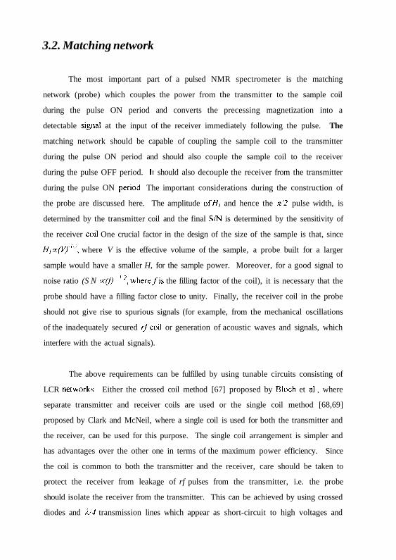
3.2.1. Series resonant circuit
This matching network [68] consists of three resonant circuits, L/C/, L2C2 and
L3C3 each tuned independently at the Larmor frequency (Figure.3.9).
Figure 3.9. Series resonant circuit [68]
The crossed diodes (D/) at the input act as a short circuit to the small signal voltages
(during pulse OFF period). The series combination, L2C2 represents a low impedance
path in parallel with that of L3C3 so that the entire transmitter voltage is dropped
across L2 and a very little voltage is fed into the receiver during the pulse ON period.
Moreover, since the diode pair (Di) represents short circuit to ground, the voltage at E
is dropped across L3 before reaching the receiver. After the transmitter pulse, the
diode pair Dt effectively disconnects it from E and D2 acts as an open circuit to the
low voltage induced resonant signals, thereby forcing the signal into the receiver
through L3C3. Hence, L2C2 and L3C3 represent a composite series circuit tuned at the
Larmor frequency. The FID is received at F (a high impedance point to ground). The
tuned input receiver circuit (L3C3) provides a good coupling of L2 to the receiver and
hence increases the S/N. Thus, the circuit ensures an efficient transfer of power from
the transmitter to the sample coil and also a good protection of the receiver from
destructive overloads.
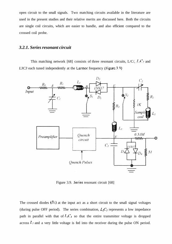
3.2.2. Parallel resonant circuit
Figure. 3.10. Parallel resonant circuit [69]
The second circuit [69], given in figure 3.10, which consists of a series
resonant tank circuits (L1C1), in series with a capacitor CY The crossed diodes at the
input of the circuit allow the high power rf voltages to pass through the sample coil,
99
while acting as an open circuit to the small signals induced in the coil. The diodes at
the output of the circuit allow any //power leaked into the ground, thus protecting the
receiver from the rf pulses, while acting as open circuit to the small NMR signals,
thereby forcing them to pass entirely into the receiver. These crossed diodes also
remove low level noise and other transients originating in the transmitter and hence
improve the S/N of the system. In addition, the presence of the quarter wave network
before the diode pair offers high impedance for transmitter pulses thus protecting the
receiver from further overload [77]. The input and output impedances of the tuned
coil is chosen to be equal to 50 Ohms. C2 is chosen to be as small as possible in order
to minimize the degradation of the L/C ratio and in turn the quality factor Q of the
circuit. The conditions for tuning the circuit are given by [77] the equations 3.72.
Here, Q is the quality factor of the coil which is made as large as possible to
optimize the S/N and power transfer efficiency. On the other hand, a very large Q
would result in a long ringing time and hence, a long dead time of the receiver, even
after the turn OFF of the rf Hence for broad signals, it is advantageous to reduce Q at
the cost of a lower S/N. L is determined from equation 3.72b and C\ from equation
3.72a. The tuning of the circuit is done by slowly changing the values of the circuit
elements, for maximum power at the coil. Fine tuning can be done further, by
observing the ringing pattern after the pulse. The k\4 circuit acts as the impedance
transformer network. When shorted at one end, the X\4 line transmits the low voltage
signals at the designed frequency and hence attenuates all other frequencies (equivalent
to a selective filter).
Two different types of X\4 networks are used [77] depending on the recovery
time requirements. The first one consists of an inductor L3, and two capacitors C3
(3.72a)
(3.72b)
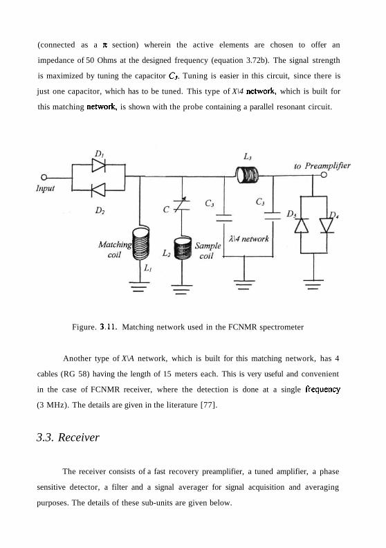
(connected as a n section) wherein the active elements are chosen to offer an
impedance of 50 Ohms at the designed frequency (equation 3.72b). The signal strength
is maximized by tuning the capacitor Cj. Tuning is easier in this circuit, since there is
just one capacitor, which has to be tuned. This type of X\4 network, which is built for
this matching network, is shown with the probe containing a parallel resonant circuit.
Figure. 3.11. Matching network used in the FCNMR spectrometer
Another type of X\A network, which is built for this matching network, has 4
cables (RG 58) having the length of 15 meters each. This is very useful and convenient
in the case of FCNMR receiver, where the detection is done at a single frequency
(3 MHz). The details are given in the literature [77].
3.3. Receiver
The receiver consists of a fast recovery preamplifier, a tuned amplifier, a phase
sensitive detector, a filter and a signal averager for signal acquisition and averaging
purposes. The details of these sub-units are given below.
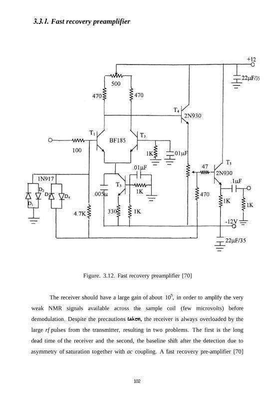
3.3.1. Fast recovery preamplifier
Figure. 3.12. Fast recovery preamplifier [70]
The receiver should have a large gain of about 105, in order to amplify the very
weak NMR signals available across the sample coil (few microvolts) before
demodulation. Despite the precautions taken, the receiver is always overloaded by the
large rf pulses from the transmitter, resulting in two problems. The first is the long
dead time of the receiver and the second, the baseline shift after the detection due to
asymmetry of saturation together with ac coupling. A fast recovery pre-amplifier [70]
102
is used to overcome these problems. The circuit diagram of the fast recovery
preamplifier is shown in figure 3.12. The values of the resistors in Ohms are given
adjacent to the resistors.
The preamplifier possesses high sensitivity and short recovery times, besides a
large bandwidth. The dc level of the feedback circuit is adjusted by a variable resistor
(10 K) such that the positive and negative limit of the rf pulses are symmetric about the
baseline. The gain is adjusted to about 10 and a bandwidth from 1 kHz to 15 MHz.
The diodes Di and D2 protect the input of the receiver from large //pulses. The diodes
D3 and D4 in the feed back circuit limit the high voltage rf pulses to the receiver to a
very low value (less than ±0.5V).
3.3.2. Tuned Amplifiers
A narrow band double tuned amplifier (Matec Make, Model: 252) and a tuned
amplifier (Matec make, Model: 625) are used to amplify the signal coming from the
fast recovery preamplifier. The output of these amplifier stages is fed to a PSD.
3.3.3. PSD and phase shifter
The amplified NMR signal from the probe consists of all frequency
components, along with the frequency of interest, and hence has to be demodulated
before signal averaging. The Phase Sensitive Detector (PSD) has a shorter bandwidth
and hence a better S/N [71] than the other detectors such as the diode detector. Since,
PSD is sensitive to the phase of the signal, it is useful in obtaining phase information
also. A commercial double balanced mixer (DBM) is used as a PSD in the present
case. The signal of frequency /, is applied at the LO port of the DBM (HP make,
Model No. 10534A). The reference rf, with frequency f0 is fed into the / /port . The
detected output, which is proportional to the frequency f+f0 and the difference of the
frequencies of the two inputs, fo-f is taken out from the IF port of the DBM. Thus,
when the frequency of the reference is same as the signal, an output, corresponding to
zero frequency is obtained. The signal strength is further maximized by decreasing the
103
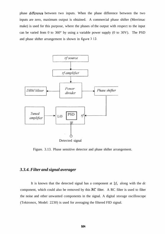
phase difference between two inputs. When the phase difference between the two
inputs are zero, maximum output is obtained. A commercial phase shifter (Merrimac
make) is used for this purpose, where the phases of the output with respect to the input
can be varied from 0 to 360° by using a variable power supply (0 to 30V). The PSD
and phase shifter arrangement is shown in figure.3.13.
Detected signal
Figure. 3.13. Phase sensitive detector and phase shifter arrangement.
3.3.4. Filter and signal averager
It is known that the detected signal has a component at 2f0 along with the dc
component, which could also be removed by this RC filter. A RC filter is used to filter
the noise and other unwanted components in the signal. A digital storage oscilloscope
(Tektronox, Model: 2230) is used for averaging the filtered FID signal.
104
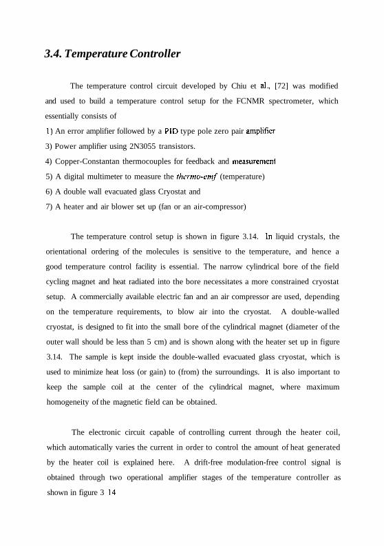
3.4. Temperature Controller
The temperature control circuit developed by Chiu et al., [72] was modified
and used to build a temperature control setup for the FCNMR spectrometer, which
essentially consists of
1) An error amplifier followed by a PID type pole zero pair amplifier
3) Power amplifier using 2N3055 transistors.
4) Copper-Constantan thermocouples for feedback and measurement
5) A digital multimeter to measure the thermo-emf (temperature)
6) A double wall evacuated glass Cryostat and
7) A heater and air blower set up (fan or an air-compressor)
The temperature control setup is shown in figure 3.14. In liquid crystals, the
orientational ordering of the molecules is sensitive to the temperature, and hence a
good temperature control facility is essential. The narrow cylindrical bore of the field
cycling magnet and heat radiated into the bore necessitates a more constrained cryostat
setup. A commercially available electric fan and an air compressor are used, depending
on the temperature requirements, to blow air into the cryostat. A double-walled
cryostat, is designed to fit into the small bore of the cylindrical magnet (diameter of the
outer wall should be less than 5 cm) and is shown along with the heater set up in figure
3.14. The sample is kept inside the double-walled evacuated glass cryostat, which is
used to minimize heat loss (or gain) to (from) the surroundings. It is also important to
keep the sample coil at the center of the cylindrical magnet, where maximum
homogeneity of the magnetic field can be obtained.
The electronic circuit capable of controlling current through the heater coil,
which automatically varies the current in order to control the amount of heat generated
by the heater coil is explained here. A drift-free modulation-free control signal is
obtained through two operational amplifier stages of the temperature controller as
shown in figure 3 14.
Figure. 3.14. Temperature controller and Cryostat arrangement
The first stage of the circuit acts as a simple error amplifier. This takes the
input reference signal through a 10 turn calibrated helipot, and the thermo-emf sensed
by the thermo couple junction kept on the sample tube. The difference (error) is
106
amplified and any variation in the set temperature would be removed by increasing or
decreasing the current through the heater coil.
The second stage, which is a PID type pole-zero amplifier designed for the
field-cycling control circuit, is found to be very useful here. A modulation free control
signal is obtained using this, which in turn is fed to the bases of the power transistors.
When the reference voltage is more than the sensor voltage, a positive voltage appears
at the output of the error amplifier, thereby turning ON the power transistors. This
leads to an increase in the current flowing through the heater coil and hence, the
temperature increases to the set value. The increase in the sensor voltage reduces the
difference at the inputs of the error amplifier, thus making the output of the error
amplifier less positive and less current pass through the heater coil. This heating
decreases once the temperature is higher than the required value. This increase and
reduction of heating, controls the temperature to stay at a constant value. Apart from
the thermal mass inside the cryostat there are other factors like the rate of airflow,
position of the sensor, and the position of the heater coil, are crucial for the good
performance of the temperature controller A temperature stability of 0.2 K within the
time about 30 minutes is obtained
3.5. Automation
The FCNMR spectrometer is connected to a PC through IEEE488 interface
bus for automatic controlling of the spectrometer for data transfer. A digital storage
oscilloscope and the delay generators are also interfaced with the PC for signal
averaging and measurement of FID amplitudes.
Conclusions of the unit -1
> A simple Field Cycling Network capable of providing reasonable field cycling is
achieved.
> Some of the important units were built for the transmitter, receive, probe and
temperature controller and partially automated with the help of a computer. Thus
FCNMR spectrometer capable of operating at a detection frequency of about 3
MHz is fabricated and standardized.
> The performance of the spectrometer was tested by measuring 1) values in
standard samples.
r The FCNMR spectrometer has been routinely used for collecting, proton T\ data as
a function of frequency and temperature, in liquid crystals. Spin-lattice relaxation
time experiments had been performed on the homologous series 40.m,
(butyloxybenzylidene alkylanilines) as a part of this Ph. D thesis. The results are
presented in chapter-6 A binary mixture of liquid crystals, 8CN and 7BCB has
been studied and the results are presented in chapter-7. FCNMR spectrometer has
been used by other researchers [78,79] in the same laboratory, for the frequency
and temperature dependent T\ measurements in liquid crystals.
r It is important to mention that, the conventional NMR spectrometer available in
this laboratory, which is capable of providing proton T] from 3 MHz to 50 MHz
enhances the time window by another decade. The Tt data collected at 3 MHz
using both the spectrometers is useful to understand the functioning of the
FCNMR spectrometer and the reliability of the NMRD data. The specifications of
the spectrometers (FCNMR and NMR) are given in the tables 1 and 2.
I0X
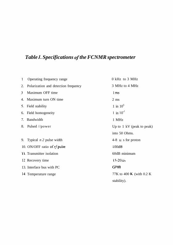
Table L Specifications of the FCNMR spectrometer
1. Operating frequency range
2. Polarization and detection frequency
3 Maximum OFF time
4. Maximum turn ON time
5. Field stability
6. Field homogeneity
7. Bandwidth
8. Pulsed //power
9. Typical n 2 pulse width
10. ON/OFF ratio of//pulse
11. Transmitter isolation
12 Recovery time
13. Interface bus with PC
14. Temperature range
0 kHz to 3 MHz
3 MHz to 4 MHz
1 ms
2 ms
1 in 105
1 in 10'5
1 MHz
Up to 1 kV (peak to peak)
into 50 Ohms.
4-8 u, s for proton
lOOdB
60dB minimum
15-20 u.s
GPIB
77K to 400 K (with 0.2 K
stability).
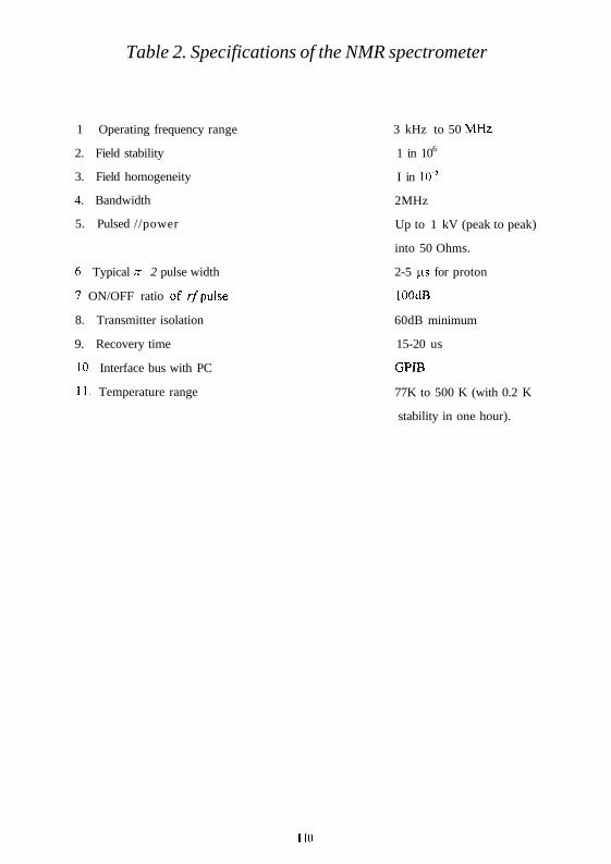
Table 2. Specifications of the NMR spectrometer
1 Operating frequency range
2. Field stability
3. Field homogeneity
4. Bandwidth
5. Pulsed //power
6 Typical re. 2 pulse width
7 ON/OFF ratio of A/pulse
8. Transmitter isolation
9. Recovery time
10. Interface bus with PC
11. Temperature range
3 kHz to 50 MHz
1 in 106
I in 10"5
2MHz
Up to 1 kV (peak to peak)
into 50 Ohms.
2-5 us for proton
lOOdB
60dB minimum
15-20 us
GPIB
77K to 500 K (with 0.2 K
stability in one hour).
no
References for the Unit - /
1 R V. Pound, Phys. Rev. 81, 156 (1951).
2 Schumacher, Phys. Rev. 112, 837 (1958).
3. A. Abragam and W. G. Proctor, Phys. Rev. 109, 1441 (1954).
4 P. S. Pershan, Phys. Rev. 117, 109 (1960).
5 B C Johnson and W. I Goldberg, Phys. Rev. 145, 380 (1966).
6. G P. Jones, J. T. Daycock, and T T. Roberts. ./. Phys. E (Sci. Just) 2, 630 (1968)
7 R Blinc, M. Luzar, M Mali, R Osredkar, J. Seliger and M Vilfan, ./. Physique
Colloque 37, C3-73 (1976)
8 D T Edmonds, Phys. Rep. 29, 233 (1977).
9. M. Packard and R. Varian Phys. Rev. 93, 941(1954).
10 A. Bloom and D. Mansir, Phys. Rev. 94, 41 (1954)
11 A. G Redfield, W. Fite and H. E. Bleich, Rev. Sci. Just. 39, 710 (1968).
12. F. Noack l NMR Field Cycling spectroscopy - principles and applications' in
Progress in NMR Spectroscopy, 18, 171 (1986), and references therein.
13. E. Rommel, K. Mischker, G Osswald, K. H Schweikert and F. Noack, J. Mag.
Res. 70,219(1986).
14. T. P. Das, and E L Hahn, Solid State Physics, Suppl /, Academic Press, New
York (1958).
15 L. C. Hebel and C. P. Slichter, Phys. Rev. 113, 1504 (1959)
16. Y. Masuda and A G. Redfield, Phys. Rev. 125, 159 (1962).
17. Y. Masuda and A. G. Redfield, Phys. Rev. 133A, 944 (1964).
18 A. G. Redfield, Phys. Rev. 130, 589 (1963).
19. A. G. Redfield, Phys. Rev. 162, 367 (1967)
20 R. E. Slusher and E. L. Hahn, Phys. Rev. 116, 332 (1968).
21 D T. Edmonds, Bull. Mag. Res. 3, 53 (1981).
22. P. Van Hecke and G. Jannsens, Phys. Rev. B17, 2124 (1978)
23 P. Coppen, L Van Gerven, S. Clough and A. J. Horsewill, J. Phys. C 16, 567
(1983).
24 M Perger, A. M. Raaen and 1. Svare, ./. Phys. C16, 181 (1983).
25 K. H. Schweikert, Ph. I) Thesis, Universitat Stuttgart, Germany (1990).
26. I. Solomon, Phys. Rev. 99, 559 (1955).
27 1. Solomon and N. Bloembergen,./. Chem. Phys. 25, 261 (1956).
28 J. Seliger, R Orsedgar, M Mali and R. Blinc, ./. Chem. Phys. 65, 2887 (1976).
29 S H. Koenig, R. G. Bryant, K. Hallenga and G. S. Jacob, Biochemistry, 17, 4348
(1978).
30. M. Vilfan, J. Seliger, V. Zagar and R. Blinc, Phys. Lett. 79 A, 186 (1980).
3 1. F. Winter and R. Kimmich, Mol. Phys. 45, 33(1982)
32. F Winter and R. Kimmich, Biochem Biophys. Ada 719, 292 (1982).
33 R. Blinc, M. Vilfan and J Seliger, Bull. Magn. Res. 5, 51 (1983).
34 J. Dolinsek, T. Apih and R. Blinc,./. Phys. Cond. Matter 4, 7203 (1992).
35. R. Kimmich, Bull. Magn. Res. 1, 195 (1980).
36. R. Kimmich, "NMR: Tomography, Diffusometry, Relaxometry", Heidelberg:
Springer-Verlog (1997), and references therein.
37 Proceedings of the "Field Cycling NMR Relaxometry - Symposium", Berlin
(1998).
38. R Zamer, E. Anoardo, O Mensio, D. Pusiol, S Becker and F Noack in
"Field Cycling NMR Relaxometry - Symposium ", Berlin, p92 (1998).
39. A. G. Krushelnitsky, D. V. Markov, A.A. Kharitonov, A. E. Mefeld and V D
Fedotov in "Field Cycling NMR Relaxometry - Symposium ", Berlin, 20 (1998)
40. D. J. Pusiol and E. Anoardo, in "Field Cycling NMR Relaxometry - Symposium",
Berlin, 29(1998).
41 J. Struppe, T. Liesener, F. Noack and M. Vilfan in "Field Cycling NMR
Relaxometry - Symposium ". Berlin, 32 (1998).
42 J. Kryzystek, M. Notter, and A. L. Kwiram,./. Phys. Chem. 98, 3559 (1995).
43. G. Sturm, D. Killian, A. Lotz and J. Voitlander in "Field Cycling NMR
Relaxometry - Symposium ", Berlin, 86 (1998).
44 C. Job, J. Zajicek and M. F. Brown, Rev. Sci. Instrum. 67(6), 2113 (1996).
45. G. Scauer, W. Nusser, M. Blanz, and R. Kimmich J. Phys. E: Sci Instrum 20, 43
(1987)
46 M. Blanz, T J Rayner, J. A. S. Smith, Meas. Sci. Technol., 4, 48 (1993).
47 G. Grossel, F Winter and R. Kimmich,./. Phys. E: Sci Instrum 18, 358 (1985).
112

48. G. R. Kumar, P. Chaddah, Cryogenics 27, 229 (1987).
49. K. H. Schweikert, R. Krieg and F. Noack, ./. Magn. Reson 78, 77 (1988)
50. A. G. Redfield, W. Fite and H E Bleich, Rev. Sci. lust. 39, 710 (1968)
51. R. Kimmich and F. Noack Z. Nafurforsch 25a, 1680, (1970).
52. R. D. Brown and S H. Koenig, IBM Research Rep. RC6712, York Town
Heights (1977).
53. W. Wolfel, Ph. D Thesis, Universitat Stuttgart, Germany (1978).
54. V. Graf Ph. 1) Thesis, Universitat Stuttgart, Germany (1980).
55. G. Voigt and R. Kimmich, Polymer, 21, 1001 (1980).
56. J. Hak, Arch. Electroteck 30, 736 (1936).
57. D. B. Montgomery, Solenoid Magnet Design, Wiley, New York (1969)
58. L.Cesnak and D. Kabat,./. Phys (E) 5, 944 (1972).
59. G. Grossel, F. Winter and R Kimmich,./. Phys. E: Sci lnstrum 18, 358 (1985)
60. M. Packard, R. Varian, A Bloom and D. Mansir Phys. Rev. 93, 941 (1954).
61. C. W. Lander, Power Electronics, McGraw-Hill, New York (1981).
62. O. Feustel and W. Schmidt, Scnsorhalbleiter undSchuizelemente\ Vogel Verlog,
Wurzburg (1982)
63. H. Buri, Leistungshalbleiter, Brown, Boverie and Cie, Mannheim (1983)
64. M. Kubat, Power Semiconductors, Springer, Berlin (1984)
65. R. Felderhoff, Leistungselektronik, Hansor, Munchen (1984).
66. 1. J. Lowe and C. E. Tarr, J Phys., El,320 (1968).
67. F. Bloch , Phys. Rev 70,460, (1946).
68 W. G. Clark and J. A. McNeil, Rev. Sci. lnstrum , 44, 844 (1973).
69. D. C. Ailion, " Methods of Solid State Physics", ed., J. N. Mundy, S. J. Rothman,
K. H. Fluss, and L. C. Sumedskjaer (Academic Press ) 21, 439 (1983).
70. B. Ramadan, Ng. T. C. and E Tward, Rev. Sci. lust., 45, 1174 (1974).
71. T. C. Farrar and E. D. Becker, 'Pulse and FT NK4R', Academic Press, New York
(1971)
72. U. T. H. Chiu, D. Griller, K. V. lngold, and P. Knittel,./. Phys. E12, 274 (1979)
73. K. Venu, Ph. D thesis, University of Hyderabad, India (1986).
74. A. S. Sailaja, Ph.D Thesis, University of Hyderabad, India (1994); A. S. Sailaja,
D. Loganathan and K. Venu, Proc. hid. Acad. Sci. India, 66(A), 161 (1996).
75. McLachlan,./. Magn. Reson., 47, 490 (1982).
76 T. Jeener and P. Broekaert, Phys. Rev., 157, 232 (1967).
77 E Fukushirna and S. B. W. Roeder, 'Experimental PulsedNMR-A nuts and bolts
approach', Addison Wesley, Reading, Massachusetts (1981).
78 M. Venkata Reddy, M. Phil Thesis, University of Hyderabad, Hyderabad India
(1999).
79. V. Satheesh, Ph. D Thesis, University of Hyderabad, Hyderabad, India (2000).
114