Embed Size (px)
Citation preview
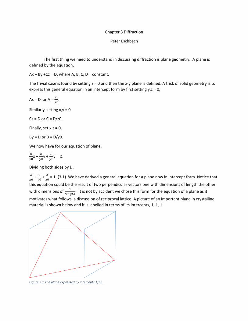
Chapter 3 Diffraction
Peter Eschbach
The first thing we need to understand in discussing diffraction is plane geometry. A plane is
defined by the equation,
Ax + By +Cz = D, where A, B, C, D = constant.
The trivial case is found by setting z = 0 and then the x-y plane is defined. A trick of solid geometry is to
express this general equation in an intercept form by first setting y,z = 0,
Ax = D or A = 𝐷
𝑥0.
Similarly setting x,y = 0
Cz = D or C = D/z0.
Finally, set x.z = 0,
By = D or B = D/y0.
We now have for our equation of plane,
𝐷
𝑥0x +
𝐷
𝑦0y +
𝐷
𝑦0y = D.
Dividing both sides by D,
𝑥
𝑥0 +
𝑦
𝑦0 +
𝑧
𝑧0 = 1. (3.1) We have derived a general equation for a plane now in intercept form. Notice that
this equation could be the result of two perpendicular vectors one with dimensions of length the other
with dimensions of 1
𝑙𝑒𝑛𝑔𝑡ℎ. It is not by accident we chose this form for the equation of a plane as it
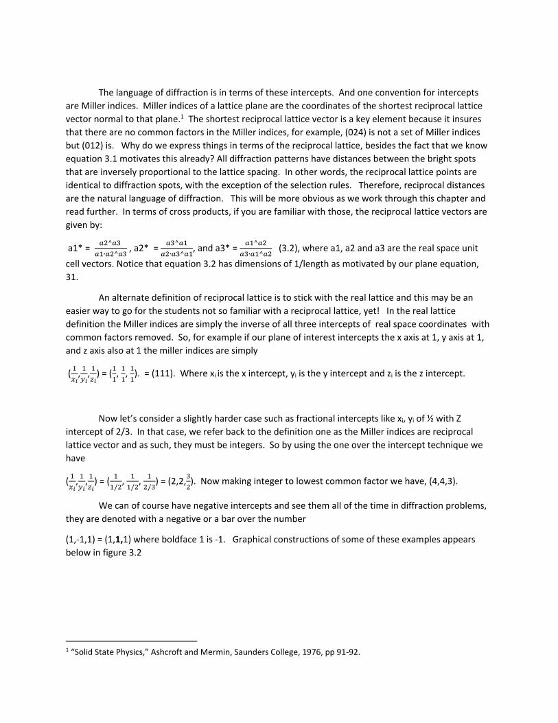
motivates what follows, a discussion of reciprocal lattice. A picture of an important plane in crystalline
material is shown below and it is labelled in terms of its intercepts, 1, 1, 1.
Figure 3.1 The plane expressed by intercepts 1,1,1.
The language of diffraction is in terms of these intercepts. And one convention for intercepts
are Miller indices. Miller indices of a lattice plane are the coordinates of the shortest reciprocal lattice
vector normal to that plane.1 The shortest reciprocal lattice vector is a key element because it insures
that there are no common factors in the Miller indices, for example, (024) is not a set of Miller indices
but (012) is. Why do we express things in terms of the reciprocal lattice, besides the fact that we know
equation 3.1 motivates this already? All diffraction patterns have distances between the bright spots
that are inversely proportional to the lattice spacing. In other words, the reciprocal lattice points are
identical to diffraction spots, with the exception of the selection rules. Therefore, reciprocal distances
are the natural language of diffraction. This will be more obvious as we work through this chapter and
read further. In terms of cross products, if you are familiar with those, the reciprocal lattice vectors are
given by:
a1* = 𝑎2^𝑎3
𝑎1∙𝑎2^𝑎3 , a2* =
𝑎3^𝑎1
𝑎2∙𝑎3^𝑎1, and a3* =
𝑎1^𝑎2
𝑎3∙𝑎1^𝑎2 (3.2), where a1, a2 and a3 are the real space unit
cell vectors. Notice that equation 3.2 has dimensions of 1/length as motivated by our plane equation,
31.
An alternate definition of reciprocal lattice is to stick with the real lattice and this may be an
easier way to go for the students not so familiar with a reciprocal lattice, yet! In the real lattice
definition the Miller indices are simply the inverse of all three intercepts of real space coordinates with
common factors removed. So, for example if our plane of interest intercepts the x axis at 1, y axis at 1,
and z axis also at 1 the miller indices are simply
(1
𝑥𝑖,
1
𝑦𝑖,
1
𝑧𝑖) = (
1
1,
1
1,
1
1). = (111). Where xi is the x intercept, yi is the y intercept and zi is the z intercept.
Now let’s consider a slightly harder case such as fractional intercepts like xi, yi of ½ with Z
intercept of 2/3. In that case, we refer back to the definition one as the Miller indices are reciprocal
lattice vector and as such, they must be integers. So by using the one over the intercept technique we
have
(1
𝑥𝑖,
1
𝑦𝑖,
1
𝑧𝑖) = (
1
1/2,
1
1/2,
1
2/3) = (2,2,
3
2). Now making integer to lowest common factor we have, (4,4,3).
We can of course have negative intercepts and see them all of the time in diffraction problems,
they are denoted with a negative or a bar over the number
(1,-1,1) = (1,1,1) where boldface 1 is -1. Graphical constructions of some of these examples appears
below in figure 3.2
1 “Solid State Physics,” Ashcroft and Mermin, Saunders College, 1976, pp 91-92.
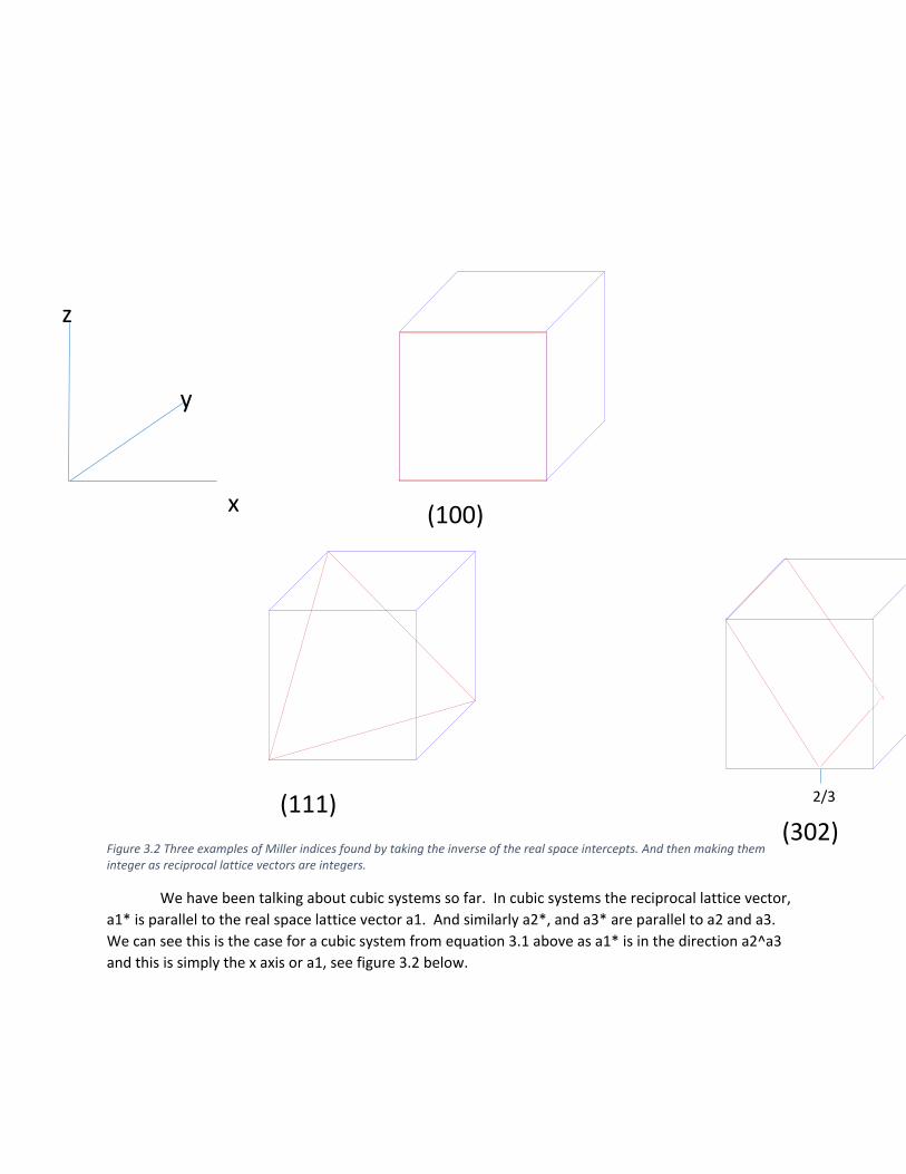
Figure 3.2 Three examples of Miller indices found by taking the inverse of the real space intercepts. And then making them integer as reciprocal lattice vectors are integers.
We have been talking about cubic systems so far. In cubic systems the reciprocal lattice vector,
a1* is parallel to the real space lattice vector a1. And similarly a2*, and a3* are parallel to a2 and a3.
We can see this is the case for a cubic system from equation 3.1 above as a1* is in the direction a2^a3
and this is simply the x axis or a1, see figure 3.2 below.
(111)
z
x
y
2/3
(100)
(302)
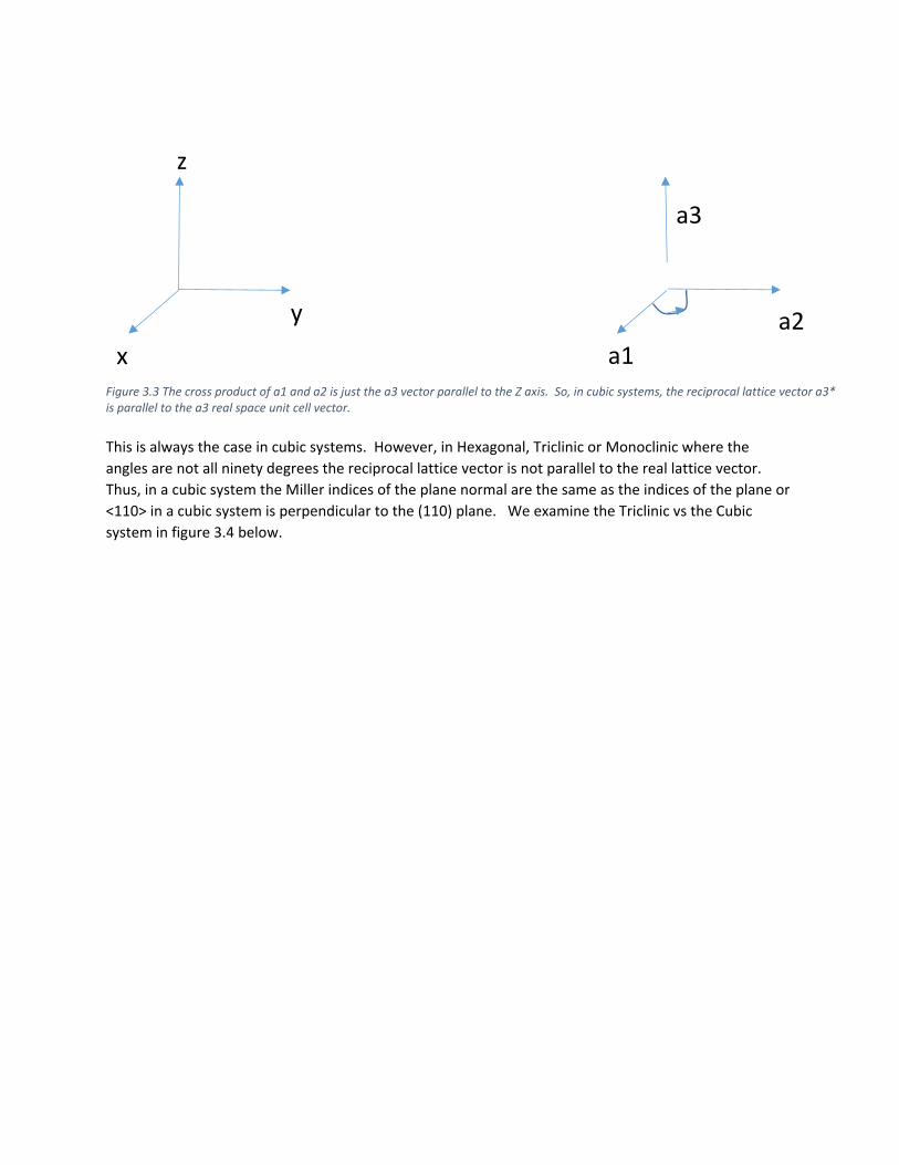
This is always the case in cubic systems. However, in Hexagonal, Triclinic or Monoclinic where the
angles are not all ninety degrees the reciprocal lattice vector is not parallel to the real lattice vector.
Thus, in a cubic system the Miller indices of the plane normal are the same as the indices of the plane or
<110> in a cubic system is perpendicular to the (110) plane. We examine the Triclinic vs the Cubic
system in figure 3.4 below.
x
y
z
a1
a2
a3
Figure 3.3 The cross product of a1 and a2 is just the a3 vector parallel to the Z axis. So, in cubic systems, the reciprocal lattice vector a3* is parallel to the a3 real space unit cell vector.

In Figure 3.3 we speak of the caution we must have in a Triclinic system when we think of Miller indices
and in general we have to take the same caution with plane normals in non-cubic systems as the plane
normal is not simply given by the Miller indices of the plane in the non- cubic system. Similarly,
interplanar distances are much harder to compute for non-cubic systems. Here is the expression for
interplanar spacing in cubic systems:
Dhkl = 𝑎
√ℎ2+𝑘2 𝑙2. Where D is the interplanar spacing and a is the lattice constant, 5.43 Angstrom for
Silicon. And h,k,l are the Miller indices discussed above. We can see right away that our formalism
using the intercept form to describe the plane, of equations 3.1 and 3.2 has resulted in a nice simple
x
y
z
a1
a2
a3 and a3*
Cubic, a1^a2 = a
3.
And so a3* and a
3 are
parallel
x
y
z
a1
1
a2
a3 a
1^a
Triclinic crystal Cubic crystal
a3*
a3
Figure 3.4 Cubic and non-cubic lattices and corresponding reciprocal lattice directions. We must take care as reciprocal lattice vectors in the Triclinic system are not parallel to the regular unit cell directions.
expression. For Silicon, h = k = l = 1, results in the well known spacing observed over and over in TEM,
3.14 Angstrom for the (111) Silicon planes. A number that as a TEM person you will use many times.
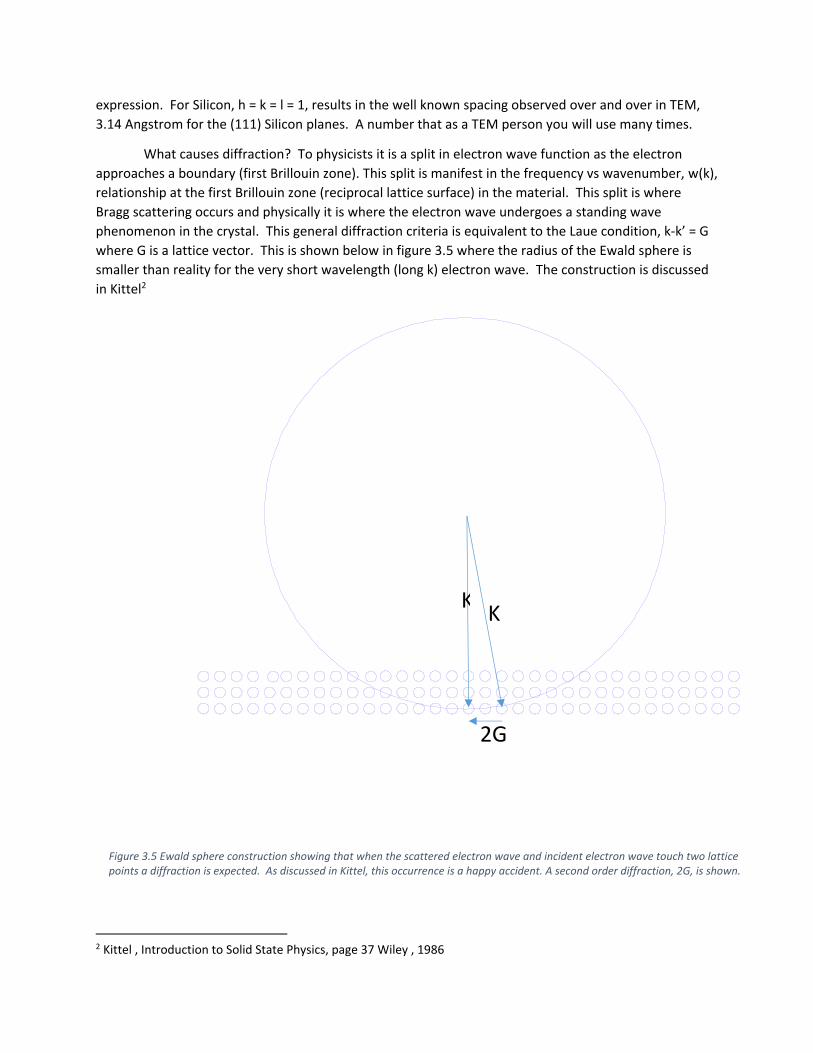
What causes diffraction? To physicists it is a split in electron wave function as the electron
approaches a boundary (first Brillouin zone). This split is manifest in the frequency vs wavenumber, w(k),
relationship at the first Brillouin zone (reciprocal lattice surface) in the material. This split is where
Bragg scattering occurs and physically it is where the electron wave undergoes a standing wave
phenomenon in the crystal. This general diffraction criteria is equivalent to the Laue condition, k-k’ = G
where G is a lattice vector. This is shown below in figure 3.5 where the radius of the Ewald sphere is
smaller than reality for the very short wavelength (long k) electron wave. The construction is discussed
in Kittel2
2 Kittel , Introduction to Solid State Physics, page 37 Wiley , 1986
K’
K
2G
Figure 3.5 Ewald sphere construction showing that when the scattered electron wave and incident electron wave touch two lattice points a diffraction is expected. As discussed in Kittel, this occurrence is a happy accident. A second order diffraction, 2G, is shown.
In Figure 3.5 the points are reciprocal lattice points not real lattice points. The reciprocal lattice
discussed later in the chapter but for now realize that the reciprocal lattice has distances of one over
length and is a more convenient, mathematical construction used in diffraction. The construction of
Figure 3.5 is a three dimensional theorem that holds true in general. We now talk about the two
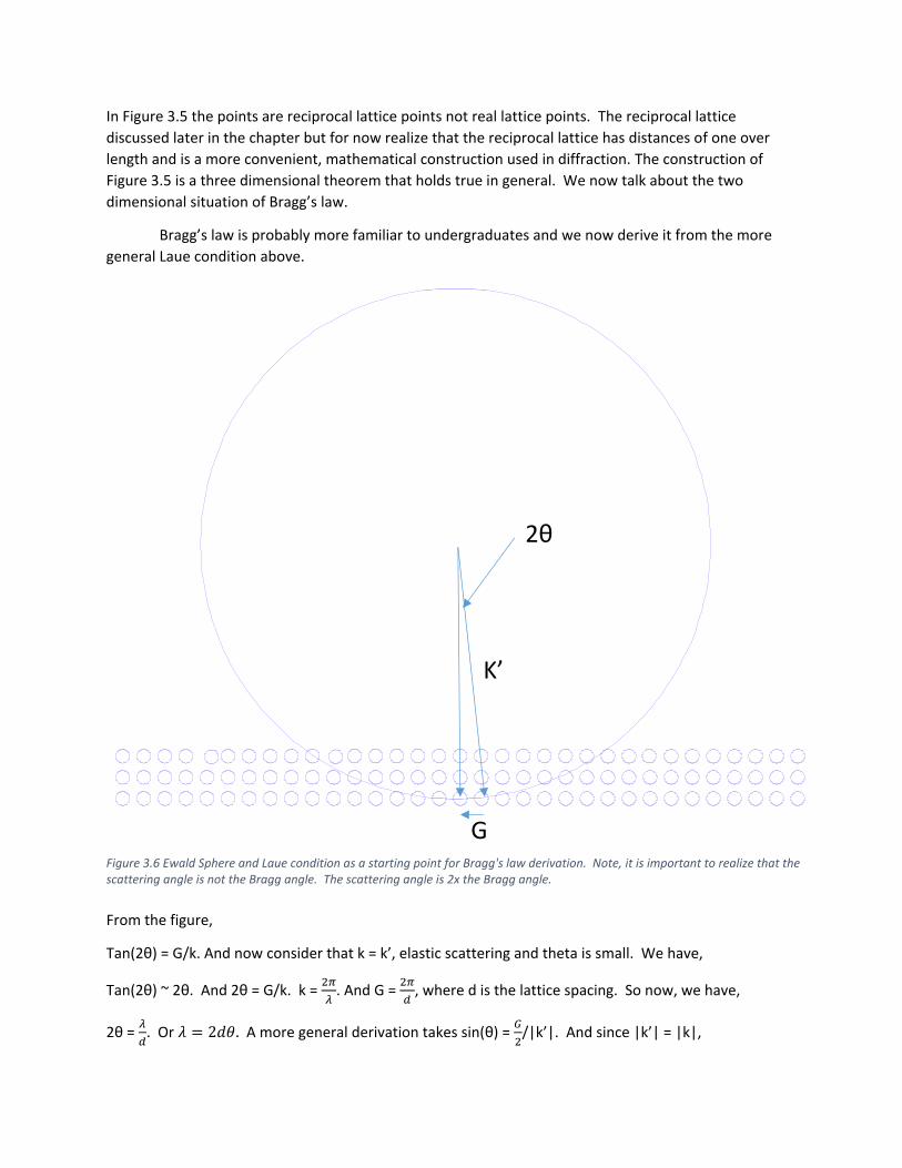
dimensional situation of Bragg’s law.
Bragg’s law is probably more familiar to undergraduates and we now derive it from the more
general Laue condition above.
From the figure,
Tan(2θ) = G/k. And now consider that k = k’, elastic scattering and theta is small. We have,
Tan(2θ) ~ 2θ. And 2θ = G/k. k = 2𝜋
𝜆. And G =
2𝜋
𝑑, where d is the lattice spacing. So now, we have,
2θ = 𝜆
𝑑. Or 𝜆 = 2𝑑𝜃. A more general derivation takes sin(θ) =
𝐺
2/|k’|. And since |k’| = |k|,
K’
G
2θ
Figure 3.6 Ewald Sphere and Laue condition as a starting point for Bragg's law derivation. Note, it is important to realize that the scattering angle is not the Bragg angle. The scattering angle is 2x the Bragg angle.
2Sin(θ) = 𝜆
𝑑. And so,
λ = 2dsinθ. This is the recognizable Bragg’s law for n = 1. A more general derivation takes into account
higher order reflections such as 2G, 3G, 4G, … and this is discussed in Carter and Williams. 3 These
higher order reflections are due to the large diameter of the Ewald Sphere for a TEM. In X-ray
diffraction the Ewald Sphere is much smaller diameter and we are much less likely to see the 2G, 3G
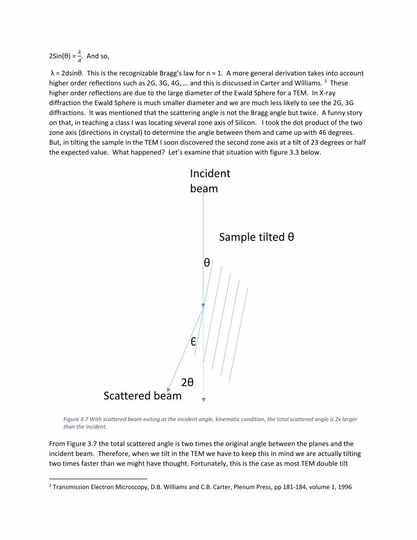
diffractions. It was mentioned that the scattering angle is not the Bragg angle but twice. A funny story
on that, in teaching a class I was locating several zone axis of Silicon. I took the dot product of the two
zone axis (directions in crystal) to determine the angle between them and came up with 46 degrees.
But, in tilting the sample in the TEM I soon discovered the second zone axis at a tilt of 23 degrees or half
the expected value. What happened? Let’s examine that situation with figure 3.3 below.
From Figure 3.7 the total scattered angle is two times the original angle between the planes and the
incident beam. Therefore, when we tilt in the TEM we have to keep this in mind we are actually tilting
two times faster than we might have thought. Fortunately, this is the case as most TEM double tilt
3 Transmission Electron Microscopy, D.B. Williams and C.B. Carter, Plenum Press, pp 181-184, volume 1, 1996
Sample tilted θ
θ
θ
Incident beam
Scattered beam
2θ
Figure 3.7 With scattered beam exiting at the incident angle, kinematic condition, the total scattered angle is 2x larger than the incident.

holders only allow up to 30 degrees of tilt in the Beta direction thus allowing us to access up to 60
degrees separation between zone axes.
Now that we are on the topic of Ewald Spheres lets finish up with discussion of higher order
Laue Zones. In one atom thick TEM sample or ones that are nearly this thin, higher order Laue Zones are
not observed. This dispels the notion that thinner is always better in a TEM sample. For if we have a
thicker sample we can get 3-D information and unit cell dimensions from the first and second order Laue
Zones. Consider figure 3.8 below,
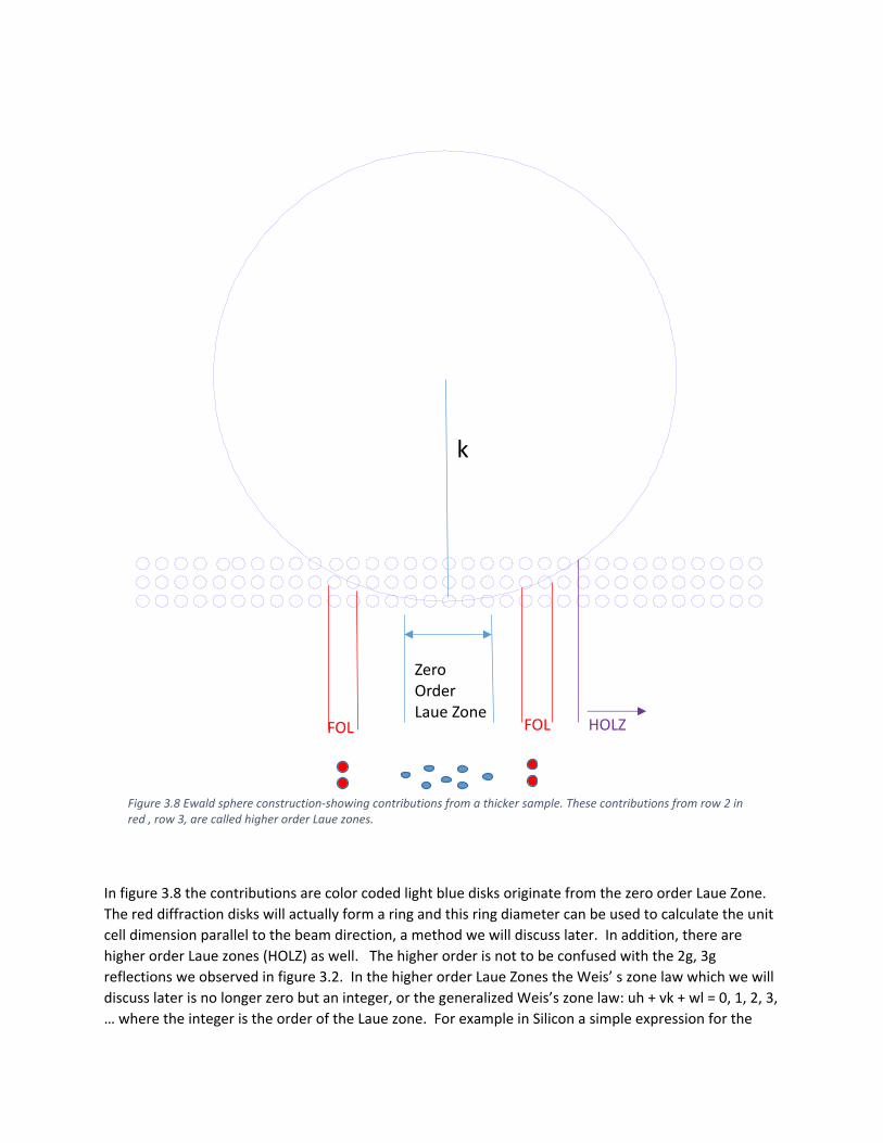
In figure 3.8 the contributions are color coded light blue disks originate from the zero order Laue Zone.
The red diffraction disks will actually form a ring and this ring diameter can be used to calculate the unit
cell dimension parallel to the beam direction, a method we will discuss later. In addition, there are
higher order Laue zones (HOLZ) as well. The higher order is not to be confused with the 2g, 3g
reflections we observed in figure 3.2. In the higher order Laue Zones the Weis’ s zone law which we will
discuss later is no longer zero but an integer, or the generalized Weis’s zone law: uh + vk + wl = 0, 1, 2, 3,
… where the integer is the order of the Laue zone. For example in Silicon a simple expression for the
Zero Order Laue Zone
FOLZ
FOLZ
k
HOLZ
Figure 3.8 Ewald sphere construction-showing contributions from a thicker sample. These contributions from row 2 in red , row 3, are called higher order Laue zones.

<111> zone axis is derived from Weis’s zero order zone law, uh +vk +wl = 0 and since uvw are all 1, we
have
h + k + l = 0 for observed diffraction spots in a Si <111> pattern. If we then have shot our diffraction
pattern with a short camera length and so have captured higher order Laue Zones we would have for
the first order zone diffractions4,
h + k +l = 1. This is a specific case of the <111> zone axis. Let us examine a more physical example of the
Weis’s zone law that may help us tie a few of the concepts together. In figure 3.9 below we see another
example from Silicon but this time the beam comes down the <110> zone axis.
4 Higher order Laue zone effects in electron diffraction and their use in lattice parameter determination, P.M. Jones, G.M. Rackham, J.W. Steeds, Proc. R. Soc. London, A.354 pp 197-222 (1977)
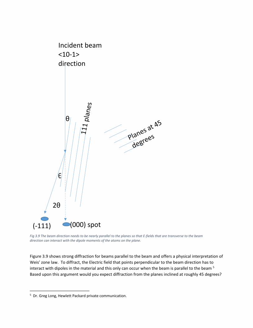
Figure 3.9 shows strong diffraction for beams parallel to the beam and offers a physical interpretation of
Weis’ zone law. To diffract, the Electric field that points perpendicular to the beam direction has to
interact with dipoles in the material and this only can occur when the beam is parallel to the beam 5
Based upon this argument would you expect diffraction from the planes inclined at roughly 45 degrees?
5 Dr. Greg Long, Hewlett Packard private communication.
θ
θ
Incident beam <10-1> direction
2θ
(000) spot (-111)
Fig 3.9 The beam direction needs to be nearly parallel to the planes so that E-fields that are transverse to the beam direction can interact with the dipole moments of the atoms on the plane.

As a hint, consider the planes to be roughly of 110 orientation and consider the Weis’ zone law dot
product.
Notation and brackets around Miller indices. In case you have not figured it out yet, (hkl) refer
to planes, <hkl> is a direction, {hkl} is a family of planes such as {111} area all six planes (111), (111),
(111), (111), (111), and (111). Where boldface is a negative index such as 1 = -1. Similarly <110> is the
family of directions that include [110], [110], [110], [110], [011], [011], [011],[011], [101], [101], [101],
and [101]. A materials scientist is familiar with these 12 slip directions as they are the 12 slip directions
of the close packed plane in an FCC material like Copper or Aluminum.
Let’s use our fundamental’s of reciprocal lattice we have learned so far to create an artificial
diffraction pattern. We will keep it simple and consider the cubic P lattice. The P lattice is short for
primitive and it has a lattice point at all 8 cube vertices as in figure 3.10.
Let us consider the beam coming down the <110> direction of the crystal. From above we know the
Miller indices are reciprocal lattice vectors, this is a cubic situation and so [110] direction of the crystal is
the [110] direction in the reciprocal lattice and so from Weis’s zone law we expect to see only (001),
(110), (111) planes. From our discussion of distance in the reciprocal lattice, we know that low indices
will have the smallest distance from the origin. Thus (110) reflections will be root 2 further from the
origin than the (001) refection. Let’s draw these two reflectors, figure 3.11 below, at 90 degrees to
each other as there dot product is zero.
Figure 3.10 Primitive lattice with an atom at every cube vertices. The eight atom has dotted lines to show that it is hidden and provides perspective.
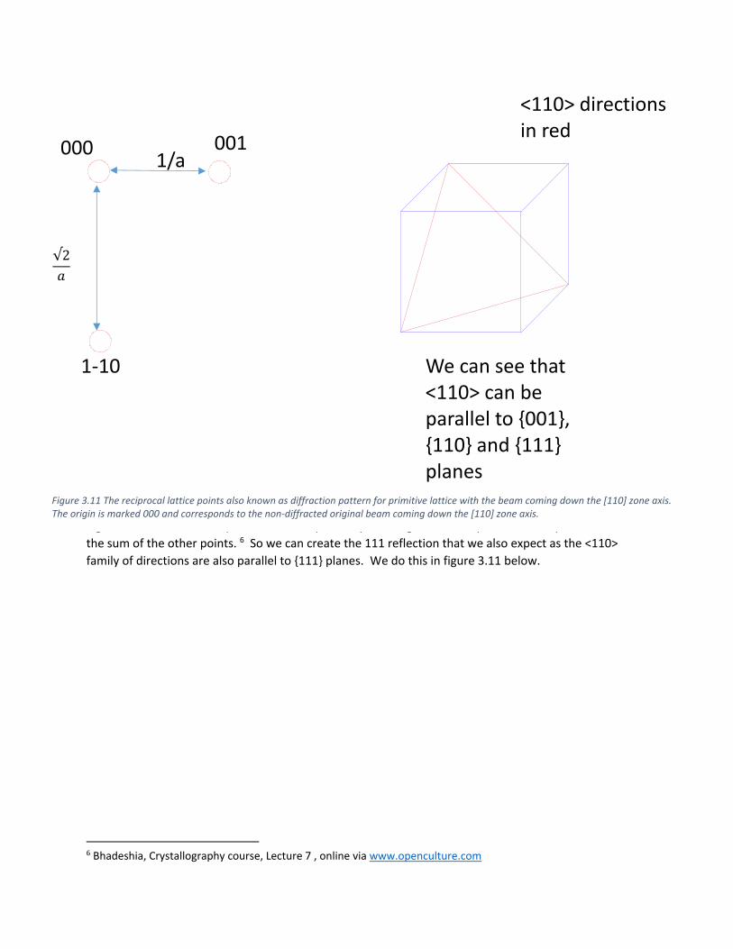
Figure 3.11 can now be expanded to more points by realizing that all the points in a reciprocal lattice are
the sum of the other points. 6 So we can create the 111 reflection that we also expect as the <110>
family of directions are also parallel to {111} planes. We do this in figure 3.11 below.
6 Bhadeshia, Crystallography course, Lecture 7 , online via www.openculture.com
000 001
1-10
<110> directions in red
We can see that <110> can be parallel to {001}, {110} and {111} planes
1/a
√2
𝑎
Figure 3.11 The reciprocal lattice points also known as diffraction pattern for primitive lattice with the beam coming down the [110] zone axis. The origin is marked 000 and corresponds to the non-diffracted original beam coming down the [110] zone axis.
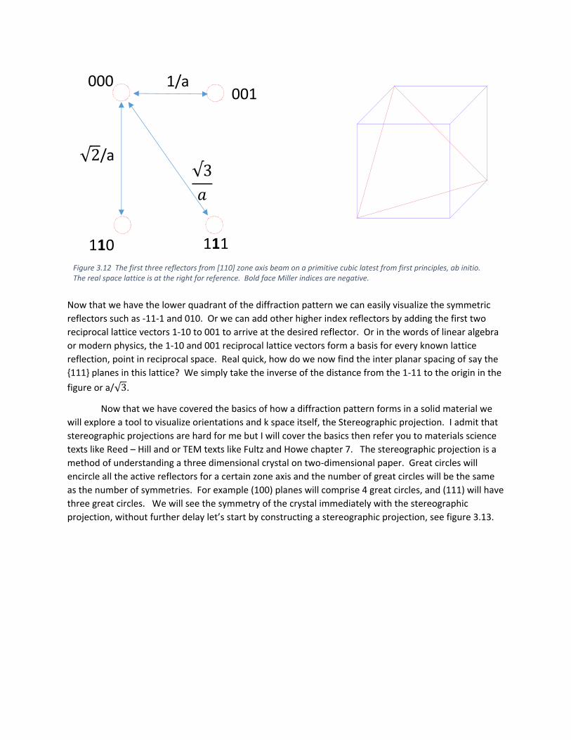
Now that we have the lower quadrant of the diffraction pattern we can easily visualize the symmetric
reflectors such as -11-1 and 010. Or we can add other higher index reflectors by adding the first two
reciprocal lattice vectors 1-10 to 001 to arrive at the desired reflector. Or in the words of linear algebra
or modern physics, the 1-10 and 001 reciprocal lattice vectors form a basis for every known lattice
reflection, point in reciprocal space. Real quick, how do we now find the inter planar spacing of say the
{111} planes in this lattice? We simply take the inverse of the distance from the 1-11 to the origin in the
figure or a/√3.
Now that we have covered the basics of how a diffraction pattern forms in a solid material we
will explore a tool to visualize orientations and k space itself, the Stereographic projection. I admit that
stereographic projections are hard for me but I will cover the basics then refer you to materials science
texts like Reed – Hill and or TEM texts like Fultz and Howe chapter 7. The stereographic projection is a
method of understanding a three dimensional crystal on two-dimensional paper. Great circles will
encircle all the active reflectors for a certain zone axis and the number of great circles will be the same
as the number of symmetries. For example (100) planes will comprise 4 great circles, and (111) will have
three great circles. We will see the symmetry of the crystal immediately with the stereographic
projection, without further delay let’s start by constructing a stereographic projection, see figure 3.13.
√2/a
1/a
√3
𝑎
000
110
001
111
Figure 3.12 The first three reflectors from [110] zone axis beam on a primitive cubic latest from first principles, ab initio. The real space lattice is at the right for reference. Bold face Miller indices are negative.
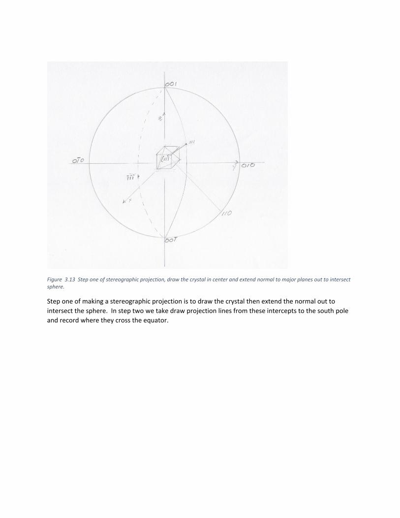
Figure 3.13 Step one of stereographic projection, draw the crystal in center and extend normal to major planes out to intersect sphere.
Step one of making a stereographic projection is to draw the crystal then extend the normal out to
intersect the sphere. In step two we take draw projection lines from these intercepts to the south pole
and record where they cross the equator.

Figure 3.14 Step 2 of a stereographic projection from two planes as drawn, 110 plane and 111 plane. The normal to these two planes intersect the sphere. A projection of these planes to South Pole is done with dotted line and x marks where that projection crosses equatorial plane.
The two planes of the crystal in figure 3.14 give the two x spots. One on the equator edge at 110 and
the other towards upper right at 111. Now we draw the equatorial plane to show these intersections
more clearly, figure 3.15 below.
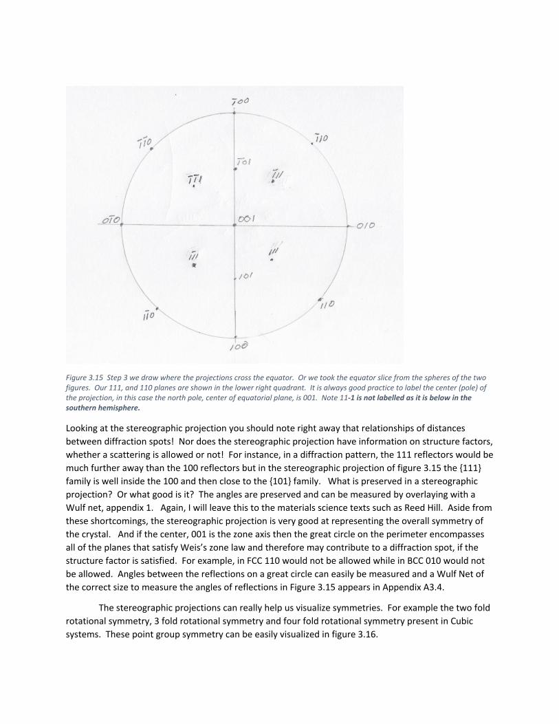
Figure 3.15 Step 3 we draw where the projections cross the equator. Or we took the equator slice from the spheres of the two figures. Our 111, and 110 planes are shown in the lower right quadrant. It is always good practice to label the center (pole) of the projection, in this case the north pole, center of equatorial plane, is 001. Note 11-1 is not labelled as it is below in the southern hemisphere.
Looking at the stereographic projection you should note right away that relationships of distances
between diffraction spots! Nor does the stereographic projection have information on structure factors,
whether a scattering is allowed or not! For instance, in a diffraction pattern, the 111 reflectors would be
much further away than the 100 reflectors but in the stereographic projection of figure 3.15 the {111}
family is well inside the 100 and then close to the {101} family. What is preserved in a stereographic
projection? Or what good is it? The angles are preserved and can be measured by overlaying with a
Wulf net, appendix 1. Again, I will leave this to the materials science texts such as Reed Hill. Aside from
these shortcomings, the stereographic projection is very good at representing the overall symmetry of
the crystal. And if the center, 001 is the zone axis then the great circle on the perimeter encompasses
all of the planes that satisfy Weis’s zone law and therefore may contribute to a diffraction spot, if the
structure factor is satisfied. For example, in FCC 110 would not be allowed while in BCC 010 would not
be allowed. Angles between the reflections on a great circle can easily be measured and a Wulf Net of
the correct size to measure the angles of reflections in Figure 3.15 appears in Appendix A3.4.
The stereographic projections can really help us visualize symmetries. For example the two fold
rotational symmetry, 3 fold rotational symmetry and four fold rotational symmetry present in Cubic
systems. These point group symmetry can be easily visualized in figure 3.16.
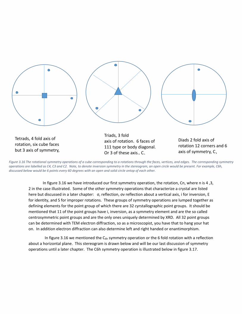
In figure 3.16 we have introduced our first symmetry operation, the rotation, Cn, where n is 4 ,3,
2 in the case illustrated. Some of the other symmetry operations that characterize a crystal are listed
here but discussed in a later chapter: σ, reflection, σv reflection about a vertical axis, i for inversion, E
for identity, and S for improper rotations. These groups of symmetry operations are lumped together as
defining elements for the point group of which there are 32 cyrstallographic point groups. It should be
mentioned that 11 of the point groups have i, inversion, as a symmetry element and are the so called
centrosymmetric point groups and are the only ones uniquely determined by XRD. All 32 point groups
can be determined with TEM electron diffraction, so as a microscopist, you have that to hang your hat
on. In addition electron diffraction can also determine left and right handed or enantimorphism.
In figure 3.16 we mentioned the C6h symmetry operation or the 6 fold rotation with a reflection
about a horizontal plane. This stereogram is drawn below and will be our last discussion of symmetry
operations until a later chapter. The C6h symmetry operation is illustrated below in figure 3.17.
Tetrads, 4 fold axis of rotation, six cube faces but 3 axis of symmetry, C
Diads 2 fold axis of rotation 12 corners and 6 axis of symmetry, C
2
Triads, 3 fold axis of rotation. 6 faces of 111 type or body diagonal. Or 3 of these axis., C
3
Figure 3.16 The rotational symmetry operations of a cube corresponding to a rotations through the faces, vertices, and edges. The corresponding symmetry operations are labelled as C4, C3 and C2. Note, to denote inversion symmetry in the stereogram, an open circle would be present. For example, C6h, discussed below would be 6 points every 60 degrees with an open and solid circle ontop of each other.
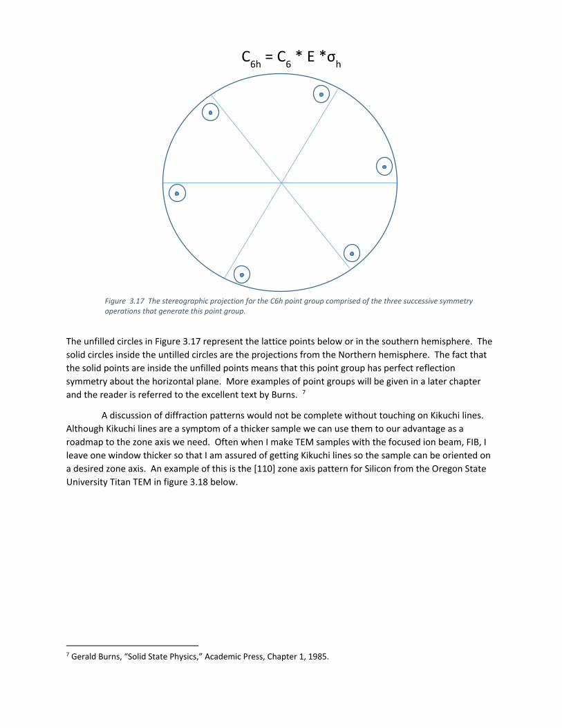
The unfilled circles in Figure 3.17 represent the lattice points below or in the southern hemisphere. The
solid circles inside the untilled circles are the projections from the Northern hemisphere. The fact that
the solid points are inside the unfilled points means that this point group has perfect reflection
symmetry about the horizontal plane. More examples of point groups will be given in a later chapter
and the reader is referred to the excellent text by Burns. 7
A discussion of diffraction patterns would not be complete without touching on Kikuchi lines.
Although Kikuchi lines are a symptom of a thicker sample we can use them to our advantage as a
roadmap to the zone axis we need. Often when I make TEM samples with the focused ion beam, FIB, I
leave one window thicker so that I am assured of getting Kikuchi lines so the sample can be oriented on
a desired zone axis. An example of this is the [110] zone axis pattern for Silicon from the Oregon State
University Titan TEM in figure 3.18 below.
7 Gerald Burns, “Solid State Physics,” Academic Press, Chapter 1, 1985.
C6h
= C6 * E *σ
h
Figure 3.17 The stereographic projection for the C6h point group comprised of the three successive symmetry operations that generate this point group.

Laue Zone, the ring with red arrow.
Freidels law.
Point group
Space group
CBED vs SAED
The slightly offcenter pattern, due to not being able to re do it during Covid 19 shutdown shows the
Kikuchi bands and the first order Laue Zone. The Kikuchi lines intersect at a zone axis, in this case the
[110] zone axis. As we tilt the beam we look for the intersection of the Kikuchi lines to go towards the
middle of the screen. We use alpha tilt to move the intersection (zone axis right and left) and beta tilt to
move the zone axis up and down. Obviously, we needed to move this zone axis a bit more to the right
with slightly more alpha tilt. Just as a note, the radius of the first Holz (Higher order Laue Zone) can be
used to calculate the unit cell dimensions perpendicular to the beam. A more expanded pattern, larger
camera length is then used to calculate the dimensions of lattice constant parallel to the beam using the
zero order Laue zone spots.
We present a short discussion on how to draw your own Kikuchi bands given an indexed
diffraction pattern. Using one of the indexed patterns in Williams and Carter or Fultz and Howe we
draw a line from the pattern center to reflector hkl. Then we draw a perpendicular bisector to this line
Figure 3.18 Si in rough 110 orientation and corresponding cross of Kikuchi lines in blue. Also seen on the right side is the First order Laue Zone ring marked in red arrows.
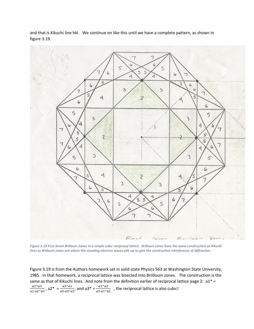
and that is Kikuchi line hkl. We continue on like this until we have a complete pattern, as shown in
figure 3.19.
Figure 3.19 Frist Seven Brillouin Zones in a simple cubic reciprocal lattice. Brillouin zones have the same construction as Kikuchi lines as Brillouin zones are where the standing electron waves pile up to give the constructive interference of diffraction.
Figure 3.19 is from the Authors homework set in solid state Physics 563 at Washington State University,
1985. In that homework, a reciprocal lattice was bisected into Briillouin zones. The construction is the
same as that of Kikuchi lines. And note from the definition earlier of reciprocal lattice page 2: a1* = 𝑎2^𝑎3
𝑎1∙𝑎2^𝑎3 , a2* =
𝑎3^𝑎1
𝑎2∙𝑎3^𝑎1, and a3* =
𝑎1^𝑎2
𝑎3∙𝑎1^𝑎2 , the reciprocal lattice is also cubic!

Actual TEM samples have a disk shape to them and the disk has a thickness, so the Ewald sphere
constructions of earlier figures in this chapter need to be modified for real world samples. The idealized
lattice needs to be convolved with the FT of the sample disk. The resultant are “relrods” or ellipses in
reciprocal lattice space as follows in figure 3.20.
So, now, the diffraction becomes easier to obtain. This elongation is one aspect of electron diffraction
that is a plus and a minus. On the plus side, it does allow for more planes to satisfy the diffraction
Lattice
FT of Lattice
Sample
FT of sample
⊛ =
Actual reciprocal lattice
Figure 3.20 The effect of sample shape on reciprocal lattice. The former points of reciprocal lattice become relrods.
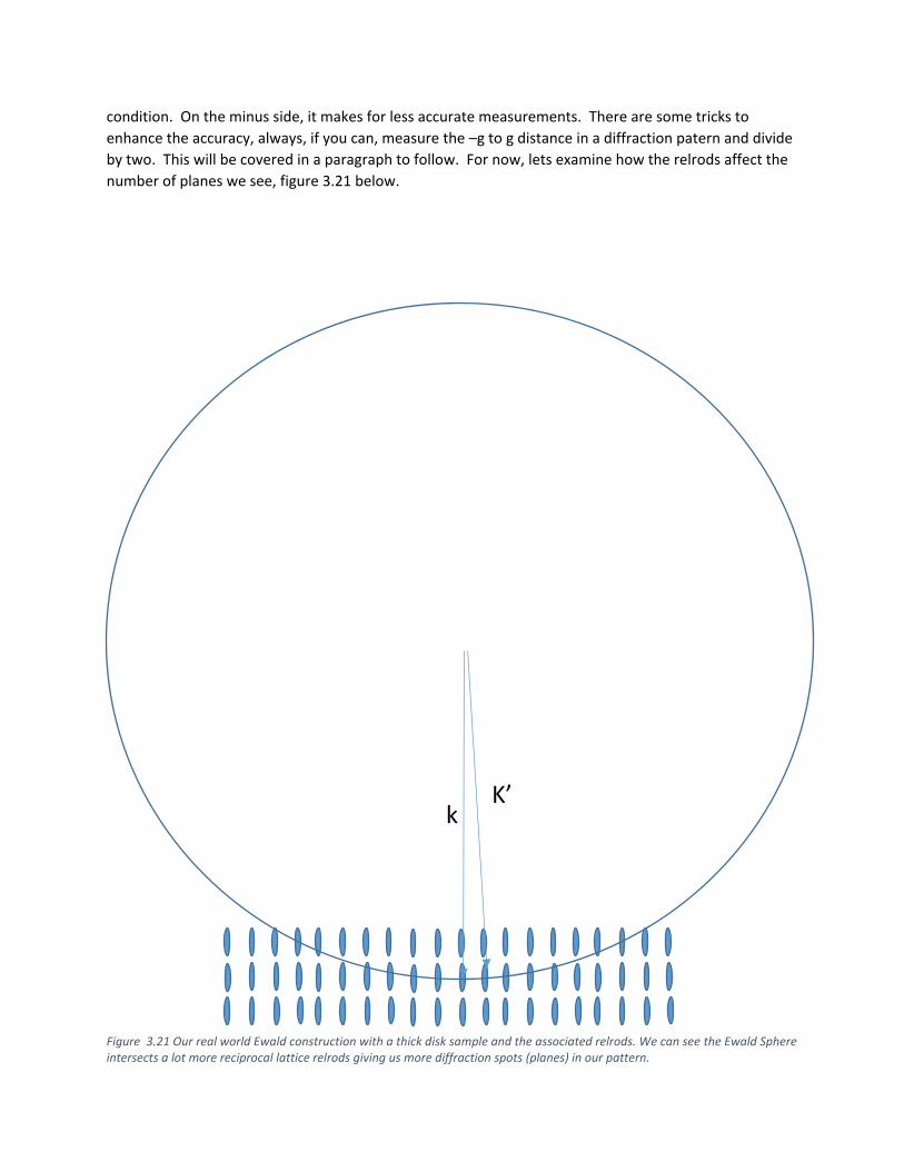
condition. On the minus side, it makes for less accurate measurements. There are some tricks to
enhance the accuracy, always, if you can, measure the –g to g distance in a diffraction patern and divide
by two. This will be covered in a paragraph to follow. For now, lets examine how the relrods affect the
number of planes we see, figure 3.21 below.
k
K’
Figure 3.21 Our real world Ewald construction with a thick disk sample and the associated relrods. We can see the Ewald Sphere intersects a lot more reciprocal lattice relrods giving us more diffraction spots (planes) in our pattern.
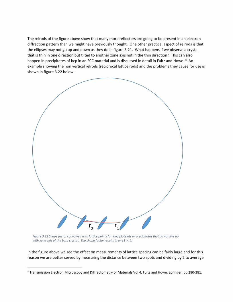
The relrods of the figure above show that many more reflectors are going to be present in an electron
diffraction pattern than we might have previously thought. One other practical aspect of relrods is that
the ellipses may not go up and down as they do in figure 3.21. What happens if we observe a crystal
that is thin in one direction but tilted to another zone axis not in the thin direction? This can also
happen in precipitates of hcp in an FCC material and is discussed in detail in Fultz and Howe. 8 An
example showing the non vertical relrods (reciprocal lattice rods) and the problems they cause for use is
shown in figure 3.22 below.
In the figure above we see the effect on measurements of lattice spacing can be fairly large and for this
reason we are better served by measuring the distance between two spots and dividing by 2 to average
8 Transmission Electron Microscopy and Diffractometry of Materials Vol 4, Fultz and Howe, Springer, pp 280-281.
r1 r
2
Figure 3.22 Shape factor convolved with lattice points for long platelets or precipitates that do not line up with zone axis of the base crystal. The shape factor results in an r1 > r2.
out shape factor distortion like this. Diffraction Tools, a freeware plugin for the Digital Micrograph
software has a provision for center to point measurement or the preferred point-to-point measurement
(where it takes care of dividing by two and inverting the reciprocal lattice distance to real distance in
nanometers. Examples using Digital Micrograph are presented in the Appendix.
Complex patterns around bright central spots are sometimes seen in alloys or multiphase
materials. Some of these shapes are due to the case of “superlattice” reflections – breaking of excluded
reflectors by chemical substitution in the lattice and others are due to a secondary phase. We will now
discuss both of these. The terminology of “superlattice” is not familiar to all of the materials scientists
that I have encountered. For years I was calling attention to some weak reflectors in a student’s sample
and saying they were evidence of a super lattice. This assistant professor kept sending the student back
to look for a “secondary phase.” Finally, I realized that what the assistant professor was calling a
secondary phase was actually the “superlattice” reflections that we had observed long ago. Or we were
talking about the same phenomenon but using a different language.
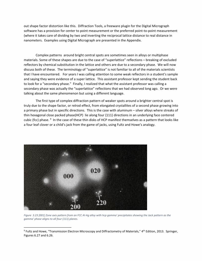
The first type of complex diffraction pattern of weaker spots around a brighter central spot is
truly due to the shape factor, or relrod effect, from elongated crystallites of a second phase growing into
a primary phase but in specific directions. This is the case with aluminum – silver alloys where streaks of
thin hexagonal close packed phase(HCP) lie along four {111} directions in an underlying face centered
cubic (fcc) phase. 9 In the case of these thin disks of HCP manifest themselves as a pattern that looks like
a four leaf clover or a child’s jack from the game of jacks, using Fultz and Howe’s analogy.
Figure 3.23 [001] Zone axis pattern from an FCC Al-Ag alloy with hcp gamma' precipitates showing the Jack pattern as the gamma' phase aligns to all four (111) planes.
9 Fultz and Howe, “Transmission Electron Microscopy and Diffractometry of Materials,” 4th Edition, 2013. Springer, Figures 6.27 and 6.26.
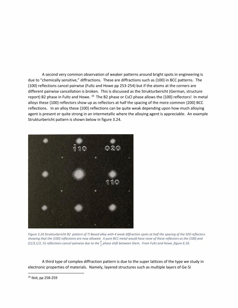
A second very common observation of weaker patterns around bright spots in engineering is
due to “chemically sensitive,” diffractions. These are diffractions such as {100} in BCC patterns. The
(100) reflections cancel pairwise (Fultz and Howe pp 253-254) but if the atoms at the corners are
different pairwise cancellation is broken. This is discussed as the Strukturbericht (German, structure
report) B2 phase in Fultz and Howe. 10 The B2 phase or CsCl phase allows the {100} reflectors! In metal
alloys these {100} reflectors show up as reflectors at half the spacing of the more common {200} BCC
reflections. In an alloy these {100} reflections can be quite weak depending upon how much alloying
agent is present or quite strong in an intermetallic where the alloying agent is appreciable. An example
Strukturbericht pattern is shown below in figure 3.24.
Figure 3.24 Strukturbericht B2 pattern of Ti Based alloy with 4 weak diffraction spots at half the spacing of the 020 reflectors showing that the {100} reflections are now allowed. A pure BCC metal would have none of these reflectors as the (100) and
((1/2,1/2, ½) reflections cancel pairwise due to the 𝜋
2 phase shift between them. From Fultz and Howe, figure 6.10.
A third type of complex diffraction pattern is due to the super lattices of the type we study in
electronic properties of materials. Namely, layered structures such as multiple layers of Ge-Si
10 Ibid, pp 258-259

heterojunction solar cells, GaAs – AlGaAs light emitting diode structures. If the layers are thin and
periodic we will see fine points that blur the diffraction pattern in the direction of the layers.
A fourth very advanced pattern is double diffraction from two phases. In double diffraction,
there are second set of reflectors that have lattice constants that differ by the difference of the two
lattice constants and these patterns can be very difficult to interpret. I am looking for examples of
double diffraction, so if you have one please let me know and will happily add it to this discussion.
Double diffraction can be a real test of your geometry skills.
Diffraction relies heavily on our ability to visualize geometrical patterns. To help with that we
have discussed plane geometry, the Miller Indices, the Ewald sphere construction as an alternative to
Bragg’s diffraction law, remember k – k’ = g? The stereographic projection was also introduced as a way
to visualize and measure angles in a diffraction pattern, although to be honest I simply form the dot
product between to zone axis that I want and compute the angle directly. However, for some the
stereographic projection is helpful. If your struggle with it, as I do, you can be a diffraction success
without it. Relrods or shape factors from the convolution of sample shape and diffraction relax
diffraction conditions. Finally, more advanced diffraction phenomenon like secondary phases,
superlattice or Strukturbericht patterns were introduced. Diffraction is a whole discipline to itself and
every day I learn something new, keep an open mind and keep learning.
Appendix, Indexing patterns.
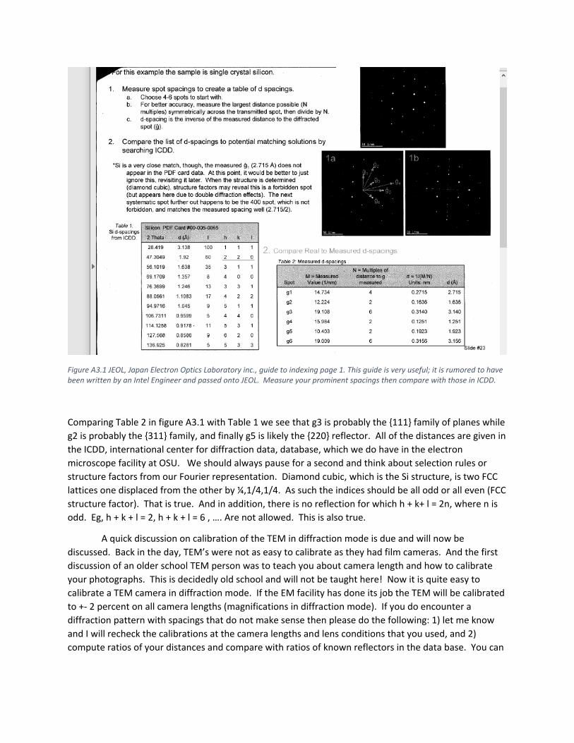
Figure A3.1 JEOL, Japan Electron Optics Laboratory inc., guide to indexing page 1. This guide is very useful; it is rumored to have been written by an Intel Engineer and passed onto JEOL. Measure your prominent spacings then compare with those in ICDD.
Comparing Table 2 in figure A3.1 with Table 1 we see that g3 is probably the {111} family of planes while
g2 is probably the {311} family, and finally g5 is likely the {220} reflector. All of the distances are given in
the ICDD, international center for diffraction data, database, which we do have in the electron
microscope facility at OSU. We should always pause for a second and think about selection rules or
structure factors from our Fourier representation. Diamond cubic, which is the Si structure, is two FCC
lattices one displaced from the other by ¼,1/4,1/4. As such the indices should be all odd or all even (FCC
structure factor). That is true. And in addition, there is no reflection for which h + k+ l = 2n, where n is
odd. Eg, h + k + l = 2, h + k + l = 6 , …. Are not allowed. This is also true.
A quick discussion on calibration of the TEM in diffraction mode is due and will now be
discussed. Back in the day, TEM’s were not as easy to calibrate as they had film cameras. And the first
discussion of an older school TEM person was to teach you about camera length and how to calibrate
your photographs. This is decidedly old school and will not be taught here! Now it is quite easy to
calibrate a TEM camera in diffraction mode. If the EM facility has done its job the TEM will be calibrated
to +- 2 percent on all camera lengths (magnifications in diffraction mode). If you do encounter a
diffraction pattern with spacings that do not make sense then please do the following: 1) let me know
and I will recheck the calibrations at the camera lengths and lens conditions that you used, and 2)
compute ratios of your distances and compare with ratios of known reflectors in the data base. You can
often index an un-calibrated TEM in this manner as the ratio of distances cancels out the unknown
camera length (magnification factor).
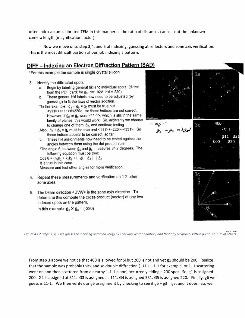
Now we move onto step 3,4, and 5 of indexing, guessing at reflectors and zone axis verification.
This is the most difficult portion of our job indexing a pattern.
From step 3 above we notice that 400 is allowed for Si but 200 is not and yet g1 should be 200. Realize
that the sample was probably thick and so double diffraction (111 +1-1-1 for example, or 111 scattering
went on and then scattered from a nearby 1-1-1 plane) occurred yielding a 200 spot. So, g1 is assigned
200. G2 is assigned at 311. G3 is assigned as 111. G4 is assigned 331. G5 is assigned 220. Finally, g6 we
guess is 11-1. We then verify our g6 assignment by checking to see if g6 + g3 = g5, and it does. So, we
Figure A3.2 Steps 3, 4, 5 we guess the indexing and then verify by checking vector addition, and that any reciprocal lattice point is a sum of others.
guessed correctly on g6. Now let’s try other additions, from inspection of the above we should have g3
+ g1 = g2,
and g3 + g1 = 111 +200 = 311 that is our guess for g2. So, far so good. Let’s finally check the last
triangle of vectors, g3 + g5 = g4? Remember we add vectors head to tail so g3 slides over to the tail of
g5 make the last leg of triangle. And checking this vector addition,
g3 + g5 = 111 + 220 = 331. Since g4 does equal 331. We have the final check, g3 + g5 = g4. We are done
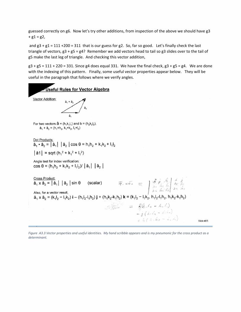
with the indexing of this pattern. Finally, some useful vector properties appear below. They will be
useful in the paragraph that follows where we verify angles.
Figure A3.3 Vector properties and useful identities. My hand scribble appears and is my pneumonic for the cross product as a determinant.

We will do a more difficult example next using a student sample. In this case the student, from
U of Oregon, came to OSU for indexing some samples that were Titanium dioxide. But there are two
phases of Titanium dioxide, Anatase and Rutile. So, which one did she have? After collecting the
patterns we set about to characterize them and those thoughts are presented here.
Figure A3.4 The near zone axis pattern for a crystallite of a mineral thought to be a phase of Titania. Marissa Acosta, University of Oregon. The distances, nm, were measured using the free “Digital micrograph: plug-in called Diffraction tools.
Next we write down all of the distances and how many there were and compare with distances
from the International Center for Diffraction Data base (ICDD).

Figure A3.5 The diffraction peaks were jotted down along with the number of them. Anatase distances did not match observed.
Once the diffraction peaks were determined, we started comparing the distances from the
known distances found in JEMS or the ICDD software. Note, that there are errors in the JEMS database
and to save embarrassment, I would stick with the ICDD. However, later, JEMS can be used and was
used to simulate the pattern as the JEMS simulation tools are superior. Rutile <113> was selected as a
candidate and now have to go through and reconcile that with Figure A3.6 below from the ICDD
database.
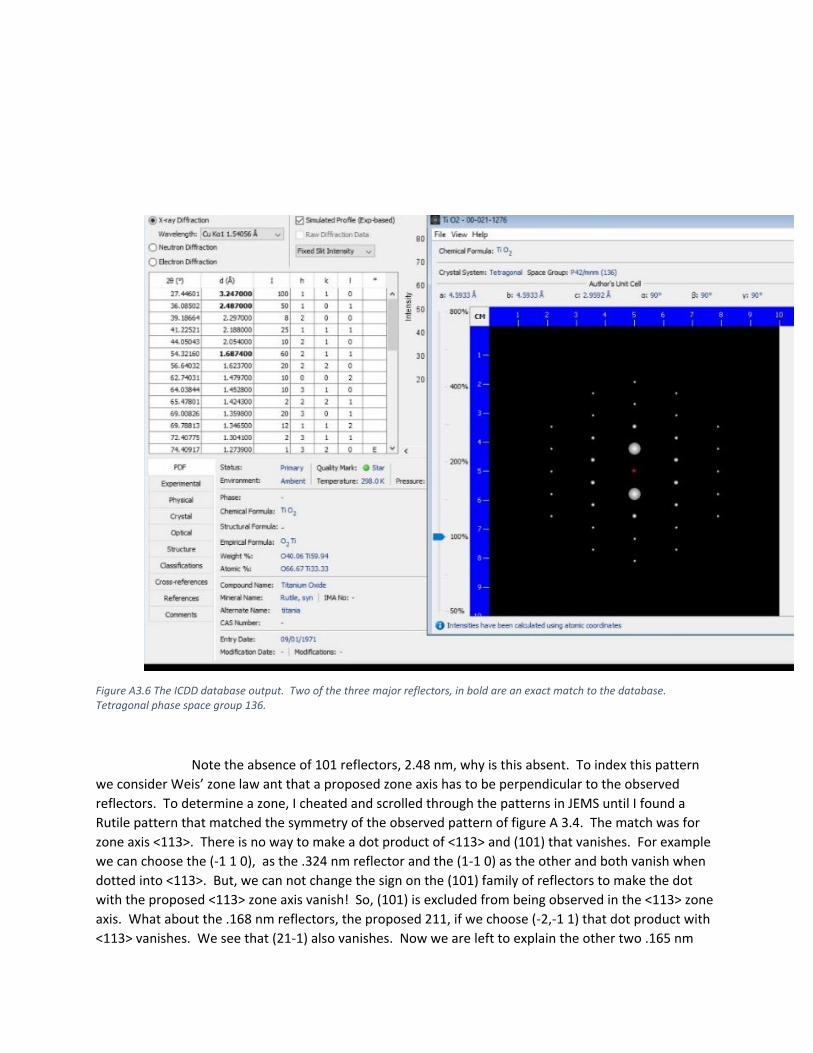
Figure A3.6 The ICDD database output. Two of the three major reflectors, in bold are an exact match to the database. Tetragonal phase space group 136.
Note the absence of 101 reflectors, 2.48 nm, why is this absent. To index this pattern
we consider Weis’ zone law ant that a proposed zone axis has to be perpendicular to the observed
reflectors. To determine a zone, I cheated and scrolled through the patterns in JEMS until I found a
Rutile pattern that matched the symmetry of the observed pattern of figure A 3.4. The match was for
zone axis <113>. There is no way to make a dot product of <113> and (101) that vanishes. For example
we can choose the (-1 1 0), as the .324 nm reflector and the (1-1 0) as the other and both vanish when
dotted into <113>. But, we can not change the sign on the (101) family of reflectors to make the dot
with the proposed <113> zone axis vanish! So, (101) is excluded from being observed in the <113> zone
axis. What about the .168 nm reflectors, the proposed 211, if we choose (-2,-1 1) that dot product with
<113> vanishes. We see that (21-1) also vanishes. Now we are left to explain the other two .165 nm
reflectors and find those by realizing that in the tetragonal system we can permute the h, k as those
have the same distance. Therefore, the other two reflectors are (1 2-1) and (-1-2 1). Now we have all
four .168 nm reflectors that vanish when dotted into <113>. We are confident but now further check
by looking further down the list, we also see four .136 nm reflectors we observed quite readily in the
pattern. Those are the (0 3-1), (-301), (30-1), and (0 3-1). We notice all four of these vanish when
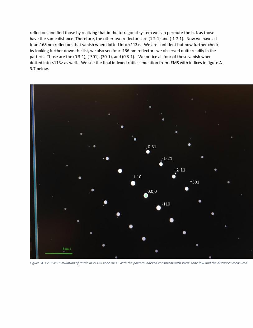
dotted into <113> as well. We see the final indexed rutile simulation from JEMS with indices in figure A
3.7 below.
-1-21
-2-11
0-31
-301 1-10
0,0,0
-110
Figure A 3.7 JEMS simulation of Rutile in <113> zone axis. With the pattern indexed consistent with Weis' zone law and the distances measured
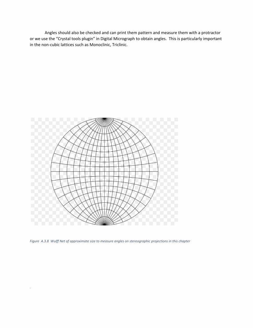
Angles should also be checked and can print them pattern and measure them with a protractor
or we use the “Crystal tools plugin” in Digital Micrograph to obtain angles. This is particularly important
in the non-cubic lattices such as Monoclinic, Triclinic.
Figure A.3.8 Wulff Net of approximate size to measure angles on stereographic projections in this chapter
.
-1-21
0-31
-301
1-10