Embed Size (px)
Citation preview

16
CHAPTER 3
DEVELOPMENT METHODOLOGY
3.1.1 Design Specification
This project is mainly about using IR transmission to transmit signal derived from
the computer peripheral. There are a few considerations that is to be made in this
project, to determine the viability of the transmission. The length of the
transmission is approximate around 0.194 -0.235 m for the IR transmission from
the mouse or the keyboard. Any length beyond the limits requires source link
alignment to maximize energy received It is much less than the projected length
of 100cm-150cm.
The infrared printer ideally is to be designed to operate within the length of
200cm-300cm. Due unavailability of the photodiode TD6061 needed to build the
infrared link to the printer. Whereas the printer needs a decoder to decode the
received signal. The project shall be made to be a success by solving both the
problems.
17
3.2.1 Infrared Wireless Mouse (Internal Structure)
The internal structure of the infrared mouse is divided into 2 sections. The first
section is govern by the MA6221-Q17K IC manufactured by Agilent, which
control the infrared transmission of the device and link the communication of the
mouse to the center processing unit. The Section is governed by the ADNS-2000
IC which controls the optical sensor of the mouse. Both of these devices have a
supporting oscillator input which is synchronized using a crystal input.
3.2.2 The MA6221-Q17K IC
The MA6221-Q17K IC is an encoder IC that can encode data from the mouse
optical sensor and send it via RF, Blue Tooth, Infrared etc. The IC is equipped
with a complete set of FSK modulator which is possible for any wireless
transmission. There are 2 kinds of output from the optical mouse sensor; they are
the quadrature and SPI (serial peripheral interface) which is being supported
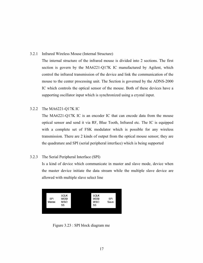
3.2.3 The Serial Peripheral Interface (SPI)
Is a kind of device which communicate in master and slave mode, device when
the master device initiate the data stream while the multiple slave device are
allowed with multiple slave select line
Figure 3.23 : SPI block diagram me
18
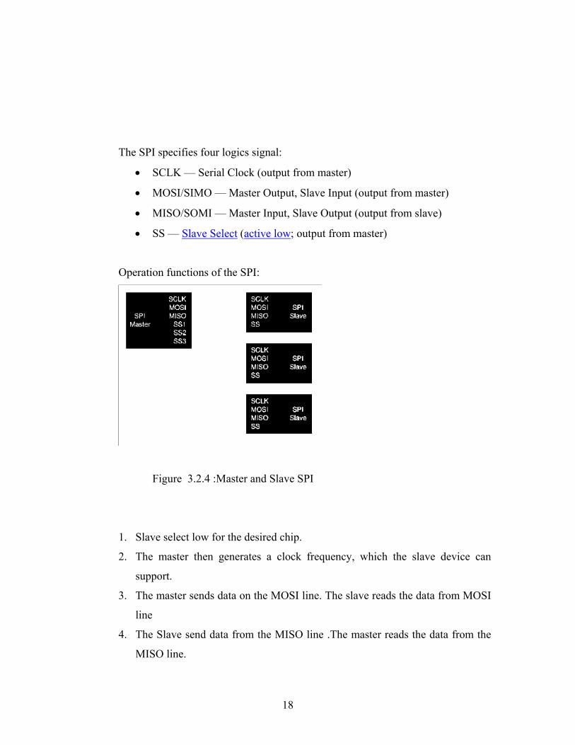
The SPI specifies four logics signal:
• SCLK — Serial Clock (output from master)
• MOSI/SIMO — Master Output, Slave Input (output from master)
• MISO/SOMI — Master Input, Slave Output (output from slave)
• SS — Slave Select (active low; output from master)
Operation functions of the SPI:
Figure 3.2.4 :Master and Slave SPI
1. Slave select low for the desired chip.
2. The master then generates a clock frequency, which the slave device can
support.
3. The master sends data on the MOSI line. The slave reads the data from MOSI
line
4. The Slave send data from the MISO line .The master reads the data from the
MISO line.
19
3.2.4 Features of the MA6221-Q17K IC
• 76.8KHz clock rate
• Hi speed & 32.76 KHz OSC supported.
• Build in data scrambler and error detection encoder.
• Build in single dual signal generator ,modulator and amplifier
• 3V/5V DC embedded.
• X/Y axis supported for both quadrate and SPI input.
• Z axis supports for optical mouse and mechanical inputs.
3.2.5 Device Connection for the Infrared Mouse:
The connection of the MA6221_Q17K IC to the mouse operation controller is
based on the IC ADNS-2000 .These IC will decode all the instruction executed by
the mouse and transmit these instruction in binary. Pin such as Y2IN, Y1IN, XIN,
X2IN,Z2IN,Z1IN are all the function control by the IC ADNS-2000.All these pin
represent the three dimensional area x,y,z which is determined by the sensor of
the mouse ,when it sense an object. Whereas the infrared wireless transmission
part is totally control by the MA6221_Q17K IC
20
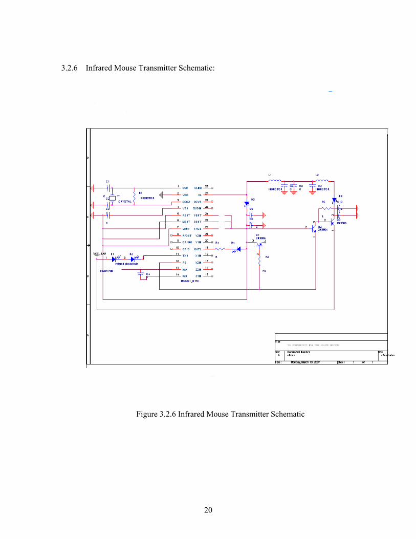
3.2.6 Infrared Mouse Transmitter Schematic:
Figure 3.2.6 Infrared Mouse Transmitter Schematic
21
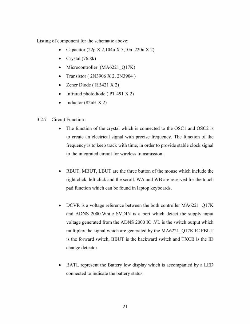
Listing of component for the schematic above:
• Capacitor (22p X 2,104u X 5,10n ,220u X 2)
• Crystal (76.8k)
• Microcontroller (MA6221_Q17K)
• Transistor ( 2N3906 X 2, 2N3904 )
• Zener Diode ( RB421 X 2)
• Infrared photodiode ( PT 491 X 2)
• Inductor (82uH X 2)
3.2.7 Circuit Function :
• The function of the crystal which is connected to the OSC1 and OSC2 is
to create an electrical signal with precise frequency. The function of the
frequency is to keep track with time, in order to provide stable clock signal
to the integrated circuit for wireless transmission.
• RBUT, MBUT, LBUT are the three button of the mouse which include the
right click, left click and the scroll. WA and WB are reserved for the touch
pad function which can be found in laptop keyboards.
• DCVR is a voltage reference between the both controller MA6221_Q17K
and ADNS 2000.While SVDIN is a port which detect the supply input
voltage generated from the ADNS 2000 IC .VL is the switch output which
multiplex the signal which are generated by the MA6221_Q17K IC.FBUT
is the forward switch, BBUT is the backward switch and TXCB is the ID
change detector.
• BATL represent the Battery low display which is accompanied by a LED
connected to indicate the battery status.
22
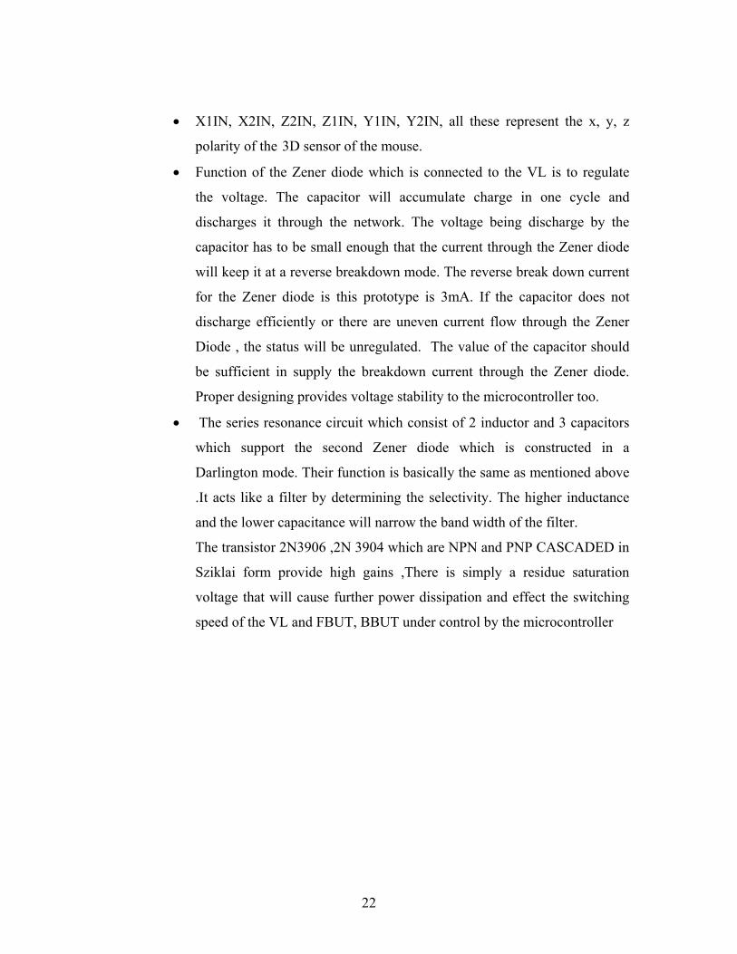
• X1IN, X2IN, Z2IN, Z1IN, Y1IN, Y2IN, all these represent the x, y, z
polarity of the 3D sensor of the mouse.
• Function of the Zener diode which is connected to the VL is to regulate
the voltage. The capacitor will accumulate charge in one cycle and
discharges it through the network. The voltage being discharge by the
capacitor has to be small enough that the current through the Zener diode
will keep it at a reverse breakdown mode. The reverse break down current
for the Zener diode is this prototype is 3mA. If the capacitor does not
discharge efficiently or there are uneven current flow through the Zener
Diode , the status will be unregulated. The value of the capacitor should
be sufficient in supply the breakdown current through the Zener diode.
Proper designing provides voltage stability to the microcontroller too.
• The series resonance circuit which consist of 2 inductor and 3 capacitors
which support the second Zener diode which is constructed in a
Darlington mode. Their function is basically the same as mentioned above
.It acts like a filter by determining the selectivity. The higher inductance
and the lower capacitance will narrow the band width of the filter.
The transistor 2N3906 ,2N 3904 which are NPN and PNP CASCADED in
Sziklai form provide high gains ,There is simply a residue saturation
voltage that will cause further power dissipation and effect the switching
speed of the VL and FBUT, BBUT under control by the microcontroller
23
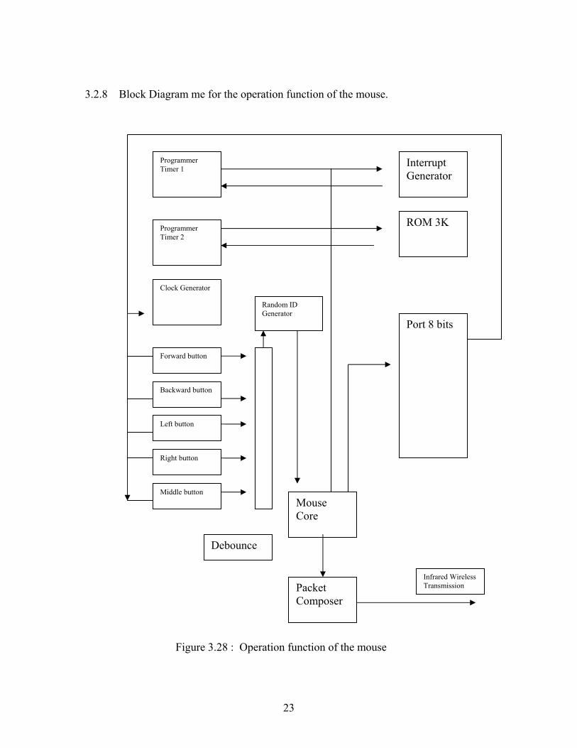
3.2.8 Block Diagram me for the operation function of the mouse.
Figure 3.28 : Operation function of the mouse
Programmer Timer 1
Programmer Timer 2
Clock Generator
Forward button
Backward button
Left button
Right button
Middle button
Debounce
Random ID Generator
Mouse Core
Packet Composer
Port 8 bits
Interrupt Generator
ROM 3K
Infrared Wireless Transmission

24
3.2.9 Quadrature Dimension
The ADNS -2000 is an IC which governs the operation of the mouse. The most
important function of this IC is to Coordinate the quadrature function of the
sensor.The sensor consist of three axis x, y ,z. Where x,y,z is divided into XA,
XB, YA, YB, ZA ,ZB .The purpose of these divided functions is to coordinate the
degree movement of axis x,y,z. As three axis will rotate accordingly in line with
the movement of the mouse sensor.
Below is the IC diagram me for the ADNS-2000:
PS2 PS2
XA
YB
XB
YA
LED
VDD3
REFB
RESET
VDD5
VDD5
GND
OSC2
GND
OSC1
25
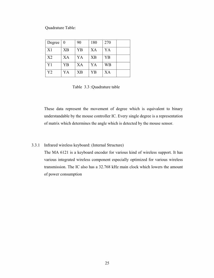
Quadrature Table:
Degree 0 90 180 270
X1 XB YB XA YA
X2 XA YA XB YB
Y1 YB XA YA WB
Y2 YA XB YB XA
Table 3.3 :Quadrature table
These data represent the movement of degree which is equivalent to binary
understandable by the mouse controller IC. Every single degree is a representation
of matrix which determines the angle which is detected by the mouse sensor.
3.3.1 Infrared wireless keyboard: (Internal Structure)
The MA 6121 is a keyboard encoder for various kind of wireless support. It has
various integrated wireless component especially optimized for various wireless
transmission. The IC also has a 32.768 kHz main clock which lowers the amount
of power consumption
26
3.3.2 Features
• Build in keyboard controller
• Seamless sleep mode
• Phantom key detection.
• 32.768 KHz clock rate.
• Internal pull up resistor
• 4k bps baud rate in air
• Internal OSC
• Internal power amplifier
• 20*8 scan lines for all possible key matrices
3.3.3 The keyboard Function:
The function of each key pressed in process is determined by the rows and
columns which is controlled by the IC MA6121.The microcontroller that is used
in this project comprises 18 column and 8 row. Each combination of row and
column represent a button in the keyboard. When a key is pressed, one of row is
made high by making one bit of the output port IC MA6121 high which is
equivalent to “1”.Then the Controller of the input port will detect the suitable
column by referring to the counter. The counter will rotate the information until
the next instruction appear or set.
27
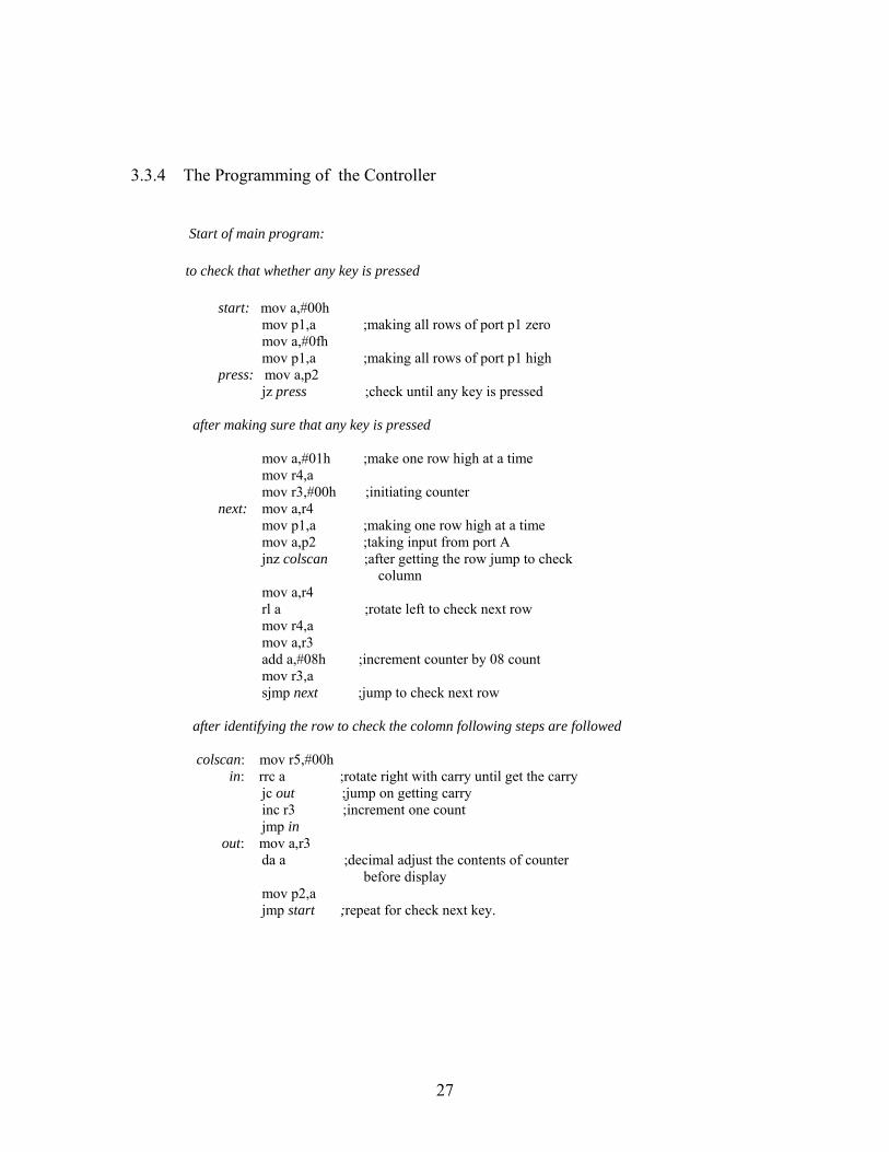
3.3.4 The Programming of the Controller
Start of main program:
to check that whether any key is pressed
start: mov a,#00h mov p1,a ;making all rows of port p1 zero mov a,#0fh mov p1,a ;making all rows of port p1 high press: mov a,p2 jz press ;check until any key is pressed after making sure that any key is pressed mov a,#01h ;make one row high at a time mov r4,a mov r3,#00h ;initiating counter next: mov a,r4 mov p1,a ;making one row high at a time mov a,p2 ;taking input from port A jnz colscan ;after getting the row jump to check column mov a,r4 rl a ;rotate left to check next row mov r4,a mov a,r3 add a,#08h ;increment counter by 08 count mov r3,a sjmp next ;jump to check next row after identifying the row to check the colomn following steps are followed colscan: mov r5,#00h in: rrc a ;rotate right with carry until get the carry jc out ;jump on getting carry inc r3 ;increment one count jmp in out: mov a,r3 da a ;decimal adjust the contents of counter before display mov p2,a jmp start ;repeat for check next key.
28
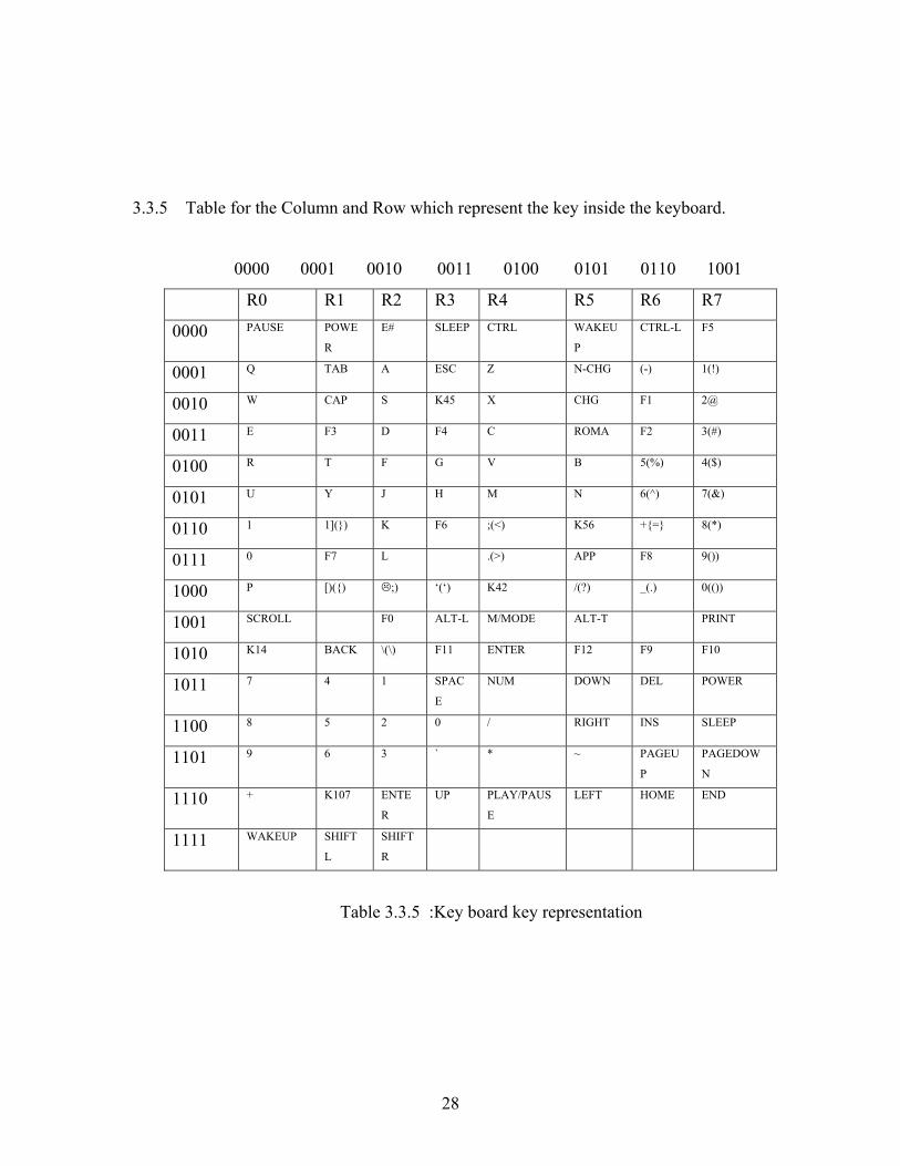
3.3.5 Table for the Column and Row which represent the key inside the keyboard.
0000 0001 0010 0011 0100 0101 0110 1001
R0 R1 R2 R3 R4 R5 R6 R7
0000 PAUSE POWE
R
E# SLEEP CTRL WAKEU
P
CTRL-L F5
0001 Q TAB A ESC Z N-CHG (-) 1(!)
0010 W CAP S K45 X CHG F1 2@
0011 E F3 D F4 C ROMA F2 3(#)
0100 R T F G V B 5(%) 4($)
0101 U Y J H M N 6(^) 7(&)
0110 1 1]() K F6 ;(<) K56 += 8(*)
0111 0 F7 L .(>) APP F8 9())
1000 P [)() ;) ‘(‘) K42 /(?) _(.) 0(())
1001 SCROLL F0 ALT-L M/MODE ALT-T PRINT
1010 K14 BACK \(\) F11 ENTER F12 F9 F10
1011 7 4 1 SPAC
E
NUM DOWN DEL POWER
1100 8 5 2 0 / RIGHT INS SLEEP
1101 9 6 3 ` * ~ PAGEU
P
PAGEDOW
N
1110 + K107 ENTE
R
UP PLAY/PAUS
E
LEFT HOME END
1111 WAKEUP SHIFT
L
SHIFT
R
Table 3.3.5 :Key board key representation
29
3.3.6 Key board priority execute procedure:
Normally the keyboard will prioritize from low to high. For instant a key ‘R’ can
produce CTRL-A ALT- A etc. Under this circumstances the actual state yield of
the controller depends on the modifier key (SHIFT, ALT, CTRL, CAPSLOCK,
NUMLOCK).The controller will prioritize the Alt, following by Ctrl, Shift,
Numlock then finally with the one which is pressed by not accompany by a
modifier key. When the user is pressing one or more modifier key the controller
only identifies the key which have the most priority. For instance the Numlock
and cap lock represent the case status of the key .If this case is pressed and then
the shift key is pressed then the shift key will be inactive.
3.3.7 Special case for modifier key:
There is an exception, not every combination of the modifier key is valid. When
the combination of the modifier key with origin key does match what it is contain
inside the ASCII Codec library the function of the modifier key will be inactive.
For instance CTRL –DOWN. The ISR (information system research) will
generate most of the ASCII for the modifier key, The Legal combination of the
key modifier combination will be determined by the programmed.
30
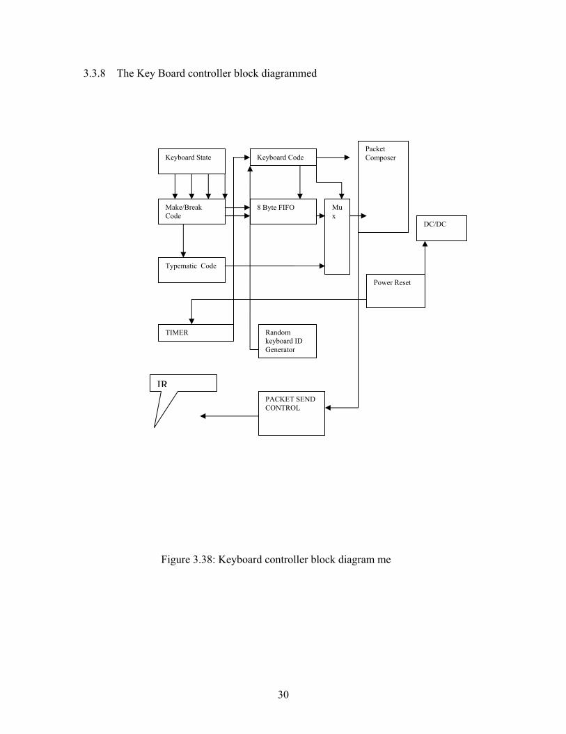
3.3.8 The Key Board controller block diagrammed
Figure 3.38: Keyboard controller block diagram me
Keyboard State
Make/Break Code
Keyboard Code
8 Byte FIFO
Typematic Code
Random keyboard ID Generator
Power Reset
DC/DC
Packet Composer
Mux
TIMER
PACKET SEND CONTROL
IR
31
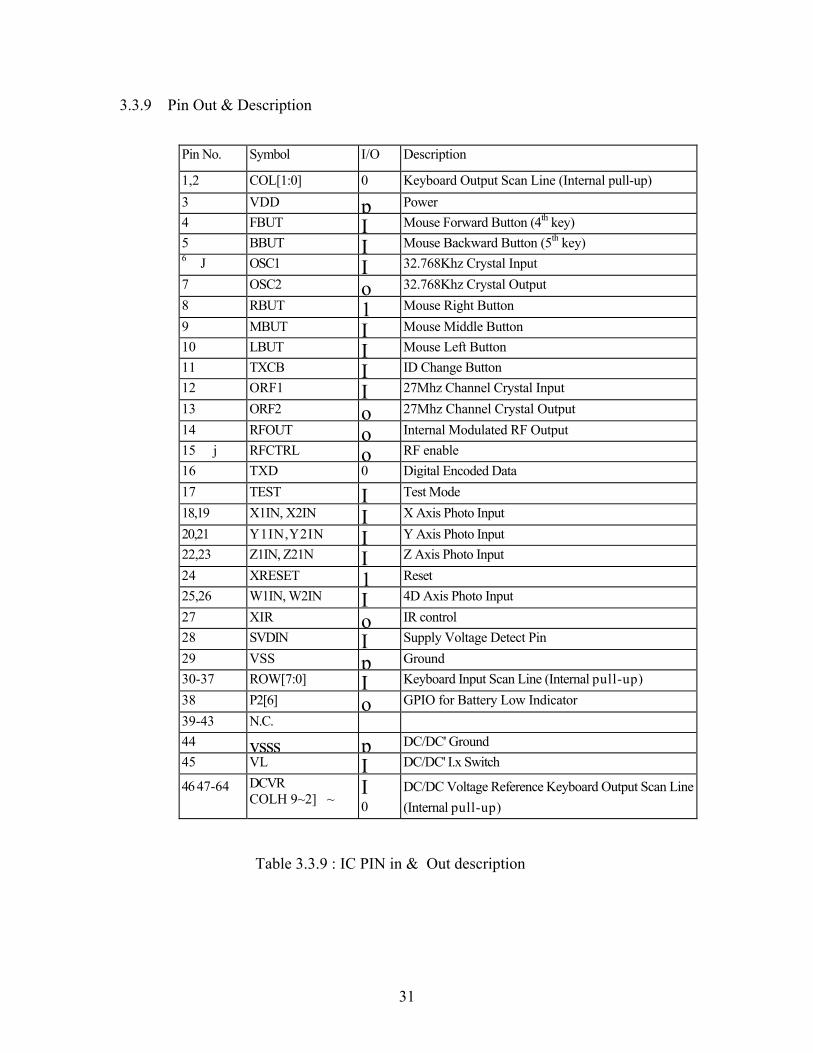
3.3.9 Pin Out & Description
Table 3.3.9 : IC PIN in & Out description
Pin No. Symbol I/O Description
1,2 COL[1:0] 0 Keyboard Output Scan Line (Internal pull-up) 3 VDD p Power 4 FBUT I Mouse Forward Button (4th key) 5 BBUT I Mouse Backward Button (5th key) 6 J OSC1 I 32.768Khz Crystal Input 7 OSC2 o 32.768Khz Crystal Output 8 RBUT 1 Mouse Right Button 9 MBUT I Mouse Middle Button 10 LBUT I Mouse Left Button 11 TXCB I ID Change Button 12 ORF1 I 27Mhz Channel Crystal Input 13 ORF2 o 27Mhz Channel Crystal Output 14 RFOUT o Internal Modulated RF Output 15 j RFCTRL o RF enable 16 TXD 0 Digital Encoded Data 17 TEST I Test Mode 18,19 X1IN, X2IN I X Axis Photo Input 20,21 Y1IN,Y2IN I Y Axis Photo Input 22,23 Z1IN, Z21N I Z Axis Photo Input 24 XRESET 1 Reset 25,26 W1IN, W2IN I 4D Axis Photo Input 27 XIR o IR control 28 SVDIN I Supply Voltage Detect Pin 29 VSS p Ground 30-37 ROW[7:0] I Keyboard Input Scan Line (Internal pull-up) 38 P2[6] o GPIO for Battery Low Indicator 39-43 N.C. 44 vsss p DC/DC' Ground 45 VL I DC/DC' I.x Switch
46 47-64
DCVR COLH 9~2] ~
I 0
DC/DC Voltage Reference Keyboard Output Scan Line (Internal pull-up)
32
3.3.10 Infrared wireless keyboard circuit function
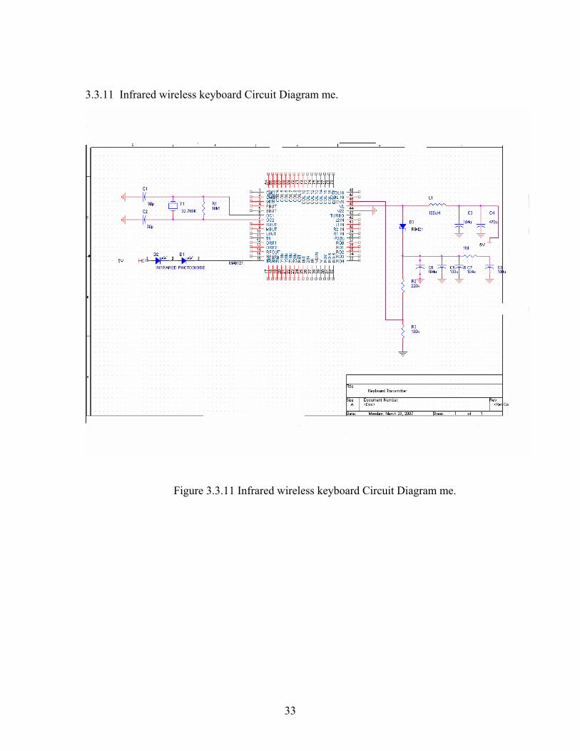
Basically the keyboard circuit consists of several parts. The first parts is the
oscillation 1 and oscillation 2 (OSC1 and OSC2) .Both of these pins are
interconnected, both devices are accompanied and connected by a crystal X1
which has an oscillation frequency of 32768KHz, with a 10 M ohm resistor
interconnected with the 30 piko Farad capacitance in order to generate the upper
and lower critical frequency for the circuit. This set of device will provide
stability timing for the MA6121 to operate in a well manner,
The second part is the TXD pin, the infrared photodiode is attached to this .Two
photodiode is used, the function of the IC MA6121 is designed to operate any
kind of wireless transmission including blue tooth, infrared, RF control.
The third part of the Circuit is the voltage reference pin VL ,the supporting circuit
in the schematic below which consist of several capacitor ,resistor and zener
diode produce and generate a reference voltage in the range of 3-5V in order for
the IC to operate normally. The first row consist of 2 capacitor connected in
parallel which made up a total capacitance of 470U +100U =570U produce a LC
circuit combine with the inductor 100 micro H. Both parts of this will regulate the
voltage and ensure that the voltage supplied are always matched with the
reference voltage as it was set at VL for the IC MA 6121.
33
3.3.11 Infrared wireless keyboard Circuit Diagram me.
Figure 3.3.11 Infrared wireless keyboard Circuit Diagram me.
34
3.4.1 Infrared Receiver for mouse and keyboard
The RF keyboard and mouse controller .In this project we used the MA 6131 IC
which is developed by IBM as a supporting IC for PS2 interface to decode signal
which is send wireless (RF ,Blue Tooth ,Infrared etc). It is a 27MHz receiver for
any kind of wireless transmission. It has a 32.768 KHz main clock to reach quite
low power consumption for the IC
Features of the module:
• Single chip keyboard & mouse controller.
• CPU embedded for keyboard code mapping
• 8K ROM & 128 bytes SRAM
• 32.768KHz clock rate
• 256 ID codes randomly generated to resist interference.
The IC I programmed o decode matrix function received form the keyboard and
the data derived from the mouse. Inside the structure it is divide into two kind of
clock ,the first one is the interrupt generator, and the second one is the clock
Generator. Both clock signal generated should correlate and match each other in
order to produce the right frequency to operate the device.
The Keyboard and the mouse is separately controlled by different clock .Both
device need it on buffer and indicator. After the signal I decoded it I transmitted
and received separately through NRZ moue and NRZ keyboard .The re is a watch
dog timer which reads into the ROM of the IC to check if the programmed timing
executed matches the instruction timer.
35
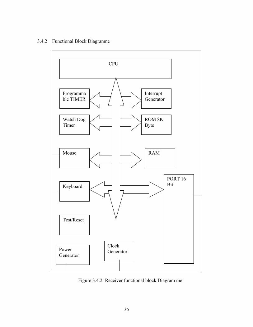
3.4.2 Functional Block Diagramne
Figure 3.4.2: Receiver functional block Diagram me
CPU
Programmable TIMER
Interrupt Generator
Watch Dog Timer
ROM 8K Byte
Mouse RAM
Keyboard
Test/Reset
Clock Generator
PORT 16 Bit
Power Generator
36
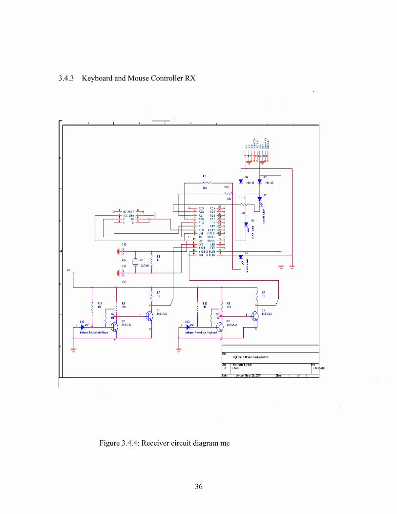
3.4.3 Keyboard and Mouse Controller RX
Figure 3.4.4: Receiver circuit diagram me
37
3.4.4 Keyboard and Mouse Controller RX Circuit Function
1. The 93C46B is a controller for the MA6131.It function as an EEPROM
device which stands for electrical erasable read only memory .This function is
to store new data derived from the device without erasing the prior contents.
Only the bytes and the addresses of the information are updated. The write
operation will take time of the order of several hundred µ/byte. Data derived
from the mouse and keyboard initially stored before processing and
transmitting via infrared.
2. Supporting circuit for the infrared photodiode detector. The circuit consists of
two BC54742 NPN transistors, one 1k resistor .two 10k resistor, and 1 1M
feedback resistor. Both transistor acts as a multistage amplifier arranged in a
direct coupling form. Direct coupling is chosen because the data frequency
derive from the keyboard and mouse can be very low, if a high frequency
device is used, frequency sensitive component like capacitor and transformer
will be needed.
The Dc output will appear in the input of the next stage. When the signal is
applied to the input of the first transistor the amplified output appear at the
collector of the second transistor. The amplified output becomes the base
signal for second transistor the further amplification is the multiplication of
the first stage current gain and the second stage current gain. The resistor
1MΩ acts as a compensation circuit to reduce the drift of the operating point,
and provide excellent bias and good stabilization. The 10kΩ resistor
connected next to the infrared photodetector serve as a load resistance to
switch the device on and off in nanosecond range for both rise time and fall
time
38
3. The CN1A is the frequency regulator that generates the signal for each
instruction being executed by the mouse and keyboard govern by a clock
frequency implanted inside the device. There are three indicator diodes which
indicate the scroll status of the mouse and cap lock ,Numlock for the mouse.
4. An oscillator is used to generate the right clock frequency from the crystal ,to
ensure that the IC will work properly.
5. A DC 9V battery is used in this device as the active component .
3.5.1 Infrared Printer
The transfer rate of a normal printer usually is about1.5mbps..Wheares the
infrared transmission is between 30-40KHz..Initially I have tried to convert the
ATMEL IC wireless module into infrared wireless. But the Amtel did not support
the instruction send by the printer.
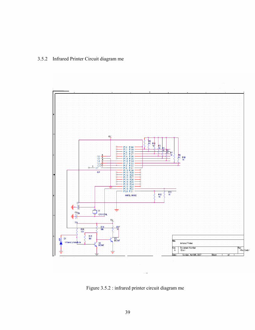
Then the communication port which connect the printer to the transmitter is
connected to the parallel port .8 bits of the transmitter is used from pin 32 toward
pin39.Each output port from pin 32-39 is accompanied by a pull up resistor of
1kΩ to pull up its voltage before it is being transmitted to the parallel port
There is an indicator which is connected to pin 22 and 21 to indicate the status of
the printer. The indicator is determine is determine by binary 0 and 1.If 1 occur in
pin 22 it means that the printer is in stable mode, if bone occur in pin 21 it means
the printer is in the busy mode Only when 10 occur for both pin 22 ,21 the printer
can start transmitting signal
Then a crystal is connected to the pin 18 and 19 to ensure that the IC is working
on the right mode.
The ISP port is connected to load low level programming form the computer to
control the printer transmission. Then the pin 10 is connected with a direct
coupling transistor to invert signal The coupling circuit that is used as a
supporting circuit to the photodiode is exactly the same as what is used for the
keyboard and mouse
39
3.5.2 Infrared Printer Circuit diagram me
Figure 3.5.2 : infrared printer circuit diagram me
40
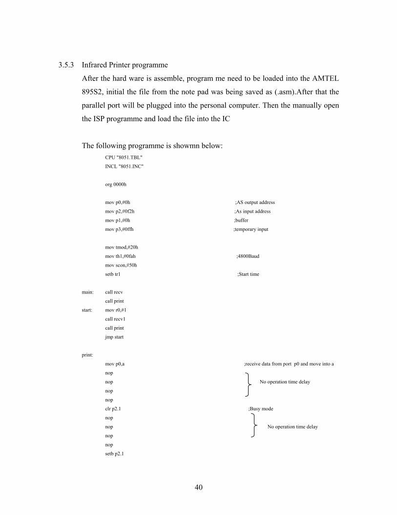
3.5.3 Infrared Printer programme
After the hard ware is assemble, program me need to be loaded into the AMTEL
895S2, initial the file from the note pad was being saved as (.asm).After that the
parallel port will be plugged into the personal computer. Then the manually open
the ISP programme and load the file into the IC
The following programme is showmn below: CPU "8051.TBL"
INCL "8051.INC"
org 0000h
mov p0,#0h ;AS output address
mov p2,#0f2h ;As input address
mov p1,#0h ;buffer
mov p3,#0ffh ;temporary input
mov tmod,#20h
mov th1,#0fah ;4800Baud
mov scon,#50h
setb tr1 ;Start time
main: call recv
call print
start: mov r0,#1
call recv1
call print
jmp start
print:
mov p0,a ;receive data from port p0 and move into a
nop
nop No operation time delay
nop
nop
clr p2.1 ;Busy mode
nop
nop No operation time delay
nop
nop
setb p2.1
41
ack: jb p2.0,ack ;jump if bit high
ret
finish:
mov a,#12 ;Command paper out count
call print
jmp main
recv1: inc r0
call delay1
cjne r0,#255,con1
jmp finish
con1: jnb ri,recv1
mov a,sbuf
clr ri
ret
recv: jnb ri,recv
mov a,sbuf
clr ri
ret
delay1:
mov r7,#10
again2: mov r6,#50
again3: djnz r6,again3
djnz r7,again2
ret
end
42
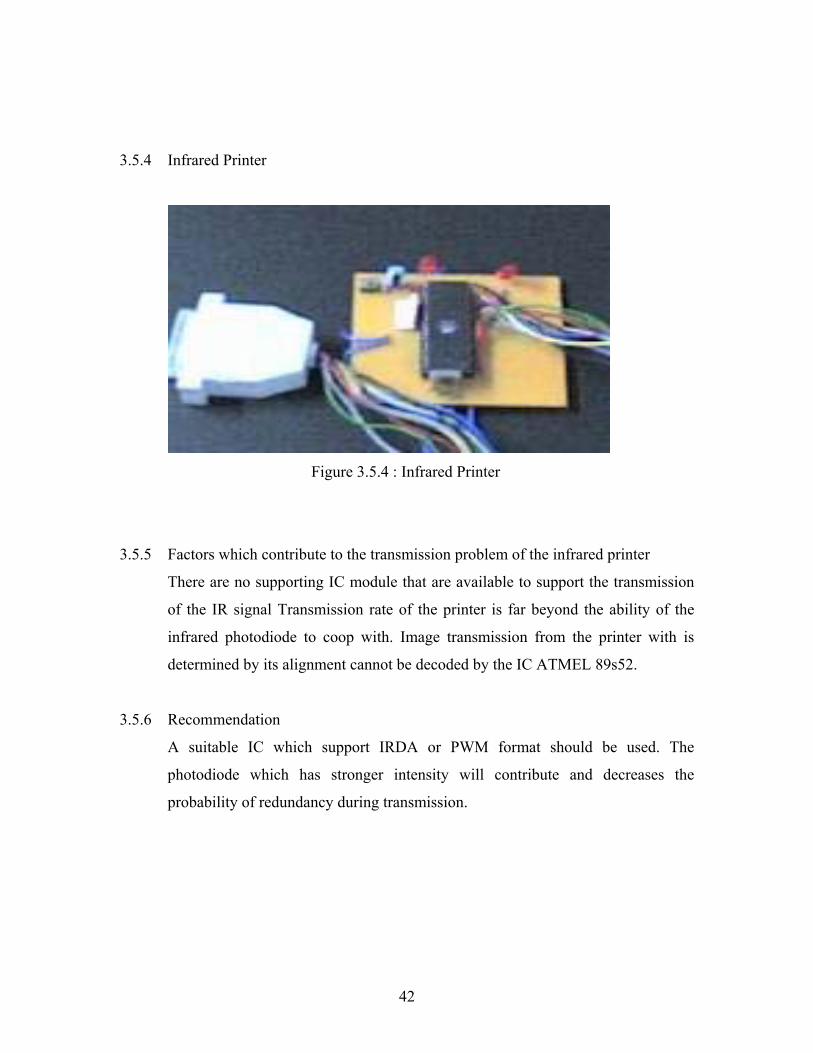
3.5.4 Infrared Printer
Figure 3.5.4 : Infrared Printer
3.5.5 Factors which contribute to the transmission problem of the infrared printer
There are no supporting IC module that are available to support the transmission
of the IR signal Transmission rate of the printer is far beyond the ability of the
infrared photodiode to coop with. Image transmission from the printer with is
determined by its alignment cannot be decoded by the IC ATMEL 89s52.
3.5.6 Recommendation
A suitable IC which support IRDA or PWM format should be used. The
photodiode which has stronger intensity will contribute and decreases the
probability of redundancy during transmission.


![CHAPTER 2 LITERATURE REVIEW - Universiti …dspace.unimap.edu.my/dspace/bitstream/123456789/3108/5/Literature... · CHAPTER 2 LITERATURE REVIEW ... WinForm. [1] 2.3 What is ... The](https://img.pdfslide.us/doc/110x75/5b8169c57f8b9ae97b8c40d3/chapter-2-literature-review-universiti-chapter-2-literature-review-winform.jpg)