Embed Size (px)
Citation preview

Charles Kime & Thomas Kaminski
© 2008 Pearson Education, Inc.(Hyperlinks are active in View Show mode)
Chapter 3 – Combinational Logic Design
Part 1 – Implementation Technology and Logic Design
Logic and Computer Design Fundamentals

Chapter 3 - Part 1 2
Overview
Part 1 – Design Procedure
• Steps Specification
Formulation
Optimization
Technology Mapping
• Beginning Hierarchical Design
• Technology Mapping - AND, OR, and NOT to NAND or NOR
• Verification Manual
Simulation
Chapter 3 - Part 1 3
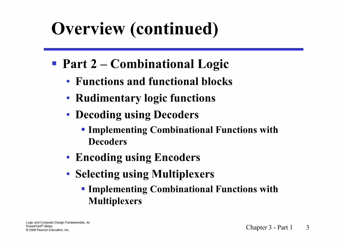
Overview (continued)
Part 2 – Combinational Logic
• Functions and functional blocks
• Rudimentary logic functions
• Decoding using Decoders
Implementing Combinational Functions with Decoders
• Encoding using Encoders
• Selecting using Multiplexers
Implementing Combinational Functions with Multiplexers
Chapter 3 - Part 1 4
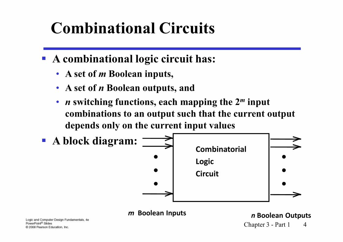
Combinational Circuits
A combinational logic circuit has:
• A set of m Boolean inputs,
• A set of n Boolean outputs, and
• n switching functions, each mapping the 2m input combinations to an output such that the current output depends only on the current input values
A block diagram:
m Boolean Inputs n Boolean Outputs
Combinatorial
Logic
Circuit

Chapter 3 - Part 1 5
Design Procedure
1. Specification• Write a specification for the circuit if one is not
already available
2. Formulation• Derive a truth table or initial Boolean equations
that define the required relationships between the inputs and outputs, if not in the specification
• Apply hierarchical design if appropriate
3. Optimization• Apply 2-level and multiple-level optimization
• Draw a logic diagram or provide a netlist for the resulting circuit using ANDs, ORs, and inverters
Chapter 3 - Part 1 6
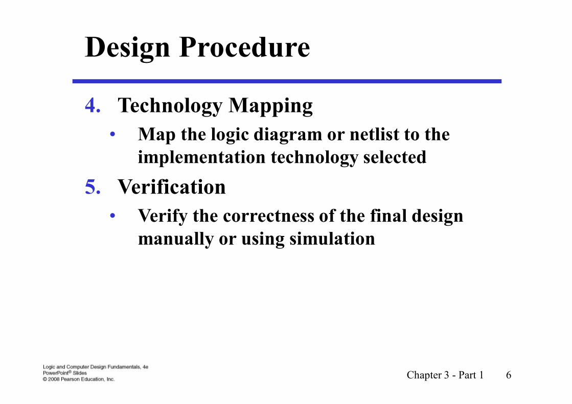
Design Procedure
4. Technology Mapping
• Map the logic diagram or netlist to the implementation technology selected
5. Verification
• Verify the correctness of the final design manually or using simulation
Chapter 3 - Part 1 7
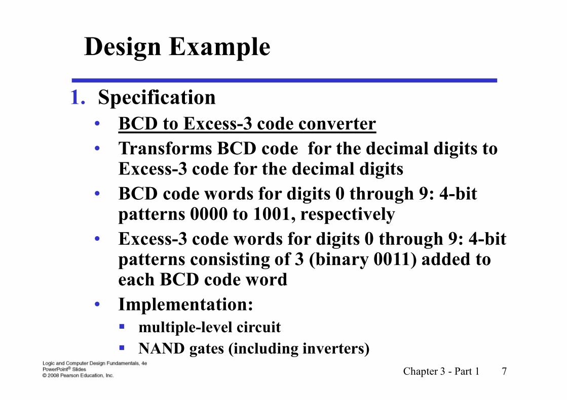
Design Example
1. Specification • BCD to Excess-3 code converter
• Transforms BCD code for the decimal digits to Excess-3 code for the decimal digits
• BCD code words for digits 0 through 9: 4-bit patterns 0000 to 1001, respectively
• Excess-3 code words for digits 0 through 9: 4-bit patterns consisting of 3 (binary 0011) added to each BCD code word
• Implementation: multiple-level circuit
NAND gates (including inverters)
Chapter 3 - Part 1 8
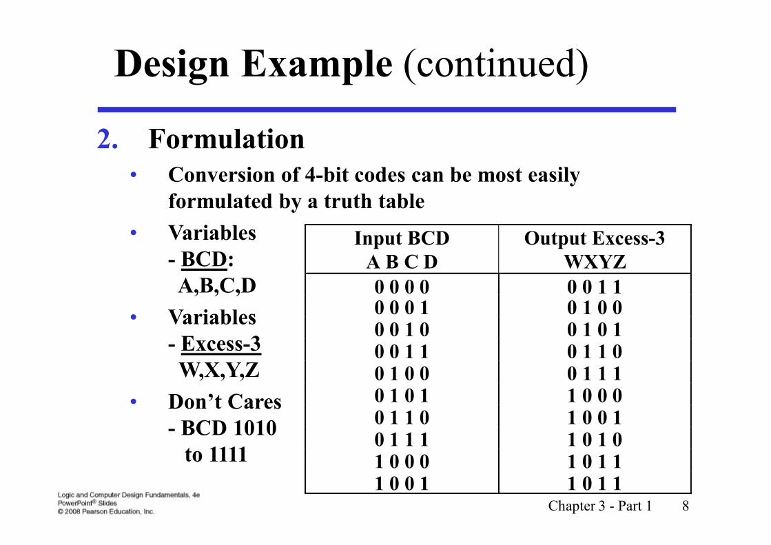
Design Example (continued)
2. Formulation• Conversion of 4-bit codes can be most easily
formulated by a truth table
• Variables- BCD:A,B,C,D
• Variables- Excess-3W,X,Y,Z
• Don’t Cares- BCD 1010
to 1111
Input BCD A B C D
Output Excess-3 WXYZ
0 0 0 0 0 0 1 1 0 0 0 1 0 1 0 0 0 0 1 0 0 1 0 1 0 0 1 1 0 1 1 0 0 1 0 0 0 1 1 1 0 1 0 1 1 0 0 0 0 1 1 0 1 0 0 1 0 1 1 1 1 0 1 0 1 0 0 0 1 0 1 1 1 0 0 1 1 0 1 1

Chapter 3 - Part 1 9
Design Example (continued)
3. Optimization
a. 2-level usingK-maps
W = A + BC + BD
X = C + D + B
Y = CD +
Z =
B
C
D
A
0 1 3 2
4 5 7 6
12 13 15 14
8 9 11 10
1
11
1
X X X
X X
X
1
B
C
D
A
0 1 3 2
4 5 7 6
12 13 15 14
8 9 11 10
1
11
1
X X X
X X
X
1
B
C
D
A
0 1 3 2
4 5 7 6
12 13 15 14
8 9 11 10
1 1
1
1
X X X
X X
X
1
B
C
D
A
0 1 3 2
4 5 7 6
12 13 15 14
8 9 11 10
1 1
1
X X X
X X
X
1
1
w
z y
x
B CDB
CD
D
Chapter 3 - Part 1 10
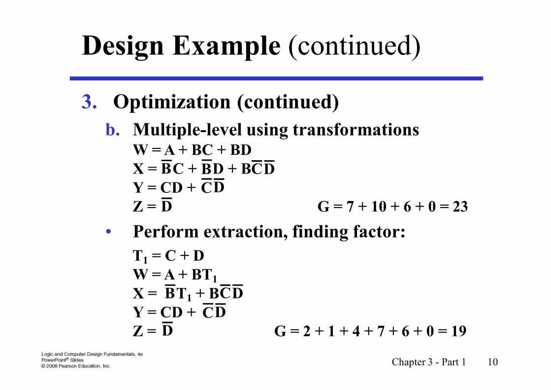
Design Example (continued)
3. Optimization (continued)
b. Multiple-level using transformationsW = A + BC + BDX = C + D + BY = CD + Z = G = 7 + 10 + 6 + 0 = 23
• Perform extraction, finding factor:
T1 = C + DW = A + BT1
X = T1 + BY = CD + Z = G = 2 + 1 + 4 + 7 + 6 + 0 = 19
B CDBCD
D
B CDCD
D
Chapter 3 - Part 1 11
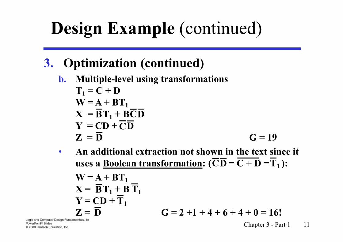
Design Example (continued)
3. Optimization (continued)b. Multiple-level using transformations
T1 = C + DW = A + BT1
X = T1 + BY = CD + Z = G = 19
• An additional extraction not shown in the text since it uses a Boolean transformation: ( = C + D = ):
W = A + BT1
X = T1 + B Y = CD + Z = G = 2 +1 + 4 + 6 + 4 + 0 = 16!
B CDCD
D
B T1
DT1
CD T1
Chapter 3 - Part 1 12
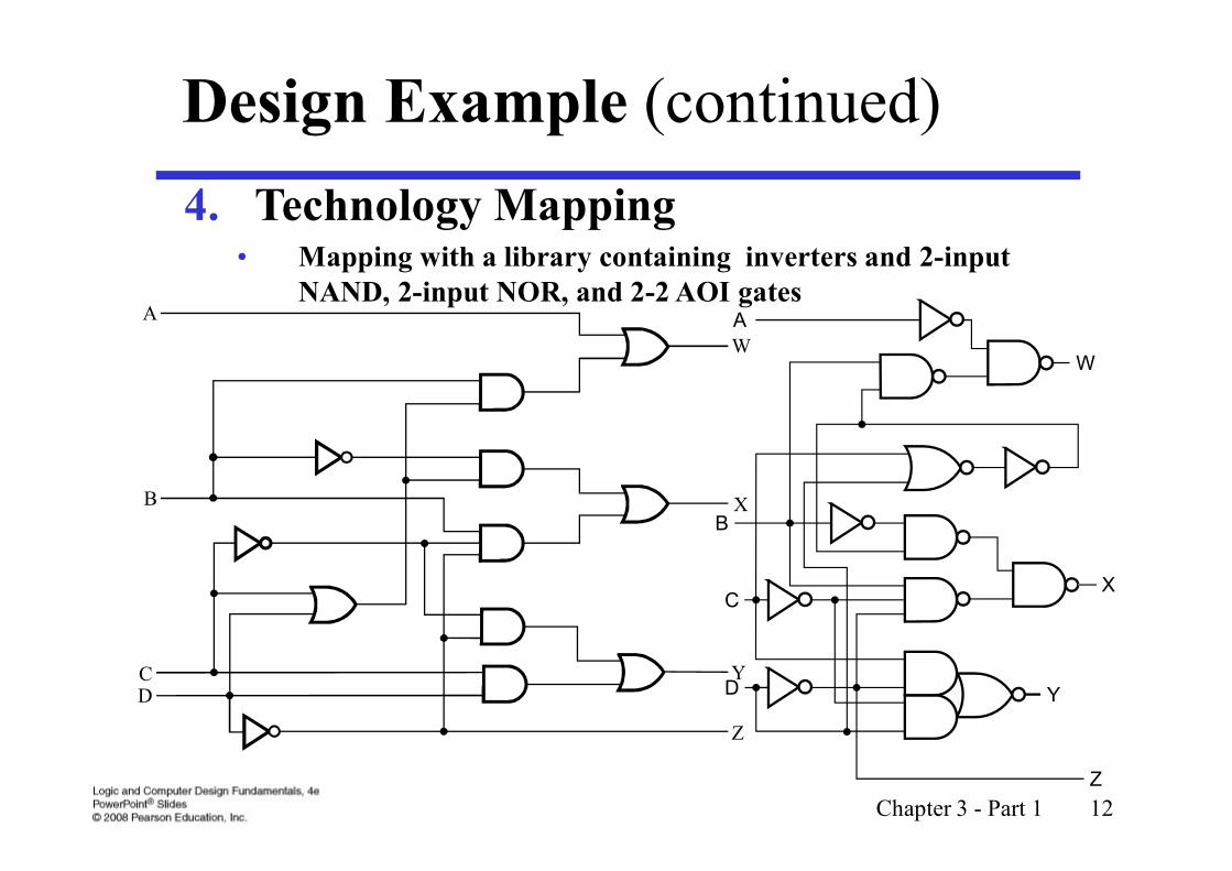
Design Example (continued)
4. Technology Mapping • Mapping with a library containing inverters and 2-input
NAND, 2-input NOR, and 2-2 AOI gates A
B
C
D
W
X
Y
Z
A
B
CD
W
X
Y
Z

Chapter 3 - Part 1 13
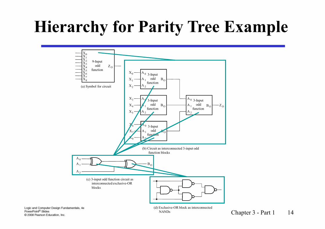
Beginning Hierarchical Design
To control the complexity of the function mapping inputs to outputs: • Decompose the function into smaller pieces called blocks
• Decompose each block’s function into smaller blocks, repeating as necessary until all blocks are small enough
• Any block not decomposed is called a primitive block
• The collection of all blocks including the decomposed ones is a hierarchy
Example: 9-input parity tree (see next slide)• Top Level: 9 inputs, one output
• 2nd Level: Four 3-bit odd parity trees in two levels
• 3rd Level: Two 2-bit exclusive-OR functions
• Primitives: Four 2-input NAND gates
• Design requires 4 X 2 X 4 = 32 2-input NAND gates
Chapter 3 - Part 1 14
Hierarchy for Parity Tree Example
BO
X0X1X2X3X4X5X6X7X8
Z O
9-Inputodd
function
(a) Symbol for circuit
3-Inputodd
function
A 0
A 1
A 2
BO
3-Inputodd
function
A 0
A 1
A 2
BO
3-Inputodd
function
A 0
A 1
A 2
BO
3-Inputodd
function
A 0
A 1
A 2
X0
X1
X2
X3
X4
X5
X6
X7
X8
Z O
(b) Circuit as interconnected 3-input oddfunction blocks
BO
A 0
A 1
A 2
(c) 3-input odd function circuit asinterconnected exclusive-ORblocks
(d) Exclusive-OR block as interconnectedNANDs

Chapter 3 - Part 1 15
Reusable Functions
Whenever possible, we try to decompose a complex design into common, reusablefunction blocks
These blocks are
• verified and well-documented
• placed in libraries for future use
Chapter 3 - Part 1 16
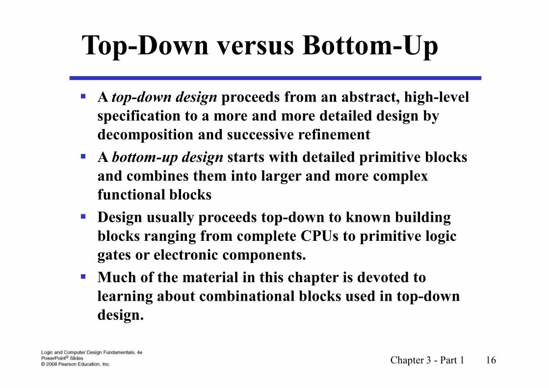
Top-Down versus Bottom-Up
A top-down design proceeds from an abstract, high-level specification to a more and more detailed design by decomposition and successive refinement
A bottom-up design starts with detailed primitive blocks and combines them into larger and more complex functional blocks
Design usually proceeds top-down to known building blocks ranging from complete CPUs to primitive logic gates or electronic components.
Much of the material in this chapter is devoted to learning about combinational blocks used in top-down design.
Chapter 3 - Part 1 17
Technology Mapping
Mapping Procedures
• To NAND gates
• To NOR gates
• Mapping to multiple types of logic blocks in covered in the reading supplement: Advanced Technology Mapping.

Chapter 3 - Part 1 18
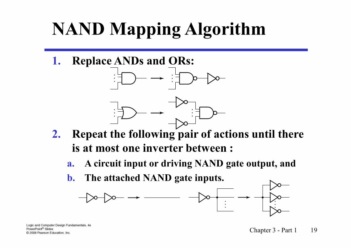
Mapping to NAND gates
Assumptions:• Gate loading and delay are ignored
• Cell library contains an inverter and n-input NAND gates, n = 2, 3, …
• An AND, OR, inverter schematic for the circuit is available
The mapping is accomplished by:• Replacing AND and OR symbols,
• Pushing inverters through circuit fan-out points, and
• Canceling inverter pairs
Chapter 3 - Part 1 19
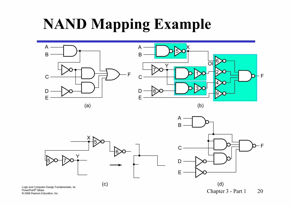
NAND Mapping Algorithm
1. Replace ANDs and ORs:
2. Repeat the following pair of actions until there is at most one inverter between :
a. A circuit input or driving NAND gate output, and
b. The attached NAND gate inputs.
.
.
....
.
.
....
.
.
....
Chapter 3 - Part 1 20
NAND Mapping Example
A
B
C
D
F
E
(a)
A
B
C
7
5
1
6
2
4
9
X
Y
38D
E
F
(b)
A
B
C
D
E
F
(d)
X
5
5
7
6Y
(c)
OI
Chapter 3 - Part 1 21
Mapping to NOR gates
Assumptions:• Gate loading and delay are ignored
• Cell library contains an inverter and n-input NOR gates, n = 2, 3, …
• An AND, OR, inverter schematic for the circuit is available
The mapping is accomplished by:• Replacing AND and OR symbols,
• Pushing inverters through circuit fan-out points, and
• Canceling inverter pairs
Chapter 3 - Part 1 22
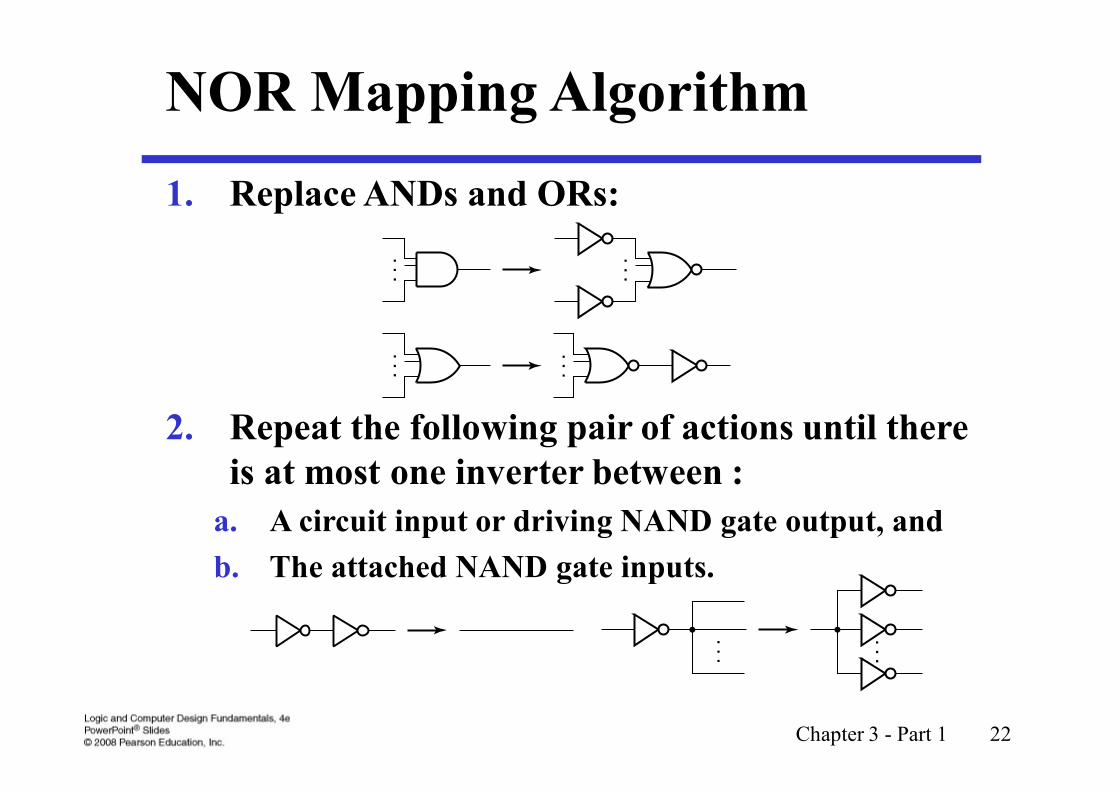
NOR Mapping Algorithm
1. Replace ANDs and ORs:
2. Repeat the following pair of actions until there is at most one inverter between :
a. A circuit input or driving NAND gate output, and
b. The attached NAND gate inputs.
.
.
....
.
.
.
.
.
....
.
.
.
Chapter 3 - Part 1 23
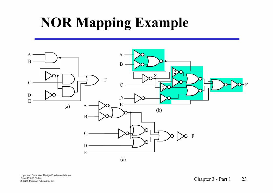
NOR Mapping Example
A
B
C
D
E
F
(c)
F
A
B
X
C
D
E(b)
A
B
C
DE
F
(a)
2
3
1

Chapter 3 - Part 1 24
Verification - show that the final circuit designed implements the original specification
Simple specifications are:
• truth tables
• Boolean equations
• HDL code
If the above result from formulation and are not the original specification, it is critical that the formulation process be flawless for the verification to be valid!
Verification
Chapter 3 - Part 1 25
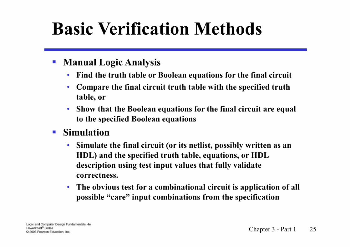
Basic Verification Methods
Manual Logic Analysis• Find the truth table or Boolean equations for the final circuit
• Compare the final circuit truth table with the specified truth table, or
• Show that the Boolean equations for the final circuit are equal to the specified Boolean equations
Simulation• Simulate the final circuit (or its netlist, possibly written as an
HDL) and the specified truth table, equations, or HDL description using test input values that fully validate correctness.
• The obvious test for a combinational circuit is application of all possible “care” input combinations from the specification
Chapter 3 - Part 1 26
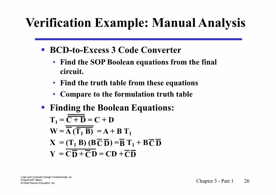
Verification Example: Manual Analysis
BCD-to-Excess 3 Code Converter
• Find the SOP Boolean equations from the final circuit.
• Find the truth table from these equations
• Compare to the formulation truth table
Finding the Boolean Equations:
T1 = C + D = C + D
W = A (T1 B) = A + B T1
X = (T1 B) (B ) = T1 + B
Y = C + D = CD + D
C D
C
B C D
CD
Chapter 3 - Part 1 27
Input BCDA B C D
Output Excess-3WXYZ
0 0 0 0 0 0 1 10 0 0 1 0 1 0 00 0 1 0 0 1 0 10 0 1 1 0 1 1 00 1 0 0 0 1 1 10 1 0 1 1 0 0 00 1 1 0 1 0 0 10 1 1 1 1 0 1 01 0 0 0 1 0 1 11 0 0 1 1 0 1 1
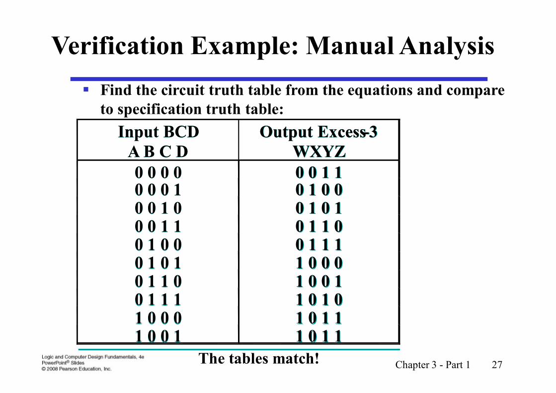
Verification Example: Manual Analysis
Find the circuit truth table from the equations and compare to specification truth table:
The tables match!
Input BCDA B C D
Output Excess-3WXYZ
0 0 0 0 0 0 1 10 0 0 1 0 1 0 00 0 1 0 0 1 0 10 0 1 1 0 1 1 00 1 0 0 0 1 1 10 1 0 1 1 0 0 00 1 1 0 1 0 0 10 1 1 1 1 0 1 01 0 0 0 1 0 1 11 0 0 1 1 0 1 1
Chapter 3 - Part 1 28
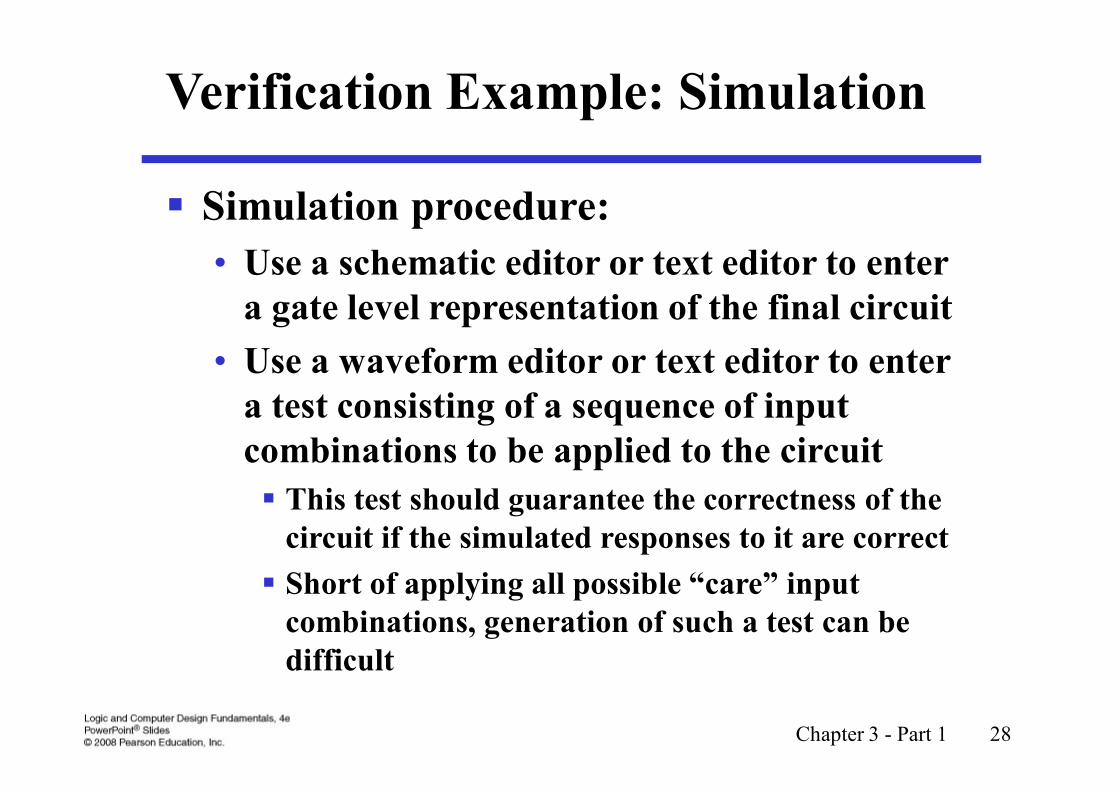
Verification Example: Simulation
Simulation procedure:
• Use a schematic editor or text editor to enter a gate level representation of the final circuit
• Use a waveform editor or text editor to enter a test consisting of a sequence of input combinations to be applied to the circuit
This test should guarantee the correctness of the circuit if the simulated responses to it are correct
Short of applying all possible “care” input combinations, generation of such a test can be difficult
Chapter 3 - Part 1 29
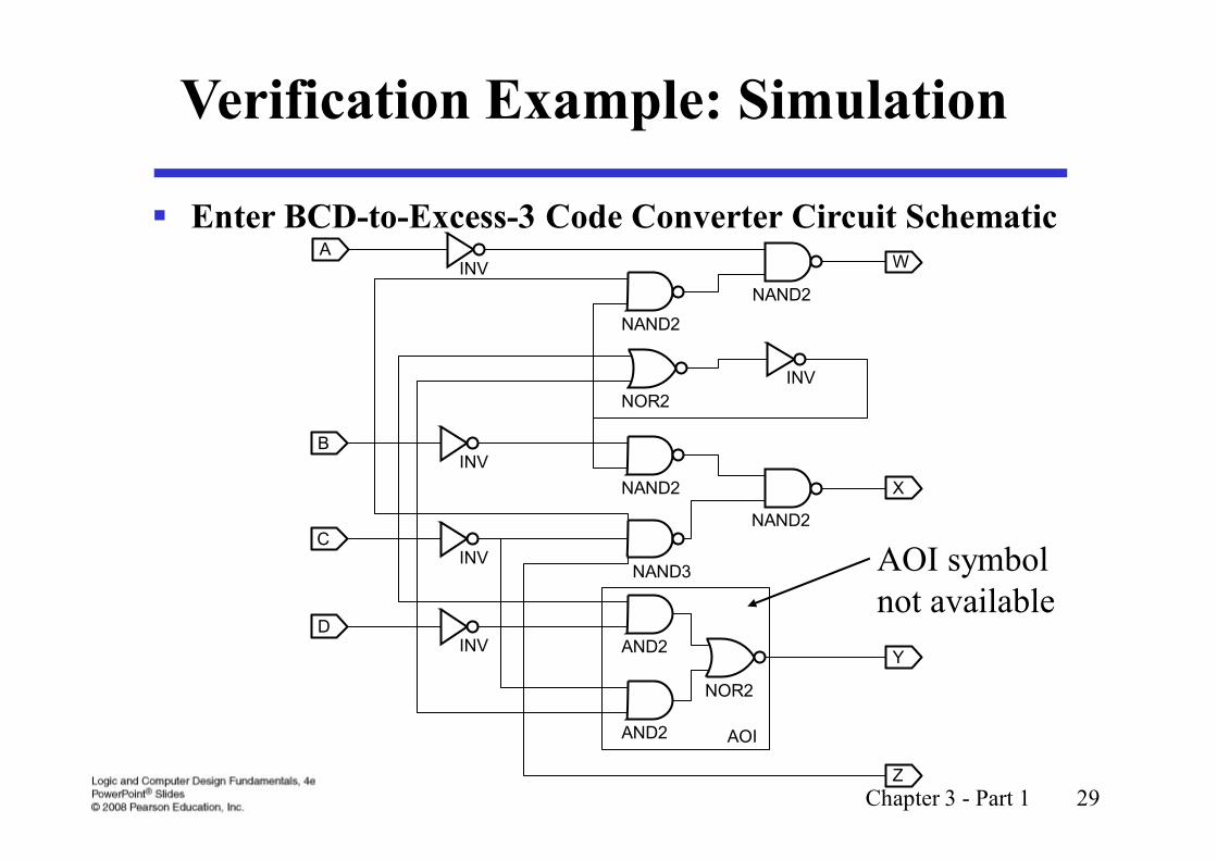
Verification Example: Simulation
Enter BCD-to-Excess-3 Code Converter Circuit Schematic
NAND2
NAND2
INV
NOR2
INV
NAND2
INV
NAND2
AND2
AND2
NAND3INV
INV
NOR2
W
B
A
C
D
X
AOI
Y
Z
AOI symbolnot available
Chapter 3 - Part 1 30
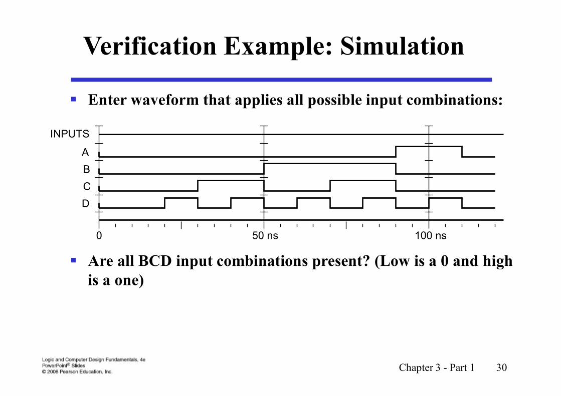
Verification Example: Simulation
Enter waveform that applies all possible input combinations:
Are all BCD input combinations present? (Low is a 0 and high is a one)
0 50 ns 100 ns
INPUTS
A
B
C
D
Chapter 3 - Part 1 31
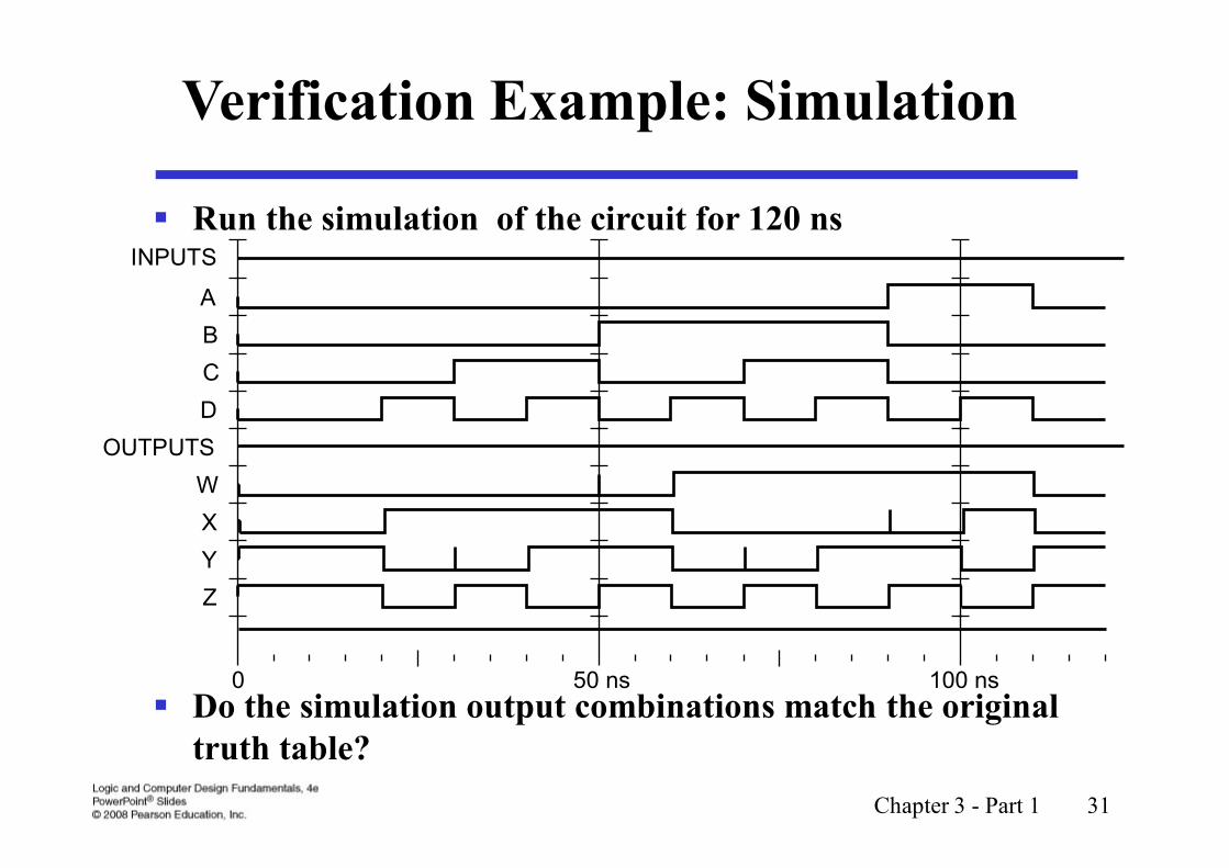
Verification Example: Simulation
Run the simulation of the circuit for 120 ns
Do the simulation output combinations match the original truth table?
0 50 ns 100 ns
INPUTS
A
B
C
D
OUTPUTS
W
X
Y
Z
Chapter 3 - Part 1 32
Terms of Use
All (or portions) of this material © 2008 by Pearson Education, Inc.
Permission is given to incorporate this material or adaptations thereof into classroom presentations and handouts to instructors in courses adopting the latest edition of Logic and Computer Design Fundamentals as the course textbook.
These materials or adaptations thereof are not to be sold or otherwise offered for consideration.
This Terms of Use slide or page is to be included within the original materials or any adaptations thereof.