Embed Size (px)
Citation preview
24
CHAPTER 2
TRIAC BASED SCHEMES - AN OVERVIEW
2.1 INTRODUCTION
This chapter depicts the principle of operation and working of the
triac based methods used for the speed control of the fan motor and their
drawbacks. It also discusses the simulation and experimental study of this scheme.
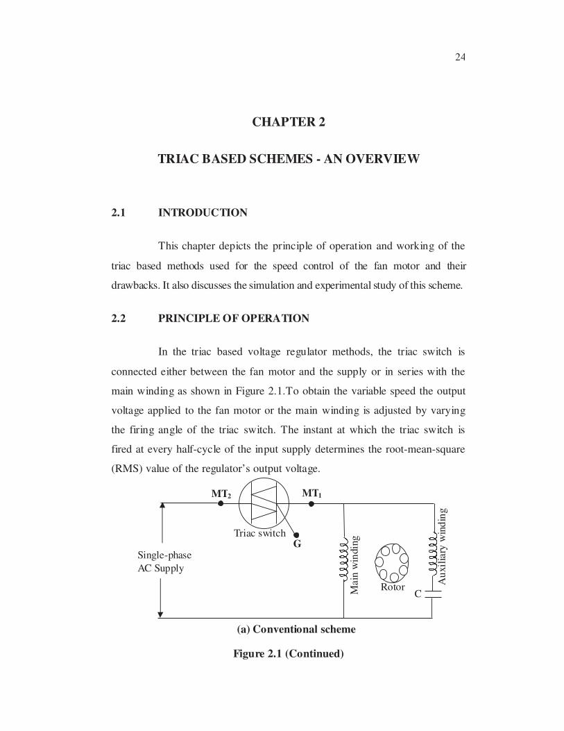
2.2 PRINCIPLE OF OPERATION
In the triac based voltage regulator methods, the triac switch is
connected either between the fan motor and the supply or in series with the
main winding as shown in Figure 2.1.To obtain the variable speed the output
voltage applied to the fan motor or the main winding is adjusted by varying
the firing angle of the triac switch. The instant at which the triac switch is
fired at every half-cycle of the input supply determines the root-mean-square
(RMS) value of the regulator’s output voltage.
(a) Conventional scheme
Figure 2.1 (Continued)
Mai
n w
indi
ng
Rotor Au
xili
ary
win
din
g
C
Single-phase
AC Supply
G
MT2 MT1
Triac switch
25
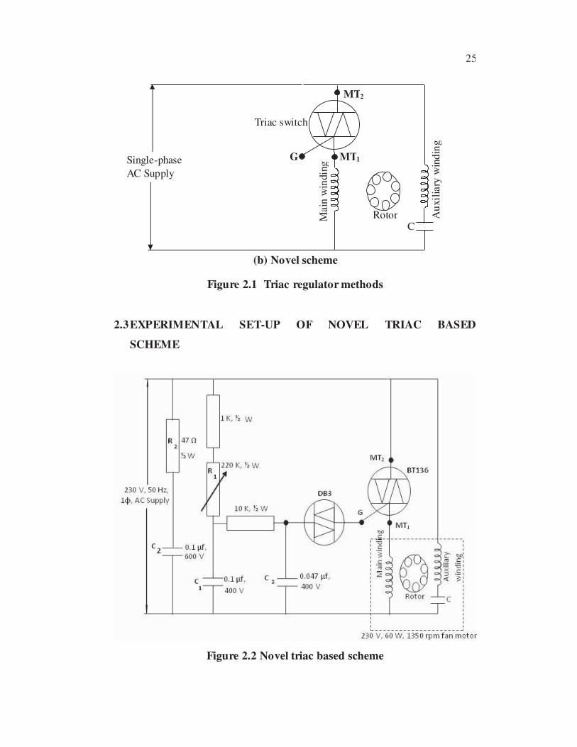
(b) Novel scheme
Figure 2.1 Triac regulator methods
2.3EXPERIMENTAL SET-UP OF NOVEL TRIAC BASED
SCHEME
Figure 2.2 Novel triac based scheme
Mai
n w
indi
ng
Rotor Au
xili
ary
win
din
g
C
Single-phase
AC Supply
G
MT2
MT1
Triac switch
26
Unlike the traditional one, in the novel scheme (Sundareswaran
2001) only the voltage across the main winding is varied and hence the speed.
The auxiliary winding voltage is directly fed from the supply and it is
maintained at the rated voltage.
In the circuit shown in Figure 2.2, the triac is fired with the help of
diac by means of R-C triggering process. R1 and C1 form the R-C network for
triggering. When the voltage across the capacitor of the R-C network is equal
to or more than the break-over voltage of the diac, it starts conducting and
thus fires the triac. The firing angle of the triac can be varied by changing the
value of the ‘R1’ (in the R-C network) with the help of the potentiometer.
Depending upon the firing angle of the triac, the speed of the fan motor will
vary. Less the value of the firing angle of the triac, more will be the voltage
across the main winding of the fan motor and hence higher will be the speed
and vice-versa.
During the positive half-cycle of the input supply, the triac requires
positive gate pulse to turn ON. When voltage across C1 equals or exceeds the
break-over voltage of the diac, the diac breaks down and a positive pulse is
applied to trigger the triac gate. A similar operation will take place in the
negative half-cycle of the supply and therefore, a negative gate pulse is
applied when the diac breaks down in the reverse direction. R2 and C2 form
the snubber circuit and it is used to suppress the transients appearing in the
input mains supply. The capacitor C3 is used as a filter.
2.4 ANALYSIS OF NOVEL TRIAC BASED SCHEME
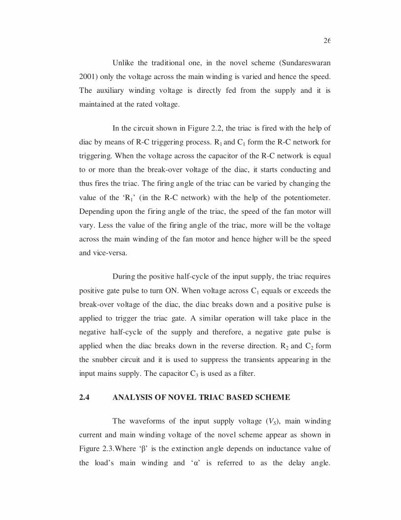
The waveforms of the input supply voltage (VS), main winding
current and main winding voltage of the novel scheme appear as shown in
Figure 2.3.Where ‘ ’ is the extinction angle depends on inductance value of
the load’s main winding and ‘ ’ is referred to as the delay angle.
27
Discontinuous load current operation occurs for and . The
main winding impedance angle is governed by the expression as follows:
1tan
L
R(2.1)
L and R in the expression refer to main winding inductance and
resistance respectively. The main winding impedance angle (Ø) is determined
as 49.79° in the case of motor taken up for study. The extinction angle ‘ ’ can
be determined from the following transcendental equation by using the
iterative method of solution (trial and error method).
sin sinR
Le (2.2)
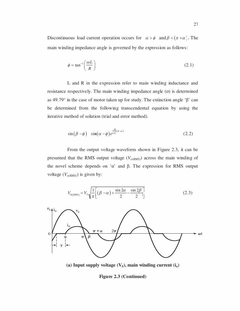
From the output voltage waveform shown in Figure 2.3, it can be
presumed that the RMS output voltage (Vo(RMS)) across the main winding of
the novel scheme depends on ‘ ’ and . The expression for RMS output
voltage (Vo(RMS)) is given by:
1 sin 2 sin 2
2 2SO RMS
V V (2.3)
(a) Input supply voltage (VS), main winding current (io)
Figure 2.3 (Continued)
28
(b) Main winding voltage (Vo)
Figure 2.3 Typical waveforms of novel scheme
Table 2.1 Comparison of RMS output voltages – Novel triac based
scheme
(deg) (deg)
RMS output voltage (Vo(RMS))
Theoretical
(V)
Simulated
(V)
Measured
(V)
90° 224.675° 176.49 180 177
110° 219.85° 136.01 139.5 138
120° 216.655° 114.19 118 116
135° 210.815° 80.22 82 80
The calculated, simulated and measured values of RMS output
voltage across the main winding with novel triac scheme are compared for
validation as shown in Table 2.1. It is observed that all the aforesaid values
are close to each other for given value of delay angle ( ).
29
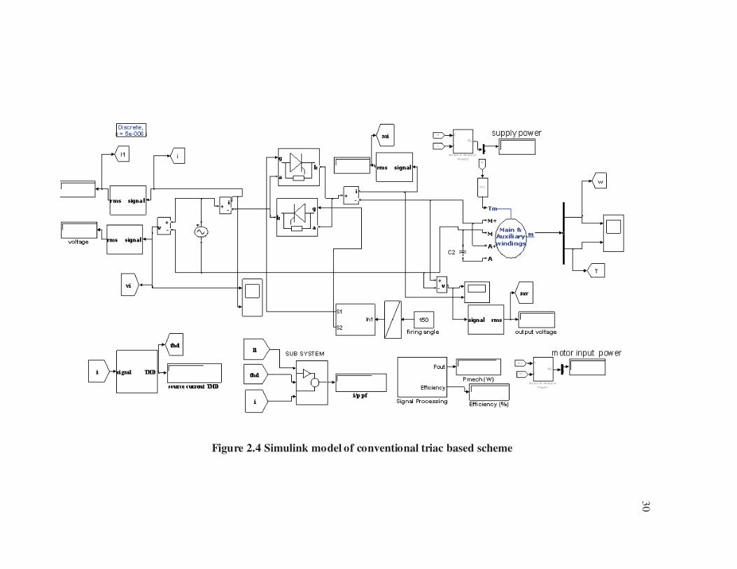
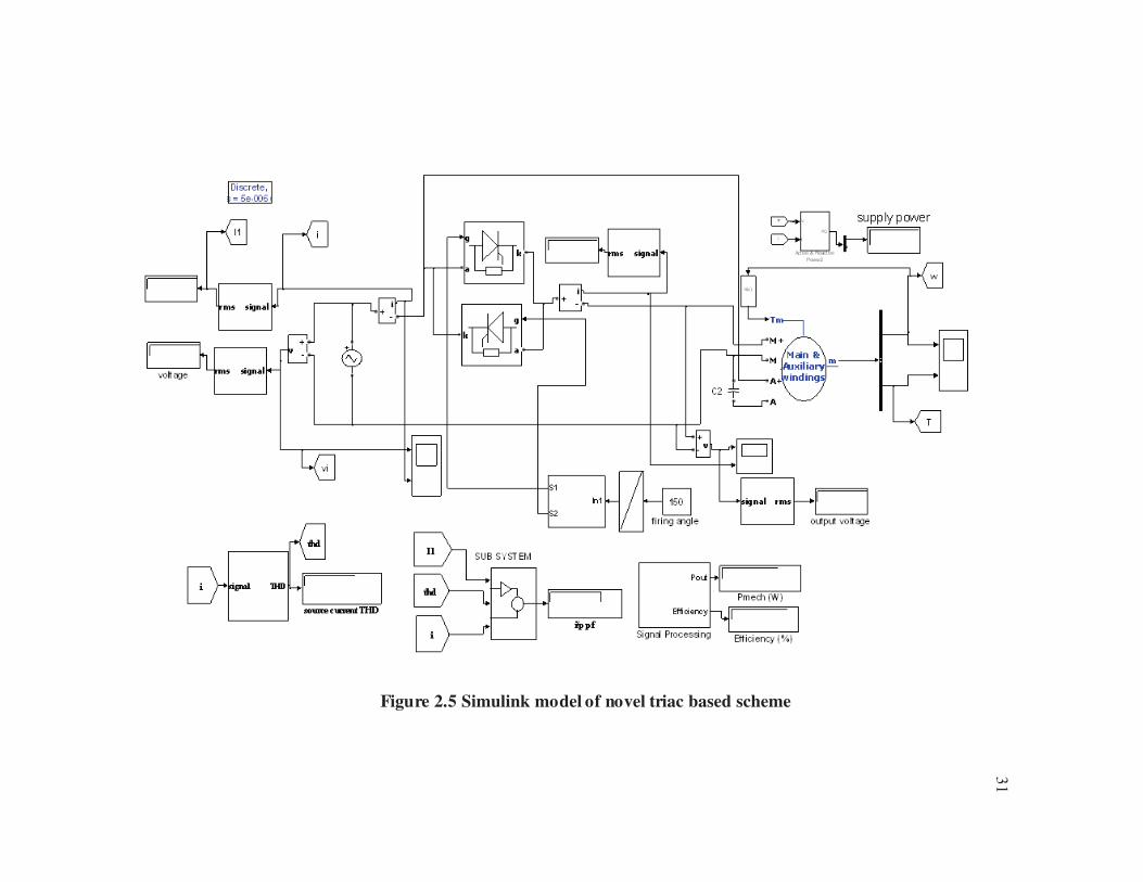
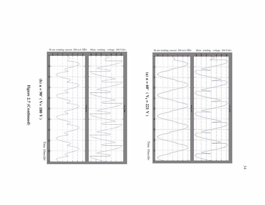
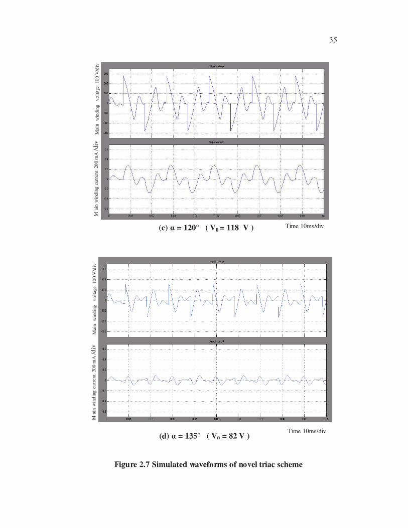
2.5 SIMULATION OF TRIAC BASED SCHEMES
The triac based schemes are simulated using MATLAB/simulink as
shown in Figures 2.4 and 2.5. The simulink models consist of two SCRs
connected in anti-parallel to emulate a triac. The on-state resistance and
voltage drop of the SCRs are considered as 0.001 and 0.8V respectively.
The gating signal which is common to both the SCRs is applied
simultaneously to have equal firing angle in both the half cycles of the input
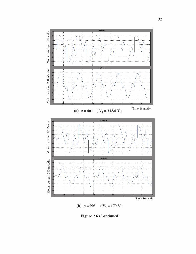
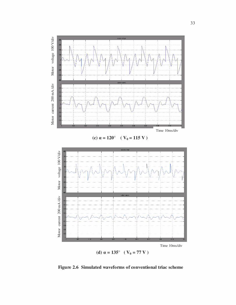
supply.The simulated results of motor current and terminal voltage for several
delay angles( ) are recorded for conventional scheme . In the case of novel
scheme, only main winding voltage and current are recorded as the voltage
and current drawn by the auxiliary winding are sinusoidal. Figures 2.6 and 2.7
show the simulated waveforms of the aforesaid schemes.
30
Figure 2.4 Simulink model of conventional triac based scheme
31
Figure 2.5 Simulink model of novel triac based scheme
32
(b) = 90° ( V0 = 170 V )
Figure 2.6 (Continued)
(a) = 60° ( V0 = 213.5 V )
Moto
r
volt
age
100 V
/div
Moto
r c
urre
nt
200
mA
/d
iv
Time 10ms/div
Moto
r
volt
age
100 V
/div
Moto
r c
urre
nt
200
mA
/d
iv
Time 10ms/div
33
(c) = 120° ( V0 = 115 V )
Moto
r
volt
age
100 V
/div
Moto
r c
urre
nt
200
mA
/d
iv
Time 10ms/div
(d) = 135° ( V0 = 77 V )
Figure 2.6 Simulated waveforms of conventional triac scheme
Moto
r c
urre
nt
200
mA
/d
iv
Time 10ms/div
Moto
r
volt
age
100 V
/div
34
Fig
ure 2
.7 (C
on
tinu
ed)
M ain winding current 200 mA /div Main winding voltage 100 V/div
(a)
= 6
0° ( V
0 = 2
21
V )
Tim
e 10m
s/div
Tim
e 10m
s/div
M ain winding current 200 mA /div
(b)
= 9
0° ( V
= 1
80
V )
Main winding voltage 100 V/div
35
Mai
n
win
din
g
vo
ltag
e 1
00 V
/div
(c) = 120° ( V0 = 118 V )
M a
in w
ind
ing
cur
ren
t 2
00
mA
/div
Time 10ms/div
Time 10ms/div
Mai
n
win
din
g
vo
ltag
e 1
00 V
/div
(d) = 135° ( V0 = 82 V )
M a
in w
ind
ing
cur
ren
t 2
00
mA
/div
Figure 2.7 Simulated waveforms of novel triac scheme
36
Figure 2.8 (Continued)
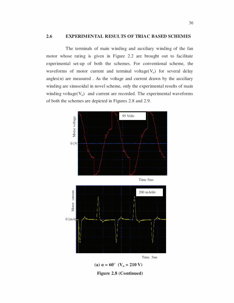
(a) = 60° (Vo = 210 V)
Moto
r c
urre
nt
0 [mA]
Time 5ms
/div
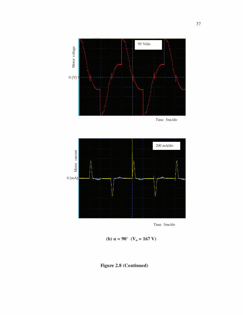
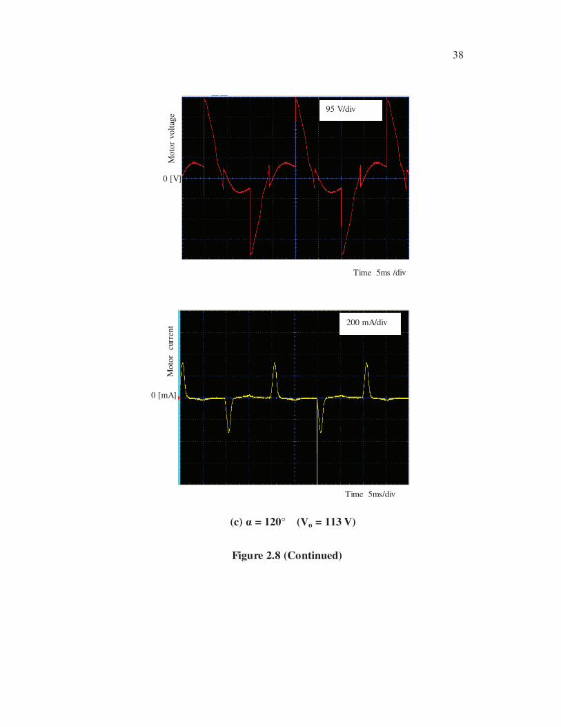
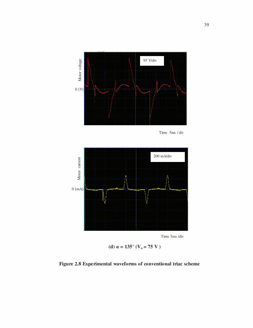
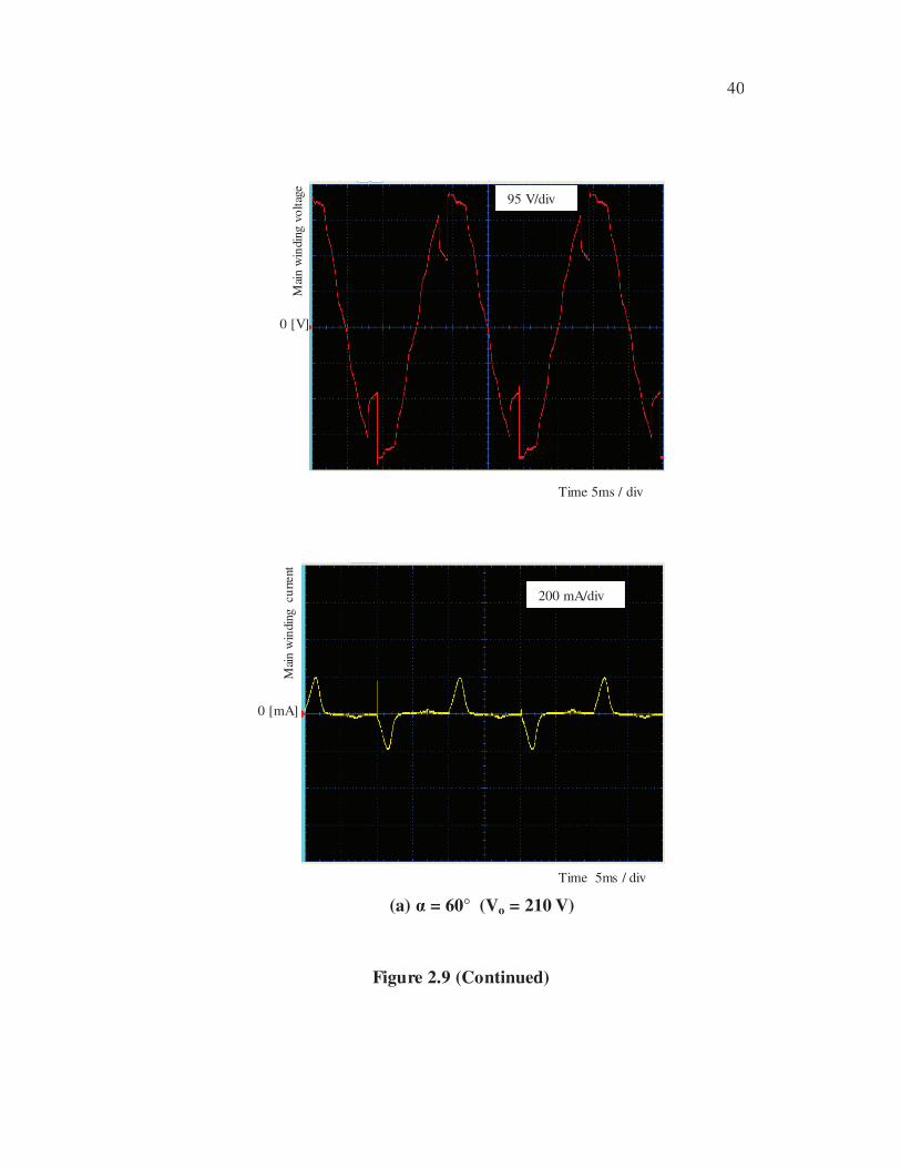
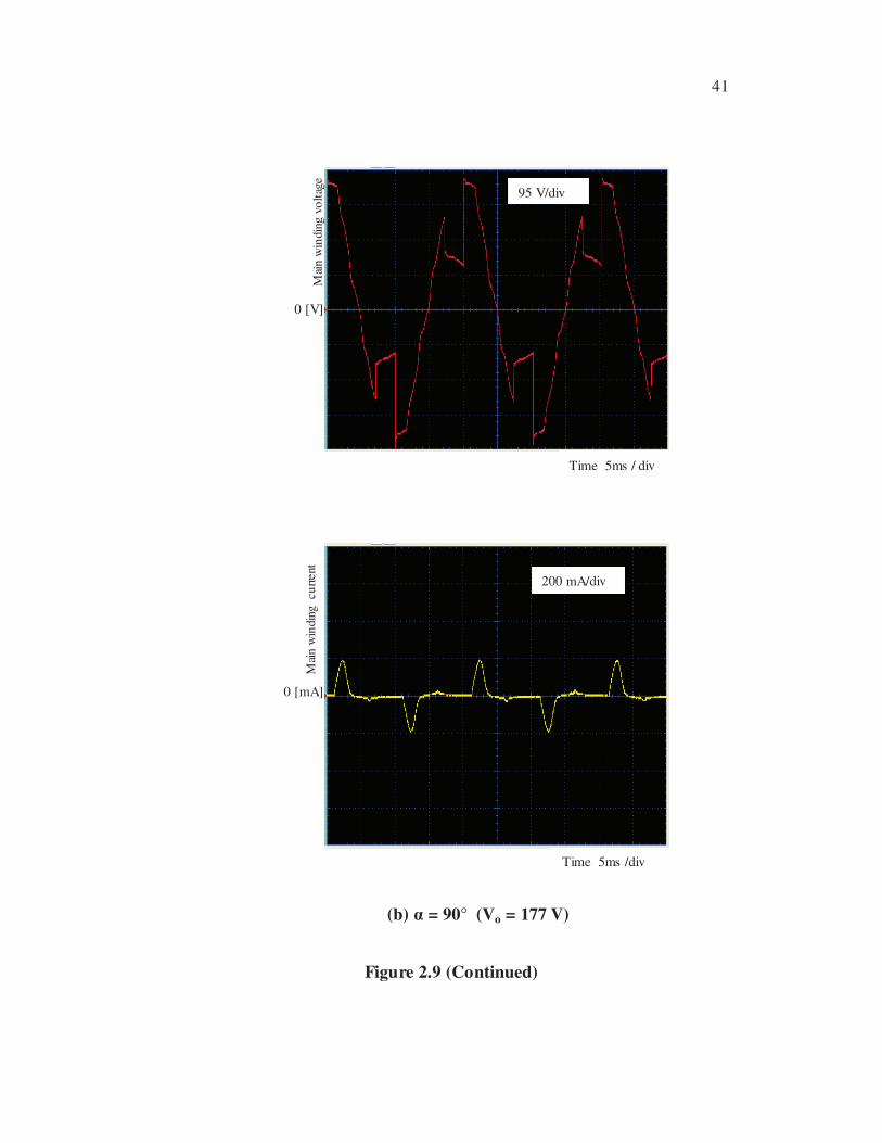
2.6 EXPERIMENTAL RESULTS OF TRIAC BASED SCHEMES
The terminals of main winding and auxiliary winding of the fan
motor whose rating is given in Figure 2.2 are brought out to facilitate
experimental set-up of both the schemes. For conventional scheme, the
waveforms of motor current and terminal voltage(Vo) for several delay
angles( ) are measured . As the voltage and current drawn by the auxiliary
winding are sinusoidal in novel scheme, only the experimental results of main
winding voltage(Vo) and current are recorded. The experimental waveforms
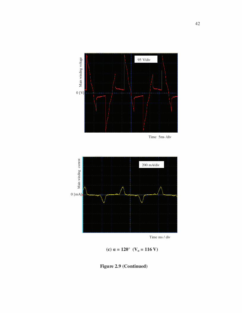
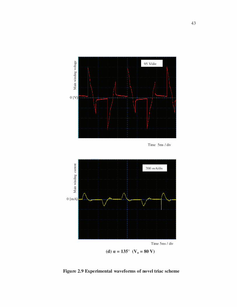
of both the schemes are depicted in Figures 2.8 and 2.9.
0 [V]
Moto
r volt
age 95 V/div
Time 5ms
200 mA/div
37
0 [V]M
oto
r volt
age
95 V/div
Time 5ms/div
Figure 2.8 (Continued)
(b) = 90° (Vo = 167 V)
Time 5ms/div
200 mA/div
Moto
r c
urre
nt
0 [mA]
38
Moto
r c
urre
nt
0 [mA]
200 mA/div
Time 5ms/div
Figure 2.8 (Continued)
0 [V]M
oto
r volt
age
95 V/div
Time 5ms /div
(c) = 120° (Vo = 113 V)
39
(d) = 135° (Vo = 75 V )
Moto
r volt
age
0 [V]
95 V/div
Time 5ms / div
Figure 2.8 Experimental waveforms of conventional triac scheme
Moto
r c
urre
nt 200 mA/div
0 [mA]
Time 5ms /div
40
95 V/div
Mai
n w
indi
ng v
olt
age
0 [V]
Time 5ms / div
(a) = 60° (Vo = 210 V)
Mai
n w
indi
ng c
urr
ent
200 mA/div
0 [mA]
Time 5ms / div
Figure 2.9 (Continued)
41
(b) = 90° (Vo = 177 V)
95 V/div
Mai
n w
indi
ng v
olt
age
0 [V]
Time 5ms / div
0 [mA]
Mai
n w
indi
ng c
urr
ent
200 mA/div
Time 5ms /div
Figure 2.9 (Continued)
42
Mai
n w
indi
ng v
olt
age
0 [V]
95 V/div
Time 5ms /div
(c) = 120° (Vo = 116 V)
200 mA/div
0 [mA]
Mai
n w
indi
ng c
urr
ent
Time ms / div
Figure 2.9 (Continued)
43
(d) = 135° (Vo = 80 V)
0 [V]
95 V/div
Mai
n w
indi
ng v
olt
age
Time 5ms / div
0 [mA]
Mai
n w
indi
ng c
urr
ent
200 mA/div
Time 5ms / div
Figure 2.9 Experimental waveforms of novel triac scheme
44
2.7 DISADVANTAGES
The triac based schemes affect the quality of the input power
supply. Moreover, the presence of substantial amount of lower order
harmonics (at higher values of firing angles) in the voltage available across
the motor or main winding in the case of novel scheme will produce noise and
more heating of the motor.
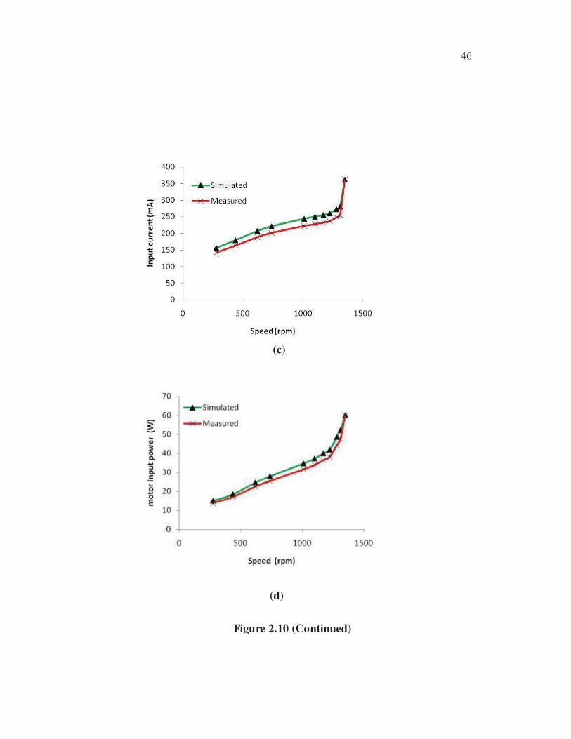
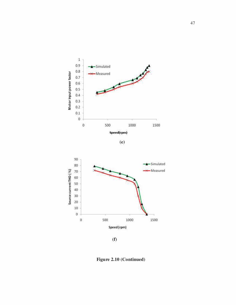
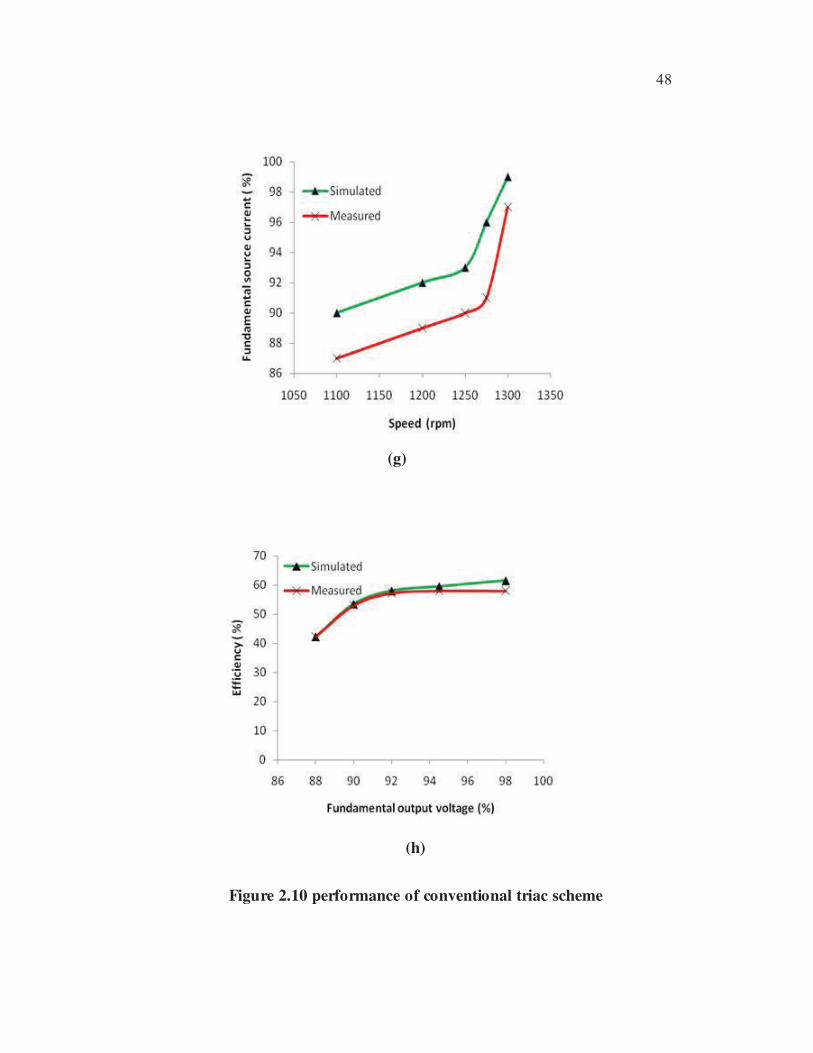
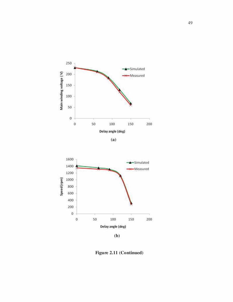
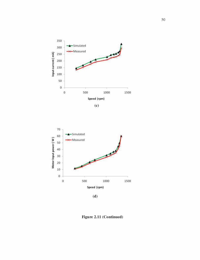
2.8 RESULTS AND DISCUSSION
With the triac based schemes, there is substantial amount of
distortion in the motor terminal voltage and main winding current are
observed. The simulated and experimental waveforms are recorded for
different delay angles as shown in Figures 2.6 to 2.9 to validate the same. It is
found that the simulated results are in close agreement with experimental
results. For validation, certain steady-state characteristics are simulated for
variable-speed/delay angle operation and compared with experimental results
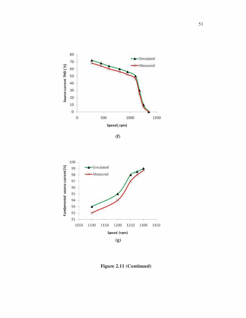
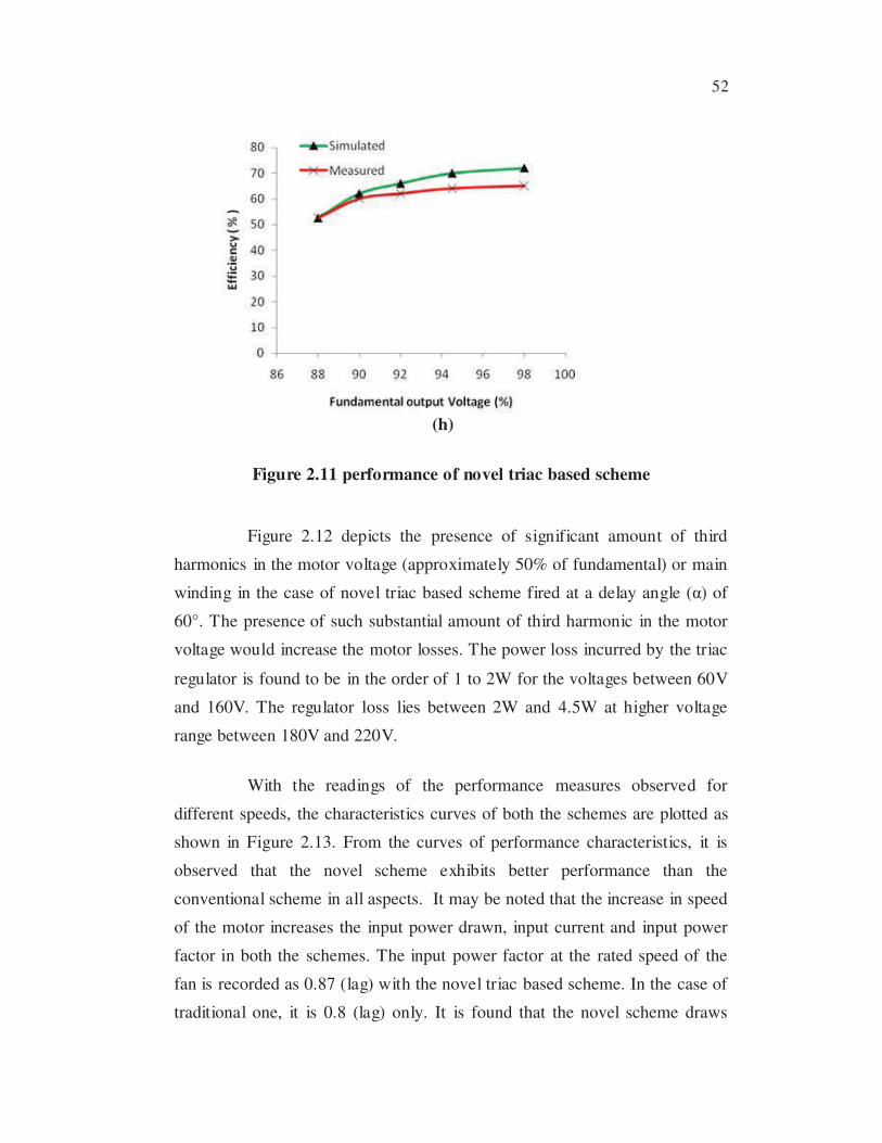
of both the schemes as shown in Figures 2.10 and 2.11. These characteristics
include motor voltage (rms/total), speed, input current (rms/total), input
power drawn from the supply(rms/total), motor input power factor (total),
total harmonic distortion of source current (THD), percentage of fundamental
component in the input current supplied and efficiency. It is observed that
increase in delay angle decreases the motor voltage and speed in both the
cases. Increase in speed increases the input current, input power drawn from
the supply and input power factor as shown in Figures 2.10 (c) to 2.10 (e), and
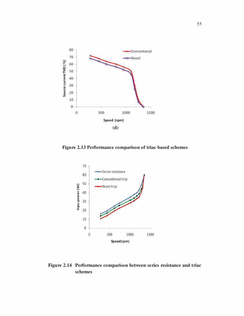
2.11 (c) to 2.11 (e). Figures 2.10 (f) and 2.11(f) show that the THD of source
is very low at higher speeds. The fundamental component of the source
current is higher at higher speeds and it is illustrated in Figures 2.10 (g) and
2.11 (g).
45
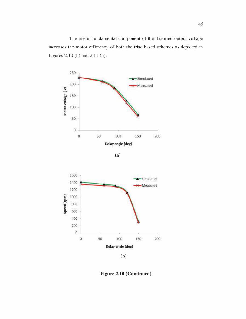
(a)
(b)
The rise in fundamental component of the distorted output voltage
increases the motor efficiency of both the triac based schemes as depicted in
Figures 2.10 (h) and 2.11 (h).
Figure 2.10 (Continued)
46
(c)
(d)
Figure 2.10 (Continued)
47
(e)
Mo
tor
inp
ut
po
we
r fa
cto
r
Figure 2.10 (Continued)
(f)
48
(h)
Figure 2.10 performance of conventional triac scheme
(g)
49
(a)
(b)
Figure 2.11 (Continued)
50
(c)
(d)
Figure 2.11 (Continued)
51
(f)
(g)
Figure 2.11 (Continued)
52
(h)
Figure 2.11 performance of novel triac based scheme
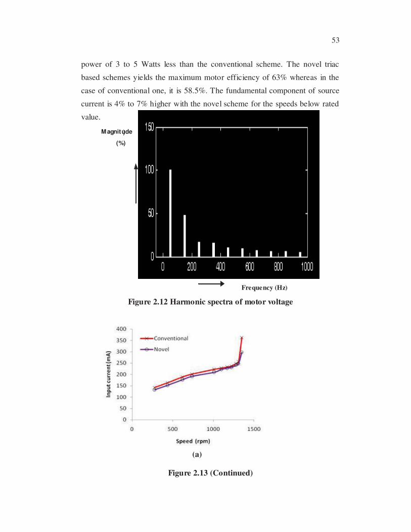
Figure 2.12 depicts the presence of significant amount of third
harmonics in the motor voltage (approximately 50% of fundamental) or main
winding in the case of novel triac based scheme fired at a delay angle ( ) of
60°. The presence of such substantial amount of third harmonic in the motor
voltage would increase the motor losses. The power loss incurred by the triac
regulator is found to be in the order of 1 to 2W for the voltages between 60V
and 160V. The regulator loss lies between 2W and 4.5W at higher voltage
range between 180V and 220V.
With the readings of the performance measures observed for
different speeds, the characteristics curves of both the schemes are plotted as
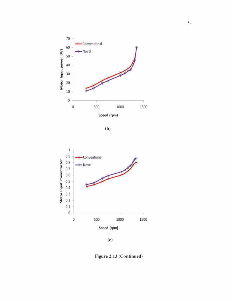
shown in Figure 2.13. From the curves of performance characteristics, it is
observed that the novel scheme exhibits better performance than the
conventional scheme in all aspects. It may be noted that the increase in speed
of the motor increases the input power drawn, input current and input power
factor in both the schemes. The input power factor at the rated speed of the
fan is recorded as 0.87 (lag) with the novel triac based scheme. In the case of
traditional one, it is 0.8 (lag) only. It is found that the novel scheme draws
53
(a)
Frequency (Hz)
M agnitude
(%)
)
power of 3 to 5 Watts less than the conventional scheme. The novel triac
based schemes yields the maximum motor efficiency of 63% whereas in the
case of conventional one, it is 58.5%. The fundamental component of source
current is 4% to 7% higher with the novel scheme for the speeds below rated
value.
Figure 2.12 Harmonic spectra of motor voltage
Figure 2.13 (Continued)
54
(b)
(c)
Figure 2.13 (Continued)
55
(d)
Figure 2.13 Performance comparison of triac based schemes
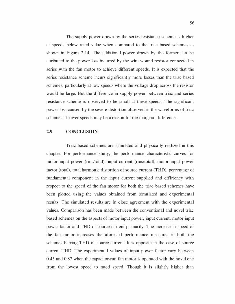
Figure 2.14 Performance comparison between series resistance and triac
schemes
Speed(rpm)
56
The supply power drawn by the series resistance scheme is higher
at speeds below rated value when compared to the triac based schemes as
shown in Figure 2.14. The additional power drawn by the former can be
attributed to the power loss incurred by the wire wound resistor connected in
series with the fan motor to achieve different speeds. It is expected that the
series resistance scheme incurs significantly more losses than the triac based
schemes, particularly at low speeds where the voltage drop across the resistor
would be large. But the difference in supply power between triac and series
resistance scheme is observed to be small at these speeds. The significant
power loss caused by the severe distortion observed in the waveforms of triac
schemes at lower speeds may be a reason for the marginal difference.
2.9 CONCLUSION
Triac based schemes are simulated and physically realized in this
chapter. For performance study, the performance characteristic curves for
motor input power (rms/total), input current (rms/total), motor input power
factor (total), total harmonic distortion of source current (THD), percentage of
fundamental component in the input current supplied and efficiency with
respect to the speed of the fan motor for both the triac based schemes have
been plotted using the values obtained from simulated and experimental
results. The simulated results are in close agreement with the experimental
values. Comparison has been made between the conventional and novel triac
based schemes on the aspects of motor input power, input current, motor input
power factor and THD of source current primarily. The increase in speed of
the fan motor increases the aforesaid performance measures in both the
schemes barring THD of source current. It is opposite in the case of source
current THD. The experimental values of input power factor vary between
0.45 and 0.87 when the capacitor-run fan motor is operated with the novel one
from the lowest speed to rated speed. Though it is slightly higher than
57
traditional scheme, the power factor within this range refers to presence of
substantial amount of harmonics in the main winding current and voltage.
From the harmonic spectra recorded for this scheme, the presence of
significant amount of third harmonics has been found. It is known that the
presence of significant amount of harmonics of this order causes torque ripple
and motor derating due to overheating. The power loss due to overheating can
be attributed to this third harmonics.
The novel triac based scheme has been focused in this chapter as it
offers better performance when compared to conventional scheme. The novel
triac based scheme consumes less power than its conventional counterpart at
speeds below rated value. Owing to this reason, the novel triac based scheme
is considered as an energy efficient scheme. The novel scheme offers
improved power quality unlike the conventional scheme as its THD is
comparatively less. The THD of the novel triac based scheme is 3 to 4% less
than the conventional scheme. Also, the presence of fundamental component
of source current is higher with the novel scheme for the speeds below rated
value.
As far as the hardware requirement is concerned, the novel triac
based scheme does not need any additional components except shifting of the
position of the triac from the supply mains to the main winding. The main and
auxiliary winding currents are close to each other at rated voltage with no
triac control. Also, the maximum reverse voltage across the triac in both the
schemes is equal. Hence, the triac ratings will remain the same for both the
conventional and novel triac based schemes.
It is ascertained that the power consumption of series resistance
scheme is comparatively higher. It is even more than conventional triac based
scheme.