Embed Size (px)
Citation preview
17
CHAPTER 2
LITERATURE REVIEW
Table of Contents
Chapter - 2. Literature Review
S. No. Name of the Sub-Title Page No. 2.1 Introduction 18
2.2 A brief review of multilevel inverter topologies 18
2.2.1 Neutral point clamped (NPC) topology 20
2.2.2 Flying capacitor (FC) topology 24
2.2.3 Cascade H-bridge (CHB) topology 26
2.2.3.1 Operation of cascade multilevel
Inverter 28
2.3 A brief review of modulation techniques for
multilevel inverter 31
2.3.1 Introduction 31
2.3.2 Classification of modulation techniques 33
2.3.2.1 Multilevel Carrier based Sinusoidal
Pulse Width Modulation 34
2.3.2.2 Space Vector Modulation technique 38
2.3.2.3 Selective Harmonic Elimination technique
2.3.2.4 Space Vector Control 51
2.4 Research progress in solving SHE equations 52
2.5 Objective of research 58
2.6 Methodology of Research 59
2.7 Thesis organization 61
18
LITERATURE REVIEW
2.1 INTRODUCTION
This chapter briefly discusses the development of non linear
transcendental Selective Harmonic Elimination (SHE) equation
problem in control of multilevel inverter with an objective of
controlling the chosen multilevel inverter configuration during whole
range of modulation index from 0 to 1 with less %THD which complies
with IEEE 519-1992 harmonic guidelines and also with less switching
losses. Commercially existing topologies of multilevel inverters and
modulation strategy for the control of multilevel inverters are briefly
reviewed. It also reviewed the research progress of various techniques
for solving non linear transcendental SHE equation problem. This
chapter also presents the objective of research, research methodology
and the thesis organization.
2.2 A BRIEF REVIEW OF MULTILEVEL INVERTER TOPOLOGIES
Now-a-days, power requirements of modern industries have
reached to megawatt level. In particular, high-power medium voltage
drives requires power in megawatt range and is usually connected to
the medium voltage network. It is troublesome to connect a single
power semiconductor switch directly to medium voltage grid (2.3kV,
3.3kV, 4.16kV or 6.9 kV). For this reasons, multilevel inverter have
emerged as a cost effective solution for high voltage and high power
applications including power quality and motor drive problems [26].
As a cost effective solution, multilevel converter not only achieves
19
higher voltage and current ratings, but also enables the use of low
power application in renewable energy sources.
These converters are suitable in high voltage and high power
applications due to their ability to synthesize higher voltages with a
limited maximum device rating, less harmonic distortion, producing of
smaller common-mode voltage (CM), less electromagnetic compatibility
(EMC) problems and attain higher voltage with a limited maximum
device rating.
At present, multilevel inverters are extensively used in various
applications such as HVDC transmission [27], distribution generation
systems[28], medium voltage motor drives[29], Flexible AC
Transmission System (FACTS) [30], traction drive systems [31], var
compensation and stability enhancement [32], active filtering [33],
chemical, liquefied natural gas (LNG) plants, marine propulsion [34],
electric vehicle systems (EVS)[35], hybrid electric vehicle
systems(HEV)[36] and adjustable speed drives [ASD][37].
The range of the output power is a very important and evident
limitation of two-level inverter. However, this problem can be
overcome by introducing the concept of multilevel converters in 1975
[38]. The concept of multilevel began with the three-level converter
which is often known as neutral-point converter (NPC) [39]. The word
“converter” refers to the power flow in both the directions i.e. from ac
to dc called as “rectifier” and from dc to ac called as “inverter”. The
20
word “multilevel inverter” refers to using a multilevel converter in the
inverting mode of operation.
In order to meet the challenges such as high dv/dt causing
voltage doubling effect in motor output voltage waveform, %THD to
comply with IEEE 519-1992 harmonic guidelines, high
electromagnetic interference (EMI), high common-mode voltages and
requirements of synthesizing higher voltages for modern industrial
applications have subsequently led the development of various
inverter topologies [40]-[42]. The commercially existing inverter
topologies are neutral point clamped (NPC) inverter, flying capacitor
(FC) and cascaded H-bridge (CHB) inverter topologies and are briefly
reviewed in next section.
2.2.1 Neutral-Point Clamped (NPC) or Diode-Clamped Topology
One of the traditionally accepted and widely used topology for
various industrial and power sector applications is neutral point
converter which was proposed by Nabae, Takahashi and Akagi in
1981[39]. As the two-level inverter has the drawback of achieving
higher power levels with the available GTOs of 4.5kV voltage rating at
that time, for traction applications, three-level inverter configuration
was developed to meet the requirement of high voltage dc operation in
traction application in Austrian railways [43]-[46]. Three-level neutral
point converter often called as three-level diode-clamped inverter has
found wide range application because of the advantages such as
higher power handling capability, less dv/dt and less %THD when
21
compared to conventional two-level inverter. Later, direct extensions of
the original NPC for higher number of levels are presented by several
researchers in 1990s and presented experimental results for the
applications such as variable motor drives, static var compensation
and medium voltage systems interconnections [44]-[48].
The diode-clamped multilevel inverter employs clamping diodes
and cascaded dc capacitors to produce ac voltage waveforms with
multiple levels. However, as the number of levels has increased the
number of clamping diodes, switching devices and dc capacitors also
increases, thus the circuit configuration becomes more complicated.
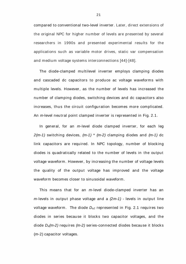
An m-level neutral point clamped inverter is represented in Fig. 2.1.
In general, for an m-level diode clamped inverter, for each leg
2(m-1) switching devices, (m-1) * (m-2) clamping diodes and (m-1) dc
link capacitors are required. In NPC topology, number of blocking
diodes is quadratically related to the number of levels in the output
voltage waveform. However, by increasing the number of voltage levels
the quality of the output voltage has improved and the voltage
waveform becomes closer to sinusoidal waveform.
This means that for an m-level diode-clamped inverter has an
m-levels in output phase voltage and a (2m-1) - levels in output line
voltage waveform. The diode Da2 represented in Fig. 2.1 requires two
diodes in series because it blocks two capacitor voltages, and the
diode Da(m-2) requires (m-2) series-connected diodes because it blocks
(m-2) capacitor voltages.
22
Generally, the voltage across each capacitor for an m-level diode
clamped inverter at steady state is Vdc/(m-1), where Vdc is dc bus
voltage. Though, switching devices in NPC topology are required to
block only a voltage level of Vdc but the clamping diodes require
different ratings to block the reverse voltage. As the number of levels
has increased the capacitor voltage balancing becomes a major
problem.
In this topology, conduction periods of the switching devices are
different. These unequal conduction periods requires different current
ratings of the switching devices. This process leads to some of the
switching devices to be hot, while others stay cooler at the same time.
Fig: 2.1 An m-level Neutral Point Clamped inverter topology

23
This will results in more losses in stressed device which limits the
switching frequency and output power of the converter, thus circuit
design also becomes complicated.
This topology also suffers the disadvantage of unequal load
distribution among the semiconductor switches particularly, when the
inverter runs under pulse width modulation (PWM) technique, the
reverse recovery of the clamping diodes is also a major design
challenge [35, 49]. Though, the operation of NPC topology is simple
and straightforward but as the number of inverter levels increases,
number of devices increases. Hence, design and implementation
becomes so complicated for higher number of levels. The main
advantages and disadvantages are listed below [15,26,40]
Advantages
1) All phases share a common dc bus voltage which minimizes
capacitance requirements of the converter
2) As a group, capacitors can be pre-charged
3) Converter efficiency is high, if it operates at fundamental
switching frequency
4) Simple in control
Disadvantages
1) Since, the number of clamping diodes required is
quadratically related to the number of levels, which results
more complications in design as the number of levels
24
increases
2) Different current ratings of the switching devices are
required due to the difference in conduction periods
3) Possibility of deviation of neutral point voltage
2.2.2 Flying Capacitor(FC) Topology
The Flying capacitor alternatively known as capacitor clamped
inverter topology which was proposed by Meynard and Foch in 1992
[50]. This inverter topology is similar to that of the NPC topology
except the usage of clamping diodes. This topology inverter uses
capacitors instead of clamping diodes. Flying capacitor MLI has
capacitors on dc side and connected like ladder structure, where the
voltage across each capacitor differs from that of the next capacitor.
The number of levels in the output voltage waveform is nothing but
the voltage increment between two adjacent capacitor legs. One
important advantage of the flying-capacitor topology is that it has
phase redundancies for inner voltage levels; in other words, two or
more valid switch combinations are possible to synthesize an output
voltage where as diode clamped inverter has only line-line
redundancies [51].
Choice of specific capacitors for charging and discharging to
incorporate in the control system for balancing the voltages across the
various levels is possible due to the feature of redundancy.
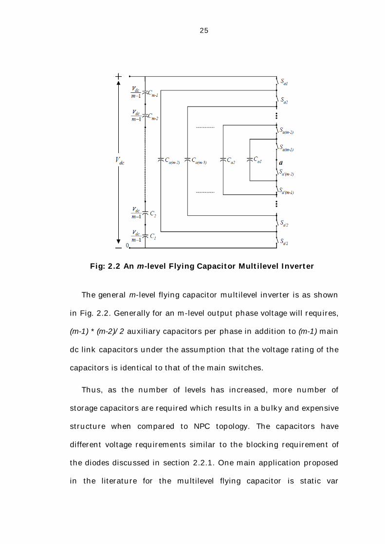
25
The general m-level flying capacitor multilevel inverter is as shown
in Fig. 2.2. Generally for an m-level output phase voltage will requires,
(m-1) * (m-2)/2 auxiliary capacitors per phase in addition to (m-1) main
dc link capacitors under the assumption that the voltage rating of the
capacitors is identical to that of the main switches.
Thus, as the number of levels has increased, more number of
storage capacitors are required which results in a bulky and expensive
structure when compared to NPC topology. The capacitors have
different voltage requirements similar to the blocking requirement of
the diodes discussed in section 2.2.1. One main application proposed
in the literature for the multilevel flying capacitor is static var
Fig: 2.2 An m-level Flying Capacitor Multilevel Inverter

26
generation [15, 40]. The main advantages and disadvantages of FC
topology are listed below [15, 40]:
Advantages
1) Because of flexible phase redundancy, balancing the voltage
levels of the capacitors is possible
2) The large number of capacitors enables the inverter to ride
through short duration outages and deep voltage sags
3) Real and reactive power flows can be controlled
Disadvantages
1) Due to the requirement of more numbers of capacitors
results in bulky and expensive structure than the clamping
diodes used in the diode-clamped multilevel inverter
2) Complex control is required to maintain the capacitors
voltage balance
3) Inverter control is complicated for higher number of levels
4) Packaging is difficult for higher number of levels increases
2.2.3 Cascaded H-bridge (CHB) Topology
The concept of series H-bridge inverter was first proposed by R. H.
Baker and L. H. Banister in 1975 [38]. In order to overcome the
drawbacks of NPC and FC topologies such as extra clamping diodes
and capacitors, Marchesoni.M.,et.al [52] have proposed Cascaded H-
Bridge Inverter. The basic idea of connecting single-phase H-Bridge
27
inverters in cascade with multiple isolated dc supplies to realize
multilevel waveforms was first introduced in 1990 for plasma
stabilization. This modular structure has been subsequently extended
for three-phase applications, such as reactive power compensation by
Peng F.Z., et.al [45]. It was fully realized by the remarkable work of
two researches, Lai and Peng and successfully addressed the
problems of NPC and FC topologies and patented their work in
1997[40]. Since then, the cascaded H-bridge multilevel inverters
(CHBMLI) have drawn significance attention in various applications
because of the attractive features such as [40,53]:
1) Ability to reach higher output voltage and power levels
2) Capable of reaching medium output voltage levels using lower
rating switching components
3) Repairing and replacement of faulty module is easy because of
its high degree of modularity
4) Selecting an appropriate control strategy in the case of fault
conditions can bypass the fault module and can ensure
continuous current to the load, bringing an almost continuous
over all availability
5) Ability to synthesize output voltage waveform with lesser value
of total harmonic distortion (%THD)
These features listed above have made cascaded multilevel
inverters very attractive for high power medium voltage drives and
utility applications [37]. Because of its isolated dc sources, Cascaded

28
inverters are ideal for connecting renewable energy sources with an ac
grid, which is the case in applications such as photovoltaics or fuel
cells. The cascade inverter is also used in regenerative-type motor
drive applications, hybrid electric vehicles, fuel cell based vehicles,
main traction drive in electric vehicles and interfacing with renewable
energy sources [54-56].
Peng has demonstrated a prototype multilevel cascaded static var
generator connected in parallel with the electrical system that could
supply or draw reactive power from an electrical system [46, 57] and
there by either regulate the power factor of the current drawn from the
source or the bus voltage of the electrical system. Later, Peng [45] and
Joos [48] again proved that a cascade inverter can be directly
connected in series with the electrical system for static var
compensation.
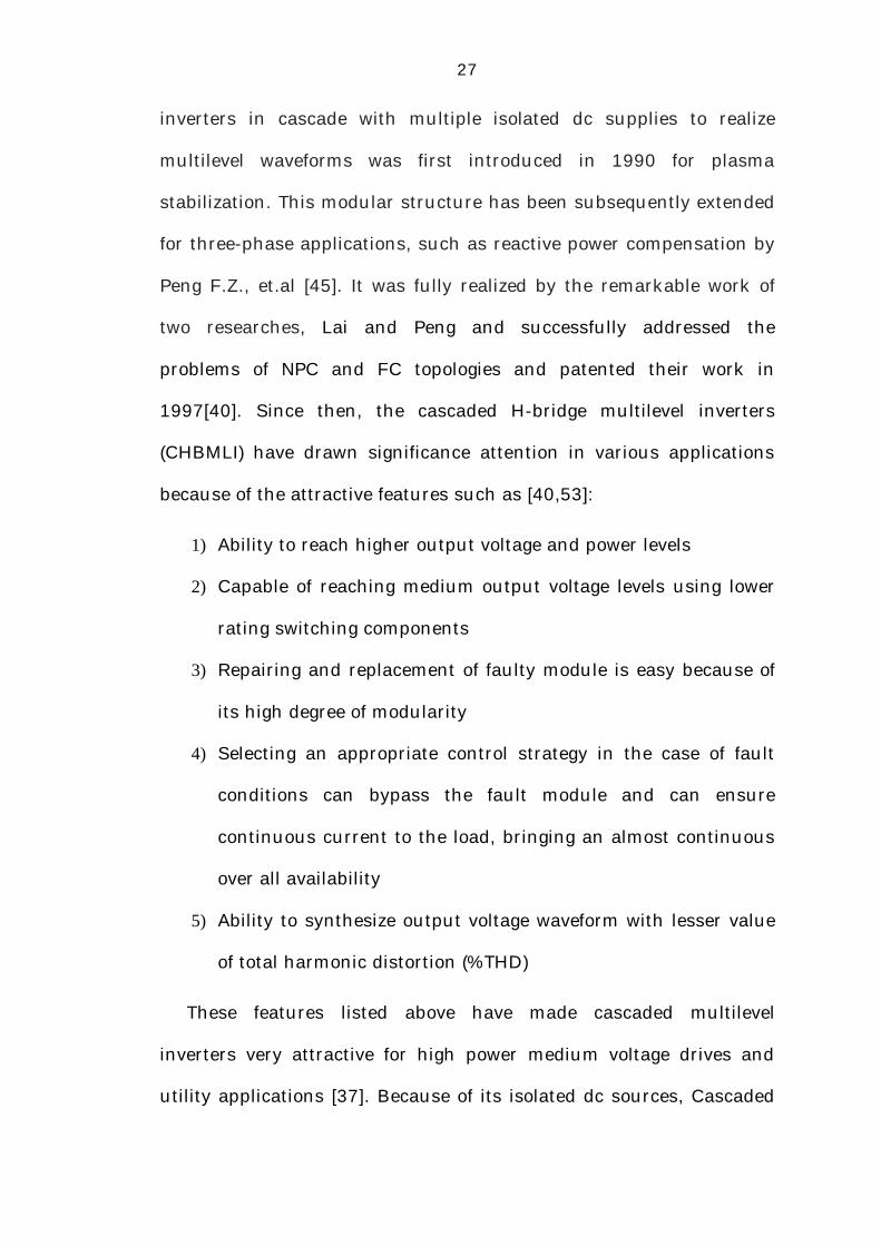
2.2.3.1. Operation of Cascaded Multilevel Inverter
In general, an m-level CHB multilevel inverter consists of 2*(m-1)
power semiconductor switches and (m-1)/2 single-phase H-bridge cells
which are connected in cascade and each bridge has a separate dc
source (SDCS) of value Vdc as shown in Fig. 2.3. This multilevel
inverter can generate almost sinusoidal voltage waveform with only
one time switching per cycle which results in less switching losses.
Moreover, as the number of levels increases total harmonic distortion
decreases but control complexity increases. For a CHB inverter which
29
has “S” number of H-bridge cells then the number of output levels in
output phase waveform is given by (2S+1).
Each inverter can generate three different voltage outputs, +Vdc, 0
and –Vdc by connecting the dc source to the ac output by different
combinations of the four switches such as S1, S2, S3, and S4
repectively. When S1 and S4 switches are turned on +Vdc is obtained,
where as –Vdc can be obtained by turning on switches S2 and S3. Zero
output voltage is obtained by turning on S1 and S2 or S3 and S4.
Fig: 2.3 Single-phase structure of a multilevel Cascaded H-bridge Inverter
30
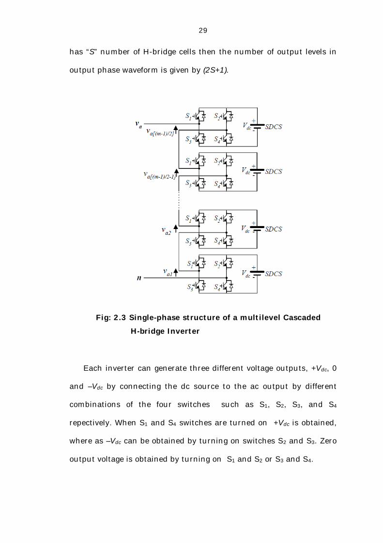
The ac outputs of each of the different full-bridge inverter levels
are connected in series such that the synthesized voltage waveform is
the sum of the inverter outputs. Per phase voltage waveform for an
11-level cascaded H-bridge inverter is shown in Fig.2.4.
For an eleven-level inverter which contains five separate sources,
the per phase voltage is given by
푉 = 푉 + 푉 + 푉 + 푉 + 푉 (2.1)
Thus, staircase waveform is obtained from the CHB multilevel
inverter which can be nearly sinusoidal as the number of levels has
increased, even without using filters. For a three-phase system, the
output voltage of three single-phase cascaded converters can be
connected in either wye (Y) or delta (Δ) configurations.
Fig: 2.4 Output phase voltage waveform of an 11-level CHB inverter with five separate dc sources.
31
In addition to the attractive features mentioned here, the cascade
H-bridge multilevel inverter topology has following limitations [40, 53].
Limitations
1) Because of the requirement of separate isolated H-bridges. This
will limit its application to the products that already have
multiple SDCSs readily available
2) As the number of levels increases, more number of switching
devices are required in this configuration. This requirement
further increases in three-phase configuration.
2.3 A BRIEF REVIEW OF MODULATION TECHNIQUES FOR MULTILEVEL INVERTERS
2.3.1 Introduction
Generally, the semiconductor devices present in the power
converters operate in the “switched mode”, which means in order to
control the power flow in the converter, the switches alternate between
“ON and OFF” states. The switches are always in either one of the two
states - turn off (no current flows), or turn on (saturated with only a
small voltage drop across the switch). Any operation in the linear
region, other than for the unavoidable transition from conducting to
non-conducting, incurs an undesirable loss of efficiency and high
power dissipation in semiconductor switching devices.
Usually, the switched component is attenuated and the desired dc
or low frequency ac component is retained. This process is called
32
Pulse Width Modulation (PWM), since the desired average value is
controlled by modulating the width of the pulses. However, outputs of
these converters may contain different frequency components in
addition to the desired fundamental frequency component. Such
frequency components are undesired in the ac outputs and create
operational imperfections at various levels.
Hence, employing suitable modulation strategies to control MLI
with less %THD in output voltage waveform over wide ranges of
loading conditions with high converter efficiency have been a topic for
intensive research.
Main objectives of modulation strategy are as follows:
1. Capable of operating wide range of modulation index, preferably
from 0 to 1
2. Less switching loss with improved overall converter efficiency
3. Less Total Harmonic Distortion (%THD) in output voltage which
comply with IEEE 519-1992 harmonic guidelines
4. Obtaining high magnitude of the output fundamental frequency
component
5. Easy for implementation for practical applications
6. Computational burden and time should be less
Due to the continuous advancements in solid-state technology,
latest computational techniques, micro-processor technology, dSPACE
technology, digital signal processors and FPGA technology, even the
33
modulation techniques that require complex computations have
become practically implementable.
However, for the converters used in high power applications,
%THD, switching losses, switching capabilities and converter
efficiency are the critical issues that must be taken into account in
performance evaluation.
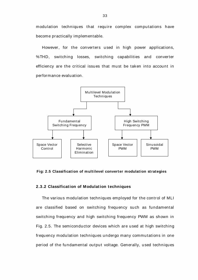
Fig: 2.5 Classification of multilevel converter modulation strategies
2.3.2 Classification of Modulation techniques
The various modulation techniques employed for the control of MLI
are classified based on switching frequency such as fundamental
switching frequency and high switching frequency PWM as shown in
Fig. 2.5. The semiconductor devices which are used at high switching
frequency modulation techniques undergo many commutations in one
period of the fundamental output voltage. Generally, used techniques
Multilevel Modulation Techniques
Fundamental Switching Frequency
High Switching Frequency PWM
Space Vector Control
Selective Harmonic
Elimination
Space Vector PWM
Sinusoidal PWM
34
under this category are sinusoidal PWM and space vector PWM.
The power semiconductor devices used at fundamental switching
frequency under goes one or two commutations during one cycle of
output voltage, generating a stair case waveform. Popular techniques
under this category are selective harmonic elimination (SHE) and
space vector control (SVC) [26,58,59]. The brief review of various
modulation techniques are presented in this section.
2.3.2.1 Multilevel Carrier based Sinusoidal Pulse Width Modulation
Based on traditional sinusoidal pulse width modulation with
triangular carriers, several multilevel carrier based pulse width
modulation techniques have been proposed to reduce %THD in output
voltage. Carrier based sinusoidal pulse width modulation techniques
which are employed in control CHB multilevel inverters can be
generally classified into two categories: phase-shifted and level-shifted
carrier based pulse width modulation techniques.
Level-shifted carrier based PWM (LSCPWM) technique is widely
accepted control technique for neutral point clamped inverter also can
be used to control cascaded multilevel inverters. This technique has
been applied to a five-level inverter and observed the drawbacks such
as uneven distribution of power among cells and high %THD in output
voltage and current waveforms [60].
On other hand, phase shifted carrier based pulse width modulation
(PSCPWM) technique is commonly used modulation technique for
control of cascaded multilevel inverters because of the following
35
reasons: better harmonic profile of output voltage and current
waveforms, even power distribution among cells and easy to
implement independently [37],[61-63]. These advantages made
PSCPWM technique popular compared to LSCPWM technique to
control CHB multilevel inverters.
Generally, a multilevel inverter with m-level voltage requires (m-1)
triangular carriers. All the carriers have same frequency and same
peak-to-peak amplitude with phase shift. The phase shift (휑 )
between adjacent carrier waves is given by
휑 = (2.2)
The modulating signal is usually a three-phase sinusoidal wave
with adjustable amplitude and frequency. By comparing the
modulated wave (VmA) with the carrier waves gate signals are
generated. The fundamental voltage component in the inverter output
voltage can be controlled by modulation index (MI). Modulation index
is the ratio of maximum voltage value of modulating wave (Vm) to
carrier wave voltage (Vcr).
The modulation index (MI) is usually adjusted by varying Vm by
keeping Vcr fixed.
푀 = (2.3)
Bin Wu has implemented carrier based phase shifted PWM
technique on single-phase CHB 7-level inverter [7] as shown in
Fig. 2.6. In this case six triangular signals are required with 600 phase
36
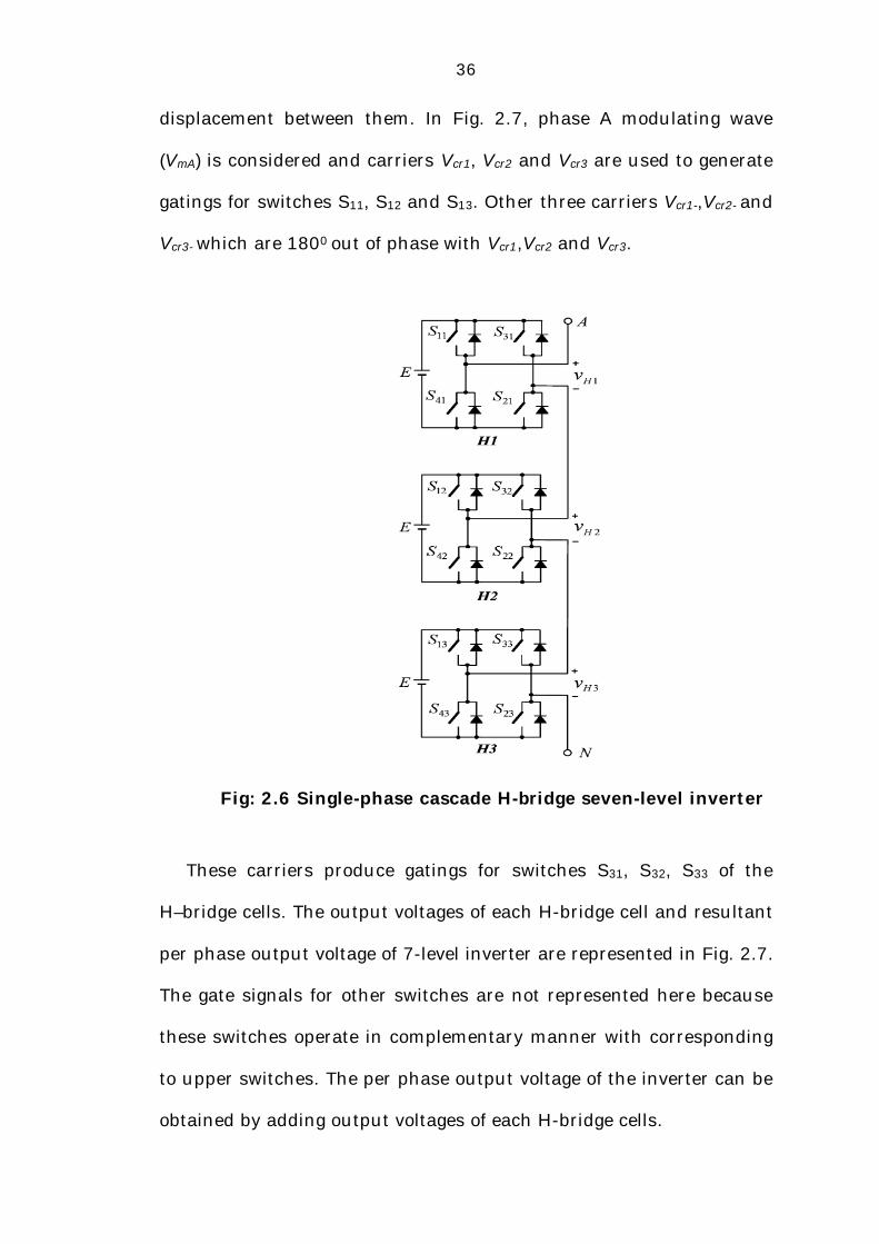
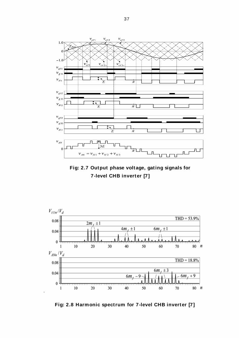
displacement between them. In Fig. 2.7, phase A modulating wave
(VmA) is considered and carriers Vcr1, Vcr2 and Vcr3 are used to generate
gatings for switches S11, S12 and S13. Other three carriers Vcr1-,Vcr2- and
Vcr3- which are 1800 out of phase with Vcr1,Vcr2 and Vcr3.
These carriers produce gatings for switches S31, S32, S33 of the
H–bridge cells. The output voltages of each H-bridge cell and resultant
per phase output voltage of 7-level inverter are represented in Fig. 2.7.
The gate signals for other switches are not represented here because
these switches operate in complementary manner with corresponding
to upper switches. The per phase output voltage of the inverter can be
obtained by adding output voltages of each H-bridge cells.
Fig: 2.6 Single-phase cascade H-bridge seven-level inverter
37
.
Fig: 2.8 Harmonic spectrum for 7-level CHB inverter [7]
Fig: 2.7 Output phase voltage, gating signals for 7-level CHB inverter [7]
38
The seven steps in the per phase output voltage waveform are: +3E,
2E, E, 0, –E, –2E, and –3E. The harmonic spectrum for the voltage
waveforms of H-bridge cell (푉 ) and per phase inverter voltage (푉 ) at
a modulation index of value 1.0 and modulation frequency ( 푚 ) of
value 10 are represented in Fig. 2.7. From Fig. 2.7, it can be seen that
the harmonics in output voltage waveform of H-bridge cell (푉 )
appear as sidebands centered around 2푚 and its multiples such as
4푚 and 6푚 .
It is further observed that the value of %THD in the phase voltage
waveform of CHB 7-level inverter is 18.8% and 푉 is 53.9%.
As mentioned earlier, harmonics in the case the of high switching
frequency modulation techniques appears as sidebands around
carrier frequency produces high %THD which results in trouble some
filtering.
2.3.2.2 Space Vector Modulation Technique (SVM)
Space vector modulation is well established real time modulation
technique and lot of research work have been dedicated to this topic
since decades. Initially, Space vector modulation has been used for
three-phase voltage-source inverters now has been expanded by
application to novel three-phase topologies of multilevel inverters,
matrix converters, current source inverters, resonant three-phase
converters and so on. The attractive features of space vector
modulation are low current ripple, good utilization of dc-link voltage
and easy hardware implementation by advanced digital signal
39
processor. These advantages made space vector modulation suitable
for high-voltage high-power applications [64-69].
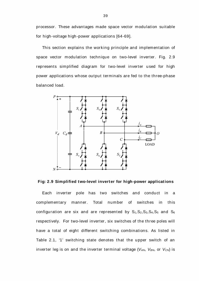
This section explains the working principle and implementation of
space vector modulation technique on two-level inverter. Fig. 2.9
represents simplified diagram for two-level inverter used for high
power applications whose output terminals are fed to the three-phase
balanced load.
Fig: 2.9 Simplified two-level inverter for high-power applications
Each inverter pole has two switches and conduct in a
complementary manner. Total number of switches in this
configuration are six and are represented by S1,S2,S3,S4,S5 and S6
respectively. For two-level inverter, six switches of the three poles will
have a total of eight different switching combinations. As listed in
Table 2.1, ‘1’ switching state denotes that the upper switch of an
inverter leg is on and the inverter terminal voltage (VAN, VBN, or VCN) is
40
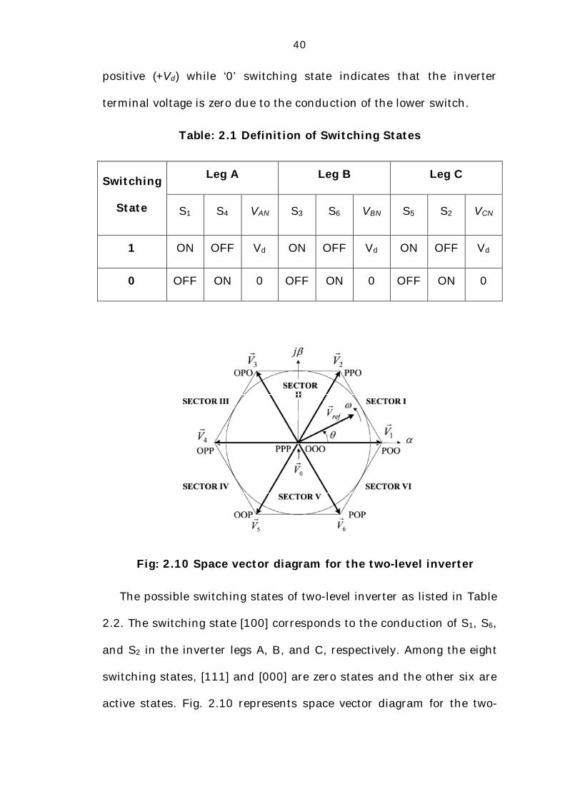
positive (+Vd) while ‘0’ switching state indicates that the inverter
terminal voltage is zero due to the conduction of the lower switch.
Table: 2.1 Definition of Switching States
Switching
State
Leg A Leg B Leg C
S1 S4 VAN S3 S6 VBN S5 S2 VCN
1 ON OFF Vd ON OFF Vd ON OFF Vd
0 OFF ON 0 OFF ON 0 OFF ON 0
Fig: 2.10 Space vector diagram for the two-level inverter
The possible switching states of two-level inverter as listed in Table
2.2. The switching state [100] corresponds to the conduction of S1, S6,
and S2 in the inverter legs A, B, and C, respectively. Among the eight
switching states, [111] and [000] are zero states and the other six are
active states. Fig. 2.10 represents space vector diagram for the two-
41
level inverter, where the zero vector 푉⃗ lies on the centre of hexagon
and six active vectors 푉⃗ to 푉⃗ form a hexagon with equal sectors (I to
VI).
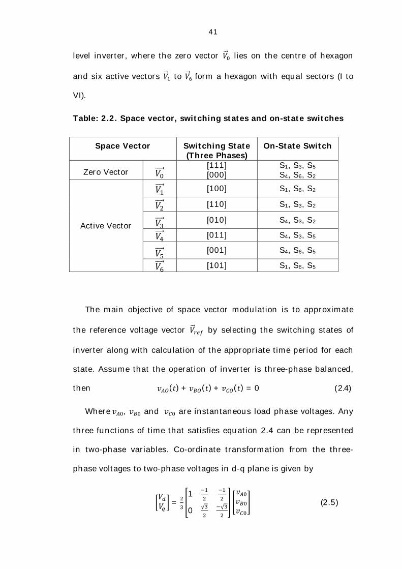
Table: 2.2. Space vector, switching states and on-state switches
Space Vector Switching State (Three Phases)
On-State Switch
Zero Vector 푉⃗ [111] [000]
S1, S3, S5
S4, S6, S2
Active Vector
푉⃗ [100] S1, S6, S2
푉⃗ [110] S1, S3, S2
푉⃗ [010] S4, S3, S2
푉⃗ [011] S4, S3, S5
푉⃗ [001] S4, S6, S5
푉⃗ [101] S1, S6, S5
The main objective of space vector modulation is to approximate
the reference voltage vector 푉⃗ by selecting the switching states of
inverter along with calculation of the appropriate time period for each
state. Assume that the operation of inverter is three-phase balanced,
then 푣 (푡) + 푣 (푡) + 푣 (푡) = 0 (2.4)
Where 푣 , 푣 and 푣 are instantaneous load phase voltages. Any
three functions of time that satisfies equation 2.4 can be represented
in two-phase variables. Co-ordinate transformation from the three-
phase voltages to two-phase voltages in d-q plane is given by
푉푉 =
1
0 √ √
푣푣푣
(2.5)

42
In d-q pane, a space vector can be expressed in terms of the two-
phase voltages as
풗(풕) = 푣 (푡) + 푗푣 (푡) (2.6)
Substituting equation 2.5 in equation 2.6
풗(풕) = 푣 (푡)푒 + 푣 (푡)푒 / + 푣 (푡)푒 / (2.7)
For the switching state [100], the load phase voltages generated are
푣 (푡) = 푉 푣 (푡) = − 푉 and 푣 (푡) = − 푉 (2.8)
Space vector corresponding to switching state [100] can be obtained
by substituting equation 2.8 in 2.7
푉⃗= 푉 푒 (2.9)
Similarly all other active space vector can be derived. In general, all
six active vectors can be derived as
푉⃗= 2
3푉푑푒
푗(푘−1)휋/3,푤ℎ푒푟푒 푘 = 1,2, … . ,6 (2.10)
It is important to note that all the vectors, six active and two zero
vectors are stationary and do not move in space. On other hand, the
reference vector 푉⃗ in Fig. 2.11 rotates in space at an angular
velocity ‘ω’. Where ω = 2πf, ‘f’ is the fundamental frequency of the
inverter output voltage. 푉⃗ can be synthesized by three nearby
stationary vectors in that sector.
43
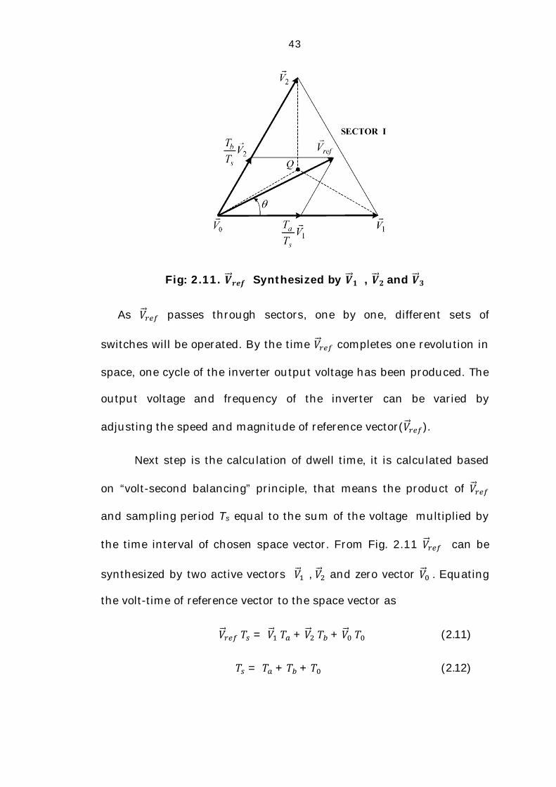
Fig: 2.11. 푽⃗풓풆풇 Synthesized by 푽⃗ퟏ , 푽⃗ퟐ and 푽⃗ퟑ
As 푉⃗ passes through sectors, one by one, different sets of
switches will be operated. By the time 푉⃗ completes one revolution in
space, one cycle of the inverter output voltage has been produced. The
output voltage and frequency of the inverter can be varied by
adjusting the speed and magnitude of reference vector(푉⃗ ).
Next step is the calculation of dwell time, it is calculated based
on “volt-second balancing” principle, that means the product of 푉⃗
and sampling period Ts equal to the sum of the voltage multiplied by
the time interval of chosen space vector. From Fig. 2.11 푉⃗ can be
synthesized by two active vectors 푉⃗ , 푉⃗ and zero vector 푉⃗ . Equating
the volt-time of reference vector to the space vector as
푉⃗ 푇 = 푉⃗ 푇 + 푉⃗ 푇 + 푉⃗ 푇 (2.11)
푇 = 푇 + 푇 + 푇 (2.12)
44
Where Ta, Tb and T0 are dwell time for the vectors
푉⃗, 푉⃗and 푉⃗ respectively. When reference vector present in sector 1,
the dwell times for each vector can be calculated as
푇 = √⃗ sin − 휃 (2.13)
푇 = √⃗
sin휃 (2.14)
푇 = 푇 − 푇 − 푇 (2.15)
For 0 ≤ 휃 ≤ (2.16)
Where ‘θ’ is the angle between reference signal and 푉⃗ and Ts is
switching or sampling period. Equations 2.13 and 2.14 can be
expressed in terms of modulation index (푀 ) as
푇 = 푇 푀 푠푖푛 − 휃 (2.17)
푇 = 푇 푀 푠푖푛휃 (2.18)
Where 푀 = √ ⃗ (2.19)
Next step in space vector modulation is calculation of switching
sequence. In general, switching sequence is selected in such a way to
minimize the device switching frequency. This can be achieved by
switching only one inverter leg at a time during the transition from
one switching state to another. If the reference vector is present in
sector 1, the switching sequence is 푉⃗ , 푉⃗ , 푉⃗ , 푉⃗ , 푉⃗ , 푉⃗ , 푉⃗ and 푉⃗ as
represented in Fig. 2.12.
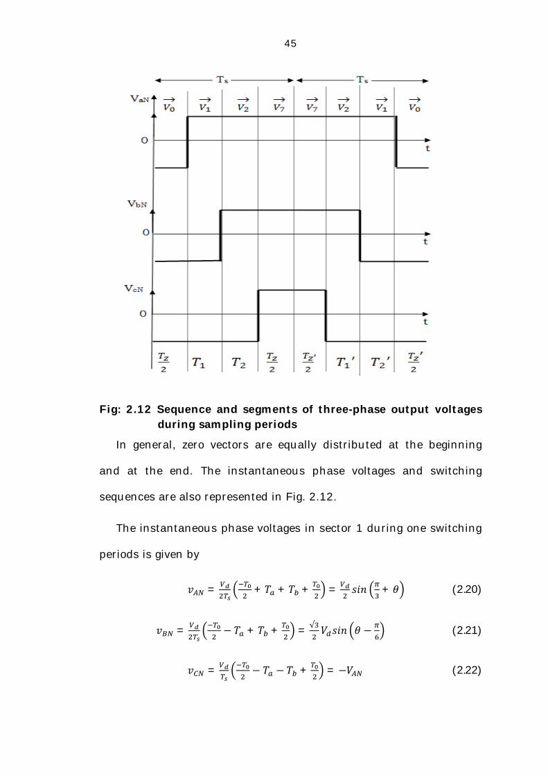
45
Fig: 2.12 Sequence and segments of three-phase output voltages during sampling periods
In general, zero vectors are equally distributed at the beginning
and at the end. The instantaneous phase voltages and switching
sequences are also represented in Fig. 2.12.
The instantaneous phase voltages in sector 1 during one switching
periods is given by
푣 = + 푇 + 푇 + = 푠푖푛 + 휃 (2.20)
푣 = − 푇 + 푇 + = √ 푉 푠푖푛 휃 − (2.21)
푣 = − 푇 − 푇 + = −푉 (2.22)
46
The main disadvantage of space vector modulation technique is,
as the number of levels of the inverter increases, the complexity of
selecting switching states increases which further increases the
computational burden and also it cannot effectively eliminate the
lower order the harmonics [26]. However, Choi [70] was the first
author to implement space vector modulation technique to more than
three- levels for the neutral point clamped inverter topology
2.3.2.3 Selective Harmonic Elimination (SHE) Technique
Selective harmonic elimination technique is one of the traditionally
preferred modulation techniques in control of multilevel inverter since
early 1960s. SHE technique was first introduced by Patel H.S., et al
[71], [72] to eliminate some selected harmonics in half-bridge and full-
bridge inverter output waveforms. SHE can also be called as
preprogrammed pulse width optimum modulation technique which
provides a superior harmonic profile with minimum switching
frequency or switching losses.
SHE offers several advantages such as:
1. Superior harmonic profile with direct control over output voltage
harmonics
2. Operation at fundamental switching frequency which leads to
reduction in device switching losses
3. The ability to leave triplen harmonics uncontrolled to take the
advantage of circuit topology in three-phase systems.

47
These advantages have made SHE technique as a preferred
modulation technique compared to other techniques in applications
such as high-power medium voltage drives [73-74], high voltage direct
current transmission, power quality improvement techniques [26],
distribution generation systems and dual frequency induction heating
[75]. In spite of these advantages, SHE has drawbacks of heavy
computational burden in solving non linear transcendental
trigonometric equations and complicated hardware implementation.
A multilevel inverter can produce a stair case waveform,
synthesized by several dc voltages which are present in cascaded
H-bridge cells. This modulation scheme is based on the calculation of
pre calculated switching angles for multilevel inverters to obtained
required output voltage by minimizing desired order of harmonics.
The principle of operation of SHE is explained in this section by
considering single-phase CHB seven-level inverter as shown in Fig.
2.13. For an m-level inverter which are formed by ‘S’ number of
independent H-bridge cells, consists of ‘S’ number of switching angles
and (S-1) number of harmonics can be eliminated. All the switching
angles considered in SHE technique must be lower than 90°. If the
angles are larger than 90° correct output signal would not be
achievable. From Fig. 2.13, the inverter output phase voltage of
cascade H-bridge 7-level inverter is obtained by the addition of output
voltage of three H-bridge cells
푉 = 푉 + 푉 + 푉 (2.23)
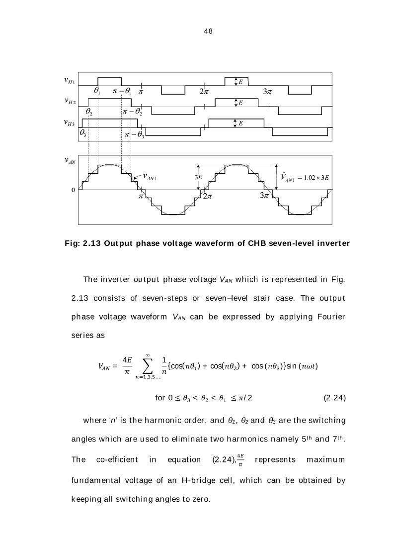
48
The inverter output phase voltage VAN which is represented in Fig.
2.13 consists of seven-steps or seven–level stair case. The output
phase voltage waveform VAN can be expressed by applying Fourier
series as
푉 = 4퐸휋
1푛
∞
, , ….
{cos(푛휃 ) + cos(푛휃 ) + cos (푛휃 )}sin (푛휔푡)
for 0 ≤ 휃 < 휃 < 휃 ≤ 휋/2 (2.24)
where ‘n’ is the harmonic order, and θ1, θ2 and θ3 are the switching
angles which are used to eliminate two harmonics namely 5th and 7th.
The co-efficient in equation (2.24), represents maximum
fundamental voltage of an H-bridge cell, which can be obtained by
keeping all switching angles to zero.
Fig: 2.13 Output phase voltage waveform of CHB seven-level inverter

49
The modulation index (MI), is defined as the ratio of the
fundamental output voltage (V1) to the maximum obtainable
fundamental voltage (V1max)
푀 =
(2.25)
From (2.24), the expression for the fundamental voltage in terms of
switching angles is given by
푉 = (cos(휃 ) + cos(휃 ) + cos (휃 )) (2.26)
Here S =3, so three degrees of freedom, one is used to control the
magnitude of fundamental voltage and other two degrees of freedom
are used to eliminate two harmonics and also provide an adjustable
modulation index (푀 ). Thus, the modulation index for cascade H-
bridge 7-level inverter is defined as
푀 = (2.27)
Thus by combining equations (2.24) and (2.26) for elimination 5th
and 7th order harmonics, the following equations are formulated
cos(7휃 ) + cos(7휃 ) + cos(7휃 ) = 0
cos(5휃 ) + cos(5휃 ) + cos(5휃 ) = 0
cos(휃 ) + cos(휃 ) + cos(휃 ) = 3푀 (2.28)
These equations set (2.28) that are formulated and called as
nonlinear transcendental trigonometric equations that can be solved
by an iterative method such as the Newton-Raphson method.
50
For example, at modulation index of value 0.8, the switching angles
obtained are as follows: θ1= 57.106°, θ2=28.7170, θ3= 11.504°.
The major difficulty for selective harmonic elimination method is to
solve highly non liner transcendental equation set (2.28) for switching
angles. Newton-Raphson method can be used to solve equation (2.28),
but it needs good initial guess, and solutions are not guaranteed.
Therefore, Newton Raphson method is not feasible to solve equations
for large number of switching angles if good initial guesses are not
available.
Compared with other modulation techniques, SHE technique is
simple to implement and has a feature of operating at fundamental
frequency which results in less switching losses with better harmonic
profile in the inverter output voltage waveform. All the switching
angles can be calculated in off-line and stored up in a look-up table to
generate PWM gate drive signals.
In order to overcome the drawbacks such as prolonged
computations, long computational time, convergence into local
minima and providing analytical solutions during the full range of
modulation index from 0 to 1 with an objective of producing less
%THD to comply with IEEE 519-1992 harmonic guidelines has been a
challenging research topic since several decades .
The above mentioned drawbacks are addressed in this work and
validated the simulation results with experimental approach too.
51
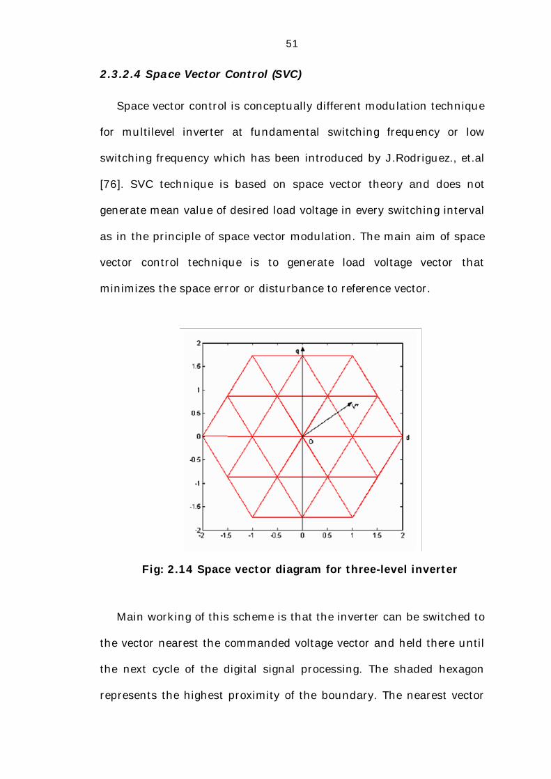
2.3.2.4 Space Vector Control (SVC)
Space vector control is conceptually different modulation technique
for multilevel inverter at fundamental switching frequency or low
switching frequency which has been introduced by J.Rodriguez., et.al
[76]. SVC technique is based on space vector theory and does not
generate mean value of desired load voltage in every switching interval
as in the principle of space vector modulation. The main aim of space
vector control technique is to generate load voltage vector that
minimizes the space error or disturbance to reference vector.
Main working of this scheme is that the inverter can be switched to
the vector nearest the commanded voltage vector and held there until
the next cycle of the digital signal processing. The shaded hexagon
represents the highest proximity of the boundary. The nearest vector
Fig: 2.14 Space vector diagram for three-level inverter
52
to the commanded voltages (v*) is determined according to the
hexagonal regions around each vector because it has highest
proximity to the reference (푉⃗ ). Though SVC technique is simple to
implement but the error in terms of generated vectors with respect to
reference will be more as the number of levels of the inverter
decreases which increases the ripples in the load current waveform.
However, this technique will be more attractive for high number of
levels [26].
2.4 RESEARCH PROGRESS IN SOLVING SHE EQUATIONS
The equations which are formed by SHE technique are highly non
linear transcendental in nature that contains trigonometric terms
which exhibits single, multiple or even no solution for a particular
modulation index. As the number of levels of the inverter increases,
complexity of solving the problem further increases because the
number variables (i.e. switching angles) to obtain feasible solutions
increases. SHE equations are associated with analysis of the problem
are solved by using optimization algorithms rather than elimination
algorithms. However, researchers have proposed several techniques in
literature to solve SHE equations over a range of modulation index
which in turn control the desired MLI with least %THD to comply with
IEEE 519-1992 harmonic guidelines.
H.S.Patel and R.G.Hoft have applied a well-known numerical
iterative approach called Newton-Raphson (NR) method in 1973 to the
SHE equations [71]. NR method needs a good initial guess that should
53
be very close to the exact solution otherwise it results in long tedious
computations. However, the search space for SHE equations set is
unknown providing good initial guess at all times are not possible.
Moreover, this method contains gradient operation, the probability of
convergence at local minimum is more [77].
Sun & Grotstollen in 1992 used predicted initial values [78] and
T.J. Liang et al. in 1997 proposed WALSH functions[79] to solve SHE
equations both these methods require more computational effort to
obtain the feasible solutions. John N.Chiasson et.al in 2003 have
proposed Resultant theory to eliminate fifth and seventh harmonics in
a seven-level inverter [80]. In Resultant theory approach,
transcendental equations characterizing harmonic content can be
converted into an equivalent set of polynomial equations and then
resultant theory method is utilized to find all possible sets of solutions
and the solution set which produces least %THD have been
considered. John N.Chiasson et al. have presented experimental
results in control of three-phase seven-level inverter at the modulation
indices of value 0.5,1.0,1.5,2.0 and 2.5 respectively.
In this approach the targeted harmonics such as 5th and 7th are not
minimized at the modulation indices of value 0.5 and 0.7 and
minimized to a greater extent at the modulation indices of value 1.5,
2.0 and 2.5. Authors have not reported how the resultant theory has
solved the SHE equations set during complete range of standard
modulation index from 0 to 1.
54
Elimination theory proposed by J.N. Chiasson et.al in 2004[81] to
find all possible solutions to the SHE equations set in contrast to the
well known work of Patel and Hoft. This approach has successfully
found the solutions set in between the range of modulation indices
from 0.53 to 0.78 where NR method could not find solution. Authors
have presented the experimental results at the modulation indices of
value 0.7 and 0.5 respectively. Even though the targeted harmonics
are minimized, authors have not tested how the elimination theory
has explored the solution for SHE equations set during complete
range of modulation index from 0 to1.
A unified approach has been proposed by J.N. Chiasson et.al in
2004[82], where non linear transcendental SHE equations for all
possible switching schemes, first converted into a single set of
symmetric polynomial equations and complete set of solutions are
found using the method of resultant from elimination theory.
Experimental results have been presented with an objective of
minimizing fifth and seventh order harmonics in seven-level inverter.
Here, the possible switching schemes for seven-level inverter have
been considered and %THD of each scheme at a particular modulation
index has been observed. Harmonic profile at ‘푚 ’ of values 0.49,
1.39, 1.45, 1.67, 1.84, 1.93 were observed. Where 푚 = .
Though the simulation results validated the experimental results,
unified approach has not presented the solution of SHE equations set
during complete range of modulation index from 0 to 1.
55
As the number of dc sources increases, the degrees of polynomials
are also increases which further increase the computational burden.
In order to address this problem, John.N.Chiasson et.al have
proposed theory of Symmetric Polynomials and Resultants in
2005[83].
The main drawback of elimination theory is as the number of levels
of the inverter increases, the degrees of the polynomial increases. As a
result, one reaches the limitations of the capability of contemporary
software tools (MATHEMATICA or MAPLE) to solve polynomial
equations. Theory of symmetric polynomials can be exploited to which
in turn reduces the computational burden within the capability of
existing computing tools. From computational results, it is observed
that, for ‘푚 ’ in the intervals [2.21,3.66], [3.74,4.23] and at 1.88, 1.89,
the developed algorithm has successfully eliminated desired order of
harmonics such as 5th,7th,11th and 13th.
Further, it is seen that, in the narrow interval of [2.53,2.9] and
[3.05,3.29] feasible solutions have been obtained. Though, theory of
symmetric polynomials and resultants has overcome the drawbacks of
elimination theory like unable to find analytical solution for five
switching angles even after running more than nine hours on a
Pentium III, 1.2MHz processor with 0.5GB of RAM using software tool
like MATHEMATICA. However, the authors have mentioned the
computational difficulty in solving determinants of Sylvester matrices
with dimension 33x33. This computational difficulty further increases
56
with the number of harmonics to be eliminated increases. Vassilios G
et.al in 2008 proposed technique called Function minimization to
solve SHE equations. This technique also suffers the drawback of
prolong computations [84].
All the techniques mentioned above, suffer from long tedious
calculations, prolonged computations and could not find the feasible
solutions during entire range of modulation index from 0 to 1. In order
to overcome the computational difficulty and to find the feasible
solution for SHE equations during entire range of modulation index
from 0 to 1, Stochastic Optimization techniques like Genetic
Algorithms and Particle Swarm Optimization techniques are seemed
to be promising in providing a solution to SHE equations set during
complete range of modulation index from 0 to 1.
Burak Ozpineci et.al have applied Genetic Algorithms to solve non
linear transcendental SHE equations set which involves three and five
switching angles. Experimental validation has been done on both
seven and eleven-level multilevel inverters. From experimental results
on seven-level inverter, it is observed that proposed algorithm could
not find solution in the range [0, 0.5] and at the modulation index of
value 1.061, fifth and seventh order of harmonics are minimized.
Experimental results on 11-level inverter shows that proposed
algorithm could not find solution below modulation indices of value
0.6 and above of value 1.1. Though, the present work reduces the
computational burden but unable to find the feasible solution during
57
complete range of modulation index [85].
Reza Salehi et.al in 2011 have applied Continuous-Genetic
Algorithm to solve SHE equations which are formed by single-phase
cascade H-bridge nine-level inverter. From computational results, it is
observed that, proposed algorithm has successfully solved SHE
equations set during entire range of modulation index from 0 to 1 but
authors have not validated the simulation results with experimental
approach [86].
Basic particle swarm optimization was modified and Modified
Species based Swarm Optimization was proposed by Mehrdad
Tarafdar et al. in 2009. This work presents an effective algorithm to
solve SHE equations set which involves solving of fifteen switching
angles. Experimental results at the modulation index of value 1.0 has
been presented, FFT analysis reveals that order of the harmonics up
to 60, are minimized to a greater extent.
Though, the developed algorithm has successfully eliminated
harmonics at the modulation index of value 1.0, it could not find the
feasible solution in the range of modulation index [0,0.55]. The
authors have not reported the experimental results at various values
of modulation index other than 1.0[77].
58
2.5 OBJECTIVES OF RESEARCH
In literature so far different techniques have been proposed to solve
non linear transcendental SHE equations. Newton-Raphson method
suffers from the drawback of requirement of good initial guess and
could not find the solution during complete range of modulation
index. All the proposed methods after NR method like Predicted initial
values, WALSH functions, Resultant theory, Elimination theory, A
Unified approach, Symmetric Polynomials and Resultants, Function
minimization suffers from drawbacks of prolonged calculations and
tedious computational effort. Though, this problem is effectively
minimized by using stochastic optimization techniques all these
proposed techniques could not find the feasible solution during entire
range of modulation index from 0 to 1.
Further, none of the above authors have presented the
experimental results during the entire range of Modulation index. It is
further observed that, from the literature survey carried out, no
author has presented how both the deterministic and stochastic
algorithms work in solving non linear transcendental SHE equations
which are formed in control of three-phase cascade H-bridge 11-level
inverter. Three phase cascade H-bridge inverter is one of the preferred
topology by high power medium voltage drive manufacturers [7].
Hence this topology has been chosen for analysis.
The main objective of this work is to develop most efficient and
rugged algorithm to obtain the feasible solutions for non linear
59
transcendental trigonometric equations which are formed by SHE
technique with less computational effort and without prolonged
calculations, during complete range of modulation index from 0 to 1,
which in turn controls the chosen multilevel inverter with less %THD
which complies with IEEE 519-1992 harmonic guidelines.
Deterministic method like Newton-Raphson(NR) method, stochastic
methods like Continuous-Genetic Algorithm(C-GA) and Modified
Species based Particle Swarm Optimization(MPSO) techniques have
been applied to solve non linear transcendental SHE equations which
are formed in control of three-phase cascade H-bridge inverter to
explore the potential of deterministic and stochastic algorithms and
comparative analysis have been carried out.
Finally, an efficient robust algorithm which solves the SHE
equations set with less computational effort and time has been
developed and validated the effectiveness of proposed algorithm in real
time too. The results Obtained over major range of modulation index
comply with IEEE 519-1992 harmonic guidelines too.
2.6 METHODOLOGY OF RESEARCH
In the elaboration of the research, one of the preferred inverter
configurations used in high-power medium voltage drives such as
three-phase cascade H-bridge 11-level inverter has been chosen for
analysis. Selective harmonic elimination modulation technique has
been applied to chosen inverter configuration and formulated the
objective function and fitness/cost function. MATLAB programming
60
environment is chosen for developing code for Newton-Raphson,
Continuous-Genetic Algorithm and Modified Species based Particle
Swarm Optimization techniques.
The computed switching angles are considered for control of semi
conductor switching devices in MALTAB simulink model and line to
line output voltage, phase output voltage waveforms are observed.
From FFT analysis, magnitude of harmonics and %THDs are observed
at each modulation index from 0 to 1 in steps of 0.1. The potential of
solving the SHE equations set in deterministic and stochastic
algorithms are explored during complete range of modulation index
from 0 to 1.
A comparative harmonic analysis has been carried out with
simple rugged and efficient algorithm to solve SHE equations set
during complete range from 0 to 1, among all techniques has been
selected. To validate the effectiveness of proposed MPSO technique an
experiment is conducted on low power prototype of three-phase
cascade H-bridge 11-level inverter. FPGA based Xilinx’s SPARTAN 3-A
DSP controller is used to generate gating signals for switching devices
in the hardware circuit. Experiment is repeated at each modulation
index from 0 to 1 in steps of 0.1 and %THDs at each step has been
observed.
61
2.7 THESIS ORGANIZATION
This thesis consists of seven chapters and arranged as follows:
Chapter 1 covers, the introduction to high-power medium voltage
drives, complete explanation of general block diagram, applications in
modern industry, technical challenges in control of MV drives and
various inverter topologies used by MV Drive manufacturers in
present market are briefly discussed.
Chapter 2 discusses literature review on various multilevel inverter
topologies and various modulation control techniques for control of
multilevel inverter such as sinusoidal pulse width modulation, space
vector modulation, space vector control and selective harmonic
elimination techniques are reviewed. It also reviewed the various
techniques to obtain analytical solutions for non linear transcendental
SHE equations.
Chapter 3 In this chapter formation of mathematical models of
switching angles and formation of SHE equations for three-phase CHB
11-level inverter are presented. It also presents the formation of
objective function and fitness or cost function for given optimization
problem.
Chapter 4 presents the coding development for proposed algorithms
such as deterministic methods like Newton-Raphson method,
Stochastic methods like Continuous-Genetic algorithm and Modified
Species based Particle Swarm Optimization techniques. The developed
algorithms are applied to solve SHE equation set and results are
62
presented in chapter 6.
Chapter 5 This chapter elucidates development of hardware circuit for
experimental validation. It further discusses the interfacing of
MATLAB programming part with hardware circuit. FPGA based
Xilinx’s SPARTAN-3A DSP controller for gate pulse generation has
been discussed. The testing of proposed MPSO algorithm and test
results at each modulation index has been presented in chapter 6.
Chapter 6 provides the simulation results of Newton-Raphson,
Continuous-Genetic algorithm and Modified Species based Particle
Swarm Optimization techniques. It also presents the experimental
results of proposed MPSO technique in control of chosen inverter
configuration. Comparative analysis has been carried out from the
obtained simulation and experimental results.
Chapter 7 summarizes the conclusions of research work and
recommendations for further research work have been presented.