Embed Size (px)
Citation preview
Chapter 2
Introduction to Logic Circuits
• Logic functions and circuits
• Boolean algebra
• Synthesis of digital circuits
• Introduction to CAD tools
• Introduction to VHDL
Chapter 2-2
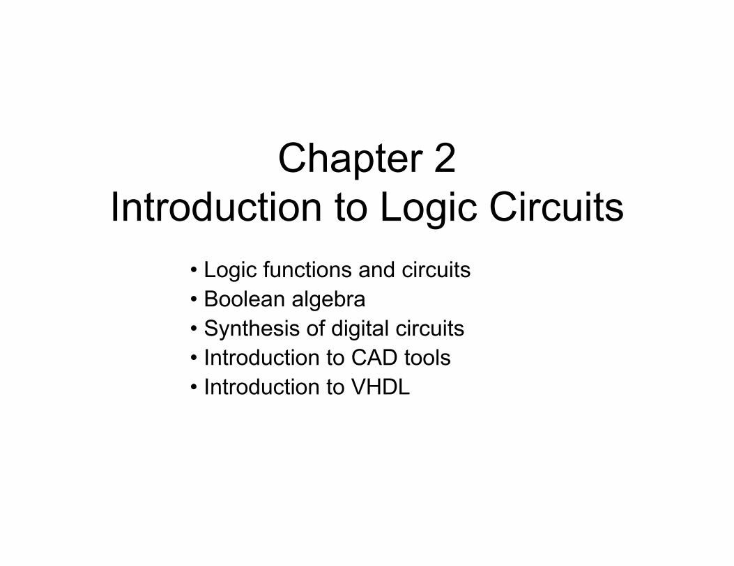
Figure 2.6. A truth table for the AND and OR operations.
Logic functions and Circuits
x1 and x2 are binary variables, that may take on only one of two
Possible values, i.e., 0 or 1
Chapter 2-3
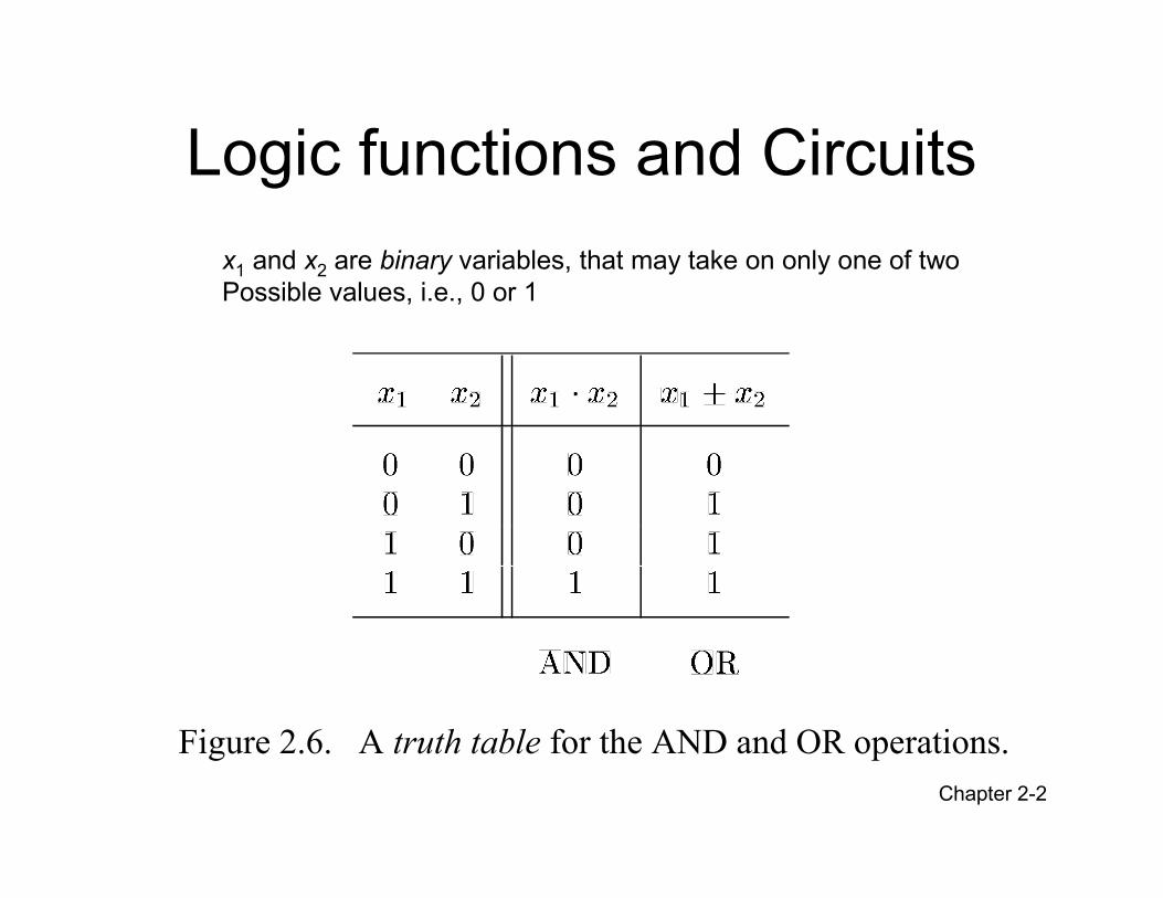
(a) AND gates
(b) OR gates
x x
x 1 x 2
x n
x 1
x 2 … x
n + + +
x 1 x 2
x 1
x 2
+
(c) NOT gate
Figure 2.8. The basic gates.
x 1 x 2
x n
x 1 x 2
x 1
x 2 ⋅ x
1 x 2 … x n ⋅ ⋅ ⋅
Chapter 2-4
x 1
x 2
1 1 0 0 → → →
f
0 0 0 1 → → →
1 1 0 1 → → →
0 0 1 1 → → →
0 1 0 1 → → →
A
B
x 1
x 2
f x 1x 2
, ( )
0
1
0
1
0
0
1
1
1
1
0
1
(b) Truth table
A B
1 0
1 0
0 0
0 1
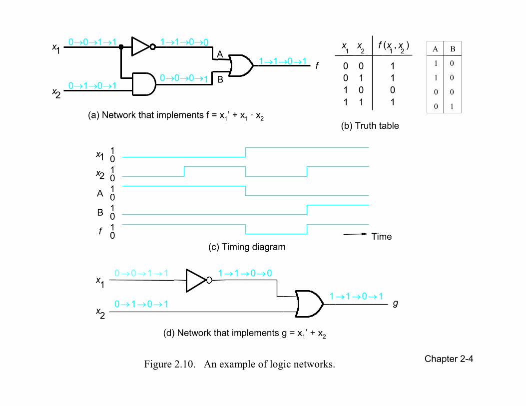
(a) Network that implements f = x1’ + x1 · x2
1 0 1 0 1 0 1 0 1 0
x 1
x 2
A
B
f Time
(c) Timing diagram
1 1 0 0 → → →0 0 1 1 → → →
1 1 0 1 → → →0 1 0 1 → → → g
x 1
x 2
(d) Network that implements g = x1’ + x2
Figure 2.10. An example of logic networks.
Chapter 2-5
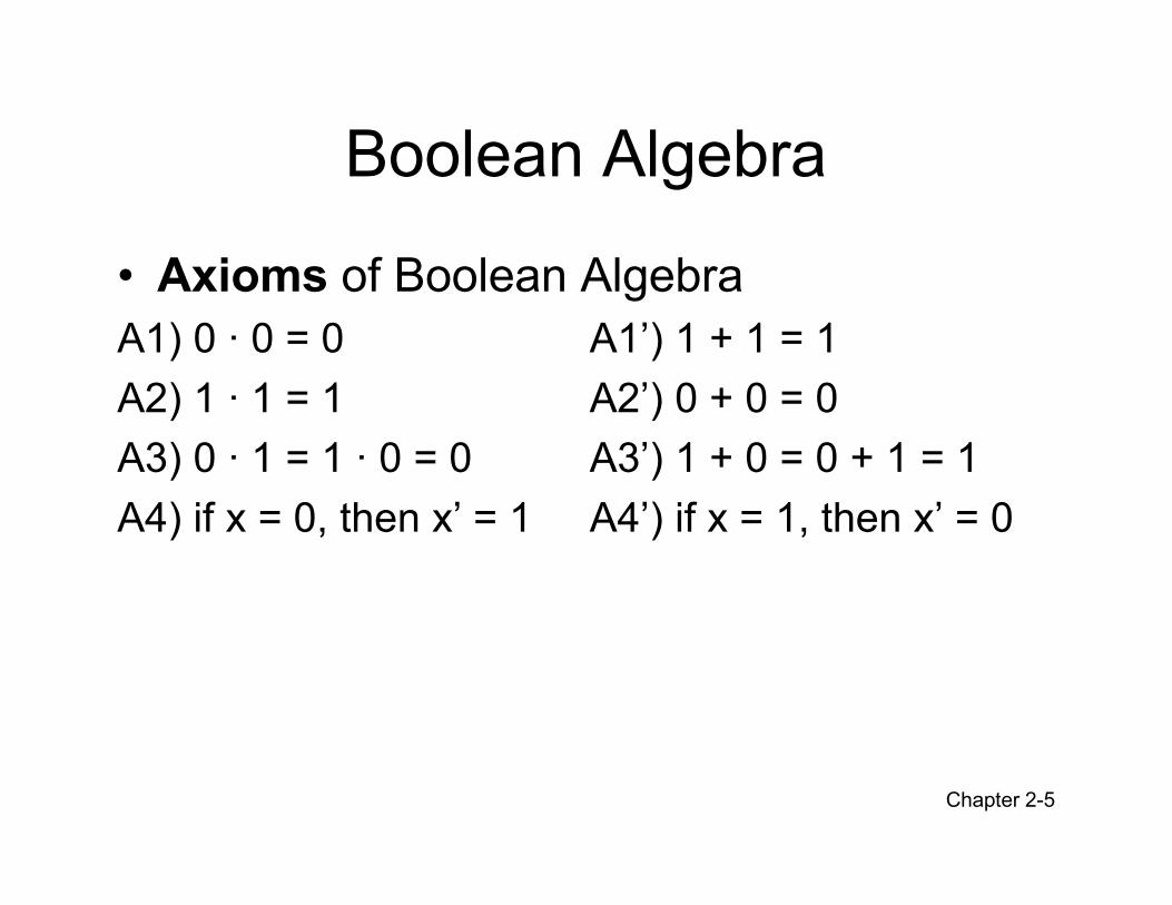
Boolean Algebra
• Axioms of Boolean Algebra
A1) 0 · 0 = 0 A1’) 1 + 1 = 1
A2) 1 · 1 = 1 A2’) 0 + 0 = 0
A3) 0 · 1 = 1 · 0 = 0 A3’) 1 + 0 = 0 + 1 = 1
A4) if x = 0, then x’ = 1 A4’) if x = 1, then x’ = 0
Chapter 2-6
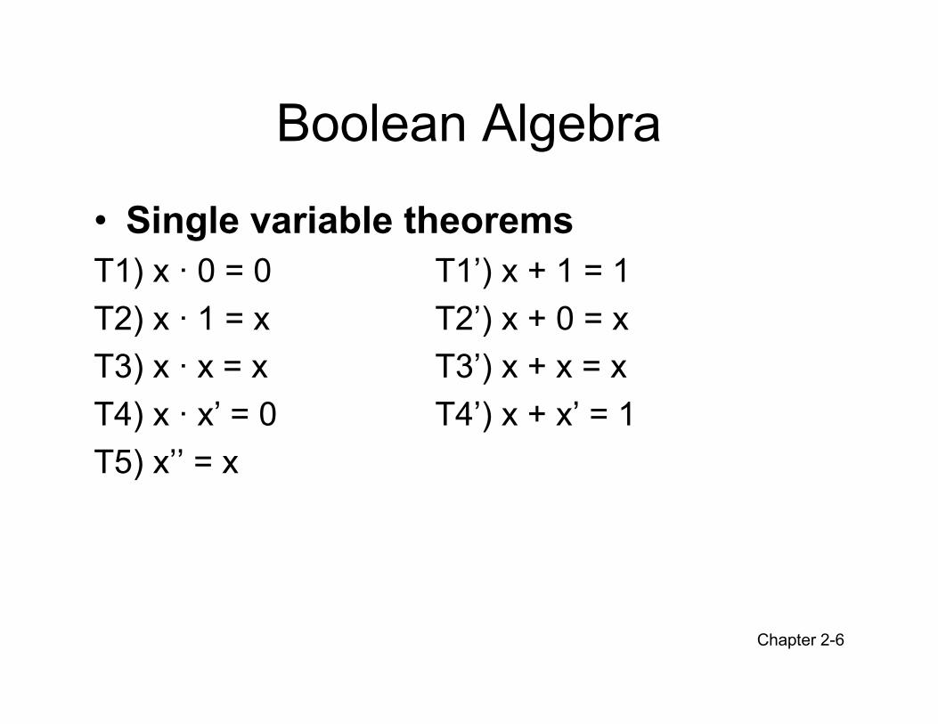
Boolean Algebra
• Single variable theorems
T1) x · 0 = 0 T1’) x + 1 = 1
T2) x · 1 = x T2’) x + 0 = x
T3) x · x = x T3’) x + x = x
T4) x · x’ = 0 T4’) x + x’ = 1
T5) x’’ = x
Chapter 2-7
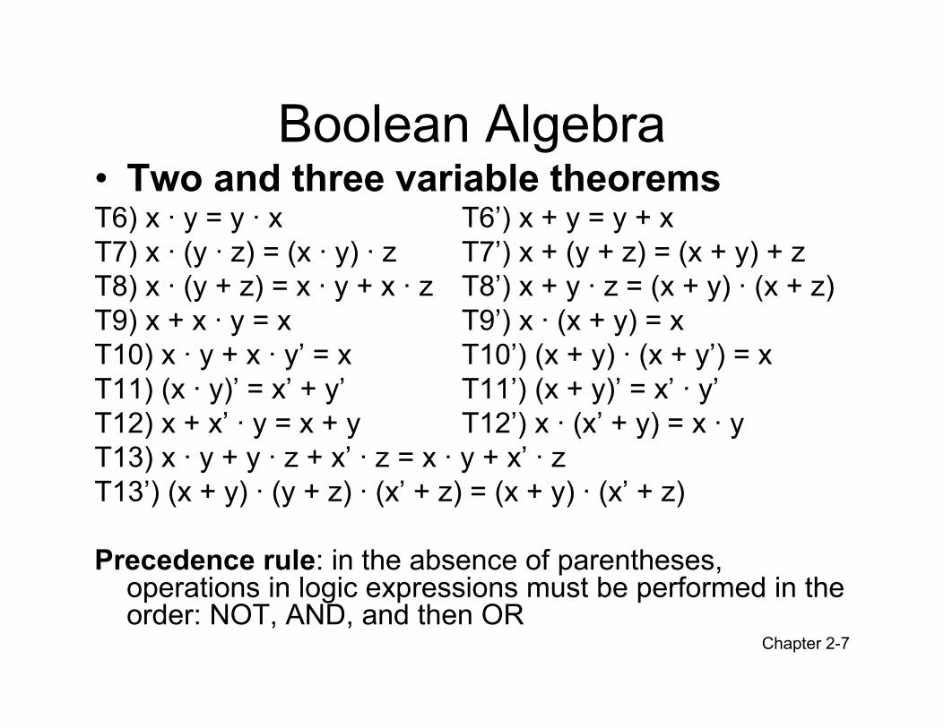
Boolean Algebra• Two and three variable theoremsT6) x · y = y · x T6’) x + y = y + x
T7) x · (y · z) = (x · y) · z T7’) x + (y + z) = (x + y) + z
T8) x · (y + z) = x · y + x · z T8’) x + y · z = (x + y) · (x + z)
T9) x + x · y = x T9’) x · (x + y) = x
T10) x · y + x · y’ = x T10’) (x + y) · (x + y’) = x
T11) (x · y)’ = x’ + y’ T11’) (x + y)’ = x’ · y’
T12) x + x’ · y = x + y T12’) x · (x’ + y) = x · y
T13) x · y + y · z + x’ · z = x · y + x’ · z
T13’) (x + y) · (y + z) · (x’ + z) = (x + y) · (x’ + z)
Precedence rule: in the absence of parentheses, operations in logic expressions must be performed in the order: NOT, AND, and then OR
Chapter 2-8
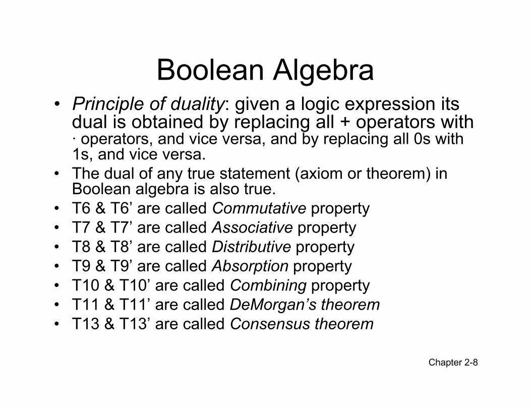
Boolean Algebra• Principle of duality: given a logic expression its dual is obtained by replacing all + operators with · operators, and vice versa, and by replacing all 0s with 1s, and vice versa.
• The dual of any true statement (axiom or theorem) in Boolean algebra is also true.
• T6 & T6’ are called Commutative property
• T7 & T7’ are called Associative property
• T8 & T8’ are called Distributive property
• T9 & T9’ are called Absorption property
• T10 & T10’ are called Combining property
• T11 & T11’ are called DeMorgan’s theorem
• T13 & T13’ are called Consensus theorem
Chapter 2-9
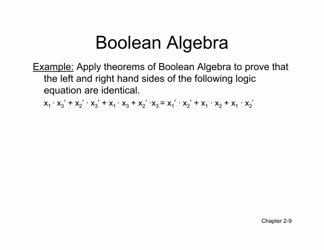
Boolean Algebra
Example: Apply theorems of Boolean Algebra to prove that
the left and right hand sides of the following logic
equation are identical.
x1 · x3’ + x2’ · x3’ + x1 · x3 + x2’ ·x3 = x1’ · x2’ + x1 · x2 + x1 · x2’
Chapter 2-10
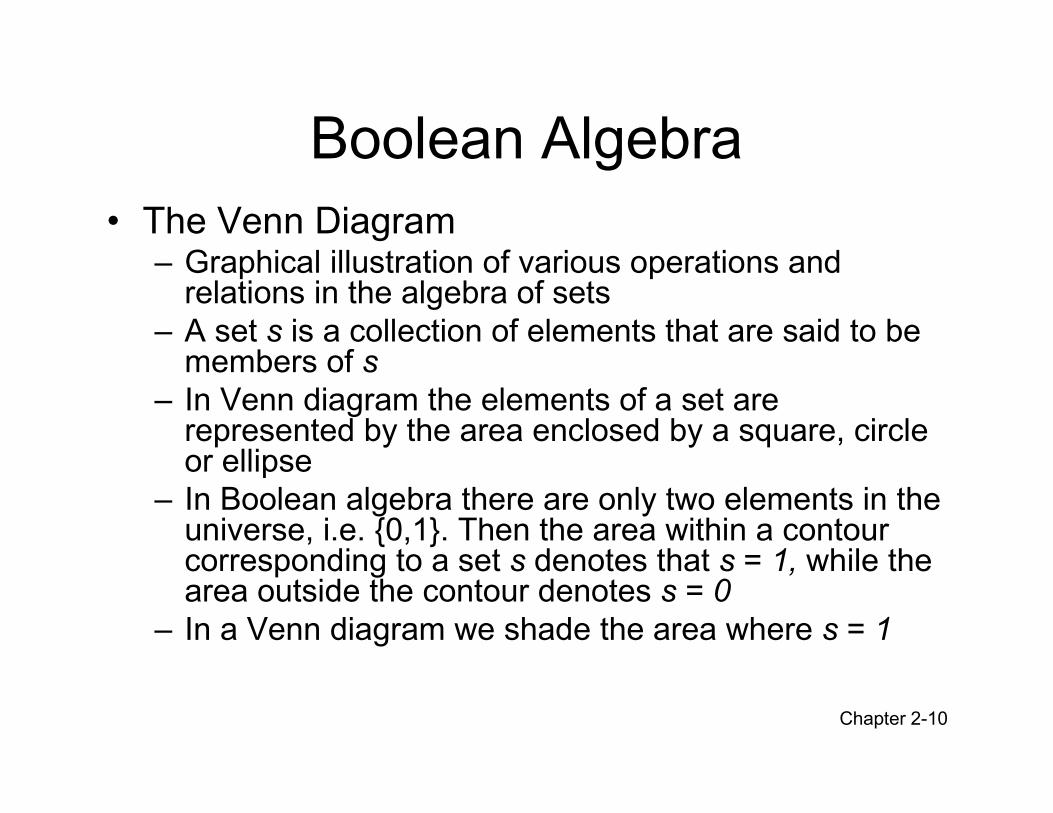
Boolean Algebra
• The Venn Diagram– Graphical illustration of various operations and relations in the algebra of sets
– A set s is a collection of elements that are said to be members of s
– In Venn diagram the elements of a set are represented by the area enclosed by a square, circle or ellipse
– In Boolean algebra there are only two elements in the universe, i.e. {0,1}. Then the area within a contour corresponding to a set s denotes that s = 1, while the area outside the contour denotes s = 0
– In a Venn diagram we shade the area where s = 1
Chapter 2-11
x
Boolean Algebra
x y
z x
x y x y
x x x
(a) Constant 1 (b) Constant 0
(c) Variable x (d)
(e) (f)
(g) (h)
x y ⋅ x y +
x y z + ⋅ x y ⋅
y
x
x y
z
x y
z
x y
z
x y
z
x y
z
x y
z
x x y ⋅
x y ⋅ x + z ⋅ x y z + ( ) ⋅
(a) (d)
(c) (f)
x z ⋅ y z + (b) (e)
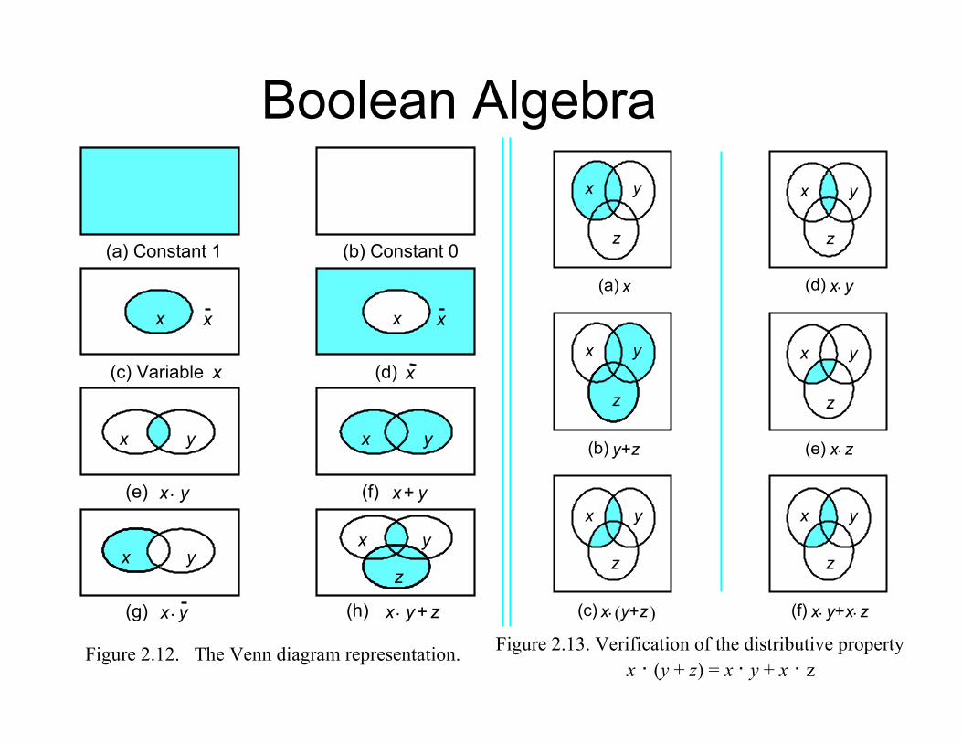
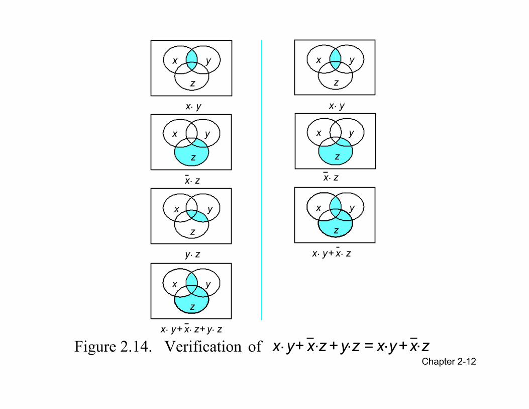
Figure 2.12. The Venn diagram representation.Figure 2.13. Verification of the distributive property
x · (y + z) = x · y + x · z
Chapter 2-12
x y
z
y x
z
x y
z
x y ⋅
y z ⋅
x z ⋅
x y
z
x y ⋅
x y ⋅ x + z y z ⋅ + ⋅
x y
z
x z ⋅
x y ⋅ x + z ⋅
y
z
x
y
z
x
Figure 2.14. Verification of x y · x + z y z = ·+ · x y · x + z·
Chapter 2-13
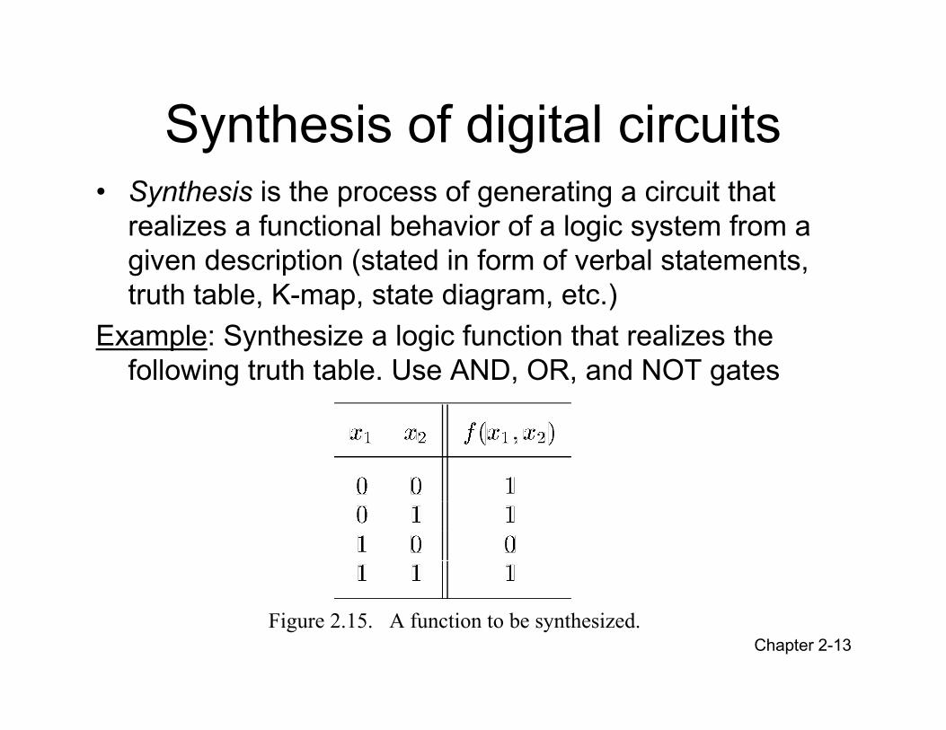
Synthesis of digital circuits• Synthesis is the process of generating a circuit that
realizes a functional behavior of a logic system from a
given description (stated in form of verbal statements,
truth table, K-map, state diagram, etc.)
Example: Synthesize a logic function that realizes the
following truth table. Use AND, OR, and NOT gates
Figure 2.15. A function to be synthesized.
Chapter 2-14
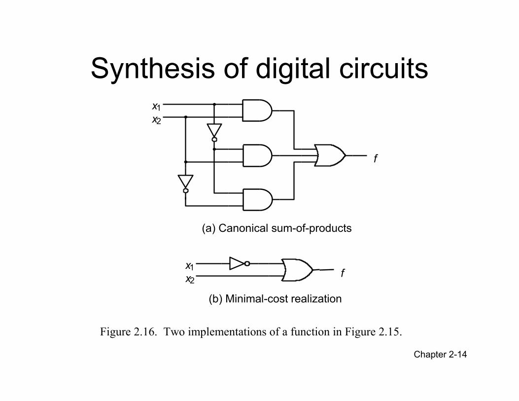
Synthesis of digital circuits
f
(a) Canonical sum-of-products
f
(b) Minimal-cost realization
x 2
x 1
x 1 x 2
Figure 2.16. Two implementations of a function in Figure 2.15.
Chapter 2-15
Synthesis of digital circuitsTerminologies:
• Literal: a variable or the complement of a variable
• Product term: a single literal or logical product (AND) of two or more literals
• n-variable minterm: a product term with n literals. It assumes a value of 1 for exactly one row of a function’s truth table (i.e. input combination)
• Sum-of-products (SOP): logical sum (OR) of product (AND) terms
• Canonical SOP: An SOP where each product term is a minterm.
• Sum term: a single literal or a logical sum of two or more literals.
• n-variable maxterm: a sum term with n literals. It assumes a value of 0 for exactlyone row of a function’s truth table (i.e. input combination)
• Product-of-sums (POS): is logical product of sum terms
• Canonical POS: A POS where each sum term is a maxterm
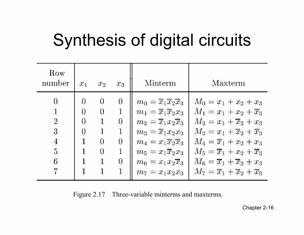
Chapter 2-16
Synthesis of digital circuits
Figure 2.17 Three-variable minterms and maxterms.
Chapter 2-17
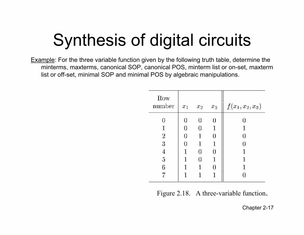
Synthesis of digital circuitsExample: For the three variable function given by the following truth table, determine the
minterms, maxterms, canonical SOP, canonical POS, minterm list or on-set, maxterm
list or off-set, minimal SOP and minimal POS by algebraic manipulations.
Figure 2.18. A three-variable function.
Chapter 2-18
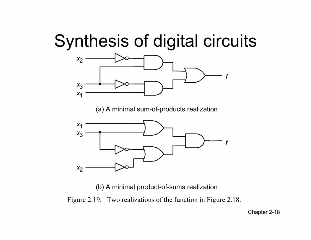
Synthesis of digital circuits
Figure 2.19. Two realizations of the function in Figure 2.18.
f
(a) A minimal sum-of-products realization
f
(b) A minimal product-of-sums realization
x1
x2
x3
x2
x1x3
Chapter 2-19
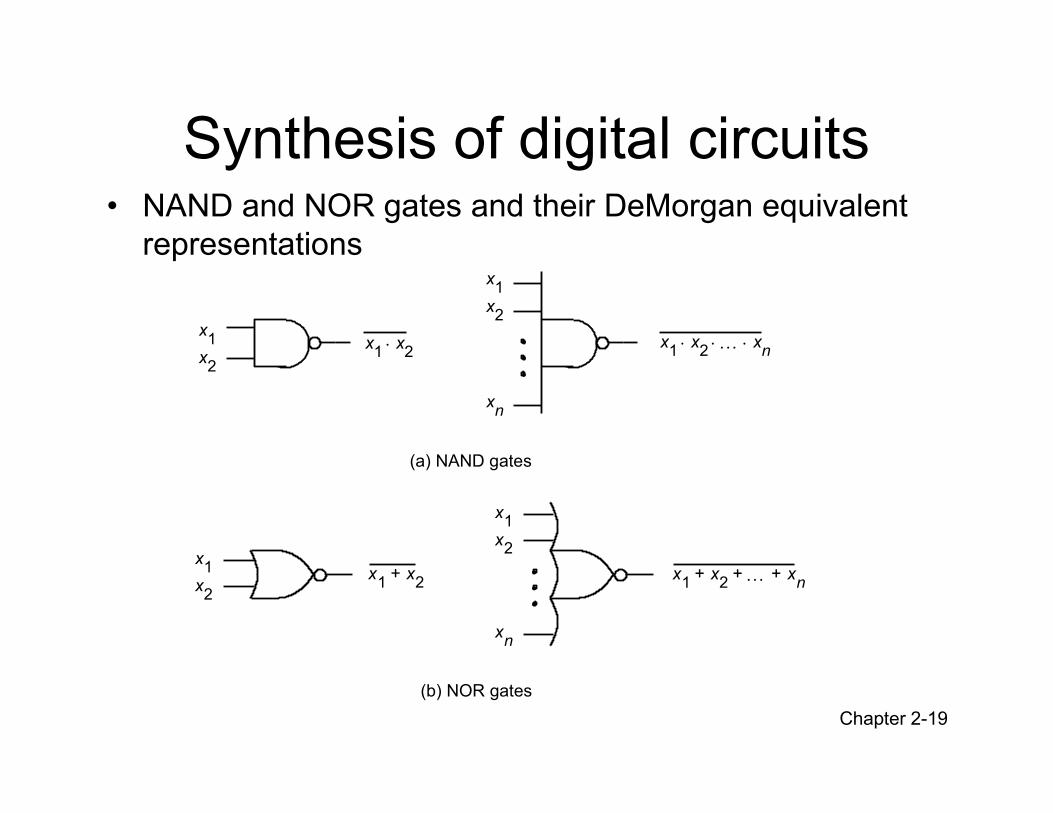
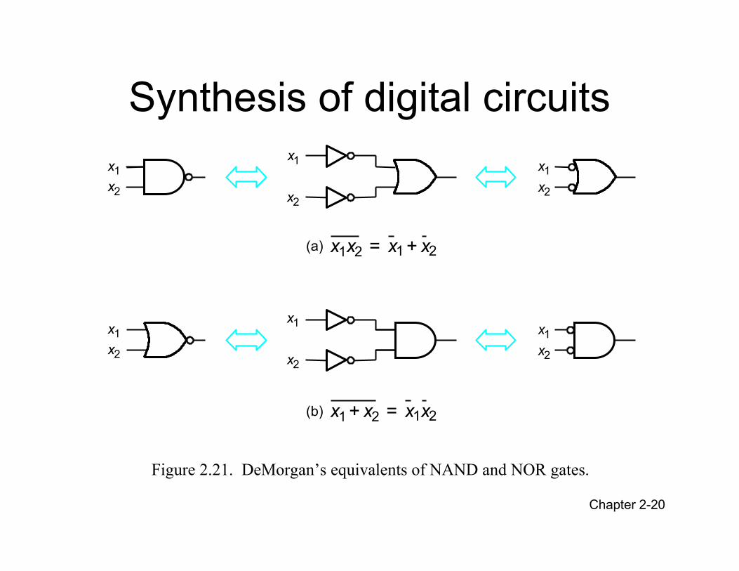
Synthesis of digital circuits• NAND and NOR gates and their DeMorgan equivalent
representationsx 1
x 2
x n
x 1
x 2
x 1
x 2
⋅ x 1
x 2 … x
n ⋅ ⋅ ⋅
(a) NAND gates
x 1
x 2
x n
x 1
x 2 … x
n + + +
x 1
x 2
x 1
x 2
+
(b) NOR gates
Chapter 2-20
Synthesis of digital circuits
x 1
x 2
x 1
x 2
x 1
x 2
x 1
x 2
x 1
x 2
x 1
x 2
x 1 x 2 x 1 x 2 + = (a)
x 1 x 2 + x 1 x 2 = (b)
Figure 2.21. DeMorgan’s equivalents of NAND and NOR gates.
Chapter 2-21
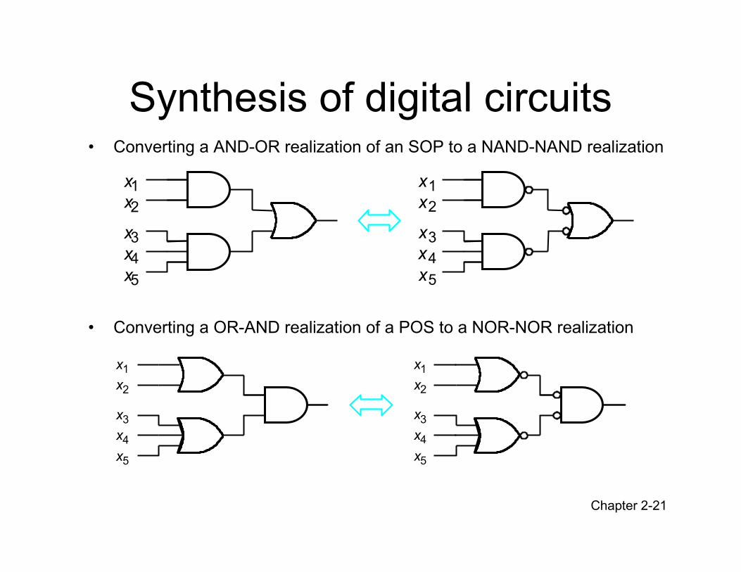
Synthesis of digital circuits• Converting a AND-OR realization of an SOP to a NAND-NAND realization
• Converting a OR-AND realization of a POS to a NOR-NOR realization
x 1 x 2
x 3 x 4 x 5
x 1 x 2
x 3 x 4 x 5
x 1
x 2
x 3
x 4
x 5
x 1
x 2
x 3
x 4
x 5
Chapter 2-22
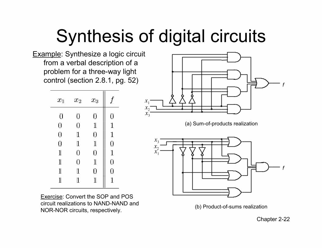
Synthesis of digital circuitsExample: Synthesize a logic circuit
from a verbal description of a
problem for a three-way light
control (section 2.8.1, pg. 52)f
(a) Sum-of-products realization
x1
x3
x2
(b) Product-of-sums realization
f
x3
x1
x2
Exercise: Convert the SOP and POS
circuit realizations to NAND-NAND and
NOR-NOR circuits, respectively.
Chapter 2-23
Introduction to CAD tools• Computer Aided Design (CAD) tools automate the processes of:– Design
– Synthesis
– Optimization
– Simulation:• Functional
• Timing
– Physical implementation
of logic circuits on target devices
• Quartus II from Altera Corporation is such software used in this course.
Chapter 2-24
Introduction to CAD tools• Design entry: description of what the desired circuit is
supposed to do and the formation of its general structure. This step of a design requires design experience & intuition so it is done by a designer.
– Schematic Capture
• graphical entry
– Hardware Description Language (eg. VHDL, Verilog, ABEL)
• Computer program describing how a hardware should behave
• VHDL & Verilog are industry standards and thus portable to different target hardware and CAD tools
• Designer can focus on the functionality of the desired circuit without being overly concerned about the implementation technology
� Both Schematic & HDL design entry methods allow modular and hierarchical designs to manage system complexity
Chapter 2-25
Introduction to CAD tools• Synthesis – process of generating a logic circuit from an
initial specification given in schematic diagram or HDL.
– It involves compiling or translating the design entry (eg. VHDL) into a set of logic expressions that describe the logic functions
– Often the synthesis process is followed by optimization for specified goals: HW cost or time delay
• Functional Simulation – used to verify that the design will function as expected
– Assumes that the logic equations generated during synthesis willbe implemented with perfect gates with no propagation delays
– Test sequences are applied for which the simulator generates outputs
Chapter 2-26
Introduction to CAD tools• Physical Design – the tool determines exactly how to
implement the circuit on a given chip
– Maps a circuit specified in logic expressions into a realizationthat makes use of the resources available on the target chip
– Determines the placement of specific logic elements & their interconnection
• Timing Simulation – a simulation that takes into account the actual delays of signals as they are processed by the logic elements and propagate through the wires
– Helps determine if the generated circuit satisfies the timing requirements of the specification
• Chip Configuration or programming – this step involves the implementation of the circuit on an actual target chip
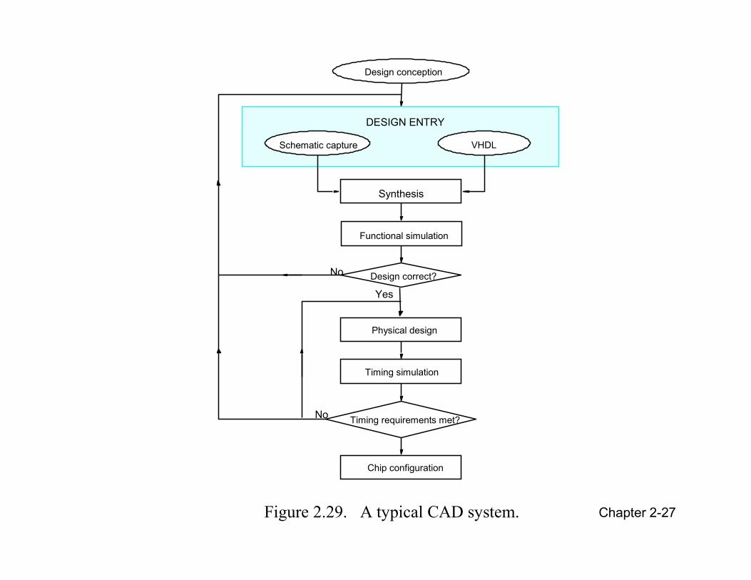
Chapter 2-27Figure 2.29. A typical CAD system.
Design conception
VHDLSchematic capture
DESIGN ENTRY
Design correct?
Functional simulation
No
Yes
No
Synthesis
Physical design
Chip configuration
Timing requirements met?
Timing simulation
Chapter 2-28
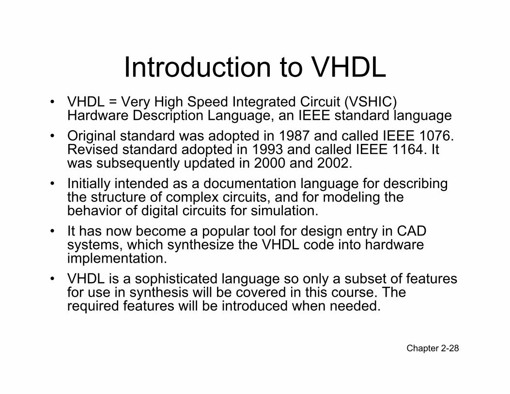
Introduction to VHDL• VHDL = Very High Speed Integrated Circuit (VSHIC)
Hardware Description Language, an IEEE standard language
• Original standard was adopted in 1987 and called IEEE 1076. Revised standard adopted in 1993 and called IEEE 1164. It was subsequently updated in 2000 and 2002.
• Initially intended as a documentation language for describing the structure of complex circuits, and for modeling the behavior of digital circuits for simulation.
• It has now become a popular tool for design entry in CAD systems, which synthesize the VHDL code into hardware implementation.
• VHDL is a sophisticated language so only a subset of features for use in synthesis will be covered in this course. The required features will be introduced when needed.
Chapter 2-29
Introduction to VHDL• Digital signals in VHDL are represented by a data object
of type BIT.
• BIT objects can have only one of two possible values: 0 or 1.
• A VHDL construct called entity is used to declare the input and output interfaces of a circuit or module.
• The entity must be assigned a name.
• The input and output signals for an entity are called its ports, and they are identified by the keyword PORT.
• Each port has an associated mode that specifies whether it is input (IN) to the entity or output (OUT) from the entity.
• Each port is a signal hence has an associated type.
Chapter 2-30
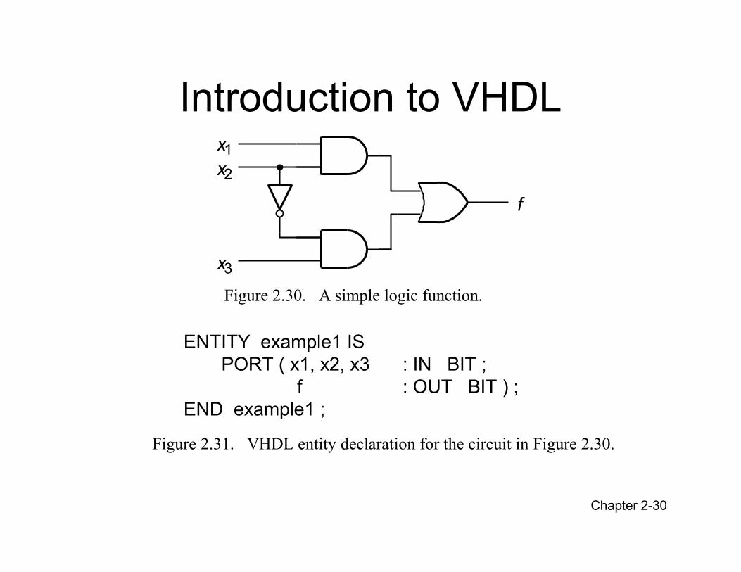
Introduction to VHDL
Figure 2.30. A simple logic function.
f
x3
x1x2
ENTITY example1 IS
PORT ( x1, x2, x3 : IN BIT ;
f : OUT BIT ) ;
END example1 ;
Figure 2.31. VHDL entity declaration for the circuit in Figure 2.30.
Chapter 2-31
Introduction to VHDL
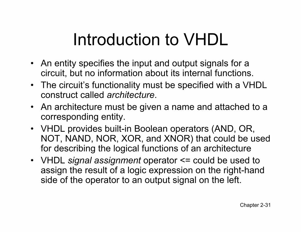
• An entity specifies the input and output signals for a circuit, but no information about its internal functions.
• The circuit’s functionality must be specified with a VHDL construct called architecture.
• An architecture must be given a name and attached to a corresponding entity.
• VHDL provides built-in Boolean operators (AND, OR, NOT, NAND, NOR, XOR, and XNOR) that could be used for describing the logical functions of an architecture
• VHDL signal assignment operator <= could be used to assign the result of a logic expression on the right-hand side of the operator to an output signal on the left.
Chapter 2-32
Introduction to VHDL
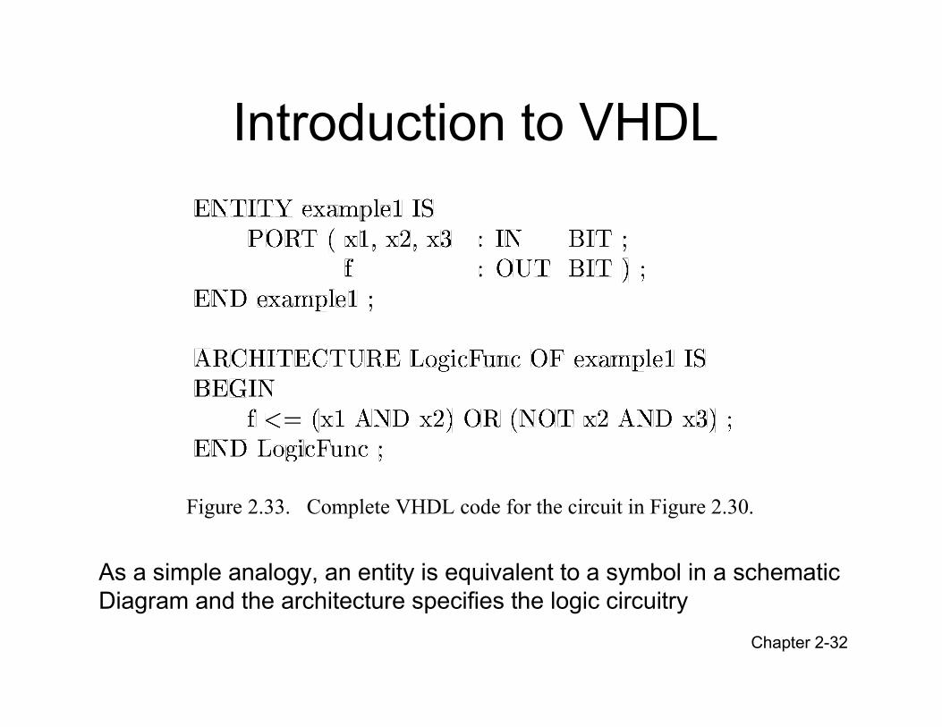
Figure 2.33. Complete VHDL code for the circuit in Figure 2.30.
As a simple analogy, an entity is equivalent to a symbol in a schematic
Diagram and the architecture specifies the logic circuitry
Chapter 2-33
Introduction to VHDL