Embed Size (px)
Citation preview

19
Chapter-2
Fundamental of Partial Discharge &
Measuring Methods
20
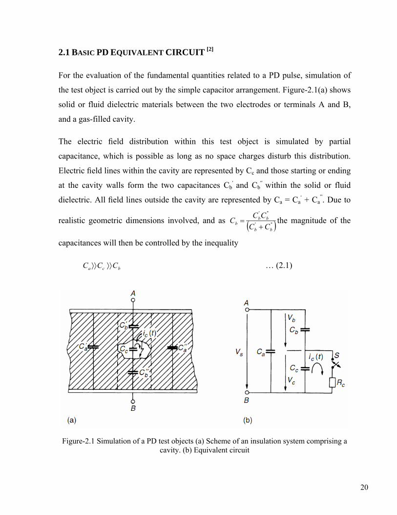
2.1 BASIC PD EQUIVALENT CIRCUIT [2]
For the evaluation of the fundamental quantities related to a PD pulse, simulation of
the test object is carried out by the simple capacitor arrangement. Figure-2.1(a) shows
solid or fluid dielectric materials between the two electrodes or terminals A and B,
and a gas-filled cavity.
The electric field distribution within this test object is simulated by partial
capacitance, which is possible as long as no space charges disturb this distribution.
Electric field lines within the cavity are represented by Cc and those starting or ending
at the cavity walls form the two capacitances Cband Cb ׳
׳׳ within the solid or fluid
dielectric. All field lines outside the cavity are represented by Ca = CaCa + ׳
”. Due to
realistic geometric dimensions involved, and as ( )'''
'''
bb
bbb CC
CCC+
= the magnitude of the
capacitances will then be controlled by the inequality
ca CC ⟩⟩ bC⟩⟩ … (2.1)
Figure-2.1 Simulation of a PD test objects (a) Scheme of an insulation system comprising a cavity. (b) Equivalent circuit
21
This void will become the origin of a PD if the applied voltage is increased and the
field gradients in the void are strongly enhanced by the difference in permittivity as
well as by the shape of the cavity. For an increased value of an A.C. voltage, the
discharge will appear first at the crest or rising part of a half-cycle. This gas discharge
creates electrons as well as negative and positive ions, which are driven to the
surfaces of the void. It forms dipoles or additional polarization of the test object. This
physical effect reduces the voltage across the void significantly. Within the model
these effect causes the cavity capacitance Cc to discharge largely. If the voltage still
increase or decrease by the negative slope of an A.C. voltage, new field lines are built
up and hence the discharge phenomena is repeated during each cycle. If increased
D.C. voltages are applied then one or only a few partial discharges will occur during
the rising part of the voltage. In case of constant voltage, the discharges will stop as
long as the surface charges deposited on the walls of the void do not recombine or
diffuse into the surrounding dielectric.
This phenomenon is simulated by the equivalent circuit that is shown in Figure-2.1(b).
Here, the switch S is controlled by the voltage Vc across the void capacitance Cc, and
S is closed only for a short time, during which the flow of a current ic(t) takes place.
The discharge current ic(t), which cannot be measured, would have a shape as
governed by the gas discharge process and would in general be similar to a Dirac
function, i.e. this discharge current is generally of a very short pulse in the
nanosecond range.
It is assumed that the sample was charged to the voltage Va but the terminals A and B
are no longer connected to a voltage source. If the switch S is closed and Cc becomes
completely discharged then the current ic(t) releases a charge δqc = Cc δVc from Cc, a
charge which is lost in the whole system, assumed for simulation. By comparing the
charges within the system pre and post discharge, it is derived that the voltage drop
across the terminal is
22
( ){ } cbaba VCCCV δδ ×+= / …(2.2)
This voltage drop contains no information about the charge δqc, but it is
proportional to CbδVc, a magnitude related to this charge, where Cb increases with the
geometric dimensions of the cavity.
δVa is clearly a quantity that could be measured. It is a negative voltage step with a
rise time depending upon the duration of ic(t). The magnitude of the voltage step is
quite small and although δVc is in a range of 102 to 103 V; but the ratio Cb/Ca will
always be very small according to Eq.2.1. Thus, a direct detection of this voltage by
the measurement input voltage would be a tedious task. The detection circuits are
based upon another quantity, which can immediately be derived from a nearly
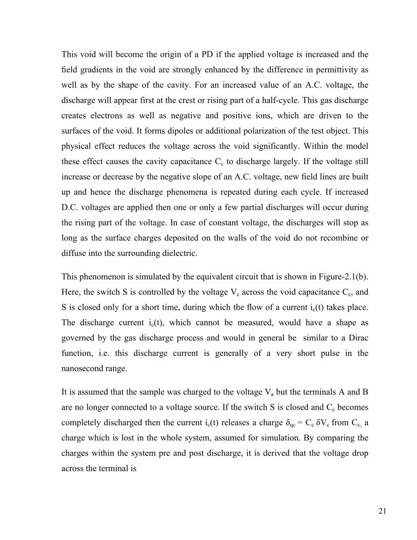
complete circuit shown in Figure-2.2.
The test object (Figure-2.1.a) is now connected to an A.C. voltage source V. An
impedance Z, either comprises only the natural impedance of the lead between
voltage source and the parallel arrangement of Ck and Ct or enlarged by a PD-free
inductance or filter. It may disconnect the ‘coupling capacitor’ Ck and the test
specimen Ct from the voltage source during the short duration PD phenomena and Ck
is a storage capacitor or quite a stable voltage source during the short period of the
partial discharge.
Figure-2.2 The PD test object Ct within a PD test circuit
23
It releases a charging current or the actual ‘PD current pulse’, i(t) between Ck and Ct
and tries to cancel the voltage drop δVa across Ct ≈ (Ca + Cb). If Ck >> Ct, then δVa is
completely compensated and the charge transfer provided by the current pulse i(t) is
given by
( )∫ +== aba VCCtiq δ)( …(2.3)
Therefore,
cb VCq δ= …(2.4)
Hence, it is referred as the apparent charge of a PD pulse, which is the most
fundamental quantity of all PD measurements. The word ‘apparent’ was introduced
because this charge again is not equal to the amount of charge locally involved at the
site of the discharge or cavity Cc. This PD quantity is much more realistic than δVa in
Eq-2.2, as the capacitance Ca of the test object, which is its main part of Ct, has no
influence on it.
In practice, the condition Ck >> Ca (=Ct) is not always applicable. Here, either Ct is
quite large or the loading of an A.C. power supply becomes high and the cost of
building such a large capacitor without PD is not economical. For a finite value of Ck,
the charge q or the current i(t) is reduced, as the voltage across Ck will also drop
during the charge transfer. Designating this voltage drop by δVa*, can be computed by
assuming that the same charge CbδVc has to be transferred in the circuits of Figure-
2.1(b) and figure-2.2 Therefore,
( ) ( )kbabaa CCCVCCV ++=+ *δδ …(2.5)
Using equation (2.2) and (2.4), it is obtained as
24
kba CCCCbV
++=*δ
kba CCCqVc++
=δ …(2.6)
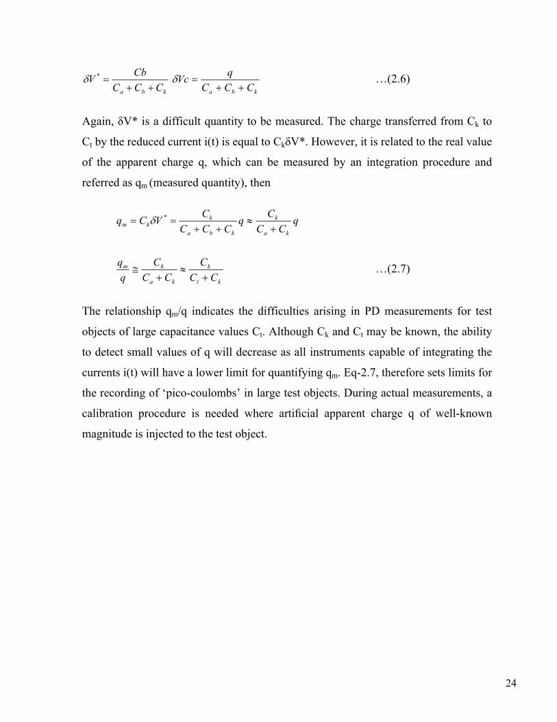
Again, δV* is a difficult quantity to be measured. The charge transferred from Ck to
Ct by the reduced current i(t) is equal to CkδV*. However, it is related to the real value
of the apparent charge q, which can be measured by an integration procedure and
referred as qm (measured quantity), then
qCC
CqCCC
CVCqka
k
kba
kkm +
≈++
== *δ
kt
k
ka
km
CCC
CCC
+≈
+≅ …(2.7)
The relationship qm/q indicates the difficulties arising in PD measurements for test
objects of large capacitance values Ct. Although Ck and Ct may be known, the ability
to detect small values of q will decrease as all instruments capable of integrating the
currents i(t) will have a lower limit for quantifying qm. Eq-2.7, therefore sets limits for
the recording of ‘pico-coulombs’ in large test objects. During actual measurements, a
calibration procedure is needed where artificial apparent charge q of well-known
magnitude is injected to the test object.
25
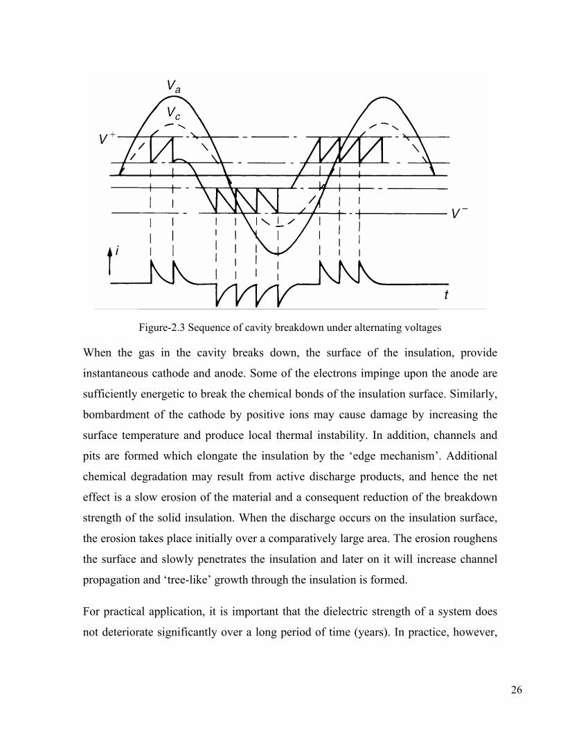
2.2 THE RECURRENCE OF DISCHARGE (DISCHARGE SEQUENCE) [2, 3]
In practice, a cavity in a material is often nearly spherical, and for such cases the
internal field strength is
23
23 EEE
rrc
rc =
+=
εεε …(2.8)
For, εr >> εrc.
Here, E is in the average stress in the dielectric under an applied voltage Va. During
the operation when Vc reaches breakdown value V+ of the gap t then the cavity may
break down. The sequence of breakdown under sinusoidal alternating voltage is
illustrated in Figure-2.3. The dotted curve shows the voltage which would appear
across the cavity if it does not break down. As Vc reaches the value V+, a discharge
takes place, the voltage Vc collapses and the gap extinguishes. The voltage across the
cavity then starts increasing again until it reaches V+ when a new discharge occurs.
Thus, several discharges may take place during the rising part of the applied voltage.
Similarly, on decreasing the applied voltage, the cavity discharges as the voltage
across it reaches V-. In this way, groups of discharges originate from a single cavity
and give rise to positive and negative current pulses on increasing and decreasing of
the voltage respectively.
26
Figure-2.3 Sequence of cavity breakdown under alternating voltages
When the gas in the cavity breaks down, the surface of the insulation, provide
instantaneous cathode and anode. Some of the electrons impinge upon the anode are
sufficiently energetic to break the chemical bonds of the insulation surface. Similarly,
bombardment of the cathode by positive ions may cause damage by increasing the
surface temperature and produce local thermal instability. In addition, channels and
pits are formed which elongate the insulation by the ‘edge mechanism’. Additional
chemical degradation may result from active discharge products, and hence the net
effect is a slow erosion of the material and a consequent reduction of the breakdown
strength of the solid insulation. When the discharge occurs on the insulation surface,
the erosion takes place initially over a comparatively large area. The erosion roughens
the surface and slowly penetrates the insulation and later on it will increase channel
propagation and ‘tree-like’ growth through the insulation is formed.
For practical application, it is important that the dielectric strength of a system does
not deteriorate significantly over a long period of time (years). In practice, however,
27
because of imperfect manufacturing and/or poor design, the dielectric strength
decreases with the time of voltage application (or the life). In many cases, the
decrease in dielectric strength (Eb) with time (t) follows the empirical relationship.
consttE nb = …(2.9)
Where the exponent ‘n’ is derived from the dielectric material, ambient conditions
and the quality of manufacturing.
28
2.3 PD CURRENTS [2]
Before discussing the fundamentals of the measurement of the apparent charge, some
remarks concerning the PD currents i(t) will be helpful, as much of the research work
has been still devoted to these currents, which are difficult to measure with high
accuracy. The difficulties arise for several reasons.
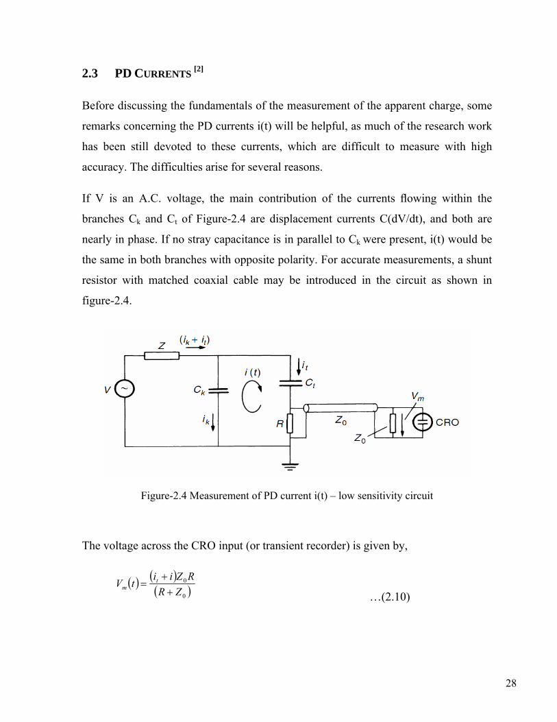
If V is an A.C. voltage, the main contribution of the currents flowing within the
branches Ck and Ct of Figure-2.4 are displacement currents C(dV/dt), and both are
nearly in phase. If no stray capacitance is in parallel to Ck were present, i(t) would be
the same in both branches with opposite polarity. For accurate measurements, a shunt
resistor with matched coaxial cable may be introduced in the circuit as shown in
figure-2.4.
Figure-2.4 Measurement of PD current i(t) – low sensitivity circuit
The voltage across the CRO input (or transient recorder) is given by,
( ) ( )( )0
0
ZRRZiitV t
m ++
= …(2.10)
29
The test object having small capacitance then the voltages referring to the PD currents
i(t) will be clearly distinguished from the displacement currents it(t).
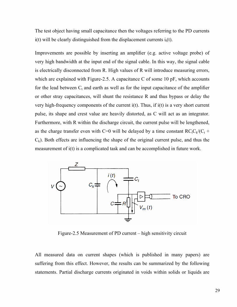
Improvements are possible by inserting an amplifier (e.g. active voltage probe) of
very high bandwidth at the input end of the signal cable. In this way, the signal cable
is electrically disconnected from R. High values of R will introduce measuring errors,
which are explained with Figure-2.5. A capacitance C of some 10 pF, which accounts
for the lead between Ct and earth as well as for the input capacitance of the amplifier
or other stray capacitances, will shunt the resistance R and thus bypass or delay the
very high-frequency components of the current i(t). Thus, if i(t) is a very short current
pulse, its shape and crest value are heavily distorted, as C will act as an integrator.
Furthermore, with R within the discharge circuit, the current pulse will be lengthened,
as the charge transfer even with C=0 will be delayed by a time constant RCtCk/(Ct +
Ck). Both effects are influencing the shape of the original current pulse, and thus the
measurement of i(t) is a complicated task and can be accomplished in future work.
Figure-2.5 Measurement of PD current – high sensitivity circuit
All measured data on current shapes (which is published in many papers) are
suffering from this effect. However, the results can be summarized by the following
statements. Partial discharge currents originated in voids within solids or liquids are
30
very short current pulses of less than a few nanoseconds duration. This can be
understood, as the gas discharge process within a very limited space is developed in a
very short time and is terminated by the limited space for movement of the charge
carriers. Discharges within a homogeneous dielectric material, i.e. a gas, produce PD
currents with a very short rise time (≤5 ns) and a longer tail. Whereas the fast current
rise is produced by the fast avalanche processes, the decay of the current can be
attributed to the drift velocity of attached electrons and positive ions within the
dielectric.
Discharge pulses in atmospheric air provide in general current pulses of less than
about 100 nsec duration. Longer current pulses have only been measured for partial
discharges in fluids or solid materials without pronounced voids, if a number of
consecutive discharges take place within a short time. In most of these cases, the total
duration of i(t) is less than about 1 µsec, with only some exceptions e.g. the usual
bursts of discharges in insulating fluids.
All these statements refer to test circuits with very low inductance and proper
damping effects within the loop Ck − Ct. However, The current i(t) may oscillate and
oscillations are readily excited by the sudden voltage drop across Ct. Test objects with
inherent inductivity or internal resonant circuits, e.g. transformer or reactor/generator
windings, will always cause oscillatory PD current pulses. Such distortions of the PD
currents, however, do not change the transferred charge magnitudes, as no discharge
resistor is in parallel to Ck or Ct. If the displacement currents it(t) or ik(t) are
suppressed, the distorted PD currents can also be filtered, integrated and displayed.
31
2.4 VARIOUS PD QUANTITIES [2, 3]
Partial discharge in any test object under given condition may be characterized
by different measurable quantities like charge, repetition rate or integrated quantities
etc.
Apparent Charge (q):
The apparent charge q of a partial discharge is that charge which if injected
instantaneously between the terminals of the test object, would momentarily change
the voltage between its terminals by the same amount as the partial discharge itself
and is expresses in pico coulombs. Final note is made with reference to the definition
of the apparent charge q (as given in the new IEC Standard 60270) is not equal to the
amount of charge locally involved at the site of the discharge and which cannot be
measured directly.
Repetition Rate (n):
It is the average number of partial discharge pulses per second measured over a
selected time. In practice, only pulses above a specified magnitude or within a
specified range of magnitudes may be considered.
Specified PD Magnitude:
It is the value the PD quantity stated in standards for the given test object at a
specified voltage.
Partial Discharge Inception Voltage (Vi):
It is the lowest voltage at which PDs are observed in test arrangement,(in
practice, lowest value at which PD' magnitude becomes equal to or exceeds a
specified low value) when the voltage applied, to the object is gradually increased
from a lower value at which no such discharges are observed,'
32
Partial Discharge Extinction Voltage (Ve):
It is the lowest voltage at which no PDs are observed in the test arrangement,
(in practice, reduced below a specified value) when the voltage applied to the object is
gradually decreased from a higher value at which such discharges are observed.
Partial Discharge Test Voltage:
PD test voltage is a specified voltage, applied in a specified test procedure,
during which the test object should not exhibit partial discharges exceeding a
specified magnitude.
The Average Discharge Current (I):
It is the sum of the absolute values of the apparent charges during a certain
time interval divided by this time interval.
( )iref
qqqT
I +++= .........121 …(2.12)
The Quadratic Rate D:
It is the sum of the squares of the apparent charges during a certain time
interval divided by this time interval.
D=l/Tref ( q12+q2
2+ … + qi2) …(2.13)
The Discharge Power p:
It is the average power fed into the terminals of the test object due to partial
discharges.
D=l/Tref ( q1 u1 +q2 u2 + … + qi ui) …(2.14)
33
Where u1, u2, … , un are instantaneous values of the test voltage at the instants
of occurrence ti of the individual apparent charge magnitudes qi.
Additional quantities related to PD pulses, although already mentioned in earlier
standards, will be used extensively in the future and thus their definitions are given
below with brief comments only:
(a) The phase angle Φi and time ti is the occurrence of a PD pulse is
⎟⎠⎞
⎜⎝⎛=
Tti
i 360φ …(2.15)
Where ti is the time measured between the preceding positive going transition of the
test voltage through zero and the PD pulse. Here T is the period of the test voltage.

34
2.5 VARIOUS PD MEASUREMENT METHODS [2, 3]
The detection and measurement of discharges is based on the exchange of energy
transform during the discharge. These exchanges include:
− Electrical pulse currents (with some exceptions, i.e. some types of glow
discharges)
− Dielectric losses
− Electromagnetic radiation (light)
− Sound (noise)
− Increased gas pressure
− Chemical reactions
Therefore, discharge detection and measuring techniques may be based on the
observation of any of the above phenomena.
Non-electrical methods of partial discharge detection include acoustical,
optical and chemical methods and also the subsequent observation of the effects of
any discharges on the test object. In general, these methods are not suitable for
quantitative measurement of partial discharge quantities as defined in the standard by
electrical measurement methods, but they are essentially used to detect and/or to
locate the discharges.
Acoustic Detection:
Aural observations made in a room with low noise level may be used as a
means of detecting partial discharges.
35
Visual or Optical Detection:
Visual observations can be carried out in a darkened room, after the eyes have
become adapted to the dark and, if necessary, with the aid of binoculars of large
aperture.
Chemical Detection:
The presence of partial discharges in oil or gas insulated apparatus may be
detected in some cases by the analysis of the decomposition products dissolved in the
oil or in the gas. These products accumulate during prolonged operation, so chemical
analysis may be applicable to estimate the degradation, which has been caused by
partial discharges.
The oldest and simplest method relies on listening to the acoustic noise from the
discharge, the ‘hissing test’. This scheme has lower sensitivity and difficulties arise in
distinguishing between discharges and extraneous noise sources, particularly when
tests are carried out on factory premises. The use of optical techniques is limited to
discharges within transparent media and thus not applicable in most of the cases.
Latest acoustical detection methods utilize ultrasonic transducers, which can be used
to localize the discharges.
The most frequently used and successful detection methods are the electrical
ones where new IEC Standard is also related. These methods are aimed to separate the
impulse currents linked with partial discharges from any other phenomena. The
adequate applications of PD detectors are well defined and presume a fundamental
knowledge of the electrical phenomena within the test samples and the test circuits.
Electrical PD detection methods are based on the appearance of a ‘PD pulse’ at the
terminals of a test object, which may be either a simple dielectric test specimen for
fundamental investigations or even a large HV apparatus which has to undergo a PD
test.
36
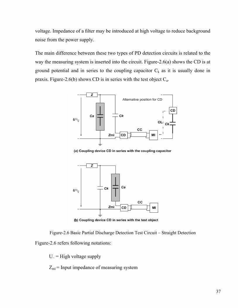
2.6 PD MEASURING SYSTEM WITHIN THE PD TEST CIRCUIT [2]
In above sections the evolution of the PD current pulses and measurement procedures
of these pulses have been broadly discussed. To quantify the individual apparent
charge magnitudes qi for the repeatedly occurring PD pulses; (which may have quite
specific statistical distributions) a measuring system must be integrated into the test
circuit. Already at this point, it shall be mentioned that under practical environment
conditions, quite different kinds of disturbances (background noise) are present,
which will be summarized in later section.
Most PD measuring systems applied are integrated into the test circuit in accordance
with schemes shown in Figure-2.6(a) and Figure-2.6(b), which are taken from the new
IEC Standard. Within these ‘straight detection circuits’, the coupling device ‘CD’
with its input impedance ‘Zmi’ forms the input end of the measuring system.
As indicated in Figure-2.6(a), this device may also be placed at the high-voltage
terminal side, provided if the test object has one terminal earthed. Optical links are
then used to connect the CD with an instrument instead of a connecting cable ‘CC’.
Some essential requirements and explanations with reference to these figures as
indicated by the standard are cited here:
The coupling capacitor Ck shall be of low inductance design and should exhibit a
sufficiently low level of partial discharges at the specified test voltage to allow the
measurement of the specified partial discharge magnitude. A higher level of partial
discharges can be tolerated if the measuring system is capable of separating the
discharges from the test object and the coupling capacitor and measuring them
separately.
The high voltage supply shall have sufficiently low level of background noise to
allow the specified partial discharge magnitude to be measured at the specified test
37
voltage. Impedance of a filter may be introduced at high voltage to reduce background
noise from the power supply.
The main difference between these two types of PD detection circuits is related to the
way the measuring system is inserted into the circuit. Figure-2.6(a) shows the CD is at
ground potential and in series to the coupling capacitor Ck as it is usually done in
praxis. Figure-2.6(b) shows CD is in series with the test object Ca.
Figure-2.6 Basic Partial Discharge Detection Test Circuit – Straight Detection
Figure-2.6 refers following notations:
U~ = High voltage supply
Zmi = Input impedance of measuring system
38
CC = connecting cable
OL = optical link
Ca = test object
Ck = coupling capacitor
CD = coupling device
MI = measuring instrument
Here, the stray capacitances of all elements of the high-voltage side to ground
potential will increase the value of Ck providing a somewhat higher sensitivity for this
circuit according to equation-2.7.The disadvantage is the possibility of damage to the
PD measuring system, if the test object fails. The transfer impedance Z(f) is the ratio
of the output voltage amplitude to a constant input current amplitude, as a function of
frequency f, when the input is sinusoidal. This definition is due to the fact that any
kind of output signal of a measuring instrument (MI) as used for monitoring PD
signals is controlled by a voltage, whereas the input at the CD is a current.
The lower and upper limit frequencies f1 and f2 are the frequencies at which the
transfer impedance Z(f) has fallen by 6 dB from the peak pass band value. Mid-band
frequency fm and bandwidth Δf for all kinds of measuring systems, the mid-band
frequency is defined by,
( )2
21 fffm+
= …(2.16)
and the bandwidth by,
12 fff −=Δ …(2.17)
The superposition error is caused by the overlapping of transient output pulse
responses when the time interval between input current pulses is less than the duration
39
of a single output response pulse. Superposition errors may be additive or subtractive
depending on the pulse repetition rate ‘n’ of the input pulses. In practical circuits, both
types will occur due to the random nature of the pulse repetition rate. This rate ‘n’ is
defined as the ratio of total number of PD pulses recorded in a selected time interval
to the duration of the time interval.
The pulse resolution time Tr is the shortest time interval between two consecutive
input pulses of very short duration, of same shape, polarity and charge magnitude for
which the peak value of the resulting response will change by not more than 10 per
cent of that for a single pulse. The pulse resolution time is in general inversely
proportional to the bandwidth Δf of the measuring system. It is an indication of the
measuring system’s ability to resolve successive PD events.
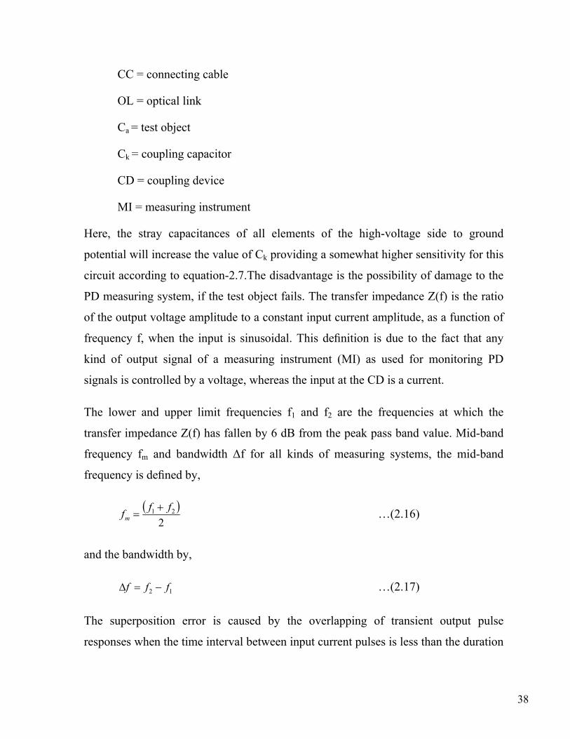
Figure-2.7 shows correct relationship between amplitude and frequency to minimize
integration errors for a wide-band system. The integration error is the error in
apparent charge measurement, which occurs when the upper frequency limit of the
PD current pulse amplitude spectrum is lower than (i) the upper cut-off frequency of a
wideband measuring system or (ii) the mid-band frequency of a narrow-band
measuring system.
Figure-2.7 Correct Relationship Between Amplitude and Frequency to Minimize Integration Errors for a Wide-band System
40
As shown in figure-2.7,
A is a band-pass of the measuring system
B is an amplitude frequency spectrum of the PD pulse
C is an amplitude frequency spectrum of calibration pulse
f1 is lower limit frequency
f2 is upper limit frequency
PD measuring systems quantifying apparent charge magnitudes are band-pass
systems, which predominantly are able to suppress the high power frequency
displacement currents including higher harmonics.
The lower frequency limit of the band-pass f1 and the kind of ‘roll-off’ of the
bandpass control this ability. Adequate integration can thus only be made if the ‘pass-
band’ of the filter is still within the constant part of the amplitude frequency spectrum
of the PD pulse to be measured. Next topic discusses basic types of PD instruments to
measure PD.
MEASURING SYSTEM FOR APPARENT CHARGE
The following type of measuring system comprises subsystems like, coupling device
(CD), transmission system or connecting cable (CC), and a measuring instrument
(MI) as seen in figure-2.6. In general the transmission system, necessary to transmit
the output signal of the CD to the input of the MI, does not contribute to the
measuring system characteristics as both ends are matched to the characteristics of
both elements. The CC will thus not be considered further.
41
The input impedance Zmi of the CD or measuring system respectively will have some
influence on the waveshape of the PD current pulse i(t), which is already mentioned
in the figure-2.5 description. The high input impedance will delay the charge transfer
between Ca and Ck to such an extent that the upper limit frequency of the amplitude
frequency spectrum would drop to unacceptable low values. Often, values of Zmi are
in the range of 100 Ω. In common with the first two measuring systems for apparent
charge is a newly defined ‘pulse train response’ of the instruments to quantify the
‘largest repeatedly occurring PD magnitude’, which is taken as a measure of the
‘specified partial discharge magnitude’ , permitted in test objects during acceptance
tests under specified test conditions.
Sequences of partial discharges follow in general unknown statistical distributions and
it would be useless to quantify only one or very few discharges of large magnitude
within a large array of much smaller events as a specified PD magnitude. For further
information on quantitative requirements about this pulse train response, which was
not specified up to now and thus may not be found within in earlier instruments.
WIDE BAND PD INSTRUMENTS
Up to 1999, no specifications or recommendations concerning to permitted response
parameters have been available. Now, the following parameters are recommended. In
combination with the CD, wide-band PD measuring systems, which are characterized
by a transfer impedance Z(f) having fixed values of the lower and upper limit
frequencies f1 and f2, and adequate attenuation below f1 and above f2, shall be
designed to have the following values for f1, f2 and Δf:
30 kHz ≤ f1 ≤ 100 kHz;
f2 ≤ 500 kHz;
100 kHz ≤ Δf ≤ 400 kHz;
42
The response of these instruments to a (non-oscillating) PD current pulse is in general
a well-damped oscillation as shown below. Both the apparent charge q and with some
reservation the polarity of the PD current pulse can be determined from this response.
The pulse resolution time Tr is small and is typically 5−20 µs.
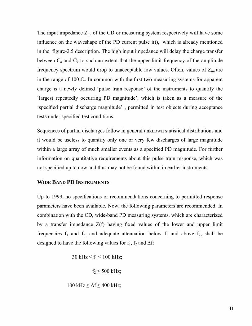
Figure-2.8 shows the typical principle of such a system and Figure-2.8(a) shows
simplified equivalent circuit for the CD and amplifier whereas Figure-2.8(b) shows
typical time-dependent quantities within (a) (T = period of power frequency; τ = pulse
resolution time Tr )
Figure-2.8 Principle of ‘Wide-band’ PD Measuring System
43
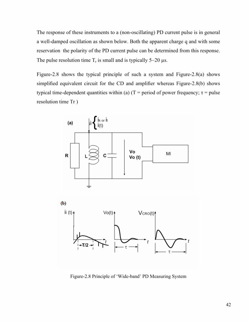
The coupling devices CD (Figure-2.6) are passive high-pass systems but behave more
often as a parallel R-L-C resonance circuit (Figure-2.8(a)) whose quality factor is
relatively low. Such coupling impedance provides two important qualities.
At first, a simple calculation, which is the ratio of output voltage V0 to input current Ii
in dependency of frequency (= transfer impedance Z(f)) would readily demonstrate an
adequate suppression of low and high frequency currents in the neighborhood of its
resonance frequency. For a quality factor of Q = 1, this attenuation is already
−20dB/decade and could be greatly increased close to resonance frequency by
increasing the values of Q. Secondly, this parallel circuit also performs an integration
of the PD currents i(t), as this circuit is already a simple band-pass filter and can be
used as an integrating device.
Let us assume that the PD current pulse i(t) will not be influenced by the test circuit
and would be of an extremely short duration pulse ,simulated by a Dirac function
comprising the apparent charge q. Then the calculation of the output voltage V0(t)
according to Figure-2.8(a) results in:
⎥⎦
⎤⎢⎣
⎡−= − tte
CqtV t β
βαβα sincos)(0 …(2.18)
Where,
RC21
=α ; LCLC
20
2 11 αωαβ −=−= …(2.19)
This equation displays a damped oscillatory output voltage, whose amplitudes are
proportional to q. The integration of i(t) is thus performed instantaneously( t=0) by the
capacitance C, but the oscillations, if not damped, would heavily increase the ‘pulse
resolution time Tr ’ of the measuring circuit and cause ‘superposition errors’ for too
short time intervals between consecutive PD events.
44
With a quality factor of Q = 1, i.e. R = √(L/C), a very efficient damping can be
achieved, since α = ω0/2 = πf0 for a resonance frequency f0 of typically 100 kHz, and
an approximate resolution time of Tr ≅ t = 3/ α, this time becomes about 10 µsec.
For higher Q values, Tr will be longer, but also the filter efficiency will increase and
therefore a compromise is necessary. The resonance frequency f0 is also influenced by
the main test circuit elements Ck and Ca, as their series connection contributes to C.
Therefore the ‘RLC input units’ must be changed according to specimen capacitance
to achieve a bandwidth or resonance frequency f0 within certain limits. These limits
are postulated by the bandwidth Δf of the additional band-pass amplifier connected to
this resonant circuit to increase the sensitivity and thus to provide again an
integration.
These amplifiers are typically designed for lower and upper limit frequencies of some
10 kHz and some 100 kHz respectively, and sometimes the lower limit frequency
range may also be switched from some 10 kHz up to about 150 kHz to further
suppress power frequencies. In general the fixed limit frequencies are thus within a
frequency band and are not used by radio stations and higher than the harmonics of
the power supply voltages.
The band-pass amplifier has in general variable amplification to feed the ‘CRO’
(reading device) following the amplifier with adequate magnitudes during calibration
and measurement. Figure-2.8(b) shows the time-dependent quantities (input a.c.
current with superimposed PD signals, voltages before and after amplification).
Figure-2.9 shows the amplified discharge pulses are in general displayed by an
(analogue or digital) oscilloscope superimposed on a power frequency elliptic time
base. The magnitude of the individual PD pulses is then quantified by comparing the
pulse crest values with those produced during a calibration procedure. With this type
of reading by individual persons it is not possible to quantify the standardized ‘pulse
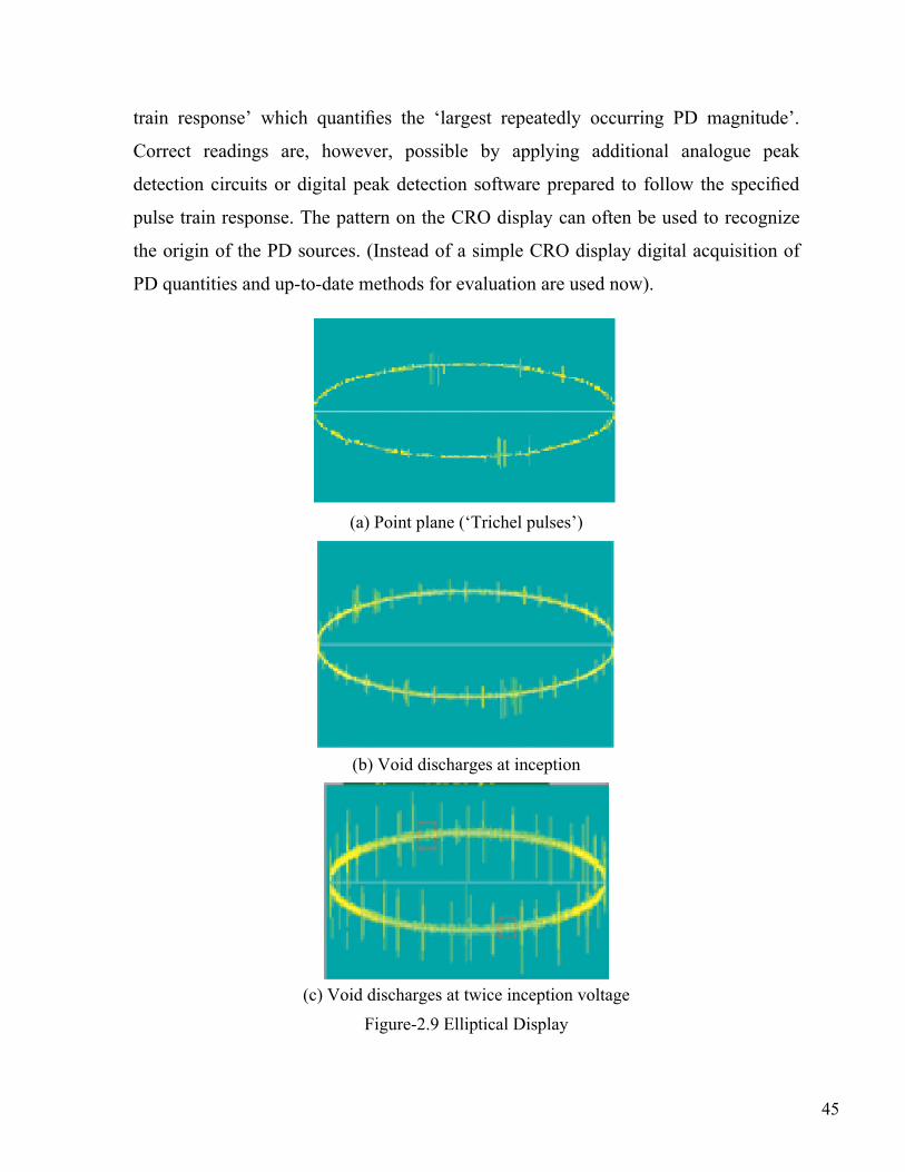
45
train response’ which quantifies the ‘largest repeatedly occurring PD magnitude’.
Correct readings are, however, possible by applying additional analogue peak
detection circuits or digital peak detection software prepared to follow the specified
pulse train response. The pattern on the CRO display can often be used to recognize
the origin of the PD sources. (Instead of a simple CRO display digital acquisition of
PD quantities and up-to-date methods for evaluation are used now).
(a) Point plane (‘Trichel pulses’)
(b) Void discharges at inception
(c) Void discharges at twice inception voltage
Figure-2.9 Elliptical Display
46
A typical pattern of Trichel pulses can be seen in figure-2.9(a). Figure-2.9(b), is
typical for the case for which the pulse resolution time of the measuring system
including the test circuit, which is too large to distinguish between individual PD
pulses.
It was clearly shown that even the response of such ‘wide-band PD instruments’
provide no more information about the original shape of the input PD current pulse as
indicated in figure-2.8(b) and confirmed by the pattern of the Trichel pulses in figure-
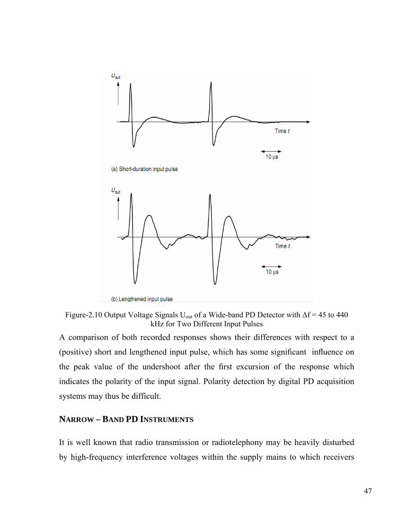
2.9(a). Figure-2.10 further confirms this statement. Figure-2.10 shows two recorded
responses for two consecutive calibration pulses (‘double pulse’) are shown within a
time scale of microseconds.
47
Figure-2.10 Output Voltage Signals Uout of a Wide-band PD Detector with Δf = 45 to 440 kHz for Two Different Input Pulses
A comparison of both recorded responses shows their differences with respect to a
(positive) short and lengthened input pulse, which has some significant influence on
the peak value of the undershoot after the first excursion of the response which
indicates the polarity of the input signal. Polarity detection by digital PD acquisition
systems may thus be difficult.
NARROW – BAND PD INSTRUMENTS
It is well known that radio transmission or radiotelephony may be heavily disturbed
by high-frequency interference voltages within the supply mains to which receivers
48
are connected or by disturbing electromagnetic fields picked up by the aerials. It was
also early recognized that corona discharges at HV transmission lines are the source
of such disturbances. The measurement of ‘radio noise’ in the vicinity of such
transmission lines is thus an old and well-known technique which several decades ago
triggered the application of this measurement technique to detect insulation failures,
i.e. partial discharges, within HV apparatus of any kind.
The methods for the measurement of radio noise or radio disturbance have been
subjected to many modifications during the past decades. Apart from many older
national or international recommendations, the latest ‘specifications for radio
disturbance and immunity measuring apparatus and methods’ within a frequency
range of 10 kHz to 1000 MHz are now described in the CISPR Publication. As
defined in this specification, the expression ‘radio disturbance voltage (RDV)’, earlier
termed as ‘radio noise’, ‘radio influence’ or ‘radio interference’ voltages, is now used
to characterize the measured disturbance quantity.
Narrow-band PD instruments, which are now also specified within the new IEC
Standard for the measurement of the apparent charge, are very similar to those RDV
meters, which are applied for RDV measurements in the frequency range 100 kHz to
30MHz.
The PD instruments are characterized by a small bandwidth Δf and a mid-band
frequency fm, which can be varied over a wider frequency range, where the amplitude
frequency spectrum of the PD current pulses is in general approximately constant.
The recommended values for Δf and fm for PD instruments are
9 kHz ≤ Δf ≤ 30 kHz
50 kHz ≤ fm ≤ 1 MHz
49
It is further recommended that the transfer impedance Z(f) at frequencies of fm ± Δf
should already be 20 dB below the peak pass-band value. Commercial instruments of
this type may be designed for a larger range of mid-band frequencies; therefore, the
standard provides the following note for the user. ‘During actual apparent charge
measurements, mid-band frequencies fm > 1MHz should only be applied if the
readings for such higher values do not differ from those as monitored for the
recommended values of fm’.
This statement denotes that only the constant part of the PD current amplitude\
frequency spectrum is an image of the apparent charge. As shown below in more
detail, the response of these instruments to a PD current pulse is a transient oscillation
with the positive and negative peak values of its envelope proportional to the apparent
charge, independent of the polarity of this charge.
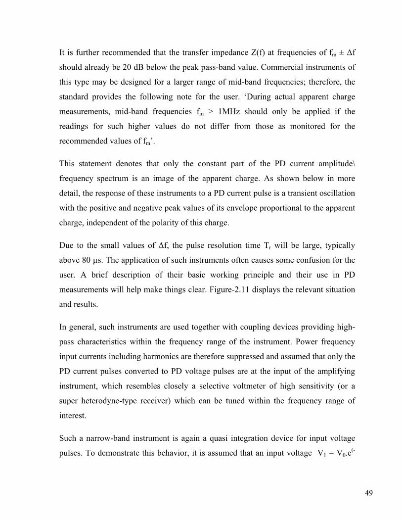
Due to the small values of Δf, the pulse resolution time Tr will be large, typically
above 80 µs. The application of such instruments often causes some confusion for the
user. A brief description of their basic working principle and their use in PD
measurements will help make things clear. Figure-2.11 displays the relevant situation
and results.
In general, such instruments are used together with coupling devices providing high-
pass characteristics within the frequency range of the instrument. Power frequency
input currents including harmonics are therefore suppressed and assumed that only the
PD current pulses converted to PD voltage pulses are at the input of the amplifying
instrument, which resembles closely a selective voltmeter of high sensitivity (or a
super heterodyne-type receiver) which can be tuned within the frequency range of
interest.
Such a narrow-band instrument is again a quasi integration device for input voltage
pulses. To demonstrate this behavior, it is assumed that an input voltage V1 = V0.e(-
50
t/T), i. e. an exponentially decaying input pulse which starts suddenly with amplitude
V0 (see Figure-2.11(b)). The integral of this pulse, ∫∞
0
v1(t) dt, is V0T and is thus a
quantity proportional to the apparent charge q of a PD current pulse. The complex
frequency spectrum of this impulse is then given by applying the Fourier integral
( ) ( ) ( )Tj
TSTj
TVdttjtvjV
ωωωω
+=
+=−= ∫
∞
11exp 00
011 …(2.20)
and the amplitude frequency spectrum | V1 (iω) | by
( )( ) ( )2
02
01
11 T
S
T
TVjVωω
ω+
=+
= …(2.21)
where S0 is proportional to q. From the amplitude frequency spectrum, sketched in
Figure-2.11(c), it is obvious that the amplitudes decay already to -3 dB or more than
about 30 per cent for the angular frequency of ωc > (1/T). This critical frequency fc is
for T = 0.1 µsec only 1.6 MHz, a value which can be assumed for many PD impulses.
51
Figure-2.11 Narrow-band Amplifiers Responses (Part-1)
52
Figure 2.11 Narrow-band Amplifiers Responses (Part-2)
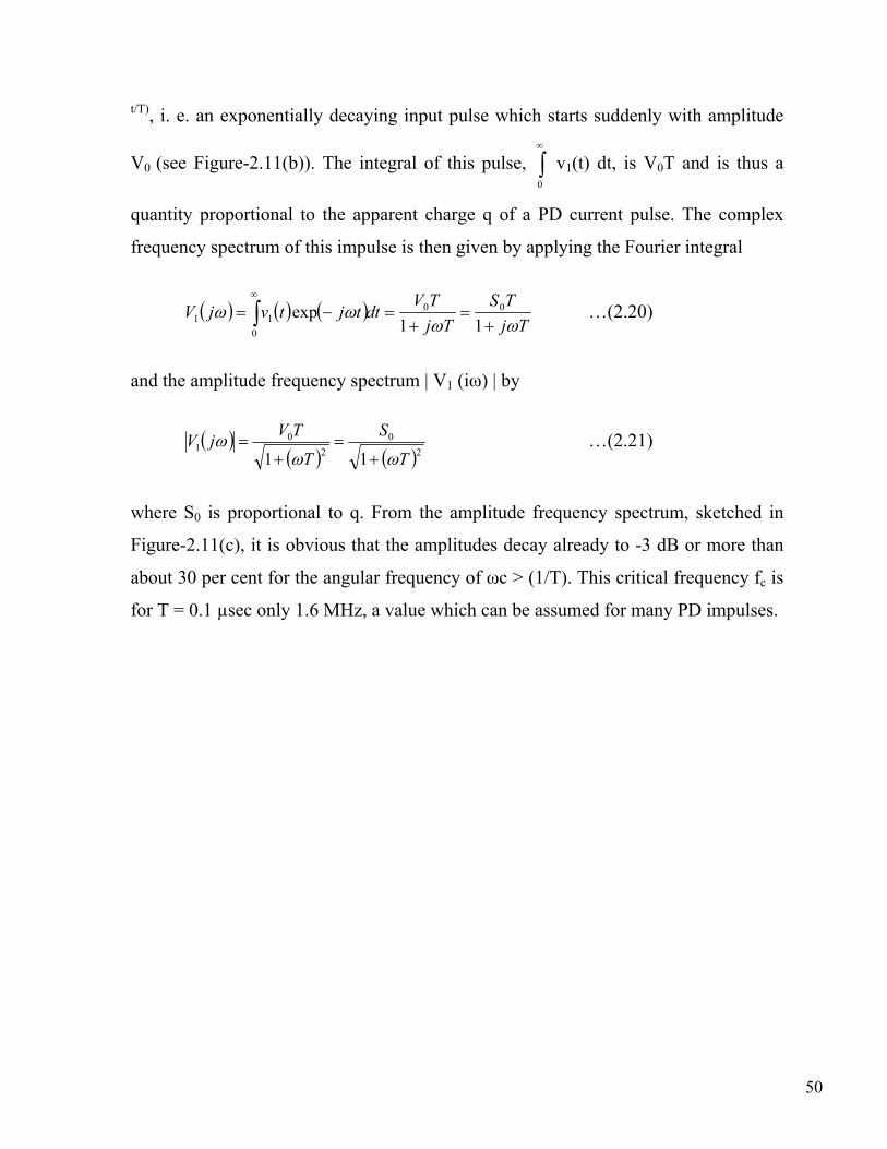
As the indication of a narrow-band instrument, if tuned to fm, will be proportional to
the relevant amplitude of this spectrum at fm, then the recommendations of the new
standard can well be understood. If the input PD current pulse were distorted by
53
oscillations, the amplitude frequency spectrum would also be distorted by maxima
and minima, which can then be recorded by tuning fm.
If the narrow-band instrument is tuned to the constant part of the spectrum which is
proportional to q, and assumed a Dirac pulse or delta function of magnitude V0T = S0
to calculate its output voltage V2(t).
As the spectrum of a Dirac pulse is constant for all frequencies, the response V2 (t) is
then proportional to S0 at any frequency fm. The impulse response of the instrument is
then of course dependent upon the exact (output/input voltage) transfer function G(jω)
of the system. However, the actual band-pass characteristic by an idealized one as
shown in Figure-2.11(d), with a mid-band angular frequency ωm, an angular
bandwidth Δω and the constant amplitude or ‘scale factor’ G0 within ωm ±(Δω/2).
For such ideal band-pass systems and especially narrow-band amplifiers the phase
shift Φ(ω) may well be assumed to be linear with frequency as indicated, at least
within the band-pass response. With this approximation no phase distortion is
assumed, and t0 (figure-2.11(d)) is equal to the delay time of the system. The impulse
response with S0 as input pulse appearing at t = 0 can then be evaluated from
( ) ( )[ ] ωωπ
ω
ω
ω
ω
dttGStvm
m
∫Δ+
Δ−
−=2/
2/
0002 cos1 …(2.22)
This integral can easily be solved; the result is
( ) ( ) ( )0000
2 cos2
ttttsiGStv m −⎥⎦⎤
⎢⎣⎡ −ΔΔ
= ωωπ
ω …(2.23)
Where si(x) = Sin (x) / x
Equation-2.15 shows an oscillating response whose main frequency is given by fm =
ωm/2π, the amplitudes are essentially given by the si(x) function, which is the
54
envelope of the oscillations. A calculated example for such a response is shown in
figure-2.11(e). The maximum value will be reached for t = t0 and is clearly given by
fGSGSV Δ=Δ
= 0000
max2 2π
ω …(2.24)
where Δf is the idealized bandwidth of the system.
Here, the two main disadvantages of narrow-band receivers can easily be seen: first,
for Δω<< ωm the positive and negative peak values of the response are equal and
therefore the polarity of the input pulse cannot be detected. The second disadvantage
is related to the long duration of the response. Although more realistic narrow band
systems will effectively avoid the response amplitudes outside of the first zero values
of the (sin x)/x function, the full length τ of the response, with τ as defined by figure-
2.11(e), becomes
( ) wf Δ=
Δ=
πτ 42 …(2.25)
In above equation τ is quite large for small values of Δf and the actual definition of
the ‘pulse resolution time Tr ’ as defined before. This quantity is about 10 % smaller
than τ, but still much larger than for wide-band PD detectors.
Simple narrow-band detectors use only RLC resonant circuits with high quality
factors Q, the resonance frequency of which cannot be tuned. Although then their
responses are still quite similar to the calculated one (equation-2.23), figure-2.12
shown such a response for a ‘double pulse’ taken from a commercial PD instrument.
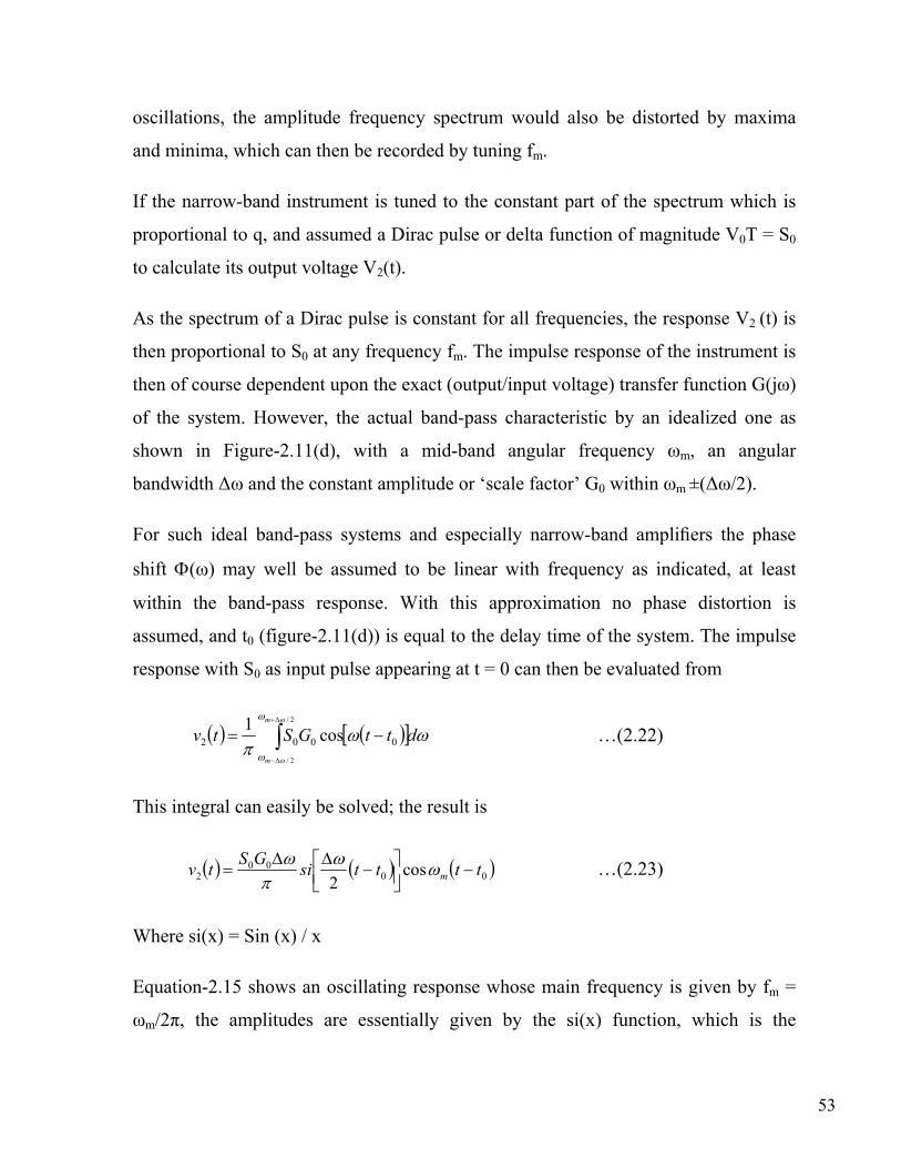
55
Figure 2.12 Response of a Simple Narrow-band Circuit with Δf = 10 kHz; fm = 75 kHz
RADIO DISTURBANCE (INTERFERENCE) METERS FOR THE DETECTION OF PD
As instruments such as those specified by the International Special Committee on
Radio Disturbance or similar organizations are still in common uses for PD detection.
The possible application of an ‘RDV’ or ‘RIV’ meter is still mentioned within the
new standard.
New types of instruments related to the CISPR Standard are often able to measure
‘radio disturbance voltages, currents and fields’ within a very large frequency range,
based on different treatment of the input quantity. Within the PD standard, however,
the expression ‘Radio Disturbance Meter’ is only applied for a specific radio
disturbance (interference) measuring apparatus, which is specified for a frequency
band of 150 kHz to 30MHz (band B) and which fulfils the requirements for a so-
called ‘quasi-peak measuring receivers’.
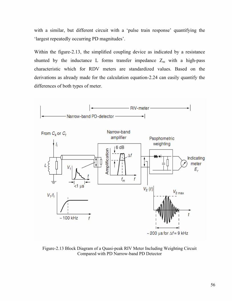
Figure-2.13 shows diagram of such a simple RIV meter, which is compared with the
principle of a narrow-band PD instrument as, described and discussed before. The
main difference is only the ‘quasi-peak’ or ‘psopho- metric weighting circuit’ that
simulates the physiological noise response of the human ear. As already mentioned
within the introduction of this section, forthcoming PD instruments will be equipped
56
with a similar, but different circuit with a ‘pulse train response’ quantifying the
‘largest repeatedly occurring PD magnitudes’.
Within the figure-2.13, the simplified coupling device as indicated by a resistance
shunted by the inductance L forms transfer impedance Zm with a high-pass
characteristic which for RDV meters are standardized values. Based on the
derivations as already made for the calculation equation-2.24 can easily quantify the
differences of both types of meter.
Figure-2.13 Block Diagram of a Quasi-peak RIV Meter Including Weighting Circuit Compared with PD Narrow-band PD Detector
57
The quasi-peak RDV meters are designed with a very accurately defined overall pass-
band characteristic fixed at Δf = 9 kHz. They are calibrated in such a way that the
response to Dirac type of equidistant input pulses providing each a volt–time area of
0.316 µVs at a pulse repetition frequency (N) of 100Hz. This is equal to an
unmodulated sine-wave signal at the tuned frequency having an e.m.f. of 2mV r.m.s.
as taken from a signal generator driving the same output impedance as the pulse
generator and the input impedance of the RIV meter.
By this procedure the impulse voltages as well as the sine-wave signal are halved. As
for this repetition frequency of 100Hz the calibration point shall be only 50 per cent
of V2max in eqn. (2.16), the relevant reading of the RDV meter will be
22
221 00
00fGSfGSERDV
Δ=Δ= …(2.26)
As G0 = 1 for a proper calibration and Δf = 9kHz, S0 = 158 µVs, the indicated
quantity is S0Δf/√2= 1mV or 60dB (µV), as the usual reference quantity is 1 µV. RDV
meters are thus often called ‘microvolt meters’.
This response is now weighted by the ‘quasi-peak measuring circuit’ with a specified
electrical charging time constant τ1= 1ms, an electrical discharging time constant τ2 =
160 ms and by an output voltmeter, which, for conventional instruments, is of moving
coil type, critically damped and having a mechanical time constant τ3 = 160ms.
58
Figure-2.14 Variation of CISPR Radio Interference Meter Reading with Repetition Frequency N, for Constant Input Pulses
This procedure makes the reading of the output voltmeter dependent on the pulse
repetition frequency N. This non-linear function f(N) is shown in figure-2.14 and is
only accurate if the input pulses are equidistant and of equal amplitudes. It can be
seen that for N > 1000 the function f(N) would saturate to a value of 2, for which,
however, superposition errors occur.
With this function f(N) we can now finalize the reading of an RIV meter by taking the
transfer impedance Zm of CD in eqn (2.18) into account, which converts input PD
currents into input voltages v1(t). For RDV meters, this transfer impedance, the real
value of which |Zm| is constant for the frequency range under consideration, the
quantity S0 in eqn. (2.18) may then be written as,
( ) ( ) qZdttiZdttvS mm === ∫ ∫ 110 …(2.27)
Where q is the measured charge quantity for an impulse current i1(t). Here, eq-2.18
can be rewritten as )(2
NfZfqGoE mRDV Δ= and conversion factors between the
59
measured charge q and the indicated voltage by an RDV meter can be calculated. For
N = 100 equidistant pulses of equal magnitude f(N)= 1, Δf = 9 kHz, correct
calibration G0 = 1 and a reading of 1mV (ERDV) or 60 dB, charge magnitudes of 1 nC
for | Zm | = 150 (or 60) Ω can be calculated. These relationships have also been
confirmed experimentally. Instead of eqn (2.19) the new standard displays.
URDV ( )( ) /m iq fZ f N k= Δ …(2.28)
where
N = pulse repetition frequency,
f(N) = the non-linear function of N (see figure-2.14),
Δf = instrument bandwidth (at 6 dB),
Zm = value of a purely resistive measuring input impedance of the instrument,
ki = the scale factor for the instrument (= q / URDV)
As the weighting of the PD pulses is different for narrow-band PD instruments and
quasi-peak RDV meters, there is no generally applicable conversion factor between
readings of the two instruments. The application of RDV meters is thus not forbidden;
but if applied the records of the tests should include the readings obtained in
microvolt and the determined apparent charge in pico coulombs together with relevant
information concerning their determination.
ULTRA-WIDE-BAND INSTRUMENTS FOR PD DETECTION
The measurement of PD current pulses belongs to this kind of PD detection as well as
any similar electrical method to quantify the intensity of PD activities within a test
object. Such methods need coupling devices with high-pass characteristics which
shall have a pass band up to frequencies of some 100MHz or even higher.
60
Records of the PD events are then taken by oscilloscopes, transient digitizers or
frequency selective voltmeters especially spectrum analyzers. For the location of
isolated voids with partial discharges in cables a bandwidth of about some 10MHz
only is useful, whereas tests on GIS (gas-insulated substations or apparatus)
measuring systems with ‘very high’ or even ‘ultra-high’ frequencies (VHF or UHF
methods for PD detection) can be applied.
The development of any partial discharge in sulphur hexafluoride is of extremely
short duration providing significant amplitude frequency spectra up to the GHz
region. More information concerning this technique can be found in the literature..
As none of these methods provides integration capabilities, they cannot quantify
apparent charge magnitudes, but may well be used as a diagnostic tool.
61
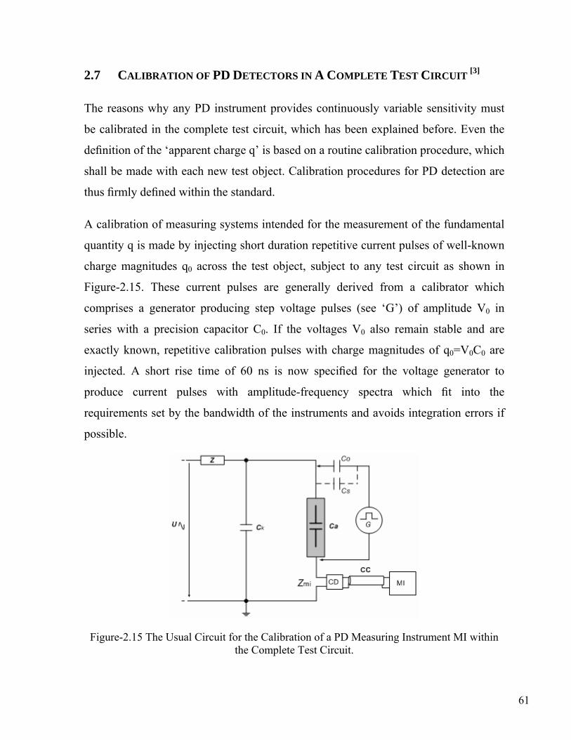
2.7 CALIBRATION OF PD DETECTORS IN A COMPLETE TEST CIRCUIT [3]
The reasons why any PD instrument provides continuously variable sensitivity must
be calibrated in the complete test circuit, which has been explained before. Even the
definition of the ‘apparent charge q’ is based on a routine calibration procedure, which
shall be made with each new test object. Calibration procedures for PD detection are
thus firmly defined within the standard.
A calibration of measuring systems intended for the measurement of the fundamental
quantity q is made by injecting short duration repetitive current pulses of well-known
charge magnitudes q0 across the test object, subject to any test circuit as shown in
Figure-2.15. These current pulses are generally derived from a calibrator which
comprises a generator producing step voltage pulses (see ‘G’) of amplitude V0 in
series with a precision capacitor C0. If the voltages V0 also remain stable and are
exactly known, repetitive calibration pulses with charge magnitudes of q0=V0C0 are
injected. A short rise time of 60 ns is now specified for the voltage generator to
produce current pulses with amplitude-frequency spectra which fit into the
requirements set by the bandwidth of the instruments and avoids integration errors if
possible.
Figure-2.15 The Usual Circuit for the Calibration of a PD Measuring Instrument MI within the Complete Test Circuit.
62
Whereas further details for the calibration procedures are not discussed here, the new
philosophy in reducing measuring errors during PD tests will be presented. It has been
known for some time that measuring uncertainties in PD measurements are large.
Even today PD tests on identical test objects performed with different types of
commercially available systems will provide different results after routine calibration
performed with the same calibrator.
The main reasons for this uncertainty are the different transfer impedances
(bandwidth) of the measuring systems, which up to 1999 have never been well
defined and quantified. The new but not very stringent requirements related to this
property will improve the situation; together with other difficulties related to
disturbance levels, measures uncertainties of more than about 10 per cent (if exists).
The most essential part of the new philosophy concerns the calibrators, for which – up
to now – no requirements for their performance exists.
Tests on daily used commercial calibrators sometime display deviations of more than
10 per cent of their nominal values. Therefore routine type and performance tests on
calibrators have been introduced with the new standard. At least the first of otherwise
periodic performance tests should be traceable to national standards, this means they
shall be performed by any accredited calibration laboratory. With the introduction of
this requirement it can be assumed that the uncertainty of the calibrator charge
magnitudes q0 can be assessed to remain within ±5 per cent or 1 pC, whichever is
greater, from its nominal values. Very recently executed inter-comparison tests on
calibrators performed by accredited calibration laboratories showed that impulse
charges could be measured with an uncertainty of about 3 per cent.
63
2. 8 DIGITAL INSTRUMENTS FOR PD MEASUREMENTS [2]
Between 1970 and 1980 the state of the art in computer technology and related
techniques rendered the first application of digital acquisition and processing of
partial discharge magnitudes. Since then this technology was applied in numerous
investigations generally made with either instrumentation set up with available
components or some commercial instruments equipped with digital techniques.
One task for the working group evaluating the new IEC Standard concerned with
implementation of few key requirements for this technology. It is again not the aim of
this section to go into details of digital PD instruments, as too many variations in
designing such instruments exist.
In general, digital PD instruments are based on analogue measuring systems or
instruments for the measurement of the apparent charge q followed by a digital
acquisition and processing system. These digital parts of the system are then used to
process analogue signals for further evaluation, to store relevant quantities and to
display test results.
It is possible that in the near future a digital PD instrument may also be based on a
high-pass coupling device and a digital acquisition system without the analogue signal
processing front end. The availability of cheap but extremely fast flash A/D
converters and digital signal processors (DSPs) performing signal integration is a
prerequisite for such solutions.
The main objective of applying digital techniques to PD measurements is based on
recording in real time and most of consecutive PD pulses are within a voltage cycle of
the test voltage. These PD pulses are quantified by its apparent charge qi (occurring at
time instant ti) and its instantaneous values of the test voltage ui (occurring at this
time instant ti) or for alternating voltages, at phase angle of Φi
64
As, however, the quality of hardware and software used may limit the accuracy and
resolution of the measurement of these parameters, the new standard provides some
recommendations and requirements which are relevant for capturing and registration
of the discharge sequences. One of the main problems in capturing the output signals
from the analogue front end correctly can be seen from Figures-2.12 and Figure-2.14
respectively, in which three output signals of two consecutive PD events are shown.
Although none of the signals is distorted by superposition errors, several peaks of
each signal with different polarities are present. For the wideband signals, only the
first peak value shall be captured and recorded including polarity, which is not easy to
do. For the narrow-band response for which polarity determination is not necessary,
only the largest peak is proportional to the apparent charge.
For both types of signals therefore only one peak value shall be quantified, recorded
and stored within the pulse resolution time of the analogue measuring system.
Additional errors can well be introduced by capturing wrong peak values, which add
to the errors of the analogue front end.
Further study of PD instruments is related to post-processing of the recorded values.
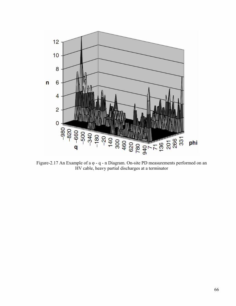
Firstly; the so-called ‘φi - qi - ni’ patterns, available from the recorded and stored data
in which ni is the number of identical or similar PD magnitudes recorded within short
time (or phase) intervals and an adequate total recording duration can be used to
identify and localize the origin of the PDs based on earlier experience and/or even to
establish physical models for specific PD processes. If recorded raw data are too much
obscured by disturbances, quite different numerical methods may also be applied for
disturbance level reduction.
This chapter concludes with two records of results from PD tests made with digital
PD instrument. Figure-2.16 and figure-2.17, individually, shows typical test results of
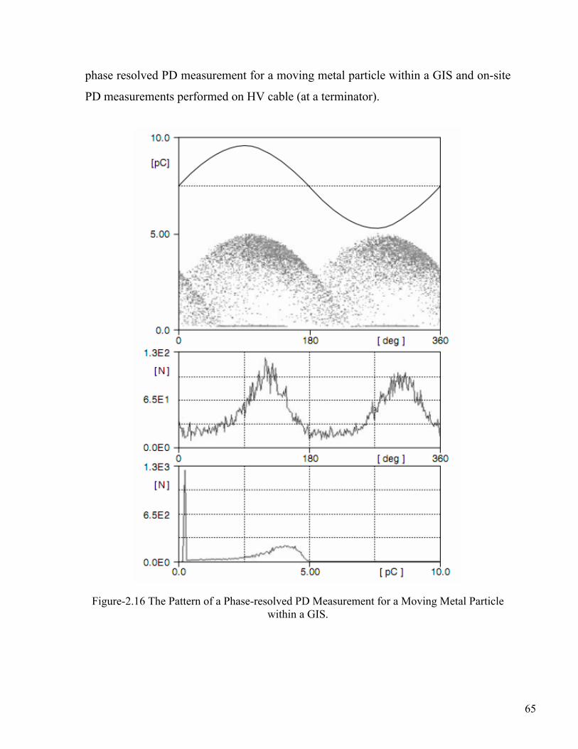
65
phase resolved PD measurement for a moving metal particle within a GIS and on-site
PD measurements performed on HV cable (at a terminator).
Figure-2.16 The Pattern of a Phase-resolved PD Measurement for a Moving Metal Particle within a GIS.
66
Figure-2.17 An Example of a φ - q - n Diagram. On-site PD measurements performed on an HV cable, heavy partial discharges at a terminator
67
2.9 SOURCE OF INTERFERENCE AND REDUCTION OF DISTURBANCES [2, 3]
One of the most difficult problems that must be coped with in making PD
measurements is that of electrical interference (noise) which falls into following
categories:
• Disturbances, which occur if test circuit is not energized. They may be caused
by switching operations in other circuits, commuting machines, high voltage
tests in the vicinity radio transmission etc.
• Disturbances which only occur when the test circuit is energized but which
don’t occur in the test object, for e.g. PD in testing transformer, HV
conductors, bushings, disturbances caused by sparking of imperfectly earthed
objects in the vicinity or the loose connections in the area of high voltages.
• Disturbances which may also caused by higher harmonics of test voltage
within the band-width of the measuring instruments. These disturbances
usually increase with increasing the voltage.
These disturbances can seriously affect the sensitivity of the test circuit and must be
controlled and suppressed to minimum and to use detectors equipped with an
oscilloscope to give the maximum opportunity for distinguishing spurious signals
from the discharges in the test sample.
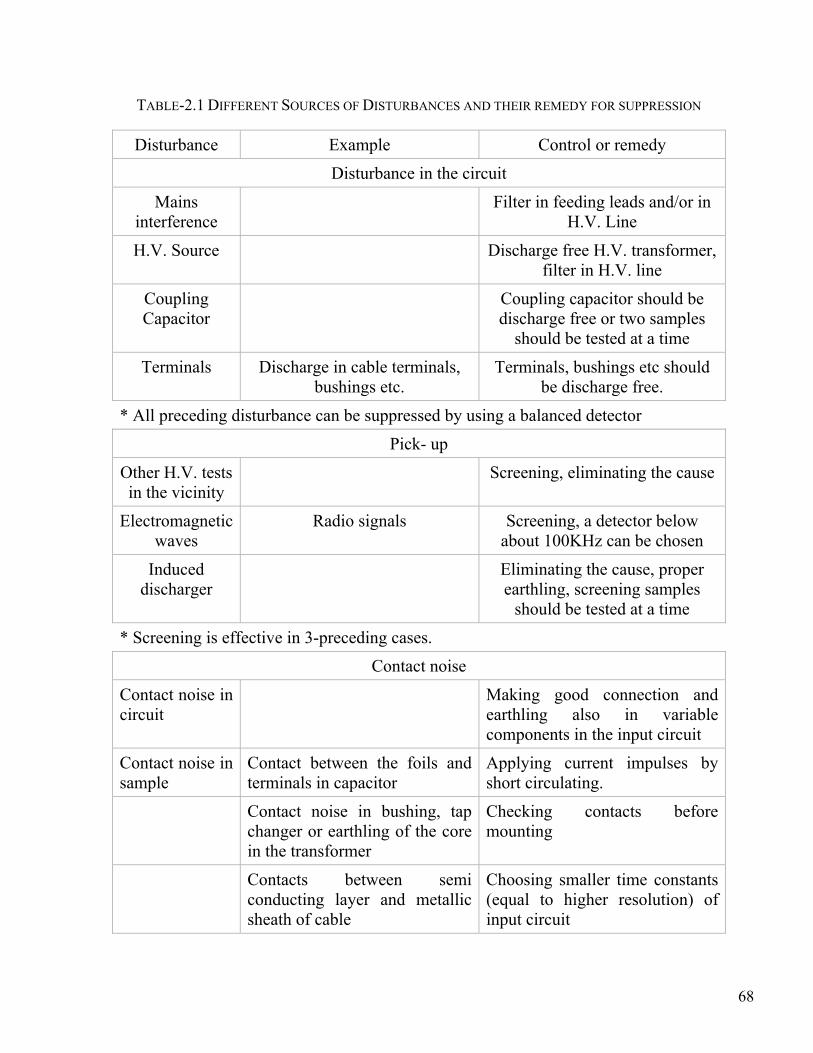
The following table gives the complete account of different sources of disturbances
and their control or remedy for suppression.
All preceding disturbances can be suppressed by using a balance detection method.
68
TABLE-2.1 DIFFERENT SOURCES OF DISTURBANCES AND THEIR REMEDY FOR SUPPRESSION
Disturbance Example Control or remedy
Disturbance in the circuit
Mains interference
Filter in feeding leads and/or in H.V. Line
H.V. Source Discharge free H.V. transformer, filter in H.V. line
Coupling Capacitor
Coupling capacitor should be discharge free or two samples
should be tested at a time
Terminals Discharge in cable terminals, bushings etc.
Terminals, bushings etc should be discharge free.
* All preceding disturbance can be suppressed by using a balanced detector
Pick- up
Other H.V. tests in the vicinity
Screening, eliminating the cause
Electromagnetic waves
Radio signals Screening, a detector below about 100KHz can be chosen
Induced discharger
Eliminating the cause, proper earthling, screening samples
should be tested at a time
* Screening is effective in 3-preceding cases.
Contact noise
Contact noise in circuit
Making good connection and earthling also in variable components in the input circuit
Contact noise in sample
Contact between the foils and terminals in capacitor
Applying current impulses by short circulating.
Contact noise in bushing, tap changer or earthling of the core in the transformer
Checking contacts before mounting
Contacts between semi conducting layer and metallic sheath of cable
Choosing smaller time constants (equal to higher resolution) of input circuit
69
It is obvious that up to now numerous methods to reduce disturbances have been and
still are a topic for research and development, which can only be mentioned and
summarized here.
The most efficient method to reduce disturbances is screening and filtering, in general
only possible for tests within a shielded laboratory where all electrical connections
running into the room are equipped with filters. This method is expensive, but
inevitable if sensitive measurements are required, i.e. if the PD magnitudes as
specified for the test objects are small, e.g. for HV cables.
Straight PD-detection circuits as already shown in Figure-2.6 are very sensitive to
disturbances: any discharge within the entire circuit, including HV source, which is
not generated in the test specimen itself, will be detected by the coupling device CD.
Therefore, such ‘external’ disturbances are not rejected. Independent of screening and
filtering mentioned above, the testing transformer itself should be PD free as far as
possible, as HV filters or inductors indicated in figure-2.6 are expensive. It is also
difficult to avoid any partial discharges at the HV leads of the test circuit, if the test
voltages are very high. A basic improvement of the straight detection circuit may
therefore become necessary by applying a ‘balanced circuit’, which is similar to a
Schering bridge.
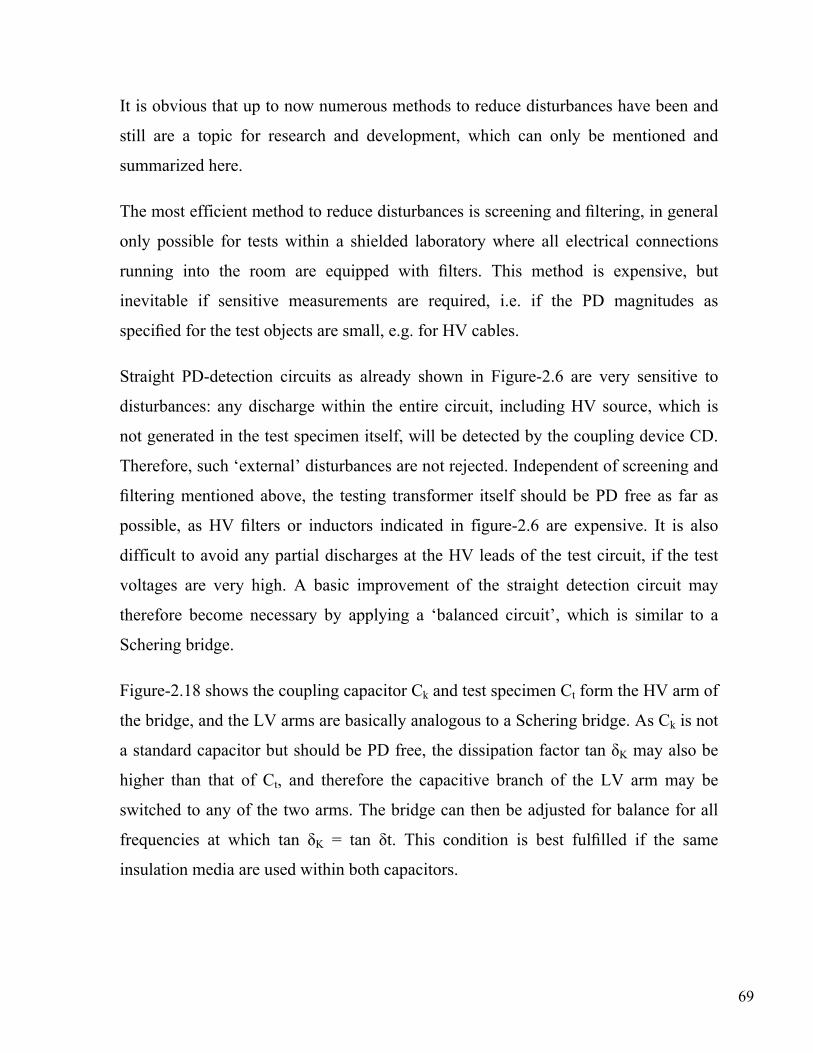
Figure-2.18 shows the coupling capacitor Ck and test specimen Ct form the HV arm of
the bridge, and the LV arms are basically analogous to a Schering bridge. As Ck is not
a standard capacitor but should be PD free, the dissipation factor tan δK may also be
higher than that of Ct, and therefore the capacitive branch of the LV arm may be
switched to any of the two arms. The bridge can then be adjusted for balance for all
frequencies at which tan δK = tan δt. This condition is best fulfilled if the same
insulation media are used within both capacitors.
70
The use of a partial discharge-free sample for Ck of the same type as used in Ct is thus
advantageous. If the frequency dependence of the dissipation factors is different in the
two capacitors, a complete balance within a larger frequency range is not possible.
Nevertheless, a fairly good balance can be reached and therefore most of the
sinusoidal or transient voltages appearing at the input ends of Ck and Ct cancel out
between the points 1 and 2. A discharge within the test specimen, however, will
contribute to voltages of opposite polarity across the LV arms, as the PD current is
flowing in opposite directions within Ck and Ct.
Polarity discrimination methods take advantage of the effect of opposite polarities of
PD pulses within both arms of a PD test circuit.
Figure-2.18 Differential PD bridge (Balanced Circuit)
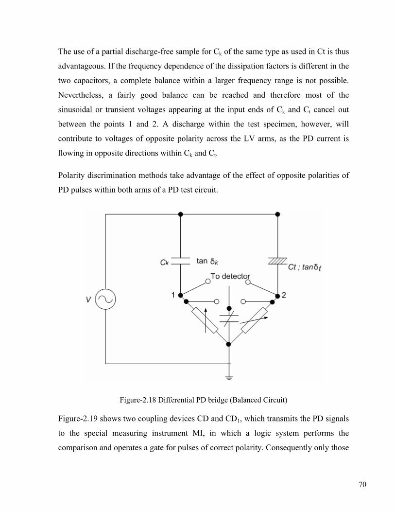
Figure-2.19 shows two coupling devices CD and CD1, which transmits the PD signals
to the special measuring instrument MI, in which a logic system performs the
comparison and operates a gate for pulses of correct polarity. Consequently only those
71
PD pulses which originate from the test object are recorded and quantified. This
method was proposed by I.A. Black.
Figure-2.19 Polarity Discrimination Circuit
Another extensively used method is the time window method to suppress interference
pulses. All kinds of instruments may be equipped with an electronic gate, which can
be opened and closed at preselected moments, thus either passing the input signal or
blocking it. If the disturbances occur during regular intervals the gate can be closed
during these intervals. In tests with alternating voltage, the real discharge signals often
occur only at regularly repeated intervals during the cycles of test voltage. The time
window can be phase locked to open the gate only at these intervals.
Some more sophisticated methods are used for digital acquisition of partial discharge
quantities.
72
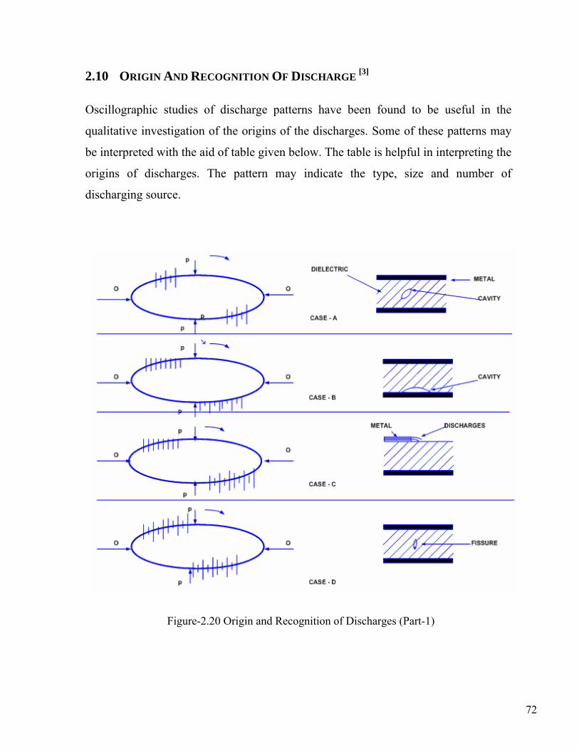
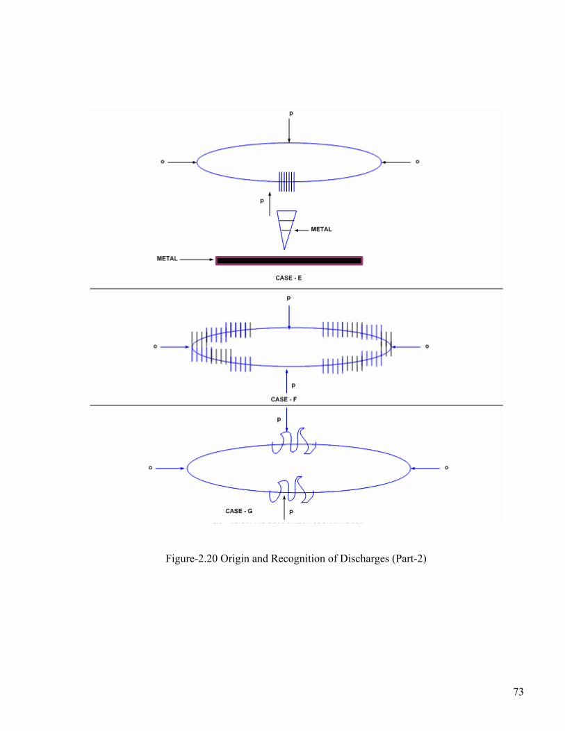
2.10 ORIGIN AND RECOGNITION OF DISCHARGE [3]
Oscillographic studies of discharge patterns have been found to be useful in the
qualitative investigation of the origins of the discharges. Some of these patterns may
be interpreted with the aid of table given below. The table is helpful in interpreting the
origins of discharges. The pattern may indicate the type, size and number of
discharging source.
Figure-2.20 Origin and Recognition of Discharges (Part-1)
73
Figure-2.20 Origin and Recognition of Discharges (Part-2)
74
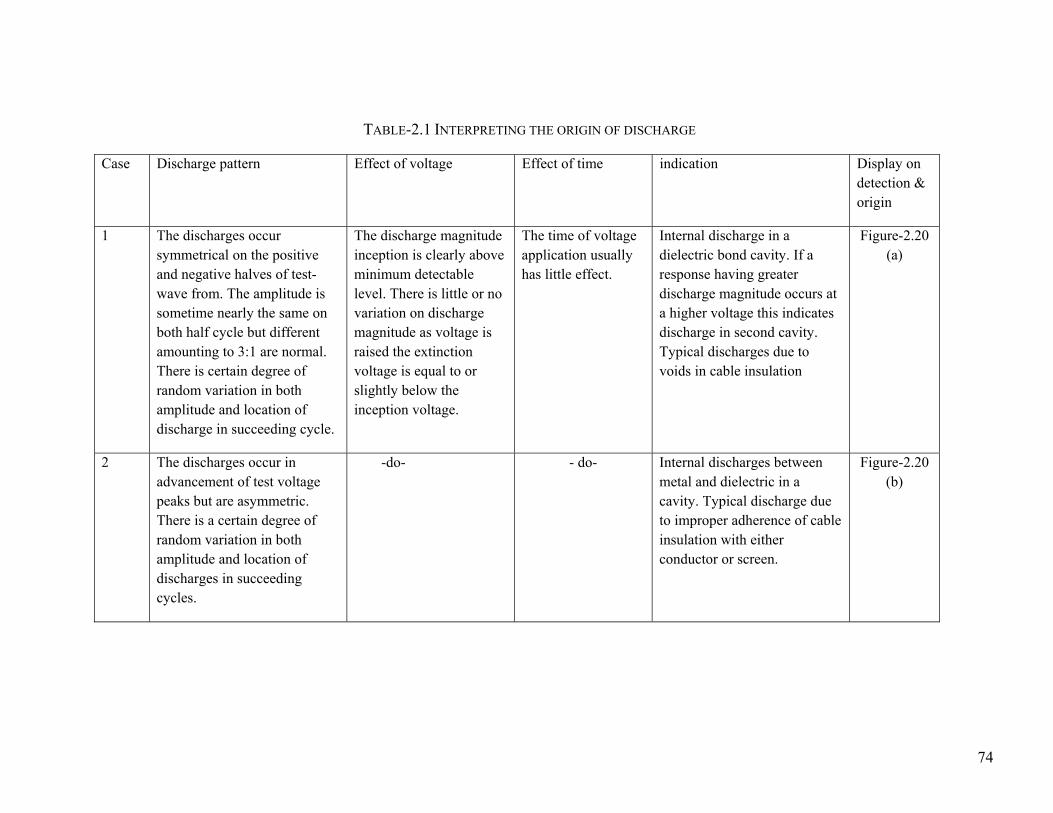
TABLE-2.1 INTERPRETING THE ORIGIN OF DISCHARGE
Case Discharge pattern Effect of voltage Effect of time indication Display on detection & origin
1 The discharges occur symmetrical on the positive and negative halves of test-wave from. The amplitude is sometime nearly the same on both half cycle but different amounting to 3:1 are normal. There is certain degree of random variation in both amplitude and location of discharge in succeeding cycle.
The discharge magnitude inception is clearly above minimum detectable level. There is little or no variation on discharge magnitude as voltage is raised the extinction voltage is equal to or slightly below the inception voltage.
The time of voltage application usually has little effect.
Internal discharge in a dielectric bond cavity. If a response having greater discharge magnitude occurs at a higher voltage this indicates discharge in second cavity. Typical discharges due to voids in cable insulation
Figure-2.20 (a)
2 The discharges occur in advancement of test voltage peaks but are asymmetric. There is a certain degree of random variation in both amplitude and location of discharges in succeeding cycles.
-do- - do- Internal discharges between metal and dielectric in a cavity. Typical discharge due to improper adherence of cable insulation with either conductor or screen.
Figure-2.20 (b)

75
Case Discharge pattern Effect of voltage Effect of time indication Display on detection & origin
3 Same as case II except that the number of discharges increase with test voltage.
Same as above except that the discharge magnitude increase steadily as voltage is raised above inception.
-do- Surface discharges talking place between external metal and dielectric surface typical discharges due to improper end terminations of a cable.
Figure-2.20 (c)
4 Similar as case I response. If the voltage is raised to its maximum value, then quickly lowered, the characteristic is similar to for cable I discharge.
The discharge magnitude falls with time but the extinction voltage becomes higher.
The behavior describe has been found in cable insulation containing a cavity in form of fissure in the direction of electric field.
Figure-2.20 (d)
5 The discharge occur on one half cycle of the test wave form only asymmetrically disposed about the voltage peak and all of them are equal in magnitude and are equally spaced in time.
There is no change in discharge magnitude as the voltage is raised and the magnitude remains constant as the voltage lowered. The extinction voltage coincides with inception voltage
The response is normally unaffected by the time for which the test voltage is applied.
External corona discharge from sharp metal points.
Figure-2.20 (e)

76
Case Discharge pattern Effect of voltage Effect of time indication Display on detection & origin
6 Coarse and irregular usually unresolved symmetrically distributed about test voltage zeros, but the amplitude is zero near the test voltage peaks.
The magnitude usually increases slowly and proportionally with voltage. It is also observed that it may disappear completely at a particular voltage level and be absent for all voltages above that level.
The response is normally unaffected by the time for which the test voltage is applied.
Contact noise due to imperfect metal to metal joints.
Figure-2.20 (f)
7 Groups of low frequency oscillations located on the test voltages peaks.
The response is usually undetectable in lower range of voltage &grows rapidly as voltage approaches highest rated voltage of the test transformer
-do- Harmonics generated by test transformer core.
Figure-2.20 (g)