Embed Size (px)
Citation preview
14
CHAPTER 2
CLASS E POWER AMPLIFIERS AND ITS
LINEARIZATION
2.1 INTRODUCTION
To improve the performance of wireless systems, Amplifiers
operated in the Radio Frequency (RF) band are used both in the wireless
transmitter and receiver. Power amplifiers (PAs) are used in the transmitter to
enable power amplification of baseband signals. The selection of PAs for the
transmitter is based on the efficiency, Device Utilization Factor (DUF) and
linearity of the amplifier. The DUF is very low for Class E PA than the other
PAs. To achieve high efficiency, Class E power amplifiers are preferred.
Class E PAs operate with power losses lesser than class B or class C
amplifiers. They can be constructed with Silicon or Gallium Arsenide
semiconductors in CMOS technology. Class E PAs can be designed for
narrowband operations and give maximum output power for 50% duty cycle.
High power amplifiers in the base stations and the repeaters for wireless
systems need extremely high linearity. In Class E PAs, the effect of
components and frequency variations are small since the MOSFET device is
operated in switching mode. But the drawback of Class E PAs is the
nonlinearity of the amplifier. This drawback can be improved by linearization
techniques like analog Predistortion, digital Predistortion, feed forward
Predistortion etc. In this thesis, an attempt is made to linearize the PAs using
Analog Predistortion method.
15
In this chapter, Power amplifiers operating with center frequency of
947.5MHz and 2.4GHz which can be used for the transmitter in beamforming
systems are proposed. The PAs implemented provide high Power Added
Efficiency (PAE) and low Noise Figure (NF). The linearity of the power
amplifiers is improved by using Square law and Cubic law Analog
Predistortion techniques. The PAs implemented provide high SNR and the
linearity is improved by suppressing the power in the 2nd
and 3rd
order
harmonics. The power amplifiers are designed and implemented using
0.35µm CMOS technology in Advanced Design System (ADS). The results
of the proposed PAs are compared with those of the existing PAs.
2.2 LITERATURE SURVEY
There are several literature available on the design of Class E PAs.
The Class E Power Amplifier (PA) was described initially by Nathan Sokal et
al (1975) using Bipolar Junction Transistor (BJT) as switching device. The
design equations and advantages of Class E PAs using BJT are proposed by
Nathan Sokal et al (2001). Design of Power Amplifiers at 2.4GHz/900MHz
and Implementation of On-chip Linearization Technique in 0.18/0.25µm
CMOS proposed by Padmanava Sen et al (2004) uses class AB power
amplifier and the efficiency is only 20%. An Error Vector Magnitude (EVM)-
optimized Power Amplifier for 2.4GHz WLAN Application proposed by
Michael Sagebiel et al (2005) provides a PAE of 42%. A reconfigurable
CMOS power amplifier operating from 0.9 to 2.4 GHz for Wireless
application proposed by Seok-Oh Yun and Hyung-Joun yoo (2006) provides a
PAE of 42 to 57%. The design flow for CMOS based Class E and Class F
PAs is proposed by Mladen Bozanic and Saurabh Sinha (2009). As existing
PAs have low efficiency there is a need for power amplifiers with high PAE
in many wireless applications.
16
The linearity of PAs can be improved by linearization techniques
like Analog Predistortion, Digital predistortion, feed forward, Cartesian
feedback etc. Analog Predistortion for high power RF amplifiers is proposed
by Timo Rahkonen et al (1999) for Class A, Class B and Class C power
amplifiers. Power amplifiers working with Lateral Diffusion MOS (LDMOS)
is proposed by Jaehyok Yi et al (2000). Seung-Yup Lee et al (2004) has
proposed Independently Controllable 3rd
order and 5th
Order Analog
Predistortion for power amplifiers and the second order distortions are not
considered. Optimization of adaptive cubic predistorter for multi level
Quadrature Amplitude Modulation is proposed by Bernardini et al (1991) for
Amplifiers using Travelling Wave Tubes. In the Genetic algorithm
optimization of a hybrid analog/digital predistorter for RF power amplifiers
proposed by Cebrail Ciftlikli et al (2007) the circuit complexity is more due to
ADC and DAC in the circuit. The second order distortions are very low or
zero when low frequency analysis is performed for a circuit. When high
frequency analysis is performed the 2nd
order distortions are high as specified
by Bosco Leung (2002). Linearization has to be performed not only to reduce
3rd
order and 5th
order distortion but also to remove the second order
distortions.
2.3 CMOS POWER AMPLIFIERS
Power amplifiers are designed to work with high efficiency using
active devices like BJT, FET and MOSFET. There is a major loss of power in
these amplifiers due to power dissipation in the output active devices.
Therefore care has to be taken to minimize the power dissipation in power
amplifiers designed to work at high frequencies. To reduce the power
dissipation, the voltage across the device can be minimized when current
flows or the current through the device can be minimized when voltage exists
across it. Power amplifiers are generally classified as switching and non-
17
switching. Class A, Class B and Class C PAs are non-switching amplifiers in
which the MOSFET is operated as a dependent current source. The drawback
of these amplifiers is that their efficiency is low.
In Class D, Class E, Class F and Class S PAs which use MOSFET
as a switch, the efficiency is 100%, theoretically. In switching amplifiers
Class-E has maximum efficiency, minimum DUF and the power dissipation
will be low. Hence the implementation of Class E PAs is considered in this
thesis. Efficiency is maximized in the amplifier by minimizing power
dissipation, while providing a desired output power. The comparison of
different classes of power amplifiers discussed by Marian Kazimierczuk
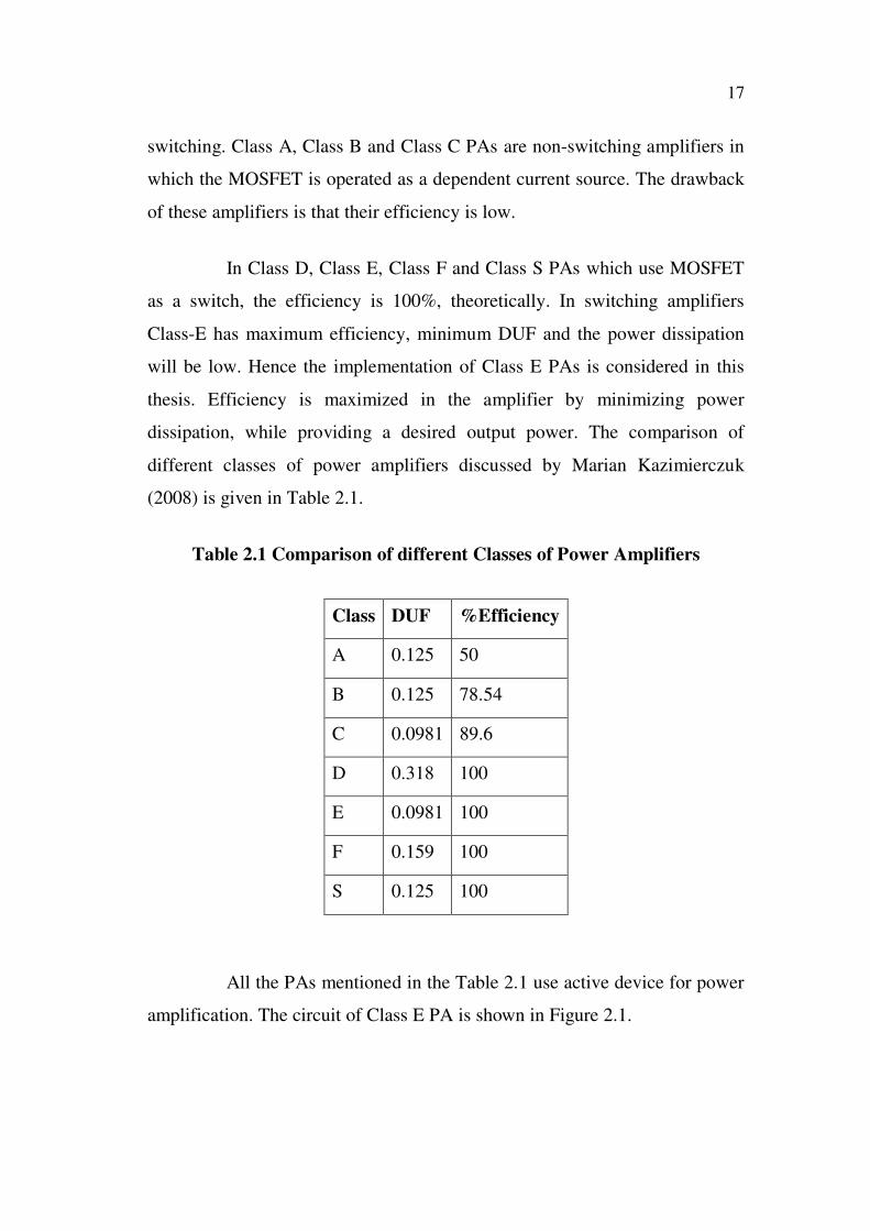
(2008) is given in Table 2.1.
Table 2.1 Comparison of different Classes of Power Amplifiers
Class DUF %Efficiency
A 0.125 50
B 0.125 78.54
C 0.0981 89.6
D 0.318 100
E 0.0981 100
F 0.159 100
S 0.125 100
All the PAs mentioned in the Table 2.1 use active device for power
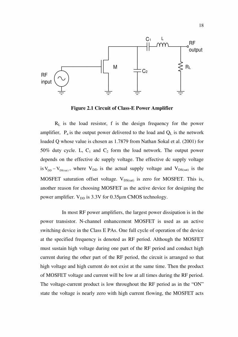
amplification. The circuit of Class E PA is shown in Figure 2.1.
18
LC1
C2RLM
RF
output
RF
input
Figure 2.1 Circuit of Class-E Power Amplifier
RL is the load resistor, f is the design frequency for the power
amplifier, Pa is the output power delivered to the load and QL is the network
loaded Q whose value is chosen as 1.7879 from Nathan Sokal et al. (2001) for
50% duty cycle. L, C1 and C2 form the load network. The output power
depends on the effective dc supply voltage. The effective dc supply voltage
is DS(DD sat)V V , where VDD is the actual supply voltage and VDS(sat) is the
MOSFET saturation offset voltage. VDS(sat) is zero for MOSFET. This is,
another reason for choosing MOSFET as the active device for designing the
power amplifier. VDD is 3.3V for 0.35µm CMOS technology.
In most RF power amplifiers, the largest power dissipation is in the
power transistor. N-channel enhancement MOSFET is used as an active
switching device in the Class E PAs. One full cycle of operation of the device
at the specified frequency is denoted as RF period. Although the MOSFET
must sustain high voltage during one part of the RF period and conduct high
current during the other part of the RF period, the circuit is arranged so that
high voltage and high current do not exist at the same time. Then the product
of MOSFET voltage and current will be low at all times during the RF period.
The voltage-current product is low throughout the RF period as in the “ON”
state the voltage is nearly zero with high current flowing, the MOSFET acts
19
as a low resistance closed switch. During the “OFF” state the current is zero
with high voltage, the MOSFET acts as an open switch. MOSFET as switch
is highly efficient as the “ON” and “OFF” states of the switch fulfills the
minimum voltage and minimum current requirements.
The advantage of having MOSFET is that, the oxide layer between
the gate and the channel prevents DC current from flowing through the gate.
This reduces power consumption and gives very large input impedance,
which enhances the digital switching. The insulating oxide between the gate
and channel effectively isolates a MOSFET in one logic stage from earlier
and later stages, which allows a single MOSFET output to drive a
considerable number of MOSFET inputs. This isolation makes it easier to
ignore to some extent loading effects between logic stages independently.
MOSFET provides maximum power output capability (cp) and allow a single
MOSFET to function as a switch. As the output power capability cp increases,
the maximum output power PO(max) also increases. The maximum output
power PO(max) of an amplifier with a transistor having the maximum ratings of
drain current IDM and drain to source voltage VDSM is
O(max) p DM DSMP c I V (2.1)
Class E amplifiers operating at center frequency of 947.5MHz and
2.4GHz are presented. The Power Amplifier1 (PA1) at center frequency of
947.5MHz is suitable for beamforming systems at the transmitter of the base
station in 935-960MHz band and the Power Amplifier2 (PA2) at center
frequency of 2.4GHz is suitable for beamforming systems at the transmitter of
wireless systems operating with bandwidth in the range of 2390-2410MHz
with bandwidth of 20MHz. The PAs are implemented using 0.35µm CMOS
technology.
20
The maximum frequency that the 0.35µm CMOS technology can
support is given in terms of unity-gain frequency (fT) as given by Hassan
Hassan et al (2006). Unity-gain frequency of N-channel MOSFET (NMOS)
used for the design of PA using 0.35µm CMOS technology is the frequency at
which the current gain of the MOSFET is unity. The unity-gain frequency for
this NMOS is found using AC simulation. In the AC simulation the operating
point of NMOS device is selected to be 2.5V for both VGS and VDS, saturated
with a significant overdrive voltage in order to minimize the non-quasi static
(NQS) effects.
The majority of MOSFET models implemented in SPICE are based
upon quasi static (QS) approximations. QS operation assumes that the
terminal voltages vary slowly enough for the channel charge of the MOS
transistor to achieve equilibrium instantaneously as given by Ananda Roy et
al (2003). Thus, these charges can be determined using equivalent DC
voltages applied to the terminals. At high-frequencies however, these
approximations begin to breakdown, leading to unpredictable transistor
behavior. The criteria for the onset of non-quasistatic (NQS) effects based
upon transient behavioral simulations have been proposed by Elmar Gondro
et al (2001) and Allen Ng et al (2002). These simulation results suggest that
the total inversion charge, when stimulated by a sinusoidal input voltage,
deviates from that predicted by the QS model in both amplitude and phase at
sufficiently high frequency. Results presented by Elmar Gondro et al (2001)
demonstrate that the amplitude remains nearly constant until a certain
frequency limit, while the phase shift varies linearly with phase. Using these
results, the non-quasistatic onset frequency limit fNQS can be defined
separately in terms of acceptable inversion layer amplitude and phase
deviation from that of the QS model. The amplitude is found to be minimal
until nearly the unity-gain frequency fT of the devices simulated in both Elmar
21
Gondro et al (2001) and Allen Ng et al (2002). Phase deviation was indicated
to range from ~3º at 20% of fT to ~12º at fT.
The operating point is selected to allow for sizable signal without
any clipping. The DC operating point has a direct effect upon a transistor's
cutoff frequency. A larger DC drain current will directly increase the device
transconductance, thereby directly increasing the cutoff frequency as given in
(2.2).
mT
g gb gso gdo
g1f
2 C
Iout
I Ci C Cn (2.2)
where gm is the fundamental device transconductance; Cg, Cgb, Cgso, and Cgdo
are the intrinsic input capacitance, the gate-to-bulk capacitance, the gate-to
source overlap capacitance, and the gate-to-drain overlap capacitances,
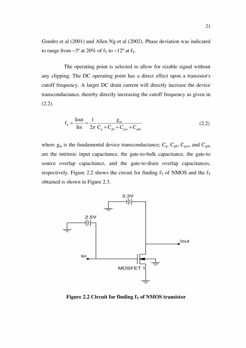
respectively. Figure 2.2 shows the circuit for finding fT of NMOS and the fT
obtained is shown in Figure 2.3.
MOSFET 1
3.3V
2.5V
Iin
Iout
Figure 2.2 Circuit for finding fT of NMOS transistor
22
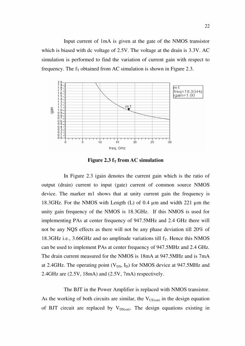
Input current of 1mA is given at the gate of the NMOS transistor
which is biased with dc voltage of 2.5V. The voltage at the drain is 3.3V. AC
simulation is performed to find the variation of current gain with respect to
frequency. The fT obtained from AC simulation is shown in Figure 2.3.
Figure 2.3 fT from AC simulation
In Figure 2.3 igain denotes the current gain which is the ratio of
output (drain) current to input (gate) current of common source NMOS
device. The marker m1 shows that at unity current gain the frequency is
18.3GHz. For the NMOS with Length (L) of 0.4 µm and width 221 µm the
unity gain frequency of the NMOS is 18.3GHz. If this NMOS is used for
implementing PAs at center frequency of 947.5MHz and 2.4 GHz there will
not be any NQS effects as there will not be any phase deviation till 20% of
18.3GHz i.e., 3.66GHz and no amplitude variations till fT. Hence this NMOS
can be used to implement PAs at center frequency of 947.5MHz and 2.4 GHz.
The drain current measured for the NMOS is 18mA at 947.5MHz and is 7mA
at 2.4GHz. The operating point (VDS, ID) for NMOS device at 947.5MHz and
2.4GHz are (2.5V, 18mA) and (2.5V, 7mA) respectively.
The BJT in the Power Amplifier is replaced with NMOS transistor.
As the working of both circuits are similar, the VCE(sat) in the design equation
of BJT circuit are replaced by VDS(sat). The design equations existing in
23
Nathan Sokal et al (1975) are for BJT and the equations are modified for
NMOS and used for finding the circuit components of the Class E PA shown
in Figure 2.1 are as follows
22
DS(sat)DS(sat)
L 2
a
DDD
a
D0.577 V V(V V ) 2R
P P1
4
(2.3)
L LQ RL
2 f (2.4)
1 2L
L
1 1C
2 fR 5.4472 fR 1
4 2
(2.5)
2 1
L L
5.447 1.42C C 1
Q Q 2.08 (2.6)
The design specifications for PA include center frequency
(frequency of operation), bandwidth, Power Added Efficiency (PAE), Noise
Figure (NF), Signal to Noise Ratio (SNR), Spurious Free Dynamic Range
(SFDR) and Power consumption. The design specification of the PAs
operating in different bands of frequencies is given in Table 2.2.
Table 2.2 Design Specification of the PAs
Parameters Power Amplifier1 (PA1) Power Amplifier1 (PA2)
Center frequency 947.5MHz 2.4GHz
Bandwidth 25MHz 20MHz
Power Added Efficiency(PAE) >50% >50%
NF 6dB maximum 6dB maximum
SNR >60 >60
SFDR >40 >40
Power consumption <50nW <50nW
24
Based on the design equations, for the specifications mentioned in
Table 2.2 the values of the components used in the circuit of PA are given in
Table 2.3. The component values given in the Table 2.3 are for the conditions
of maximum power at the load.
Table 2.3 Values of components in Class-E Power Amplifiers
Components PA1 PA2
RL ( ) 1.521 0.12
C1 (pF) 3.4 0.3898
C2 (pF) 21.1915 27.2462
L (nH) 9.4839 9.8534
2.4 SIMULATION OF POWER AMPLIFIERS
The simulation of power amplifiers working in the 900MHz and
2.4GHz range are explained. The various simulations performed are transient
simulation, S-parameter simulation, AC simulation, Load Pull simulation and
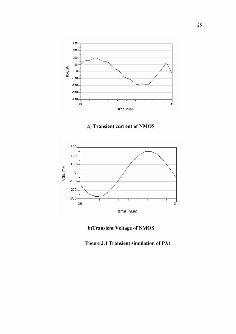
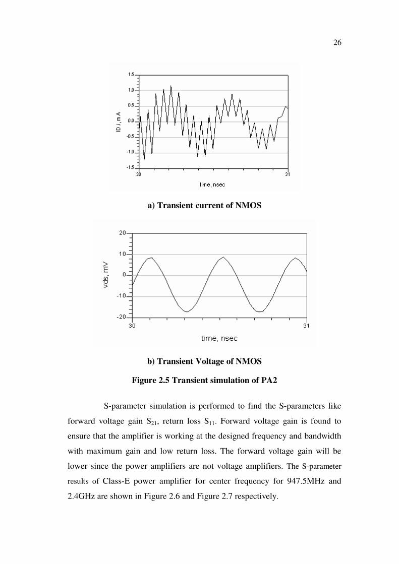
Harmonic Balance simulation. Transient simulation is performed to find
whether the product of voltage and current is low during the RF period. The
results of transient simulation for the PA operating at center frequency of
947.5MHz and 2.4GHz are shown in Figure 2.4 and 2.5 respectively.
From the Figures 2.4 and 2.5, it is inferred that when the voltage is
high, the current is low and when voltage is low current is high. MOSFET
sustains high voltage during one part of the RF period and conduct high
current during the other part of the RF period, the circuit provide output such
that high voltage and high current do not exist at the same time. The product
of MOSFET voltage and current is low at all times during the RF period for
both the PAs PA1 and PA2.
25
a) Transient current of NMOS
b)Transient Voltage of NMOS
Figure 2.4 Transient simulation of PA1
26
a) Transient current of NMOS
b) Transient Voltage of NMOS
Figure 2.5 Transient simulation of PA2
S-parameter simulation is performed to find the S-parameters like
forward voltage gain S21, return loss S11. Forward voltage gain is found to
ensure that the amplifier is working at the designed frequency and bandwidth
with maximum gain and low return loss. The forward voltage gain will be
lower since the power amplifiers are not voltage amplifiers. The S-parameter
results of Class-E power amplifier for center frequency for 947.5MHz and
2.4GHz are shown in Figure 2.6 and Figure 2.7 respectively.
27
a) Forward Voltage Gain (S21)
b) Return Loss (S11)
Figure 2.6 S-parameters of PA1
The S-parameters S21 and S11 are measured in dB as dB(S(2,1)) and
dB(S(1,1)).The S-parameter results in Figure 2.6 show that the PA1 has
maximum gain (S21) given by marker m1 and minimum return loss (S11) given
by marker m4 at 947.5MHz. PA1 provides a bandwidth of 25MHz given by
the difference between the -3dB frequencies specified by markers m2 and m3
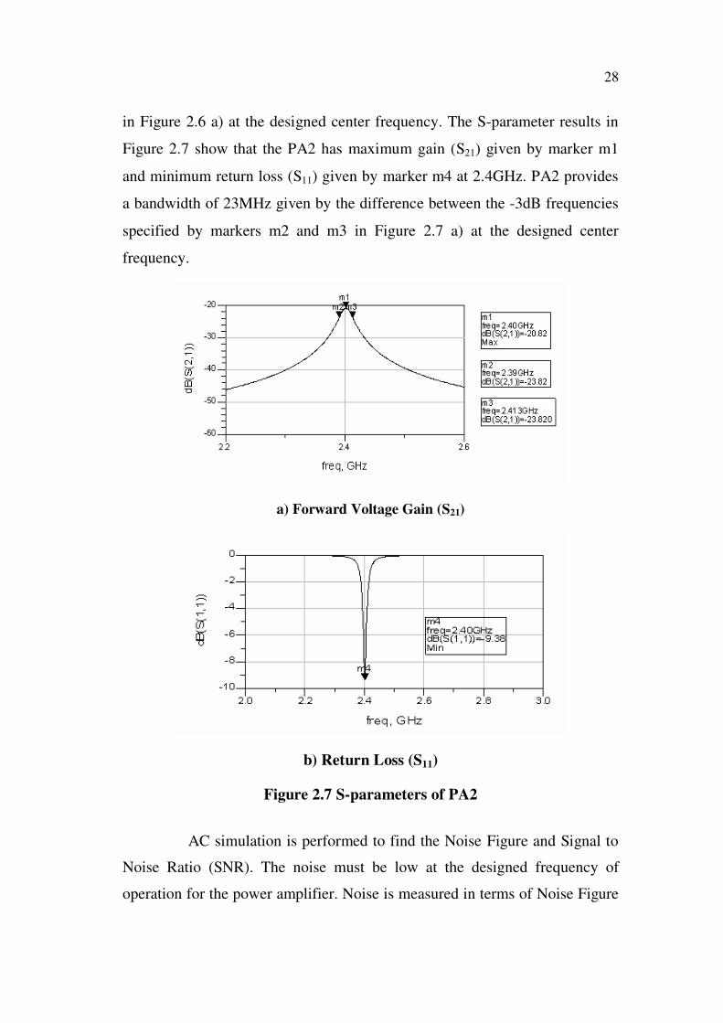
28
in Figure 2.6 a) at the designed center frequency. The S-parameter results in
Figure 2.7 show that the PA2 has maximum gain (S21) given by marker m1
and minimum return loss (S11) given by marker m4 at 2.4GHz. PA2 provides
a bandwidth of 23MHz given by the difference between the -3dB frequencies
specified by markers m2 and m3 in Figure 2.7 a) at the designed center
frequency.
a) Forward Voltage Gain (S21)
b) Return Loss (S11)
Figure 2.7 S-parameters of PA2
AC simulation is performed to find the Noise Figure and Signal to
Noise Ratio (SNR). The noise must be low at the designed frequency of
operation for the power amplifier. Noise is measured in terms of Noise Figure
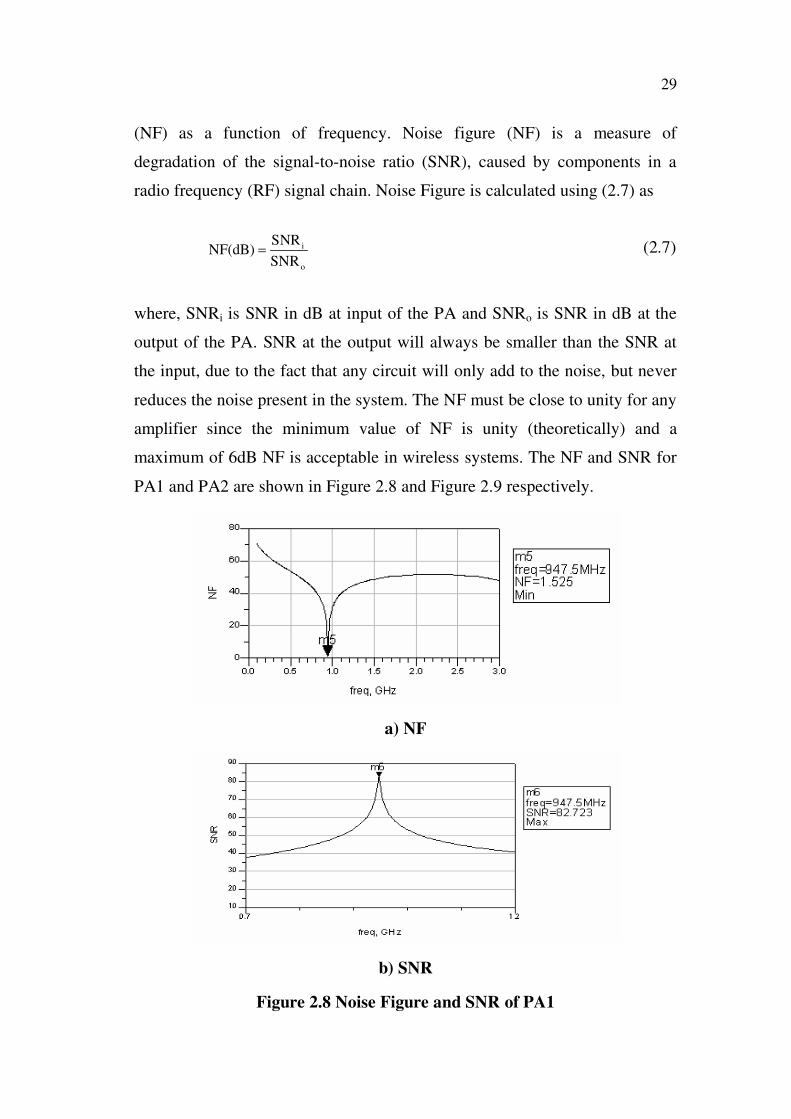
29
(NF) as a function of frequency. Noise figure (NF) is a measure of
degradation of the signal-to-noise ratio (SNR), caused by components in a
radio frequency (RF) signal chain. Noise Figure is calculated using (2.7) as
i
o
SNRNF(dB)
SNR (2.7)
where, SNRi is SNR in dB at input of the PA and SNRo is SNR in dB at the
output of the PA. SNR at the output will always be smaller than the SNR at
the input, due to the fact that any circuit will only add to the noise, but never
reduces the noise present in the system. The NF must be close to unity for any
amplifier since the minimum value of NF is unity (theoretically) and a
maximum of 6dB NF is acceptable in wireless systems. The NF and SNR for
PA1 and PA2 are shown in Figure 2.8 and Figure 2.9 respectively.
a) NF
b) SNR
Figure 2.8 Noise Figure and SNR of PA1
30
a) NF
b)SNR
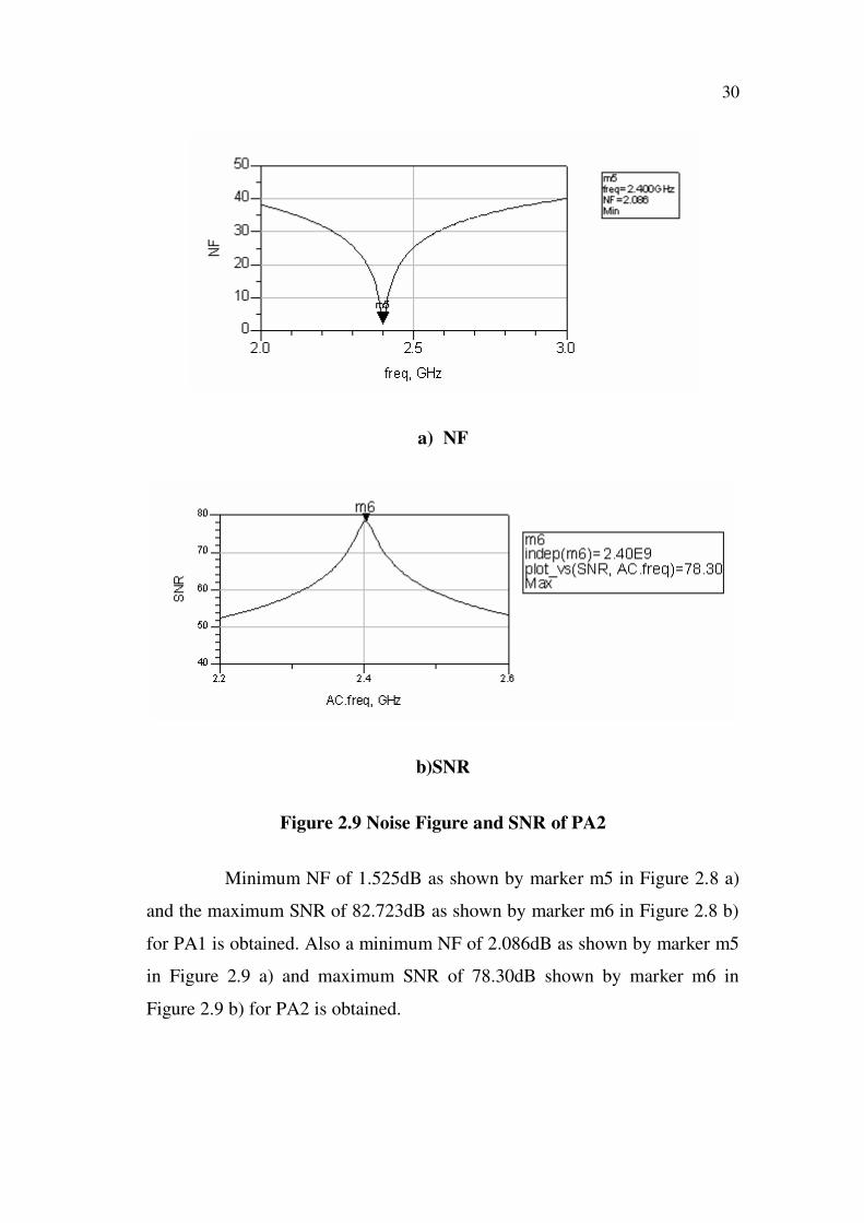
Figure 2.9 Noise Figure and SNR of PA2
Minimum NF of 1.525dB as shown by marker m5 in Figure 2.8 a)
and the maximum SNR of 82.723dB as shown by marker m6 in Figure 2.8 b)
for PA1 is obtained. Also a minimum NF of 2.086dB as shown by marker m5
in Figure 2.9 a) and maximum SNR of 78.30dB shown by marker m6 in
Figure 2.9 b) for PA2 is obtained.
31
Harmonic Balance simulation is performed to find the Power
Added Efficiency (PAE), 1-dB compression values, Spurious Free Dynamic
Range (SFDR) and Third order Intercept Point (IP3), for the power
amplifiers. PAE, impedance and output power delivered by PA are found
using one tone load pull simulation for the fundamental frequency at load
impedance. Power amplifier design requires device characterization for
power, efficiency and reflection coefficients as a function of input power
level. Bias conditions, output circuit loss, load impedance, and gain are the
major design considerations to achieve the required amplifier performance.
Designing the output-match network for power amplifiers is
different from the complex-conjugate matching technique used for small-
signal linear amplifiers. This is because the output impedance of power
devices varies as a function of output power. Ideal termination impedance is
required to maximize the output power available from the amplifier. The
wireless systems are matched at input and output with characteristic
impedance of 50 ohms. The goal of the output-matching network is to
transform 50 ohms into this ideal impedance.
There are two methods to find the ideal output impedance presented
to the MOSFET of the amplifier. One is to perform a load-pull analysis and
the other method is to design a matching network based on the physical model
of the output device, load-line analysis. In load-line analysis the device is
terminated with this load impedance and the source is conjugate matched to
provide maximum gain. In this work Load-pull analysis is performed for the
power amplifiers designed at 947.5MHz and 2.4GHz.
The load-pull data provides the load impedance that corresponds to
different output power levels. For any output power, less than the maximum,
a locus of impedance values form a closed contour on the output impedance
plane. For maximum power, the contour converges to a single point. From the
32
load contours, optimum load impedance to design an output matching
network for maximum power transfer can be found. Load-pull method
provides more accuracy and optimum load impedance.
Load-pull analysis is performed by having various load impedances
at the output of power amplifier and measuring the output power
simultaneously. The input match is adjusted to ensure matched condition at
the input of the amplifier. For each specific impedance value, output power is
measured. The minimum available source power (Pavs) of 23dBm in wireless
systems for which the PA has to deliver maximum power to the load is given
as input for the load-pull simulation and the bias voltages are given as
Vhigh=3.3V and Vlow=2.75V based on the 0.35µm CMOS technology used.
The characteristic impedance Zo is 50 ohms for both the power amplifiers
operating at 947.5MHz and 2.4GHz. The load-pull simulation gives the
Power Added Efficiency (PAE) of an amplifier. The PAE is calculated using
(2.8), as specified in Marian Kazimierczuk (2008).
Output power Drive powerPAE
DC supply power (2.8)
The results for Power Amplifier (PA) designed at 947.5MHz (PA1)
provide a PAE of 71.967% and the power delivered to the load is 29.29dBm.
For power amplifier designed at 2.4GHz (PA2) the PAE of 79.20% is
obtained and the power delivered to the load is 31dBm.
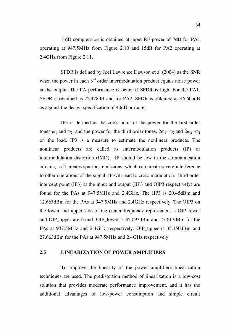
1-dB compression point is found using Harmonic Balance
simulation to find the variation of the output with input as a function of RF
power. 1dB compression point is the point where the circuit gives an output
power of 1dB less than the actual output power required. At the power level
greater than 1dB gain compression point, the amplifier will generate very high
harmonic distortion components. 1dB compression point is determined from
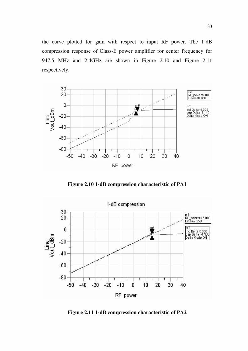
33
the curve plotted for gain with respect to input RF power. The 1-dB
compression response of Class-E power amplifier for center frequency for
947.5 MHz and 2.4GHz are shown in Figure 2.10 and Figure 2.11
respectively.
Figure 2.10 1-dB compression characteristic of PA1
Figure 2.11 1-dB compression characteristic of PA2
34
1-dB compression is obtained at input RF power of 7dB for PA1
operating at 947.5MHz from Figure 2.10 and 15dB for PA2 operating at
2.4GHz from Figure 2.11.
SFDR is defined by Joel Lawrence Dawson et al (2004) as the SNR
when the power in each 3rd
order intermodulation product equals noise power
at the output. The PA performance is better if SFDR is high. For the PA1,
SFDR is obtained as 72.478dB and for PA2, SFDR is obtained as 46.605dB
as against the design specification of 40dB or more.
IP3 is defined as the cross point of the power for the first order
tones 1 and 2, and the power for the third order tones, 2 1- 2 and 2 2- 1
on the load. IP3 is a measure to estimate the nonlinear products. The
nonlinear products are called as intermodulation products (IP) or
intermodulation distortion (IMD). IP should be low in the communication
circuits, as it creates spurious emissions, which can create severe interference
to other operations of the signal. IP will lead to cross modulation. Third order
intercept point (IP3) at the input and output (IIP3 and OIP3 respectively) are
found for the PAs at 947.5MHz and 2.4GHz. The IIP3 is 20.45dBm and
12.663dBm for the PAs at 947.5MHz and 2.4GHz respectively. The OIP3 on
the lower and upper side of the center frequency represented as OIP_lower
and OIP_upper are found. OIP_lower is 35.093dBm and 27.613dBm for the
PAs at 947.5MHz and 2.4GHz respectively. OIP_upper is 35.450dBm and
27.663dBm for the PAs at 947.5MHz and 2.4GHz respectively.
2.5 LINEARIZATION OF POWER AMPLIFIERS
To improve the linearity of the power amplifiers linearization
techniques are used. The predistortion method of linearization is a low-cost
solution that provides moderate performance improvement, and it has the
additional advantages of low-power consumption and simple circuit
35
configuration over other linearization methods proposed by Cebrail Ciftlikli
et al (2007).
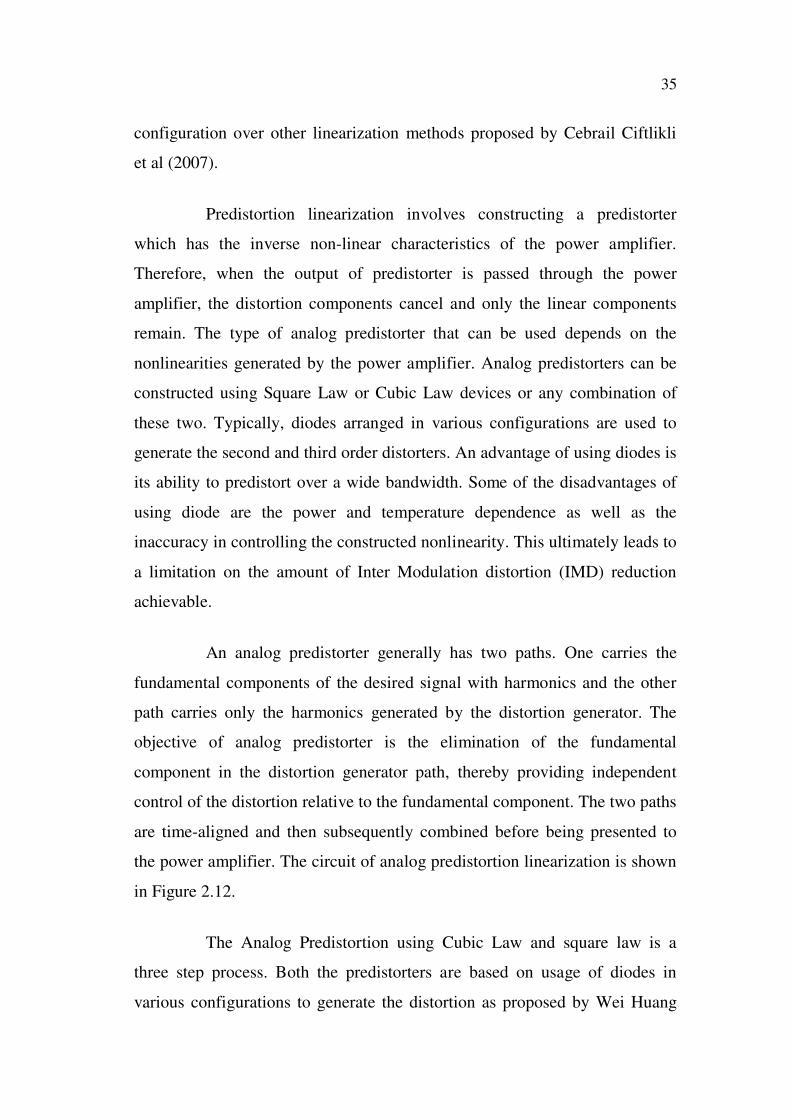
Predistortion linearization involves constructing a predistorter
which has the inverse non-linear characteristics of the power amplifier.
Therefore, when the output of predistorter is passed through the power
amplifier, the distortion components cancel and only the linear components
remain. The type of analog predistorter that can be used depends on the
nonlinearities generated by the power amplifier. Analog predistorters can be
constructed using Square Law or Cubic Law devices or any combination of
these two. Typically, diodes arranged in various configurations are used to
generate the second and third order distorters. An advantage of using diodes is
its ability to predistort over a wide bandwidth. Some of the disadvantages of
using diode are the power and temperature dependence as well as the
inaccuracy in controlling the constructed nonlinearity. This ultimately leads to
a limitation on the amount of Inter Modulation distortion (IMD) reduction
achievable.
An analog predistorter generally has two paths. One carries the
fundamental components of the desired signal with harmonics and the other
path carries only the harmonics generated by the distortion generator. The
objective of analog predistorter is the elimination of the fundamental
component in the distortion generator path, thereby providing independent
control of the distortion relative to the fundamental component. The two paths
are time-aligned and then subsequently combined before being presented to
the power amplifier. The circuit of analog predistortion linearization is shown
in Figure 2.12.
The Analog Predistortion using Cubic Law and square law is a
three step process. Both the predistorters are based on usage of diodes in
various configurations to generate the distortion as proposed by Wei Huang
36
and Ricardo Saad (1998). The diodes can be biased to better approximate the
type of nonlinear behavior that is required. The predistorter consist of two
paths; one to generate the nonlinearity and the other to pass the fundamental
components.
Power splitter
Square/
cubic law
predistorer
Complex
gain
adjuster
Power combiner
output
signal
input signal Time delay
unit
Vdc=alpha_Q
Power
amplifier
Vdc=alpha_I
Figure 2.12 Circuit of Analog Predistortion Linearization
A hybrid is used in the distortion generation path for eliminating
the fundamental component. A complex gain adjuster is then used to control
the amplitude and phase of the distortion relative to the fundamental
component. The complex gain adjuster acts as a vector modulator. The input
signal is split into two branches in the complex gain adjuster, each branch
being individually controlled by in-phase (I) and quadrature (Q) inputs. The
output is the sum of the two branches. The two branches of the vector
modulator are in phase quadrature and the mixer elements are implemented
using ideal multipliers. The voltage applied to the complex gain adjuster
through alpha_I and alpha_Q is varied between -2V to +2V for varying the
magnitude.
37
The steps in square law method of analog predistortion for
linearization of PA are
Finding the Square law predistorter dependence on power and
bias voltage
Optimization of square law predistorter and
Square law predistortion of the PA
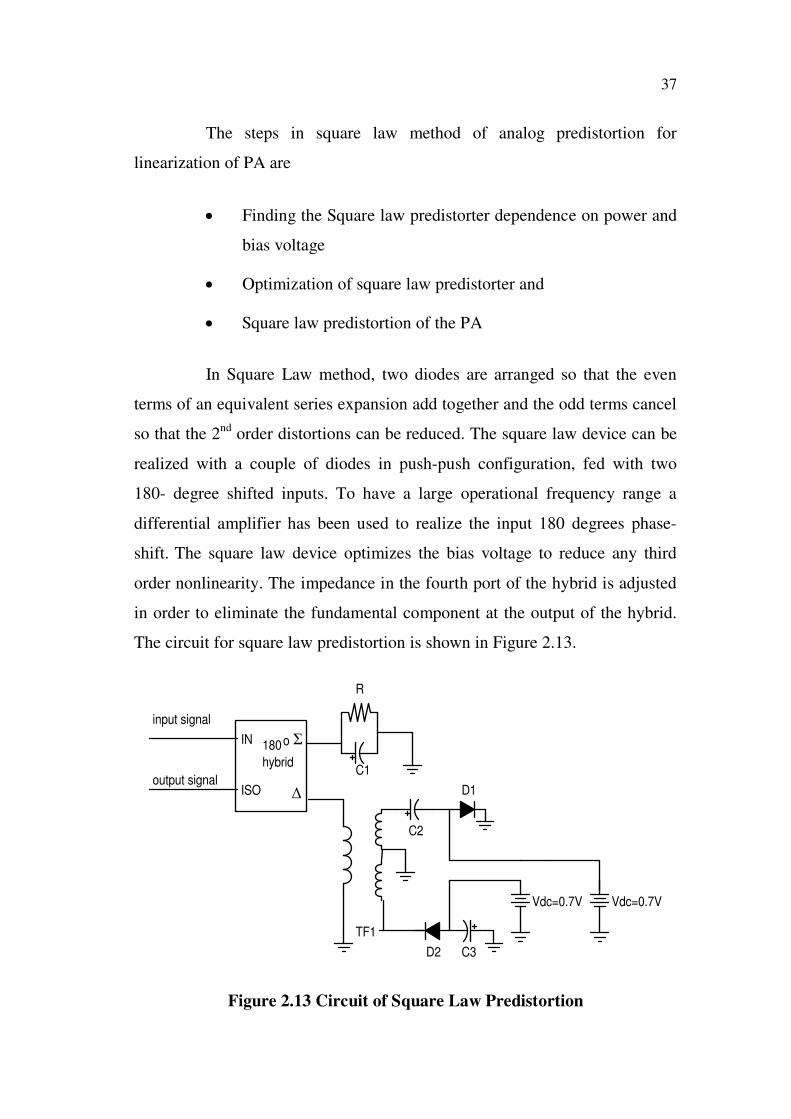
In Square Law method, two diodes are arranged so that the even
terms of an equivalent series expansion add together and the odd terms cancel
so that the 2nd
order distortions can be reduced. The square law device can be
realized with a couple of diodes in push-push configuration, fed with two
180- degree shifted inputs. To have a large operational frequency range a
differential amplifier has been used to realize the input 180 degrees phase-
shift. The square law device optimizes the bias voltage to reduce any third
order nonlinearity. The impedance in the fourth port of the hybrid is adjusted
in order to eliminate the fundamental component at the output of the hybrid.
The circuit for square law predistortion is shown in Figure 2.13.
Figure 2.13 Circuit of Square Law Predistortion
180o
hybrid
input signal
output signalC1
R
D1
D2 C3
TF1
Vdc=0.7VVdc=0.7V
C2
ISO
IN
38
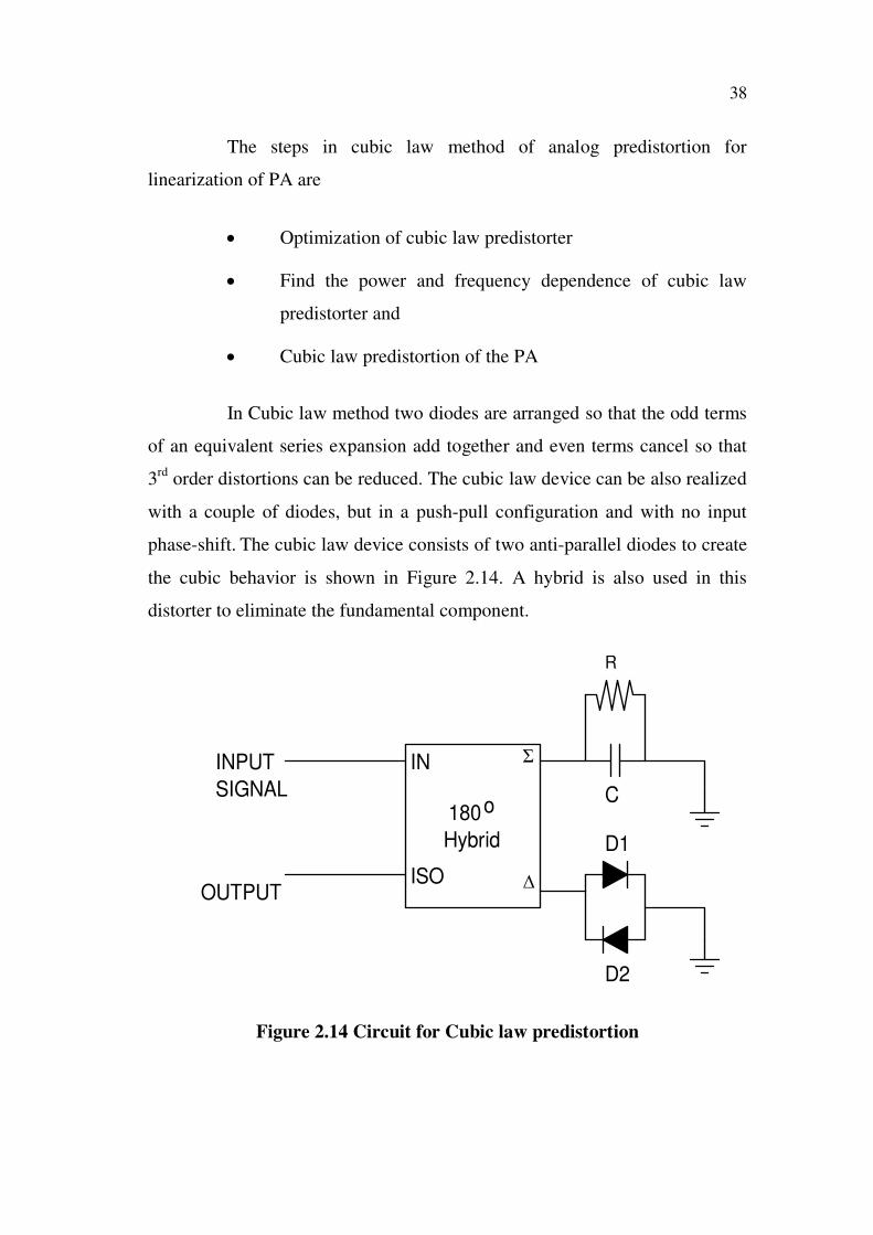
The steps in cubic law method of analog predistortion for
linearization of PA are
Optimization of cubic law predistorter
Find the power and frequency dependence of cubic law
predistorter and
Cubic law predistortion of the PA
In Cubic law method two diodes are arranged so that the odd terms
of an equivalent series expansion add together and even terms cancel so that
3rd
order distortions can be reduced. The cubic law device can be also realized
with a couple of diodes, but in a push-pull configuration and with no input
phase-shift. The cubic law device consists of two anti-parallel diodes to create
the cubic behavior is shown in Figure 2.14. A hybrid is also used in this
distorter to eliminate the fundamental component.
Figure 2.14 Circuit for Cubic law predistortion
180o
Hybrid
INPUT
SIGNAL
OUTPUT
R
D1
C
D2
IN
ISO
39
2.6 SIMULATION RESULTS OF LINEARIZATION
Linearization is performed for the PAs working at center frequency
of 947.5MHz and 2.4GHz using square Law and cubic law methods. In
square law method the first step is to find the power in the harmonics at the
output of the predistorter circuit and dependence on power and bias voltage.
In the predistorter circuit 180° Hybrid coupler is used to phase shift the signal
by 180°. The hybrid coupler has reference impedance of 50 ohms and loss of
0dB. The dependence of power is measured in terms of carrier to Inter
Modulation Distortion (IMD) ratio in dBc. For the voltage of 0.7V in forward
bias for the diodes and available source power the C/IMD ratio is 1.047dBc
for PA1 and 1.026dBc for PA2. In the second step of square law predistortion,
gradient optimization is performed to suppress the fundamental frequency
components and the 2nd
order intermodulation power in the upper and lower
sidebands at the designed center frequency. The value of resistor and
capacitor are R=2315ohms c=1µF.
In the third step the power amplifier is connected with the
predistorter as shown in Figure 2.12. The linearization using square law
method of analog predistortion suppresses the harmonics and thereby the
linearity of the amplifier is improved. The C/IMD ratio is improved to
71.37dBc for PA1 and 69.77dBc for PA2 after linearization. The power in the
harmonics at output of each stage in the square law predistortion linearization
for the PA1 and PA2 are given in Table 2.4.
40
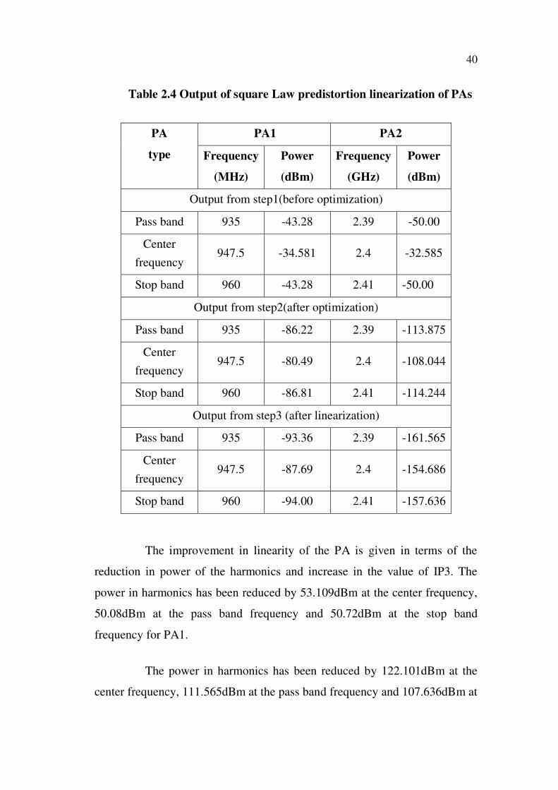
Table 2.4 Output of square Law predistortion linearization of PAs
PA1 PA2PA
type Frequency
(MHz)
Power
(dBm)
Frequency
(GHz)
Power
(dBm)
Output from step1(before optimization)
Pass band 935 -43.28 2.39 -50.00
Center
frequency947.5 -34.581 2.4 -32.585
Stop band 960 -43.28 2.41 -50.00
Output from step2(after optimization)
Pass band 935 -86.22 2.39 -113.875
Center
frequency947.5 -80.49 2.4 -108.044
Stop band 960 -86.81 2.41 -114.244
Output from step3 (after linearization)
Pass band 935 -93.36 2.39 -161.565
Center
frequency947.5 -87.69 2.4 -154.686
Stop band 960 -94.00 2.41 -157.636
The improvement in linearity of the PA is given in terms of the
reduction in power of the harmonics and increase in the value of IP3. The
power in harmonics has been reduced by 53.109dBm at the center frequency,
50.08dBm at the pass band frequency and 50.72dBm at the stop band
frequency for PA1.
The power in harmonics has been reduced by 122.101dBm at the
center frequency, 111.565dBm at the pass band frequency and 107.636dBm at
41
the stop band frequency for PA2. The improvement in IP3 and power
consumption after linearization using square law analog predistortion is given
in Table 2.5.
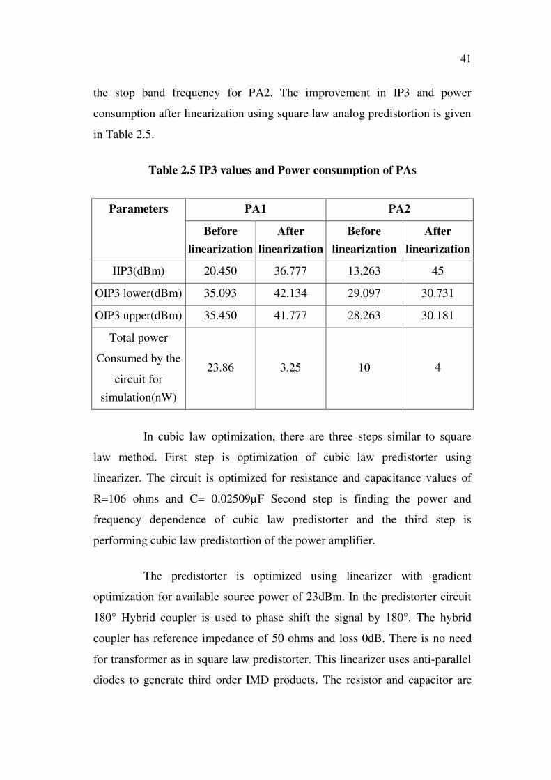
Table 2.5 IP3 values and Power consumption of PAs
PA1 PA2Parameters
Before
linearization
After
linearization
Before
linearization
After
linearization
IIP3(dBm) 20.450 36.777 13.263 45
OIP3 lower(dBm) 35.093 42.134 29.097 30.731
OIP3 upper(dBm) 35.450 41.777 28.263 30.181
Total power
Consumed by the
circuit for
simulation(nW)
23.86 3.25 10 4
In cubic law optimization, there are three steps similar to square
law method. First step is optimization of cubic law predistorter using
linearizer. The circuit is optimized for resistance and capacitance values of
R=106 ohms and C= 0.02509µF Second step is finding the power and
frequency dependence of cubic law predistorter and the third step is
performing cubic law predistortion of the power amplifier.
The predistorter is optimized using linearizer with gradient
optimization for available source power of 23dBm. In the predistorter circuit
180° Hybrid coupler is used to phase shift the signal by 180°. The hybrid
coupler has reference impedance of 50 ohms and loss 0dB. There is no need
for transformer as in square law predistorter. This linearizer uses anti-parallel
diodes to generate third order IMD products. The resistor and capacitor are
42
used to reduce the fundamental output component relative to the third order
IMD products. The fundamental component is suppressed at the output of the
predistorter and the carrier to Inter Modulation Distortion (IMD) ratio C/IMD
in dBc reduces with number of iterations of the optimization. C/IMD is
measured as the power with respect to carrier power of the input signal in
dBc.
In the second step of predistortion, the variation of the signal
C/IMD with respect to power and frequency are observed and the spectrum is
180° phase shifted. The C/IMD ratio variation observed with respect to
frequency and power is very closer with the expected variation of C/IMD
ratio and the output spectrum from the predistorter is maximum at the desired
center frequencies for both the power amplifiers. For the voltage of 0.7V in
forward bias for the diodes and available source power the C/IMD ratio is
24.156dBc for PA1 and 19.918dBc for PA2.
The third step in analog predistortion using cubic law the
predistorter is connected with the power amplifier along with complex gain
adjuster circuit. The complex gain adjuster circuit behaves like a vector
modulator and controls the amplitude and phase of the signal. The signal is
split into inphase and quadrature components by 90° hybrid and the
components are multiplied by the control voltage and finally combined by
power combiner. The power combiner has an isolation of 100dB between the
port 2 and port 3 of the combiner. The impedance at all the ports is 50 ohms.
The combiner is selected such that the S-parameters are as follows:S21=1,
S31=1, S11=0 and S22=0.
The optimum value of the coefficients for optimization are given in
Table 2.6 and Table 2.7 for PA with 947.5MHz and 2.4GHz respectively.
43
Table 2.6 Optimization coefficients and optimum time delay for
947.5MHz
No. of
Iterations
Inphase
coefficients
Quadrature
coeficients
Time delay
(nsec)
0 0 0 0.1
1 1.948 1.933 1.125
2 1.948 1.933 1.125
3 1.927 1.953 1.126
4 1.914 1.962 1.126
5 1.908 1.958 1.126
6 1.902 1.954 1.126
7 1.902 1.954 1.124
8 1.879 1.950 1.125
9 1.872 1.946 1.125
10 1.872 1.946 1.124
11 1.704 1.922 1.124
12 1.703 1.916 1.124
Table 2.7 Optimization coefficients and optimum time delay for 2.4GHz
No. of
Iterations
Inphase
coefficients
Quadrature
coeficients
Time delay
(nsec)
0 0 0 0.1
1 0.258 1.017 7.985
2 -1.072 -1.456 6.506
3 -1.071 -1.455 6.505
4 -1.061 -1.465 6.505
5 -1.052 -1.475 6.505
6 -1.043 -1.485 6.505
7 -1.034 -1.495 6.505
8 -1.025 -1.505 6.505
9 -1.016 -1.515 6.504
10 -1.00 -1.525 6.504
11 -0.998 -1.535 6.504
12 -0.989 -1.545 6.504
44
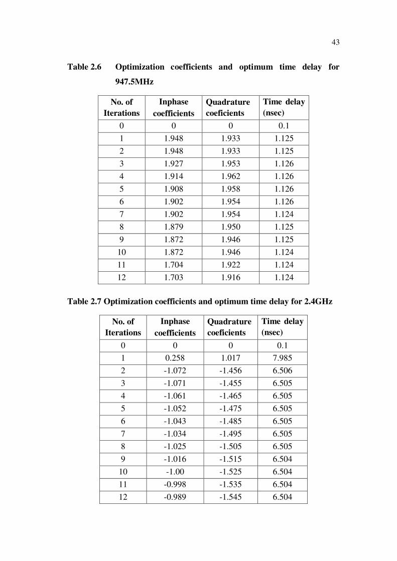
The simulation results of cubic law perdistortion linearization of PAs is given
in Table 2.8.
Table 2.8 IP3 values and Power consumption of PAs
PA1 PA2Parameters
Before
linearization
After
linearization
Before
linearization
After
linearization
IIP3(dBm) 20.450 47 13.263 70
OIP3
lower(dBm)35.093 38.799 29.097 56
OIP3
upper(dBm)32.936 32.936 28.263 55
Total power
Consumed by the
circuit
23.86nW 1.637nW 10nW 6nW
The power in the harmonics at output of each stage in the square law
predistortion linearization for the PA1 and PA2 are given in Table 2.9
Table 2.9 Output of Cubic Law predistortion linearization of PAs
PA1 PA2PA
type Frequency
(MHz)
Power
(dBm)
Frequency
(GHz)
Power
(dBm)
Output from step1(before optimization)
Pass band 935 -18.064 2.39 -54.91
Center
frequency947.5 -29.583 2.4 -15.185
Stop band 960 -29.689 2.41 -28.226
Output from step2(after optimization)
Pass band 935 -39.434 2.39 -80.578
Center
frequency947.5 -40.265 2.4 -82.859
Stop band 960 -41.092 2.41 -80.469
Output from step3 (after linearization)
Pass band 935 -42.645 2.39 -82.512
Center
frequency947.5 -43.596 2.4 -92.465
Stop band 960 -44.514 2.41 -83.177
45
The simulation results of the cubic law predistrotion step 3 shows that the
harmonicsl has been decreased when compared to the signal before
predistortion. Also the third order C/IMD ratio in dBc (in dB with respect to
carrier) has increased to 26.823dBc for PA1 and 26.644dBc for PA2 after
linearization. The power in harmonics has been reduced by 14.013dBm at the
center frequency, 24.581dBm at the pass band frequency and 15.125dBm at
the stop band frequency for PA1. The power in harmonics has been reduced
by 77.28dBm at the center frequency, 27.602dBm at the pass band frequency
and 54.951dBm at the stop band frequency for PA2. Hence the linearity of the
power amplifier is improved with analog predistortion methods.
2.7 CONCLUSION
Class-E power amplifiers for two different frequencies of
947.5MHz and 2.4GHz are designed and their performance is studied. The
Class-E amplifiers designed give a PAE of 71.967% at 947.5MHz and
79.20% at 2.4GHz. Both the amplifiers give a PAE of above 70% when
compared to the power amplifiers in the literature with PAE 64%. The noise
figure of 1.575 for 947.5MHz and 2.086 for 2.4GHz is obtained which is less
than desirable value of Noise Figure of 6 for power amplifiers in wireless
systems. The SNR is 82.723 and SFDR is 72.478dB for PA at 947.5MHz.
The SNR is 78.34dB and SFDR is 46.605dB for PA operating at 2.4GHz.
Both the PAs provide a very good SNR and SFDR. The linearity of the power
amplifiers designed for 947.5MHz and 2.4GHz are improved by square law
and cubic law analog predistortion methods by suppressing the power in
harmonics and increasing the IP3 and C/IMD ratio. In the square law method
the second order harmonics are suppressed and thereby the linearity of the
amplifiers is improved. In the cubic law predistortion the third order and fifth
order harmonics are reduced to increase the signal strength at the desired
frequencies and the linearity is improved. Linearization of PA1 using square
law and cubic law predistortion saves 20.61nW and 22.22nW of power
respectively. Similarly for PA2, 6nW and 4nW of power are saved by
linearization using square law and cubic law predistortion.