Embed Size (px)
Citation preview

Chapter 15: Design Examples
Digital System Designs and Practices Using Verilog HDL and FPGAs @ 2008-2010, John Wiley 15-1
Chapter 15: Design Examples
Department of Electronic Engineering
National Taiwan University of Science and Technology
Prof. Ming-Bo Lin

Chapter 15: Design Examples
Digital System Designs and Practices Using Verilog HDL and FPGAs @ 2008-2010, John Wiley 15-2
Syllabus
ObjectivesBusData transferGeneral-purpose input and outputTimersUniversal asynchronous receiver and transmitterA simple CPU design
Chapter 15: Design Examples
Digital System Designs and Practices Using Verilog HDL and FPGAs @ 2008-2010, John Wiley 15-3
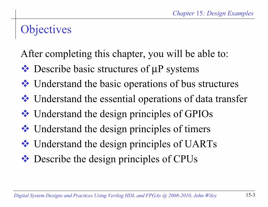
Objectives
After completing this chapter, you will be able to:Describe basic structures of µP systemsUnderstand the basic operations of bus structuresUnderstand the essential operations of data transferUnderstand the design principles of GPIOsUnderstand the design principles of timersUnderstand the design principles of UARTsDescribe the design principles of CPUs

Chapter 15: Design Examples
Digital System Designs and Practices Using Verilog HDL and FPGAs @ 2008-2010, John Wiley 15-4
Syllabus
ObjectivesBus
A µp system architectureBus structuresBus arbitration
Data transferGeneral-purpose input and outputTimersUniversal asynchronous receiver and transmitterA simple CPU design
Chapter 15: Design Examples
Digital System Designs and Practices Using Verilog HDL and FPGAs @ 2008-2010, John Wiley 15-5
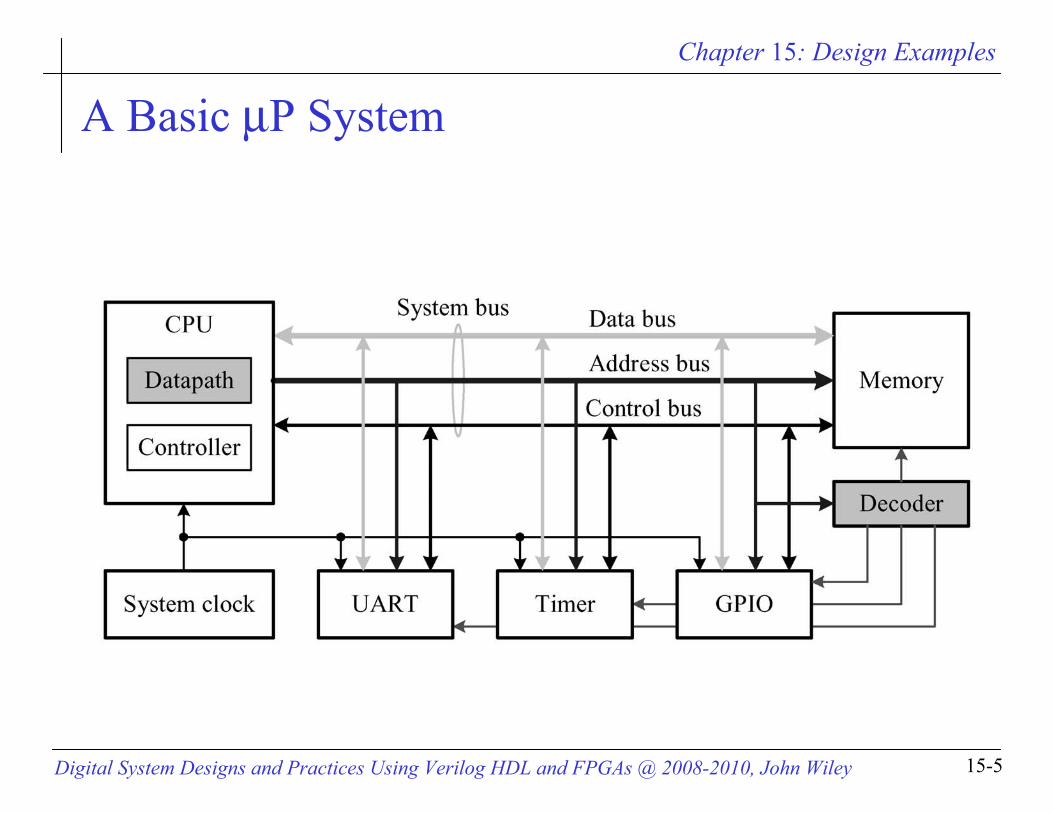
A Basic µP System

Chapter 15: Design Examples
Digital System Designs and Practices Using Verilog HDL and FPGAs @ 2008-2010, John Wiley 15-6
Syllabus
ObjectivesBus
A µp system architectureBus structuresBus arbitration
Data transferGeneral-purpose input and outputTimersUniversal asynchronous receiver and transmitterA simple CPU design

Chapter 15: Design Examples
Digital System Designs and Practices Using Verilog HDL and FPGAs @ 2008-2010, John Wiley 15-7
Bus Structures
Tristate bususing tristate buffersoften called bus for short
Multiplexer-based bususing multiplexers

Chapter 15: Design Examples
Digital System Designs and Practices Using Verilog HDL and FPGAs @ 2008-2010, John Wiley 15-8
A Tristate Bus

Chapter 15: Design Examples
Digital System Designs and Practices Using Verilog HDL and FPGAs @ 2008-2010, John Wiley 15-9
A Tristate Bus Example
// a tristate bus examplemodule tristate_bus (data, enable, qout);parameter N = 2; // define bus widthinput enable;input [N-1:0] data;output [N-1:0] qout;wire [N-1:0] qout;
// the body of tristate busassign qout = enable ? data : {N{1'bz}};endmodule
Chapter 15: Design Examples
Digital System Designs and Practices Using Verilog HDL and FPGAs @ 2008-2010, John Wiley 15-10
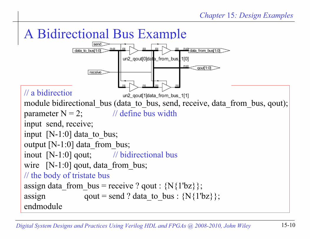
A Bidirectional Bus Example
// a bidirectional bus examplemodule bidirectional_bus (data_to_bus, send, receive, data_from_bus, qout);parameter N = 2; // define bus widthinput send, receive;input [N-1:0] data_to_bus;output [N-1:0] data_from_bus;inout [N-1:0] qout; // bidirectional buswire [N-1:0] qout, data_from_bus;// the body of tristate busassign data_from_bus = receive ? qout : {N{1'bz}};assign qout = send ? data_to_bus : {N{1'bz}};endmodule

Chapter 15: Design Examples
Digital System Designs and Practices Using Verilog HDL and FPGAs @ 2008-2010, John Wiley 15-11
A Multiplexer-Based Bus

Chapter 15: Design Examples
Digital System Designs and Practices Using Verilog HDL and FPGAs @ 2008-2010, John Wiley 15-12
Syllabus
ObjectivesBus
A µp system architectureBus structuresBus arbitration
Data transferGeneral-purpose input and outputTimersUniversal asynchronous receiver and transmitterA simple CPU design

Chapter 15: Design Examples
Digital System Designs and Practices Using Verilog HDL and FPGAs @ 2008-2010, John Wiley 15-13
Daisy-Chain Arbitration
Types of bus arbitration schemesdaisy-chain arbitrationradial arbitration
Chapter 15: Design Examples
Digital System Designs and Practices Using Verilog HDL and FPGAs @ 2008-2010, John Wiley 15-14
Syllabus
ObjectivesBusData transfer
Synchronous transfer modeAsynchronous transfer mode
General-purpose input and outputTimersUniversal asynchronous receiver and transmitterA simple CPU design
Chapter 15: Design Examples
Digital System Designs and Practices Using Verilog HDL and FPGAs @ 2008-2010, John Wiley 15-15
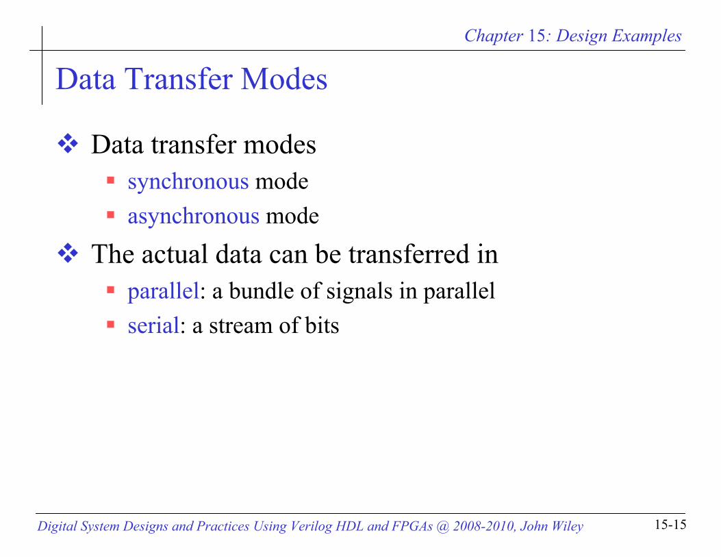
Data Transfer Modes
Data transfer modessynchronous mode asynchronous mode
The actual data can be transferred inparallel: a bundle of signals in parallelserial: a stream of bits

Chapter 15: Design Examples
Digital System Designs and Practices Using Verilog HDL and FPGAs @ 2008-2010, John Wiley 15-16
Synchronously Parallel Data Transfers
Each data transfer is synchronous with clock signalBus masterBus slave
Two typesSingle-clock bus cycleMultiple-clock bus cycle

Chapter 15: Design Examples
Digital System Designs and Practices Using Verilog HDL and FPGAs @ 2008-2010, John Wiley 15-17
Synchronously Parallel Data Transfers
Chapter 15: Design Examples
Digital System Designs and Practices Using Verilog HDL and FPGAs @ 2008-2010, John Wiley 15-18
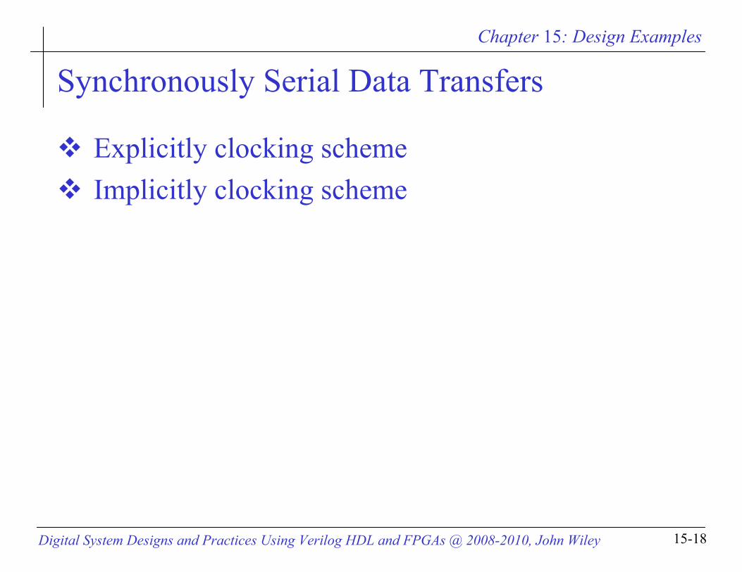
Synchronously Serial Data Transfers
Explicitly clocking schemeImplicitly clocking scheme

Chapter 15: Design Examples
Digital System Designs and Practices Using Verilog HDL and FPGAs @ 2008-2010, John Wiley 15-19
Synchronously Serial Data Transfers
Examples

Chapter 15: Design Examples
Digital System Designs and Practices Using Verilog HDL and FPGAs @ 2008-2010, John Wiley 15-20
Syllabus
ObjectivesBusData transfer
Synchronous transfer modeAsynchronous transfer mode
General-purpose input and outputTimersUniversal asynchronous receiver and transmitterA simple CPU design

Chapter 15: Design Examples
Digital System Designs and Practices Using Verilog HDL and FPGAs @ 2008-2010, John Wiley 15-21
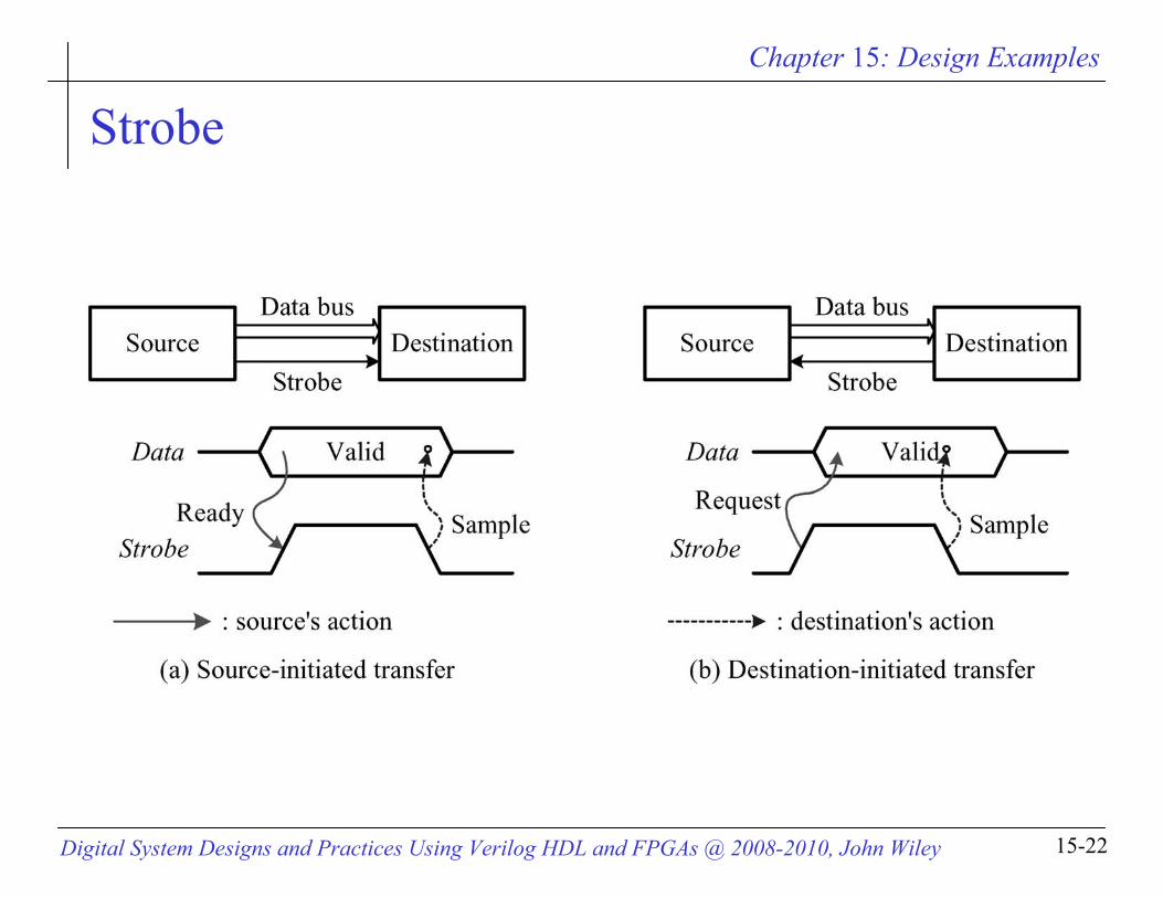
Asynchronous Data Transfers
Each data transfer occurs at randomControl approaches
strobe schemehandshaking scheme
Chapter 15: Design Examples
Digital System Designs and Practices Using Verilog HDL and FPGAs @ 2008-2010, John Wiley 15-22
Strobe

Chapter 15: Design Examples
Digital System Designs and Practices Using Verilog HDL and FPGAs @ 2008-2010, John Wiley 15-23
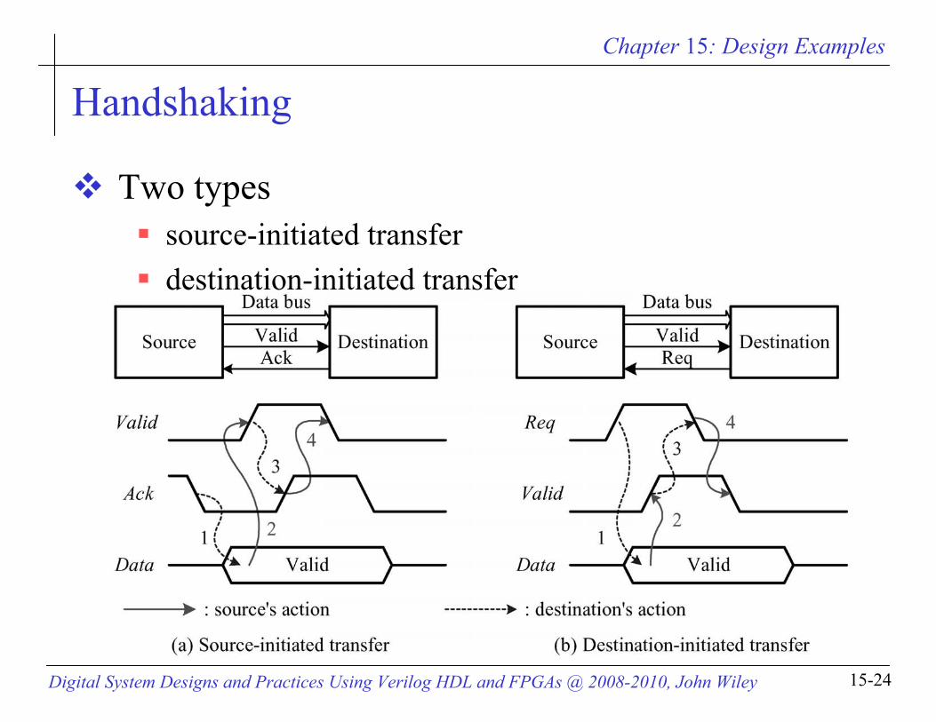
Handshaking
Four events are proceeded in a cycle orderready (request)data valid data acceptanceacknowledge
Chapter 15: Design Examples
Digital System Designs and Practices Using Verilog HDL and FPGAs @ 2008-2010, John Wiley 15-24
Handshaking
Two typessource-initiated transferdestination-initiated transfer
Chapter 15: Design Examples
Digital System Designs and Practices Using Verilog HDL and FPGAs @ 2008-2010, John Wiley 15-25
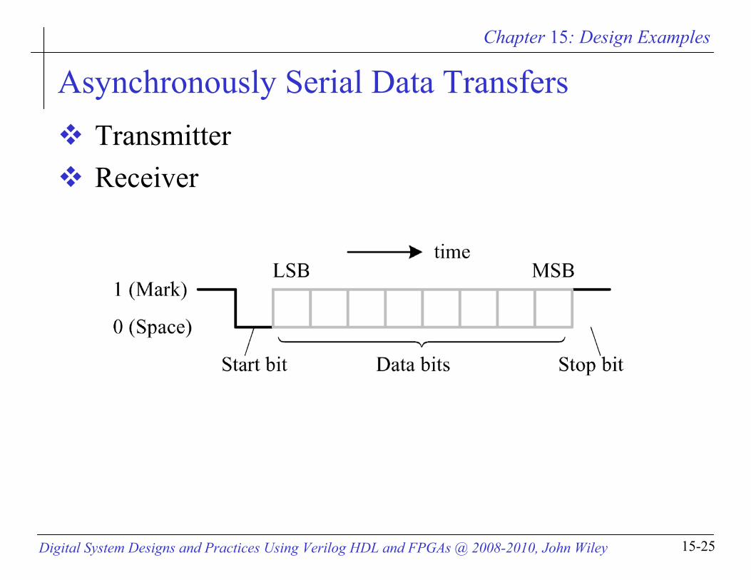
Asynchronously Serial Data TransfersTransmitterReceiver

Chapter 15: Design Examples
Digital System Designs and Practices Using Verilog HDL and FPGAs @ 2008-2010, John Wiley 15-26
Asynchronously Serial Data Transfers
Chapter 15: Design Examples
Digital System Designs and Practices Using Verilog HDL and FPGAs @ 2008-2010, John Wiley 15-27
Syllabus
ObjectivesBusData transferGeneral-purpose input and outputTimersUniversal asynchronous receiver and transmitterA simple CPU design
Chapter 15: Design Examples
Digital System Designs and Practices Using Verilog HDL and FPGAs @ 2008-2010, John Wiley 15-28
General-Purpose Input and Output Devices
The general-purpose input and output (GPIO) inputoutputbidirectional

Chapter 15: Design Examples
Digital System Designs and Practices Using Verilog HDL and FPGAs @ 2008-2010, John Wiley 15-29
General-Purpose Input and Output Devices
An example of 8-bit GPIO

Chapter 15: Design Examples
Digital System Designs and Practices Using Verilog HDL and FPGAs @ 2008-2010, John Wiley 15-30
Design Issues of GPIO Devices
Readback capability of PORT registerGroup or individual bit controlSelection the value of DDRHandshaking controlReadback capability of DDRInput latchInput/Output pull-upDrive capability

Chapter 15: Design Examples
Digital System Designs and Practices Using Verilog HDL and FPGAs @ 2008-2010, John Wiley 15-31
General-Purpose Input and Output Devices
The ith-bit of two GPIO examples
Chapter 15: Design Examples
Digital System Designs and Practices Using Verilog HDL and FPGAs @ 2008-2010, John Wiley 15-32
Syllabus
ObjectivesBusData transferGeneral-purpose input and outputTimers
InterfaceBasic operation modesAdvanced operation modes
Universal asynchronous receiver and transmitterA simple CPU design
Chapter 15: Design Examples
Digital System Designs and Practices Using Verilog HDL and FPGAs @ 2008-2010, John Wiley 15-33
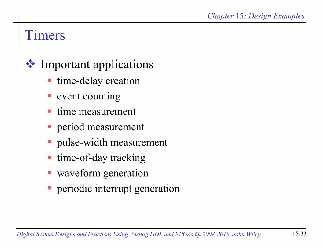
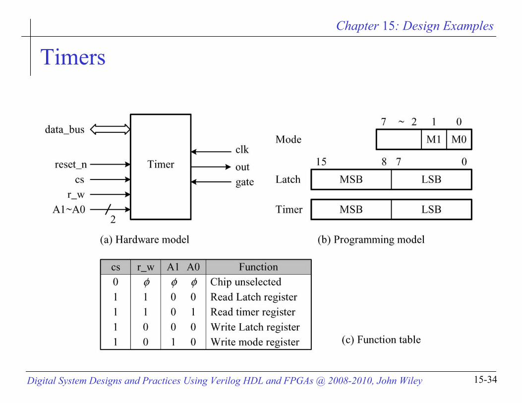
Timers
Important applications time-delay creation event counting time measurement period measurement pulse-width measurement time-of-day trackingwaveform generationperiodic interrupt generation
Chapter 15: Design Examples
Digital System Designs and Practices Using Verilog HDL and FPGAs @ 2008-2010, John Wiley 15-34
Timers

Chapter 15: Design Examples
Digital System Designs and Practices Using Verilog HDL and FPGAs @ 2008-2010, John Wiley 15-35
Syllabus
ObjectivesBusData transferGeneral-purpose input and outputTimers
InterfaceBasic operation modes
Universal asynchronous receiver and transmitterA simple CPU design

Chapter 15: Design Examples
Digital System Designs and Practices Using Verilog HDL and FPGAs @ 2008-2010, John Wiley 15-36
Basic Timer Operations
TimersWhat is a timer?What is a counter?What is a programmable counter?What is a programmable timer?
Basic operation modesterminal count (binary/BCD event counter)rate generation(digital) monostable (or called one-shot)square-wave generation

Chapter 15: Design Examples
Digital System Designs and Practices Using Verilog HDL and FPGAs @ 2008-2010, John Wiley 15-37
Terminal Count

Chapter 15: Design Examples
Digital System Designs and Practices Using Verilog HDL and FPGAs @ 2008-2010, John Wiley 15-38
Rate Generation

Chapter 15: Design Examples
Digital System Designs and Practices Using Verilog HDL and FPGAs @ 2008-2010, John Wiley 15-39
Retriggerable Monostable (One-Shot) Operation

Chapter 15: Design Examples
Digital System Designs and Practices Using Verilog HDL and FPGAs @ 2008-2010, John Wiley 15-40
Square-Wave Generation
(b) Block diagram of square-wave mode
(a) A waveform example of square-wave mode
clk
out
3 2 1 0(4)0(4)3 2 14
Latch register = 4
Latch
timer
Data buswr
rd
out
gateclk
timer_loadgenerator
timer_enable
timer_load DCK
Q
timer is 1
Shift plus LSB
out logic
latch_load

Chapter 15: Design Examples
Digital System Designs and Practices Using Verilog HDL and FPGAs @ 2008-2010, John Wiley 15-41
Syllabus
ObjectivesBusData transferGeneral-purpose input and outputTimersUniversal asynchronous receiver and transmitter
InterfaceBasic transmitter structureBasic receiver structureBaud-rate generators
A simple CPU design
Chapter 15: Design Examples
Digital System Designs and Practices Using Verilog HDL and FPGAs @ 2008-2010, John Wiley 15-42
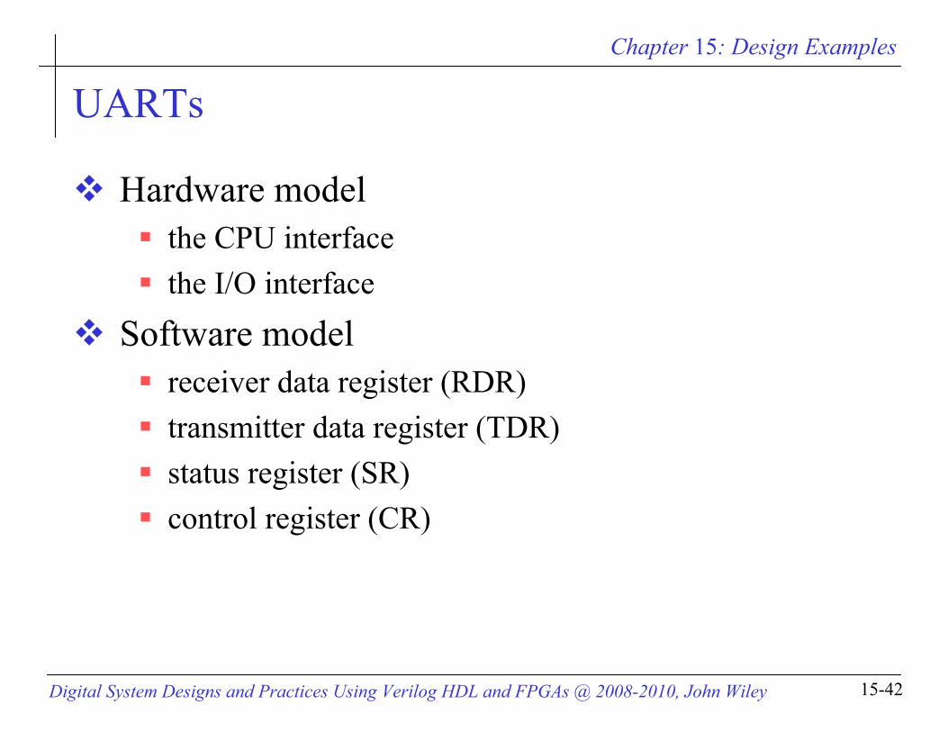
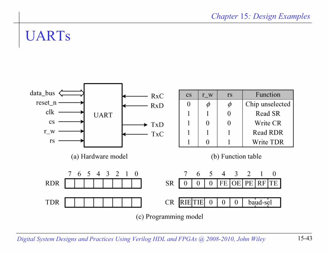
UARTs
Hardware modelthe CPU interfacethe I/O interface
Software model receiver data register (RDR)transmitter data register (TDR) status register (SR)control register (CR)
Chapter 15: Design Examples
Digital System Designs and Practices Using Verilog HDL and FPGAs @ 2008-2010, John Wiley 15-43
UARTs

Chapter 15: Design Examples
Digital System Designs and Practices Using Verilog HDL and FPGAs @ 2008-2010, John Wiley 15-44
Syllabus
ObjectivesBusData transferGeneral-purpose input and outputTimersUniversal asynchronous receiver and transmitter
InterfaceBasic transmitter structureBasic receiver structureBaud-rate generators
A simple CPU design
Chapter 15: Design Examples
Digital System Designs and Practices Using Verilog HDL and FPGAs @ 2008-2010, John Wiley 15-45
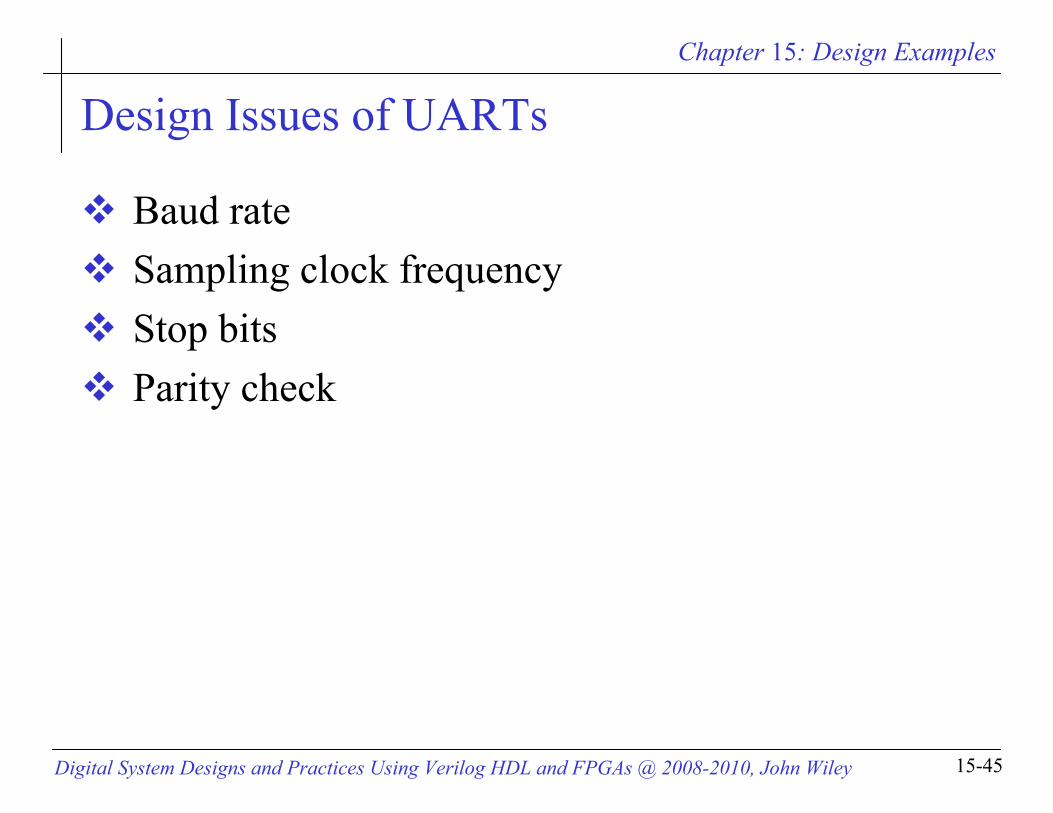
Design Issues of UARTs
Baud rateSampling clock frequencyStop bitsParity check

Chapter 15: Design Examples
Digital System Designs and Practices Using Verilog HDL and FPGAs @ 2008-2010, John Wiley 15-46
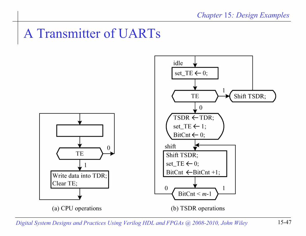
A Transmitter of UARTs
The transmitter a transmitter shift data register (TSDR) a TDR empty flag (TE) a transmitter control circuita TDRparity generator
Chapter 15: Design Examples
Digital System Designs and Practices Using Verilog HDL and FPGAs @ 2008-2010, John Wiley 15-47
A Transmitter of UARTs
Chapter 15: Design Examples
Digital System Designs and Practices Using Verilog HDL and FPGAs @ 2008-2010, John Wiley 15-48
Syllabus
ObjectivesBusData transferGeneral-purpose input and outputTimersUniversal asynchronous receiver and transmitter
InterfaceBasic transmitter structureBasic receiver structureBaud-rate generators
A simple CPU design
Chapter 15: Design Examples
Digital System Designs and Practices Using Verilog HDL and FPGAs @ 2008-2010, John Wiley 15-49
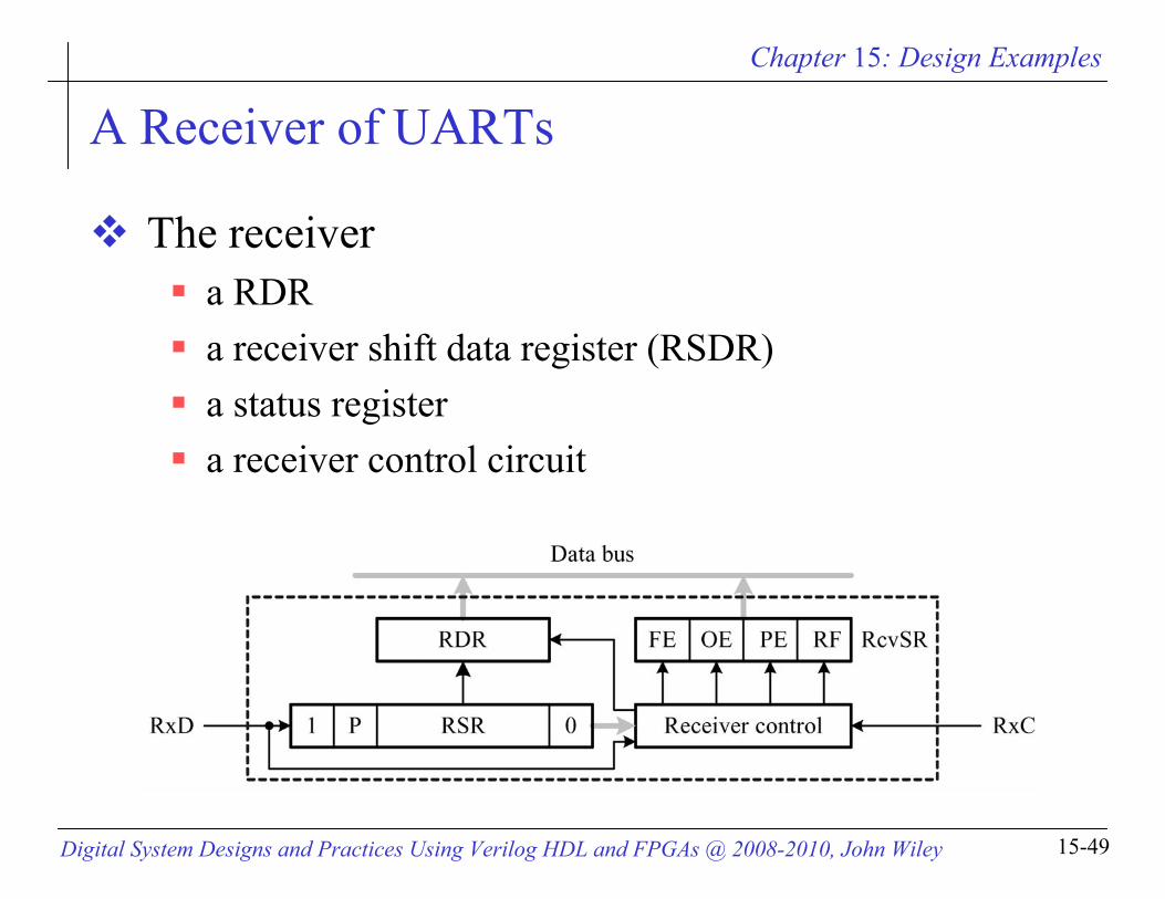
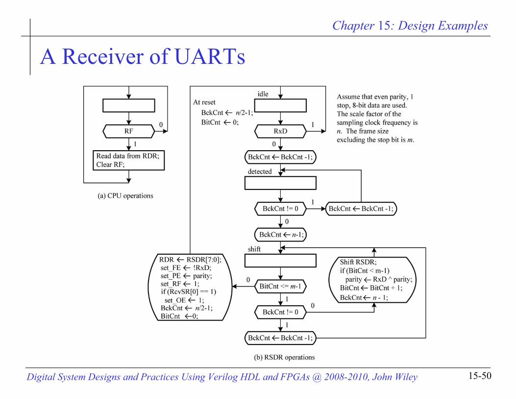
A Receiver of UARTs
The receivera RDRa receiver shift data register (RSDR)a status registera receiver control circuit
Chapter 15: Design Examples
Digital System Designs and Practices Using Verilog HDL and FPGAs @ 2008-2010, John Wiley 15-50
A Receiver of UARTs

Chapter 15: Design Examples
Digital System Designs and Practices Using Verilog HDL and FPGAs @ 2008-2010, John Wiley 15-51
Syllabus
ObjectivesBusData transferGeneral-purpose input and outputTimersUniversal asynchronous receiver and transmitter
InterfaceBasic transmitter structureBasic receiver structureBaud-rate generators
A simple CPU design

Chapter 15: Design Examples
Digital System Designs and Practices Using Verilog HDL and FPGAs @ 2008-2010, John Wiley 15-52
Baud-Rate Generators
The baud-rate generator provides TxC and RxC
Design approachesMultiplexer-based approachTimer-based approachOthers

Chapter 15: Design Examples
Digital System Designs and Practices Using Verilog HDL and FPGAs @ 2008-2010, John Wiley 15-53
Baud-Rate Generators

Chapter 15: Design Examples
Digital System Designs and Practices Using Verilog HDL and FPGAs @ 2008-2010, John Wiley 15-54
Syllabus
ObjectivesBusData transferGeneral-purpose input and outputTimersUniversal asynchronous receiver and transmitterA simple CPU design
Programming modelDatapath designControl unit design

Chapter 15: Design Examples
Digital System Designs and Practices Using Verilog HDL and FPGAs @ 2008-2010, John Wiley 15-55
CPU Basic Operations
Chapter 15: Design Examples
Digital System Designs and Practices Using Verilog HDL and FPGAs @ 2008-2010, John Wiley 15-56
The Software Model of CPU
The programming modelInstruction formatsAddressing modesInstruction set

Chapter 15: Design Examples
Digital System Designs and Practices Using Verilog HDL and FPGAs @ 2008-2010, John Wiley 15-57
The Programming Mode

Chapter 15: Design Examples
Digital System Designs and Practices Using Verilog HDL and FPGAs @ 2008-2010, John Wiley 15-58
Instruction Formats
Two major partsOpcodeOperand

Chapter 15: Design Examples
Digital System Designs and Practices Using Verilog HDL and FPGAs @ 2008-2010, John Wiley 15-59
Addressing Modes
The ways that operands are fetchedregister indexed register indirectimmediate

Chapter 15: Design Examples
Digital System Designs and Practices Using Verilog HDL and FPGAs @ 2008-2010, John Wiley 15-60
The Instruction Set
Double-operand instruction set

Chapter 15: Design Examples
Digital System Designs and Practices Using Verilog HDL and FPGAs @ 2008-2010, John Wiley 15-61
The Instruction Set
Single-operand instruction set
Chapter 15: Design Examples
Digital System Designs and Practices Using Verilog HDL and FPGAs @ 2008-2010, John Wiley 15-62
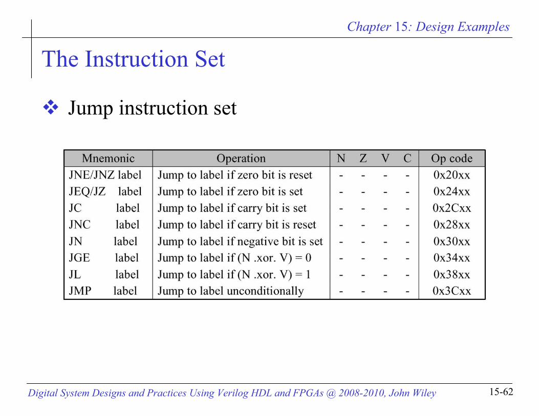
The Instruction Set
Jump instruction set

Chapter 15: Design Examples
Digital System Designs and Practices Using Verilog HDL and FPGAs @ 2008-2010, John Wiley 15-63
Syllabus
ObjectivesBusData transferGeneral-purpose input and outputTimersUniversal asynchronous receiver and transmitterA simple CPU design
Programming modelDatapath designControl unit design

Chapter 15: Design Examples
Digital System Designs and Practices Using Verilog HDL and FPGAs @ 2008-2010, John Wiley 15-64
A Datapath Design

Chapter 15: Design Examples
Digital System Designs and Practices Using Verilog HDL and FPGAs @ 2008-2010, John Wiley 15-65
ALU Functions

Chapter 15: Design Examples
Digital System Designs and Practices Using Verilog HDL and FPGAs @ 2008-2010, John Wiley 15-66
Syllabus
ObjectivesBusData transferGeneral-purpose input and outputTimersUniversal asynchronous receiver and transmitterA simple CPU design
Programming modelDatapath designControl unit design

Chapter 15: Design Examples
Digital System Designs and Practices Using Verilog HDL and FPGAs @ 2008-2010, John Wiley 15-67
A Control Unit
The decoder-based approach

Chapter 15: Design Examples
Digital System Designs and Practices Using Verilog HDL and FPGAs @ 2008-2010, John Wiley 15-68
A Control Unit
A better approach

Chapter 15: Design Examples
Digital System Designs and Practices Using Verilog HDL and FPGAs @ 2008-2010, John Wiley 15-69
A Control Unit
The operations of T3 and T4 are determined separately by each instruction


![MOAC Lesson 3. Any single letter, number, symbol, or punctuation mark. (John Wiley & Sons, Inc., 2014) Examples: C, ? 1 ]](https://img.pdfslide.us/doc/110x75/56649dca5503460f94ac0e84/moac-lesson-3-any-single-letter-number-symbol-or-punctuation-mark.jpg)