Embed Size (px)
Citation preview

Rev. 1.0 Sys MFG T/ED 4/25/2003
PC Architecture For Technicians Level-1Technical Excellence Development Series
Ch 14 - Page 1
Chapter 14Chapter 14PCI BUS Overview PCI BUS Overview PC Architecture for PC Architecture for
Technicians: LevelTechnicians: Level--11
Systems Manufacturing Training Systems Manufacturing Training and Employee Developmentand Employee Development
Copyright © 1996 Intel Corp.Copyright © 1996 Intel Corp.

Rev. 1.0 Sys MFG T/ED 4/25/2003
PC Architecture For Technicians Level-1Technical Excellence Development Series
Ch 14 - Page 2
OBJECTIVES: At the end of this section, the student will be able to do the following:
l Discuss Bus standards: ISA, EISA, VL BUS, & PCI
l Explain PCI Bus Architecture Fundamentals
l Discuss basic PCI bus cycles.
l Describe the Required PCI Bus signals.
l Discuss PCI Commands, Parity, Subtractive Decode, and PCI Arbitration
l Discuss the following as they relate PCI Configuration Access.
nPCI Configuration Registers; PCI Configuration Mechanism Type -1; PCI ID Select Line usage.

Rev. 1.0 Sys MFG T/ED 4/25/2003
PC Architecture For Technicians Level-1Technical Excellence Development Series
Ch 14 - Page 3
TheThePPeripheral eripheral
CComponent omponent IInterconnect nterconnect
BUSBUS

Rev. 1.0 Sys MFG T/ED 4/25/2003
PC Architecture For Technicians Level-1Technical Excellence Development Series
Ch 14 - Page 4
Why Local Bus?
Higher Performance, Higher Integration, and Low Cost
System Board
Memory
CPUCache
ExpansionBus I/F
CPUCache
Memory
System Board
PCI PCBasic PC
ExpansionBus Bridge
ISA / EISA /Micro Channel
MemoryController/Bridge
Add In
High BandwidthPCI Expansion
ModemFAX
ISA / EISA /Micro Channel
SCSI
AudioVGA
LANSCSI
Add In
VideoAudio
Modem
PCI Local Bus;PCI Local Bus;132 MBytes/Sec132 MBytes/SecLAN
Video
MemoryController
Graphics

Rev. 1.0 Sys MFG T/ED 4/25/2003
PC Architecture For Technicians Level-1Technical Excellence Development Series
Ch 14 - Page 5
IntroductionlThe ISA expansion bus in most of today’s PCs is
based on a design that is over a decade old.
lToday’s multitasking operating systems and feature rich applications require not only a faster processor but better throughput to system peripherals.nHigh Resolution Graphics Video Adapter
nFull Motion Video Adapter
nSCSI Host Bus Adapter
nNetwork Adapter

Rev. 1.0 Sys MFG T/ED 4/25/2003
PC Architecture For Technicians Level-1Technical Excellence Development Series
Ch 14 - Page 6
IntroductionlExpansion Bus Transfer Rate Limitations
nISA Bus Architecture3Transfers performed at 8/8.33 MHz clock speed.
316 bits data bus
38.33 MBytes/Sec Max. (2 bytes in 2 clocks)
nEISA Bus Architecture3Clock speed at 8/8.33 MHz
332 bits data bus
333 MBytes/Sec Max. (4 bytes in 1 clock)

Rev. 1.0 Sys MFG T/ED 4/25/2003
PC Architecture For Technicians Level-1Technical Excellence Development Series
Ch 14 - Page 7
IntroductionlThe PCI Bus Solution
nPCI Local Bus
3Peripheral Component Interconnect
3It is a high performance connection between motherboard components and expansion boards.
3Transfer Rate of 132 MBytes per second maximum with 32-bit bus implementation
3Transfer Rate of 264Mbytes per second with 64-bit bus implementation
35 volts and 3.3 volts Operation
3Clock Speed at 33 MHz or Less»66 MHz implemented in Rev 2.1 of PCI Spec for 3.3V only.

Rev. 1.0 Sys MFG T/ED 4/25/2003
PC Architecture For Technicians Level-1Technical Excellence Development Series
Ch 14 - Page 8
Bus Bus StandardsStandards

Rev. 1.0 Sys MFG T/ED 4/25/2003
PC Architecture For Technicians Level-1Technical Excellence Development Series
Ch 14 - Page 9
IntroductionThe following pages describe the numerous bus standards implemented in today’s Personal Computers.
What is a Bus?A bus is an electrical conduit in a computer that connects various components so they can communicate with each other. A bus standard is a set of rules that govern how the communications will take place....think of it as “grammar” for a computer. And different bus standards will have different grammatical rules that affect how quickly they can communicate.
Introduction - Bus Standards

Rev. 1.0 Sys MFG T/ED 4/25/2003
PC Architecture For Technicians Level-1Technical Excellence Development Series
Ch 14 - Page 10
PC Architecture Evolution
X86Processor
ISA, EISA, MicroChannelISA, EISA, MicroChannel
““Traditional PC”Traditional PC” ““PCI Local BusPCI Local Bus” PC” PC
Fax/Modem
X86Processor
ISA, EISA, ISA, EISA, MicroChannelMicroChannel
BusBus
FAST FAST access to memoryaccess to memoryFAST FAST access to I/Oaccess to I/O
Memory
Graphics Disk
System I/O System I/O
Memory
Fax/Modem
FASTFAST access to memoryaccess to memorySLOWER SLOWER access to I/Oaccess to I/O
Graphics Disk

Rev. 1.0 Sys MFG T/ED 4/25/2003
PC Architecture For Technicians Level-1Technical Excellence Development Series
Ch 14 - Page 11
ISAWhen the PC was introduced in the early 1980’s, the Industry Standard Architecture (ISA) bus was used. As the PC’s popularity spread and “clones” appeared, the ISA bus was always used for compatibility. It is 16-bits wide at 8MHz, and is fully compatible with all PC software. An ISA system will accept ISA add-in cards It is found in most PCs.
Page 2
CPUMemory
ISASlotsKeyboard, Disks,
Other Elements
ISA Bus
ISA Bus: Standard System
Introduction - Bus Standards

Rev. 1.0 Sys MFG T/ED 4/25/2003
PC Architecture For Technicians Level-1Technical Excellence Development Series
Ch 14 - Page 12
Introduction - Bus StandardsEISAThe Enhanced ISA, or EISA bus, is faster than ISA (32-bits @ 8MHz), and is fully compatible with ISA and all PC software. An EISA bus will give better overall performance to a computer system, and will accept ISA & EISA cards. It is typically used in servers, workstations and high-end PCs.
CPUMemory
EISASlotsKeyboard, Disks,
Other Elements
EISA Bus
EISA Bus: Improved overall performance
Rev. 1.0 Sys MFG T/ED 4/25/2003
PC Architecture For Technicians Level-1Technical Excellence Development Series
Ch 14 - Page 13
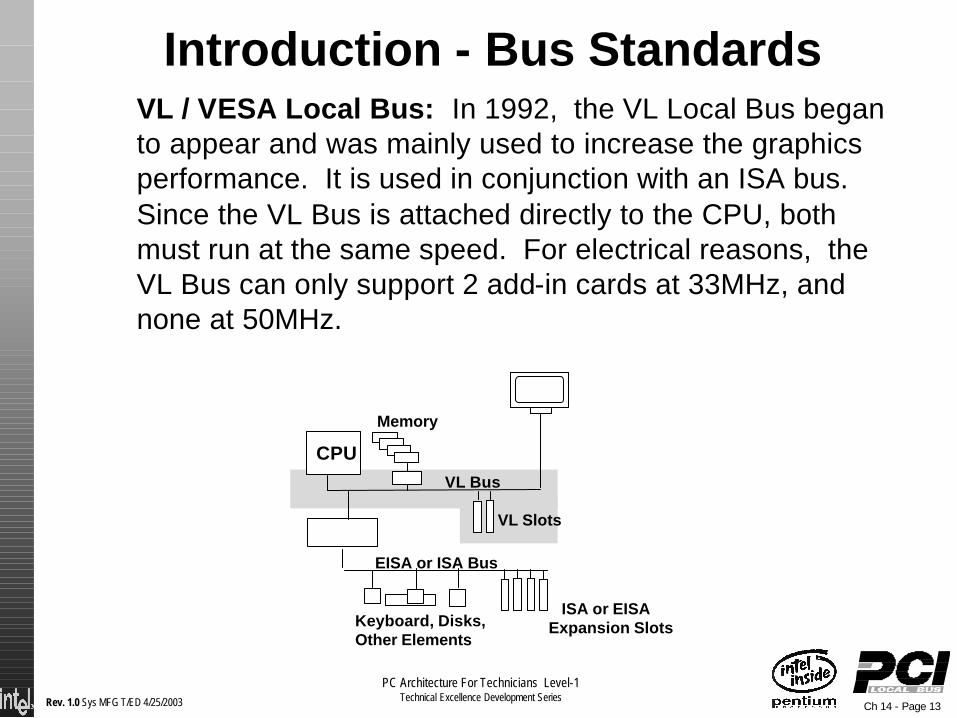
CPU
Memory
ISA or EISAExpansion SlotsKeyboard, Disks,
Other Elements
VL Slots
EISA or ISA Bus
VL Bus
VL / VESA Local Bus: In 1992, the VL Local Bus began to appear and was mainly used to increase the graphics performance. It is used in conjunction with an ISA bus. Since the VL Bus is attached directly to the CPU, both must run at the same speed. For electrical reasons, the VL Bus can only support 2 add-in cards at 33MHz, and none at 50MHz.
Introduction - Bus Standards

Rev. 1.0 Sys MFG T/ED 4/25/2003
PC Architecture For Technicians Level-1Technical Excellence Development Series
Ch 14 - Page 14
Page 3
CPU
Memory
ISA or EISAExpansion SlotsKeyboard, Disks,
Other Elements
EISA or ISA Bus
PCI Slots
PCI Bus
Disk, Networketc.
PCI Bus: Like the VL Bus, PCI will improve graphics performance, but will support other components as well (network, hard drive, etc.). Since it is not directly connected to the CPU, it sheds the electrical limitations of the VL bus and will accept multiple PCI-bus add-in cards.
Introduction - Bus Standards

Rev. 1.0 Sys MFG T/ED 4/25/2003
PC Architecture For Technicians Level-1Technical Excellence Development Series
Ch 14 - Page 15
PCI BUS PCI BUS ARCHITECTURE ARCHITECTURE
OVERVIEWOVERVIEW

Rev. 1.0 Sys MFG T/ED 4/25/2003
PC Architecture For Technicians Level-1Technical Excellence Development Series
Ch 14 - Page 16
PCI Bus TermsSee the Glossary at end of chapter for more definitions.
lAgent - Each PCI device, whether a bus master (initiator) or a target is referred to as a PCI Agent.
lBurst transfer - The basic PCI bus transfer mechanism which consists of 1 address phase & multiple data phases.
lConfiguration cycle - Bus cycles used for system initialization and configuration via the configuration address space.
lPCI - Peripheral Component Interconnect
lTransaction - An address phase plus one or more data phases.

Rev. 1.0 Sys MFG T/ED 4/25/2003
PC Architecture For Technicians Level-1Technical Excellence Development Series
Ch 14 - Page 17
Typical System Implementationl“Bridges” isolate buses electrically and logically.
lHigher performance functions on PCI.
lLow performance functions on (E)ISA, MC/A.
X86 CPU Cache MemorySubsystem
DRAM SubsystemPCI Bridge/Memory Controller
Host Bus
PCI Local Bus
PCI Add-in Slots
ISA BusBridge ISA Add-in Slots
ISA Bus
Rev. 1.0 Sys MFG T/ED 4/25/2003
PC Architecture For Technicians Level-1Technical Excellence Development Series
Ch 14 - Page 18
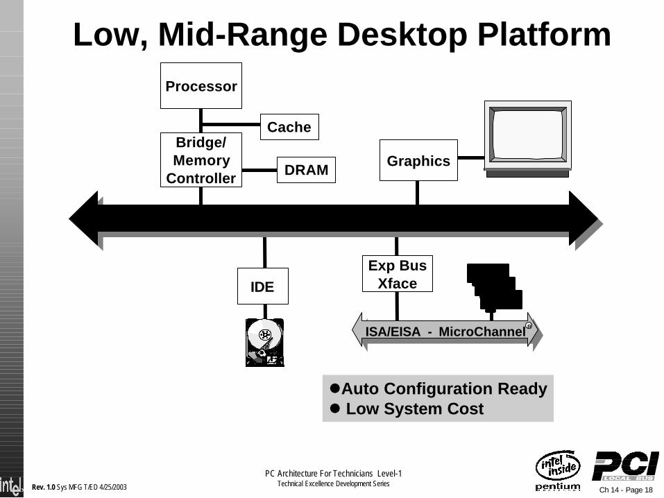
Low, Mid-Range Desktop Platform
lAuto Configuration Readyl Low System Cost
Exp BusXfaceIDE
Processor
Bridge/Memory
Controller DRAMGraphics
PCI Local Bus
ISA/EISA - MicroChannel
Cache
LAN
FaxModem
R

Rev. 1.0 Sys MFG T/ED 4/25/2003
PC Architecture For Technicians Level-1Technical Excellence Development Series
Ch 14 - Page 19
High-End Desktop Platform
l Scaleable PCI bus bandwidth - 64 bits addr & datalPerformance - linear burst; reads and writes
Exp BusXfaceLAN SCSI
Processor
Bridge/Memory
Controller
Audio
DRAM
MotionVideo
Graphics
PCI Local Bus
ISA/EISA - MicroChannel
Cache
Add-in
FaxModem
R

Rev. 1.0 Sys MFG T/ED 4/25/2003
PC Architecture For Technicians Level-1Technical Excellence Development Series
Ch 14 - Page 20
PCI MechanicallPCI defines “shared” slots.
lThe shared slot uses a different connector for the standard expansion card (e.g. ISA) and the PCI card.nComponents are mounted on
opposite side so both can use the same backplane area.
nCards are “mirrored” from ISA, EISA, and Micro Channel.
nExisting chassis do not require modification to accommodate PCI cards.
OR
Rev. 1.0 Sys MFG T/ED 4/25/2003
PC Architecture For Technicians Level-1Technical Excellence Development Series
Ch 14 - Page 21
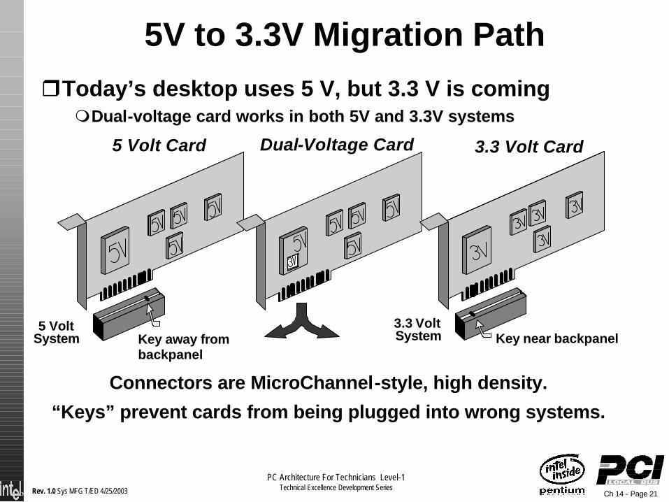
rToday’s desktop uses 5 V, but 3.3 V is comingmDual-voltage card works in both 5V and 3.3V systems
Connectors are MicroChannel-style, high density.
“Keys” prevent cards from being plugged into wrong systems.
5 Volt Card Dual-Voltage Card
Key away from5 Volt
Systembackpanel
3.3 Volt Card
Key near backpanel3.3 VoltSystem
5V to 3.3V Migration Path

Rev. 1.0 Sys MFG T/ED 4/25/2003
PC Architecture For Technicians Level-1Technical Excellence Development Series
Ch 14 - Page 22
Basic Electrical ConsiderationlThere are some unique electrical characteristics which
differentiate the PCI bus from other busses on the market today.
lMost bus specifications today employ the technique of Incident Wave Switching.nThis technique involves very strong output drivers that
are capable of driving the output node to a valid logic level in one voltage step.
nAs the signal propagates down the trace, each device it passes detects the logic level and is switched.
nLines are terminated at the physical end of the trace to minimize reflections.

Rev. 1.0 Sys MFG T/ED 4/25/2003
PC Architecture For Technicians Level-1Technical Excellence Development Series
Ch 14 - Page 23
l The PCI Specification utilizes Reflected Wave Switching.
nThis technique employs weaker output drivers that are only capable of driving the output node to half the voltage of a valid logic level.
nThe transition to a valid logic level occurs when the signal travels to the end of the unterminated (open) bus and is reflected.3The wave is reflected in phase with the incident wave,
effectively doubling the voltage on the bus.
3The wave is absorbed by the low impedance driver.
nGenerally speaking, each component is one load, each connector is one load, and the PCI card is one load.3An typical ChipSet can drive 10 PCI “loads”.
Basic Electrical Consideration

Rev. 1.0 Sys MFG T/ED 4/25/2003
PC Architecture For Technicians Level-1Technical Excellence Development Series
Ch 14 - Page 24
PCI BUS PCI BUS CYCLESCYCLES

Rev. 1.0 Sys MFG T/ED 4/25/2003
PC Architecture For Technicians Level-1Technical Excellence Development Series
Ch 14 - Page 25
PCI TransferPCI Transfer
lThe Initiator
lThe Target
lThe Agents
lThe PCI Bus Clock
lThe Address Phase
lClaiming the Transaction
lThe Data Phase
lTransactions Duration

Rev. 1.0 Sys MFG T/ED 4/25/2003
PC Architecture For Technicians Level-1Technical Excellence Development Series
Ch 14 - Page 26
PCI Transfer - Details to FollowAll signals are qualified by the system clock.

Rev. 1.0 Sys MFG T/ED 4/25/2003
PC Architecture For Technicians Level-1Technical Excellence Development Series
Ch 14 - Page 27
PCI TransferlThe PCI bus uses some multiplexed signals.
Examples are: nAD [31:0] - Multiplexed Address and Data bus.
3A typical bus cycle consists of one address phase and multiple data phases.
3During the address phase, the signals carry the start Address.
3During the data phase these signals carry the data objects being transferred between the initiator and target..
nC/BE [3:0]# - Bus Commands & Byte Enables.3During the address phase, the signals represent Bus
Commands
3During the data phase these represent Byte Enable signals.
Rev. 1.0 Sys MFG T/ED 4/25/2003
PC Architecture For Technicians Level-1Technical Excellence Development Series
Ch 14 - Page 28
PCI TransferlPCI Bus Clock - This is a synchronous bus.
nThe frequency of the CLK in PCI may be anywhere from 0MHZ to 33MHz. 366MHz implemented in Rev 2.1 of PCI Bus Specification for
3.3V cards only.
lTwo participants in every PCI burst transfer.nThe Initiator
3It is the device that initiates a transfer.
nThe Target3It is the device currently addressed by the initiator for the
purpose of performing a data transfer.

Rev. 1.0 Sys MFG T/ED 4/25/2003
PC Architecture For Technicians Level-1Technical Excellence Development Series
Ch 14 - Page 29
PCI TRANSFERlThe Address Phase
nEvery transaction starts off with an address phase one PCI CLK period in duration.
nDuring the address phase, the initiator identifies the target device (Address) and the type of transaction (Command - I/O or Memory Read / Write / Cfg).
lClaiming the TransactionnWhen a PCI agent determines that is the target of a
transaction, it must claim the transaction by asserting a PCI signal intended for this purpose (DEVSEL#).
nIf the initiator doesn’t see this signal asserted within a predetermined amount of time, it will abort the transaction. (No system hang if target not ready)

Rev. 1.0 Sys MFG T/ED 4/25/2003
PC Architecture For Technicians Level-1Technical Excellence Development Series
Ch 14 - Page 30
PCI TransferlThe Data Phase
nIt is the period during which a data object is transferred between the initiator and target.3Transfer when both the Initiator & Target are “READY”
nThe amount of data to be transferred is determined by the Commands/Bytes Enable signals that are set active by the initiator during the data phase.
nBoth the initiator and the target must indicate that they are ready to complete a data phase or the data phase will be extended by a wait state of one or more clock periods.3Wait states are inserted when either the Initiator or the
Target are “NOT READY”

Rev. 1.0 Sys MFG T/ED 4/25/2003
PC Architecture For Technicians Level-1Technical Excellence Development Series
Ch 14 - Page 31
PCI TransferlTransaction Duration
nThe initiator identifies the overall duration of a burst transfer with a framing signal (FRAME#).3This PCI signal is asserted at the start of the address phase
and remains active until the last data phase.
nThe PCI Spec allows PCI masters to burst indefinitely as long as the target can provide or accept the data and there are no other requests for the bus.
nA Master Latency Timer (MLT) ensures that the current bus master will not hog the bus if the arbitrator indicates that another PCI master is requesting access to the bus.3The MLT also guarantees the current bus master a
minimum amount of time before it must surrender the bus.

Rev. 1.0 Sys MFG T/ED 4/25/2003
PC Architecture For Technicians Level-1Technical Excellence Development Series
Ch 14 - Page 32
Basic Bus CyclelThe most fundamental PCI transfer mechanism is
the burst cycle
lFor a standard bus cycle, there must be a one to one correspondence between the number of addresses and the number of data transfers on the bus.nThere must be one address for every data item.
lA burst cycle is different from a standard cycle in that the burst cycle contains one address phase and multiple data phases.nIn a multiple-data phase transaction, it is the
responsibility of the target to latch the start address and manage the address from data phase to data phase.

Rev. 1.0 Sys MFG T/ED 4/25/2003
PC Architecture For Technicians Level-1Technical Excellence Development Series
Ch 14 - Page 33
Basic Bus CyclelThe motivation behind the concept of the burst cycle is
the Principle of Spatial Locality.n“If a item is referenced, nearby items will tend to be
referenced soon.”
lA simple illustration of this principle is the example of code fetching.nMost of the time these instructions will be located
sequentially in memory.
lBurst cycles generally only apply to memory cycles.nTypically I/O devices are not capable of burst cycles and
the Principle of Spatial Locality does not normally apply.

Rev. 1.0 Sys MFG T/ED 4/25/2003
PC Architecture For Technicians Level-1Technical Excellence Development Series
Ch 14 - Page 34
32-Bit Read Operation
4 bytes in 3 clks44 MBytes/s
All signals are qualified by the system clock.

Rev. 1.0 Sys MFG T/ED 4/25/2003
PC Architecture For Technicians Level-1Technical Excellence Development Series
Ch 14 - Page 35
Basic Read CyclelThe Cycle begins with the assertion of the
FRAME# signal in clock 1.nThis part of the cycle is termed the ADDRESS PHASE.
nAn address is presented on the AD[31:0] bus 3The address is latched by the target on the rising edge of
clock 2.
nA valid command is placed on the C/BE# lines.
3Example commands are: »Mem Read»I/O Write»Configuration Read

Rev. 1.0 Sys MFG T/ED 4/25/2003
PC Architecture For Technicians Level-1Technical Excellence Development Series
Ch 14 - Page 36
Basic Read CyclelAfter the address phase, there is a turnaround cycle
(i.e dead cycle) (clock 2) required to prevent bus contention when one agent stops driving a signal and another agent begins.nThis cycle allows the master to stop driving the address
on the bus, the output buffers on the master must be tristated by this time
nAD bus ownership changes from initiator to target.
nA turnaround cycle must last one clock and is required on all signals that may be driven by more than one agent.
nThe turnaround cycle is the clock between IRDY# asserted active and TRDY# asserted active.

Rev. 1.0 Sys MFG T/ED 4/25/2003
PC Architecture For Technicians Level-1Technical Excellence Development Series
Ch 14 - Page 37
Basic Read CyclelThe data phase begins on clock 3 when IRDY# is
driven active.nIRDY# is asserted during a read to indicate that the
initiator is ready to accept data from the currently-addressed target.
lThe target asserts the DEVSEL# signal during clock 3 to indicate that it has internally decoded the address and is responsible for the current bus cycle.
lWhen the target has output valid data, it asserts the TRDY# signal, telling the master that valid data is on the bus.nThe earliest time the target can provide data is in clock 4.

Rev. 1.0 Sys MFG T/ED 4/25/2003
PC Architecture For Technicians Level-1Technical Excellence Development Series
Ch 14 - Page 38
The data phase (Cont.)
lData transferred when both TRDY# & IRDY# are low.
lWait states are inserted by holding the assertion of the TRDY# signal.
lThe master can also insert wait states by driving the IRDY# signal inactive.
lFRAME# is deasserted on the cycle immediately previous to the cycle in which the final data item is latched by the master. (The next data transfer is the last).
lThe cycle is concluded when both FRAME# and IRDY# are deasserted.
Basic Read Cycle

Rev. 1.0 Sys MFG T/ED 4/25/2003
PC Architecture For Technicians Level-1Technical Excellence Development Series
Ch 14 - Page 39
32-Bit Write OperationNotice that no Turnaround Cycle is required
4 bytes in 2 clks66 MBytes/s

Rev. 1.0 Sys MFG T/ED 4/25/2003
PC Architecture For Technicians Level-1Technical Excellence Development Series
Ch 14 - Page 40
lThe write transaction begins with the assertion of FRAME# signal in clock 2.nThis is very much like a Read Cycle.
nFor a write is important to notice that no turnaround cycle is required because the master will continue to drive the bus with valid data signals on the next data phase.
nNotice that if IRDY# & TRDY# are both asserted for more than one clock cycle then new valid data is latched by the target on every clock cycle that both signals are asserted. 3Continuous bursting with no wait states.
3This applies to Read Cycles also.
Basic Write Cycle
Rev. 1.0 Sys MFG T/ED 4/25/2003
PC Architecture For Technicians Level-1Technical Excellence Development Series
Ch 14 - Page 41
PCI Signal PCI Signal DefinitionDefinition

Rev. 1.0 Sys MFG T/ED 4/25/2003
PC Architecture For Technicians Level-1Technical Excellence Development Series
Ch 14 - Page 42
PCI Signal DefinitionPCI Signal Definition
A minimal PCI master interface takes only 47 pins.

Rev. 1.0 Sys MFG T/ED 4/25/2003
PC Architecture For Technicians Level-1Technical Excellence Development Series
Ch 14 - Page 43
Signal Name Pin Pin Signal Name Signal Name Pin Pin Signal Name
GND A1 B1 -12V AD16 A32 B32 AD17+12V A2 B2 No Connect 3.3V A33 B33 CBE2 #
No Connect A3 B3 GND FRAME # A34 B34 GNDNo Connect A4 B4 No Connect GND A35 B35 IRDY #
Vcc A5 B5 Vcc TRDY # A32 B32 3.3VPCIINT3 # A6 B6 Vcc GND A37 B37 DEVSEL #PCIINT1 # A7 B7 PCIINT2 # STOP # A38 B38 GND
Vcc A8 B8 PCIINT4 # 3.3V A39 B39 PLOCK #Reserved A9 B9 No Connect SDONE A40 B40 PERR #
Vcc A10 B10 Reserved SBO # A41 B41 3.3VReserved A11 B11 No Connect GND A42 B42 SERR #
GND A12 B12 GND PAR A43 B43 3.3VGND A13 B13 GND AD15 A44 B44 CBE1 #
Reserved A14 B14 Reserved 3.3V A45 B45 AD14SPCIRST # A15 B15 GND AD13 A46 B46 GND
Vcc A16 B16 PCLKE AD11 A47 B47 AD12AGNT # A17 B17 GND GND A48 B48 AD10
GND A18 B18 REQA # AD9 A49 B49 GNDReserved A19 B19 Vcc KEY A50 B50 KEY
AD30 A20 B20 AD31 KEY A51 B51 KEY3.3V A21 B21 AD29 CBEO # A52 B52 AD8AD28 A22 B22 GND 3.3V A53 B53 AD7AD26 A23 B23 AD27 AD6 A54 B54 3.3VGND A24 B24 AD25 AD4 A55 B55 AD5AD24 A25 B25 3.3V GND A56 B56 AD3IDSEL A26 B26 CBE3 # AD2 A57 B57 GND3.3V A27 B27 AD23 AD0 A58 B58 AD1AD22 A28 B28 GND Vcc A59 B59 VccAD20 A29 B29 AD21 SREQ64 # A60 B60 SACK64 #GND A30 B30 AD19 Vcc A61 B61 VccAD18 A31 B31 3.3V Vcc A62 B62 Vcc
PCI
Connector
B49 M66ENOn 3.3V Cards
5v
Board

Rev. 1.0 Sys MFG T/ED 4/25/2003
PC Architecture For Technicians Level-1Technical Excellence Development Series
Ch 14 - Page 44
PCI Signal DefinitionPCI Signal DefinitionlPCI Signals - Required Pins (System)
nRST# - PCI Reset Signal (Asynchronous)3Forces all PCI configuration registers & output drivers to an
initialized state.
3All PCI signals in general should be driven to their benign states when RST# is activate.
»In general this means they must be tri-stated.»Implemented in the platform support logic (i.e, the chip
set [ e.g. 82371FB PIIX])

Rev. 1.0 Sys MFG T/ED 4/25/2003
PC Architecture For Technicians Level-1Technical Excellence Development Series
Ch 14 - Page 45
lPCI Signals - Required Pins (System)nCLK- PCI Clock Signal
3The PCI Clock Signal provides timing for all transactions, including bus arbitration's.
3All inputs to PCI devices are sampled on the rising edge of the CLK signal (0-1 transition).
3The frequency may be anywhere between 0MHz & 66MHz.»66MHz implemented in Rev 2.1 of PCI Bus Specification
for 3.3V cards only.»New Pin (M66EN) added to implement 66 MHz which is
grounded by all 33 MHz 3.3V cards»If M66EN is a logic 0, the Max. CLK frequency is 33
MHz.»If M66EN is a logic 1, the Max. CLK frequency is 66
MHz.
PCI Signal DefinitionPCI Signal Definition

Rev. 1.0 Sys MFG T/ED 4/25/2003
PC Architecture For Technicians Level-1Technical Excellence Development Series
Ch 14 - Page 46
PCI Signal DefinitionPCI Signal DefinitionlPCI Signals - Required Pins (Address/Data Bus)
nAD[31:0] - Multiplexed Address and Data bus.3A typical bus cycle consists of one address phase and
multiple data phases.
3During the address phase, the signals carry the start Address.
3During the data phase these signals carry the data objects being transferred between the initiator and target.
nC/BE[3:0]#-Multiplexed Bus Command/Bytes Enables3Defines the type of transaction.
3Represent Bus Commands during the address phase.
3Represent Byte Enable signals During the data phase.

Rev. 1.0 Sys MFG T/ED 4/25/2003
PC Architecture For Technicians Level-1Technical Excellence Development Series
Ch 14 - Page 47
PCI Signal DefinitionPCI Signal Definition
0 0 0 0 Interrupt Acknowledge0 0 0 1 Special Cycle0 0 1 0 I/O Read0 0 1 1 I/O Write0 1 0 0 Reserved0 1 0 1 Reserved0 1 1 0 Memory Data Read (1-15 Bytes)0 1 1 1 Memory Data Write (1-15 Bytes)1 0 0 0 Reserved1 0 0 1 Reserved1 0 1 0 PCI Configuration Read (IDSEL)1 0 1 1 PCI Configuration Write (IDSEL)1 1 0 0 Memory Data Read (96< Bytes)1 1 0 1 Dual Address Command (2 Cycles)1 1 1 0 Memory Data Read Line (16-95 Bytes)1 1 1 1 Memory Data Write and Invalidate
(Burst Writeback Cycle - 32< Bytes)
C3 C2 C1 C0
C/BE[3:0]# -Represent Bus Commands during the address phase

Rev. 1.0 Sys MFG T/ED 4/25/2003
PC Architecture For Technicians Level-1Technical Excellence Development Series
Ch 14 - Page 48
PCI Bus Parityl Generating address and data parity is required for PCI.
l Parity generation is delayed by one clock and error signalling is delayed by one more.

Rev. 1.0 Sys MFG T/ED 4/25/2003
PC Architecture For Technicians Level-1Technical Excellence Development Series
Ch 14 - Page 49
PCI Signal DefinitionPCI Signal DefinitionlPCI Signals - Required Pins (Address/Data Bus)
nPAR (Even Parity) - Protects AD[31:0] & C/BE#[3:0]3The computed PAR but must be set (or cleared) so that the
37-bit field consisting of AD[31:0] & C/BE#[3:0] and PAR contains an EVEN number of one bits.
3Driven by the initiator 1 clock after completion of the address phase and completion of each data phase of write transactions.
3Driven by the target 1 clock after completion of each data phase of read transactions.
3The computed Parity Bit is compared to the Parity Bit actually received on the PAR line to determine corruption.
»A Parity Error is reported on the PERR# Signal.

Rev. 1.0 Sys MFG T/ED 4/25/2003
PC Architecture For Technicians Level-1Technical Excellence Development Series
Ch 14 - Page 50
PCI Signal DefinitionPCI Signal DefinitionlPCI Signals - Required Pins (Interface Control )
nFRAME#3It indicates the start (when it is first asserted) and duration
(the duration of the assertion) of an access.
3FRAME# is deasserted when the initiator is ready to complete the final Data Phase.
»The next Data Transfer is the final Data Phase.
nTRDY# (Target Ready)3It is driven active when the target is ready to complete the
current data phase (data transfer).
3The data is transferred when the target is asserting TRDY# and the master is asserting IRDY#.

Rev. 1.0 Sys MFG T/ED 4/25/2003
PC Architecture For Technicians Level-1Technical Excellence Development Series
Ch 14 - Page 51
PCI Signal DefinitionPCI Signal DefinitionlPCI Signals - Required Pins (Interface Control )
nIRDY# (Initiator Ready)3During a write, it indicates that the initiator is driving valid
data onto the data bus.
3During a read, it indicates that the initiator is ready to accept data from the currently-addressed target.
nSTOP#3The target asserts STOP# to indicate that it wishes the
initiator to prematurely end the transfer in progress.
3This is a Target-Abort signal. »For example: Stop is asserted by the target if the target
can’t support the Burst request or if it takes more than 8 PCI clocks to complete the data phase.

Rev. 1.0 Sys MFG T/ED 4/25/2003
PC Architecture For Technicians Level-1Technical Excellence Development Series
Ch 14 - Page 52
lPCI can deal with targets with various address decode speeds.
l Extra address decode time (up to 2 clocks for medium & slow) allows varying price/performance designs.
l DEVSEL# timing is in Configuration Status Reg (Bit 10:9)
Target Device Select

Rev. 1.0 Sys MFG T/ED 4/25/2003
PC Architecture For Technicians Level-1Technical Excellence Development Series
Ch 14 - Page 53
PCI Signal DefinitionlPCI Signals - Required Pins (Interface Control )
nDEVSEL# - (Device Select)3It is an output driven active by a target when the target has
decoded its address.
3It is an input to the current master and used for a Master Abort if the initiator does not detect DEVSEL# within 6 clocks.
3It is an input to the Subtractive Decoder in the Expansion Bridge and used to claim the transaction if it does not detect DEVSEL# within 3 clocks (Fast, Med, Slow) after FRAME# is asserted.
»DEVSEL# is asserted by the Expansion Bridge during Clock 5 for Subtractive Decode.

Rev. 1.0 Sys MFG T/ED 4/25/2003
PC Architecture For Technicians Level-1Technical Excellence Development Series
Ch 14 - Page 54
Target Device Select (cont.)lSubtractive Address Decode
nCost effective mechanism to deal with a fragmented memory map. Only 1 agent can implement Subtractive Decode.
X86 CPU
PCI Bridge/Memory Controller
PCI Local Bus
Host Bus
ISA Bus
Address not claimedby PCI agent in 4 clocks
VGA
Access ToVGA Address
A000H
0H
C000H
10000H
VGA
640K
VGA BIOS
Empty
BIOS ROM
PCI Memory
HMA
Subtractive Decode Agent ISA BusBridge

Rev. 1.0 Sys MFG T/ED 4/25/2003
PC Architecture For Technicians Level-1Technical Excellence Development Series
Ch 14 - Page 55
Target Device Select (cont.)lSubtractive decoding definition.
nA method of address decoding in which a device accepts all accesses not positively decoded by another agents. 3Positive Decoding - A method of address decoding in
which a device responds to accesses only within an assigned address range.
lThe PCI-Expansion bus is designed to claim many transactions not claimed by other devices on the bus.nWhen a transaction is not claimed by any other PCI
device within a specified period of time, the PCI -Expansion bus bridge may assert DEVSEL# and pass the transaction through to the expansion bus ( e.g. ISA Bus)

Rev. 1.0 Sys MFG T/ED 4/25/2003
PC Architecture For Technicians Level-1Technical Excellence Development Series
Ch 14 - Page 56
PCI Configuration Cyclesl Each PCI Device (IC & Slot) has one IDSEL line.
nTypically upper address lines are connected to IDSEL signals.
IDSELLines
Rev. 1.0 Sys MFG T/ED 4/25/2003
PC Architecture For Technicians Level-1Technical Excellence Development Series
Ch 14 - Page 57
PCI Signal DefinitionlPCI Signals - Required Pins (Interface Control )
nIDSEL - Initialization Device Select3IDSEL is used as a PCI device chip select during
configuration read & write transactions.»Each PCI Device (IC & Slot) has one IDSEL line.
3Assertion of a specific IDSEL during the address phase of a configuration access is used to select the physical package that is the target of the configuration access.
3It is an Input for both Masters & Targets.
nNOTE: More information on IDSEL in section on PCI Configuration Access.

Rev. 1.0 Sys MFG T/ED 4/25/2003
PC Architecture For Technicians Level-1Technical Excellence Development Series
Ch 14 - Page 58
Signal DescriptionlPCI Signals - Required Pins (Error Reporting)
nPERR# (Parity Error)3Parity information is generated for all PCI devices that drive
address or data information onto the AD bus.
3A Parity Error is reported on the PERR# Signal if the computed Parity Bit does not compare to the Parity Bit actually received on the PAR line.
nSERR# (System Error)3This is considered a “last-recourse” for reporting serious
errors and typically causes an NMI.
3Is used to report address parity error, data parity error during a special cycle, problems other than parity detected by a PCI device.

Rev. 1.0 Sys MFG T/ED 4/25/2003
PC Architecture For Technicians Level-1Technical Excellence Development Series
Ch 14 - Page 59
Signal DescriptionlPCI Signals - Required Pins (Arbitration Signals)
Hidden Arbitration (Bus Masters Only)3Bus Arbitration can take place while another initiator is still
in control of the bus.
nREQ# (PCI Bus Request) Output3When an initiator requires the use of the PCI bus, it asserts
its device-specific REQ# line to the arbiter.
nGNT# (PCI Bus Grant) Input3When the arbiter has determined that the requesting initiator
should be granted control of the PCI bus, it asserts the GNT# (Grant) line specific to the requesting initiator.

Rev. 1.0 Sys MFG T/ED 4/25/2003
PC Architecture For Technicians Level-1Technical Excellence Development Series
Ch 14 - Page 60
PCI Bus ArbitrationBus arbitration is centralized.l Number of masters limited only by number of REQ# / GNT#
pairs supplied by the arbiter (e.g. 82437 TSC REQ#[3:0])
nArbitration method not specified (e.g. Rotating priority).
3“Fairness” algorithm is implemented by designer.
Potential Bus Masters
Arbiter
REQ# 1
REQ# 2
GNT# 1
GNT# 2
Bus Slave
PCI BUS

Rev. 1.0 Sys MFG T/ED 4/25/2003
PC Architecture For Technicians Level-1Technical Excellence Development Series
Ch 14 - Page 61
PCI Bus Arbitration (cont.)Arbitration cycles on the bus happen in parallel with the
current bus cycle (if any). No arbitration overhead.
Rev. 1.0 Sys MFG T/ED 4/25/2003
PC Architecture For Technicians Level-1Technical Excellence Development Series
Ch 14 - Page 62
PCI Bus Arbitration (cont.)lArbitration cycles on the bus happen in parallel with
the current bus cycle (if any). No arbitration overhead.
lEach bus master has it’s own request and grant signal, which are intercepted and used by the arbiter.
lThe PCI specification allows PCI masters to burst indefinitely so long as the target can provide or accept the data and no other agent wants the bus.
lThe PCI specification prevents slow targets from monopolizing the bus by requiring targets to retry if the transactions take longer than:nthe “16 clock rule” to complete the first data phase
nthe “8 clock rule” to complete the current data phase.

Rev. 1.0 Sys MFG T/ED 4/25/2003
PC Architecture For Technicians Level-1Technical Excellence Development Series
Ch 14 - Page 63
lEach master also has an associated Master Latency Timer (MLT) which determines the maximum number of PCI clocks that the master can be own the bus when another request is pending. nThe MLT is decremented by one on each PCI clock.
3Once the timer expires AND the GNT signal is deasserted, the master must initiate termination of the cycle.
nThe LT ensures that the current bus master will not hog the bus if the arbitrator indicates that another PCI master is requesting access to the bus.
nThe LT also guarantees the current bus master a minimum amount of time before it must surrender the bus.
PCI Bus Arbitration (cont.)

Rev. 1.0 Sys MFG T/ED 4/25/2003
PC Architecture For Technicians Level-1Technical Excellence Development Series
Ch 14 - Page 64
PCIPCIDEVICE DEVICE
CONFIGURATIONCONFIGURATION

Rev. 1.0 Sys MFG T/ED 4/25/2003
PC Architecture For Technicians Level-1Technical Excellence Development Series
Ch 14 - Page 65
PCI Device ConfigurationlAnother important aspect of the PCI specification is
the auto-configuration of PCI devices on the bus.
lWith ISA today, when a one adds a new I/O card to the PC, one must be aware of the I/O requirements of the card to be added.nTypically this involves setting jumpers and adjusting base
addresses and interrupts. (e.g. I/O = 340H, IRQ5)
lThe PCI specification requires that all devices must have a set of configuration registers that are examined upon power up.nJumpers and switches cannot be used for PCI
configuration.

Rev. 1.0 Sys MFG T/ED 4/25/2003
PC Architecture For Technicians Level-1Technical Excellence Development Series
Ch 14 - Page 66
PCI Device ConfigurationlUpon power up, the configuration software (probably
the BIOS) detects the presence of all PCI devices on the bus.nOnce detected, the software assesses the configuration
space of each device and assigns memory and I/O regions that are guaranteed not to be used by other PCI devices.3All the configuration will be performed automatically.
lThe visible results is that the end user merely powers down the PC, inserts the new card, and then powers up the PC.
3Plug-n-Play

Rev. 1.0 Sys MFG T/ED 4/25/2003
PC Architecture For Technicians Level-1Technical Excellence Development Series
Ch 14 - Page 67
PCI Configuration SpacePCI Configuration SpacelPCI Configuration Registers
n PCI devices implement a 256 byte space for Configuration Registers which provide a software interface for board and system set-up.3Organized as 64 DWord Registers
»64Dwords * 4 bytes/DWord = 256 bytes
nThe first 64 byte locations are predefined by the PCI specification.364 byte Header region -> 40H bytes (00H to 3FH)
nThe remaining 192 locations are device-specific.

Rev. 1.0 Sys MFG T/ED 4/25/2003
PC Architecture For Technicians Level-1Technical Excellence Development Series
Ch 14 - Page 68
lThese registers contain data items including:nVendor ID
38086H = Intel; 1002H = ATI
nDevice ID3122EH = 82371FB PIIX Fn 0; 4158H = MACH32 Video
nStatus Register
nCommand Register
nClass Code30601H= ISA Bridge; 0101H = IDE controller
nRevision ID 3Depends on stepping of device (e.g. - 01H).
PCI Device Configuration

Rev. 1.0 Sys MFG T/ED 4/25/2003
PC Architecture For Technicians Level-1Technical Excellence Development Series
Ch 14 - Page 69
PCI Configuration SpacePCI Configuration SpaceFormat of a PCI Device’s Configuration Header
R e s e r v e d
V endor IDDevice ID
L a t e n c yT im e r
B I S T
0151631
R e s e r v e d
R e s e r v e d
C o m m a n dS t a t u s
0
0
0
0
1
2
3
3
3
Re vision ID
1
1
1
2
2
2
3
0 h
4 h
8 h
C h
0 h
0 h
0 h
4 h
C h
4 h
8 h
C h
4 h
8 h
C h
8 h
C a c h e L in eS iz e
H e a d e rT y p e
I n te r r u p tL in eM a x _ L a t M in _ G n t
R e s e r v e d
I n te r r u p tP in
B a s e A d d r e s s R e g is t e r s
C lass C ode
E x p a n s i o n R O M B a s e A d d r e s s
00010203
24252627
3C3D3E3F

Rev. 1.0 Sys MFG T/ED 4/25/2003
PC Architecture For Technicians Level-1Technical Excellence Development Series
Ch 14 - Page 70
PCI Configuration SpacePCI Configuration SpacelFunctional Device’s Header Region
nVendor ID - Offset 00H & 01H (R/O register) 3Identifies the manufacturer of the device. (e.g. Intel)
nDevice ID - Offset 02H & 03H (R/O register) 3Assigned by the device manufacturer and identifies the type
of device (e.g. TSC, PIIX, MACH32 Video)
nCommand Register - Offset 04H & 05H (R/W register) 3Provides basic control over the device’s ability to respond to
PCI accesses. Used by BIOS.
nStatus Register - Offset 06H & 07H3Tracks the status of PCI bus-related events. Used by BIOS.

Rev. 1.0 Sys MFG T/ED 4/25/2003
PC Architecture For Technicians Level-1Technical Excellence Development Series
Ch 14 - Page 71
PCI Configuration SpacePCI Configuration SpacenRevision ID - Offset 08H (R/O register)
3Indicates Stepping of Device. Used by BIOS.
nBase Class Code - Offset 0BH (R/O register)»Base Class identifies the basic function.
»(e.g. Mass Storage; Display Controller)
3Examples of defined Class Codes are:»01H - Mass Storage; 02H - Network Controller: »03H - Display Controller; 04H - Multimedia Device.
nSub-Class Code - Offset 0AH (R/O register) »Sub-Class is more specific.
» (e.g. IDE controller; VGA controller)
Rev. 1.0 Sys MFG T/ED 4/25/2003
PC Architecture For Technicians Level-1Technical Excellence Development Series
Ch 14 - Page 72
PCI Configuration ExamplelThe PCI Configuration Address register is a 32-bit
register located at CF8H, the PCI Configuration Data register is a 32-bit register located at CFCh. n These registers are accessible by DWORD, WORD
or BYTE accesses
lHOW TO ACCESS I/O CONFIGURATION SPACE USING CONFIGURATION MECHANISM #1n1. Using a DWORD write command, output the
desired I/O configuration address to I/O port CF8H
n2. Using a DWORD read or write command, read or write data from the I/O port CFCH

Rev. 1.0 Sys MFG T/ED 4/25/2003
PC Architecture For Technicians Level-1Technical Excellence Development Series
Ch 14 - Page 73
PCI Configuration Example
nCONFIG SPACE ENABLE FLAG (Bit 31): Always 1 to indicate I/O access is to configuration space.
nRESERVED (Bits 30-24): Always 00h
nBUS NUMBER (Bits 23-16): Always 00h unless a bridge card is installed in a PCI slot
nDEVICE NUMBER (Bits 15-10): Used to indicate a specific PCI device. (e.g. The TSC, PIIX and PCI slots)
nFUNCTION NUMBER (Bits 10-8): PIIX is multi-function device.
nREGISTER NUMBER (Bits 7-0): Defines one of 64 DWORD locations for a specific PCI device. Note that Bits 1 and 0 must always be 0H (Zero Hex) for DWORD access.
31-30 24-23 16-15 8-7 2-1-011-10
Reserved RBus Number Dev # Register #1 FCNHOSTDATABUS

Rev. 1.0 Sys MFG T/ED 4/25/2003
PC Architecture For Technicians Level-1Technical Excellence Development Series
Ch 14 - Page 74
Using Mechanism - 1, Type 0
Accessing a PCI config. port is a 2 step process:3 Point & Shoot
l 1. Write the BUS#, DEV#, FCN# & REG# to CFG ADDR PORT
nPoint :> dport (0CF8) = CONE BUS# DEV# FCN# REG
ne.g. - dport (0CF8) = 8000xxxx; dport (0CF8) = 80003808
l 2. Perform an I/O read or write to the CFG DATA PORT.nShoot:> dport (0CfC)
ne.g. - dport (0CFC) [read] , dport (0CFC) = xxxxxxxx [write]
PCI Configuration Example31-30 24-23 16-15 8-7 2-1-011-10
Reserved RBus Number Dev # Register #1 FCNHOSTDATABUS

Rev. 1.0 Sys MFG T/ED 4/25/2003
PC Architecture For Technicians Level-1Technical Excellence Development Series
Ch 14 - Page 75
PCI Configuration Example
dport(0cf8)=80003800H 1000 0000 0000 0000 0011 1000 0000 0000
31-30 24-23 16-15 8-7 2-1-011-10
Reserved RBus Number Dev # Register #1 FCNHOSTDAT
ABUS
l0CF8h is the Configuration Address Port (Point)nMust be accessed using a full 32-bit write.
nBit 31 Cfg. Space Enable (CONE) must be set to a 1
nPoint to a Register in a specific Device with CF8H.CONE BUS# DEV# FCN# REG
dport (0CF8) = 80003800 (ITP example)
n32 BIT Port (0CF8) contains I/O Addr CF8, CF9, CFA, & CFB

Rev. 1.0 Sys MFG T/ED 4/25/2003
PC Architecture For Technicians Level-1Technical Excellence Development Series
Ch 14 - Page 76
PCI Configuration Examplel0CFCh is the Configuration Data Port (Shoot)
332 BIT Port (0CFC) contains I/O Addr CFC, CFD, CFE, & CFF
nRead or Write the Data at the address pointed to at CF8H.
nNOTE: Any address output to CF8h is always on a 4 byte (DWORD) boundary. 3ITP uses Dport for 4 bytes, Wport for 2 bytes, Port for 1 Byte
n You can read or write any DWORD, WORD, or BYTE in the four byte range by using the correct offset as follows:3DWORD @ CFCh
3WORD @ CFCh or CFEh
3BYTE @ CFCh, CFDh, CFEh or CFFh

Rev. 1.0 Sys MFG T/ED 4/25/2003
PC Architecture For Technicians Level-1Technical Excellence Development Series
Ch 14 - Page 77
PCI Configuration ExamplelExamples of Accessing PCI Configuration
Space using an ITP:
nRead Example:3dport (0CF8H) = 80000060H
3dport (0CFCH)
nWrite Example:3dport (0CF8H) = 80000060H
3dport (0CFCH) = 02020000H

Rev. 1.0 Sys MFG T/ED 4/25/2003
PC Architecture For Technicians Level-1Technical Excellence Development Series
Ch 14 - Page 78
PCI Configuration Cyclesl Typically upper address lines are connected to IDSEL signals.
l Newer Devices use AD11-31, Older Devices used AD16-31.
Each PCI Device (IC & Slot) has one IDSEL line.
IDSELLines

Rev. 1.0 Sys MFG T/ED 4/25/2003
PC Architecture For Technicians Level-1Technical Excellence Development Series
Ch 14 - Page 79
PCI Configuration Cyclesl IDSEL is used as a PCI device chip select during
configuration read & write transactions.nAssertion of a specific IDSEL during the address phase of a
configuration access is used to select the physical package that is the target of the configuration access.
l Each PCI Device (IC & Slot) has one IDSEL line.
Example implementation follows:nThe IDSEL associated with device 0 is connected to AD11
nThe IDSEL associated with device 1 is connected to AD12 etc.
nThe IDSEL associated with device 7 is connected to AD18.
nThe IDSEL associated with device 20 is connected to AD31.
3Note: The Host Bridge is always Device #0 & does not pass it Cfg cycles to the PCI bus, thus AD11 is never asserted.

Rev. 1.0 Sys MFG T/ED 4/25/2003
PC Architecture For Technicians Level-1Technical Excellence Development Series
Ch 14 - Page 80
IDSEL: 1 line set high by Bridge Device based on decoding of the target’s physical Device number contained in Config Address bits 15:11 (DEV#) (Newer Devices use AD11-31)
PCI Config. Cycles: Mechanism-1, Type 0
31-30 24-23 16-15 8-7 2-1-011-10
Reserved RBus Number Dev # Register #1 FCN
31 8-7 2-1-011-10
00Register #FCN"IDSEL" Alias - Only 1 bit set!PCIA/DBUS
HOSTDATABUS
AD18
[e.g. dport(0cf8)=80003800H: Dev #7 -> AD18]1000 0000 0000 0000 0011 1000 0000 0000

Rev. 1.0 Sys MFG T/ED 4/25/2003
PC Architecture For Technicians Level-1Technical Excellence Development Series
Ch 14 - Page 81
I/O Cfg Addr -> Device Number Mapping
78XX F AD26 0111 1 000 XXXX XX00
ADDR
00XX
08XX
10XX
18XX
0000
0000
0001
0001
0010
0010
0011
0011
0100
0100
0101
0101
0110
0110
0111
000
000
000
000
000
000
000
000
000
000
000
000
000
000
000
XXXX XX00
XXXX XX00
XXXX XX00
XXXX XX00
XXXX XX00
XXXX XX00
XXXX
XXXX
XXXX
XXXX
XXXX
XX00
XX00
XX00
XX00
XX00
XX00
XX00
XX00
XX00
XXXX
XXXX
XXXX
XXXX
20XX
28XX
30XX
Dev # IDSEL 15,14,13,12 11
Device # FCN
10, 9, 8 7,6,5,4 3,2,1,0
Register #
0 AD11
1 AD12
2 AD13
0
1
0
3 AD14 1
4 AD15 0
5 AD16 1
6 AD17 0
38XX
40XX
48XX
50XX
58XX
60XX
68XX
70XX
7
8
9
A
B
C
D
E
AD18
AD19
AD20
AD21
AD22
AD23
AD24
AD25
1
0
1
0
1
0
1
0
D 15:0
Newer Devices use AD11-31
Lower 16 bits of Host
Data Bus

Rev. 1.0 Sys MFG T/ED 4/25/2003
PC Architecture For Technicians Level-1Technical Excellence Development Series
Ch 14 - Page 82
PCI Config. Cycles: Mechanism-1, Type 0
31-30 24-23 16-15 8-7 2-1-011-10
Reserved RBus Number Dev # Register #1 FCN
31 8-7 2-1-011-10
00Register #FCN"IDSEL" Alias - Only 1 bit set!
16-15
RPCIA/DBUS
HOSTDATABUS
IDSEL: 1 line set high by Bridge Device based on decoding of the target’s physical Device number contained in Config Address bits 15:11 (DEV#) (Older Devices use AD16-31)
[e.g. dport(0cf8)=80003900H: Dev #7 -> AD23]1000 0000 0000 0000 0011 1001 0000 0000
AD23

Rev. 1.0 Sys MFG T/ED 4/25/2003
PC Architecture For Technicians Level-1Technical Excellence Development Series
Ch 14 - Page 83
I/O Cfg Addr -> Device Number Mapping
78XX F AD31 0111 1 000 XXXX XX00
ADDR
00XX
08XX
10XX
18XX
0000
0000
0001
0001
0010
0010
0011
0011
0100
0100
0101
0101
0110
0110
0111
000
000
000
000
000
000
000
001
000
000
000
000
000
000
000
XXXX XX00
XXXX XX00
XXXX XX00
XXXX XX00
XXXX XX00
XXXX XX00
XXXX
XXXX
XXXX
XXXX
XXXX
XX00
XX00
XX00
XX00
XX00
XX00
XX00
XX00
XX00
XXXX
XXXX
XXXX
XXXX
20XX
28XX
30XX
Dev # IDSEL 15,14,13,12 11
Device # FCN
10, 9, 8 7,6,5,4 3,2,1,0
Register #
0 AD16
1 AD17
2 AD18
0
1
0
3 AD19 1
4 AD20 0
5 AD21 1
6 AD22 0
39XX
40XX
48XX
50XX
58XX
60XX
68XX
70XX
7
8
9
A
B
C
D
E
AD23
AD24
AD25
AD26
AD27
AD28
AD29
AD30
1
0
1
0
1
0
1
0
D15:0
Older Devices used AD16-31
Lower 16 bits of Host
Data Bus

Rev. 1.0 Sys MFG T/ED 4/25/2003
PC Architecture For Technicians Level-1Technical Excellence Development Series
Ch 14 - Page 84
Where to get more informationlPCI Local Bus Specification (PCI SIG)
nPCI Special Interest Group (CC:Mail PCI_SIG)
lPCI System Architecture (Shanley & Anderson)nMindshare (ISBN 0-201-40993-3)
lThe Indispensable PC Hardware Book (Messmer)nAddison-Wesley (ISBN 0-201-87697-3)
lPCI Hardware and Software (Solari & Willse)nAnnabooks (ISBN 0-929392-28-0)

Rev. 1.0 Sys MFG T/ED 4/25/2003
PC Architecture For Technicians Level-1Technical Excellence Development Series
Ch 14 - Page 85
GLOSSARYGLOSSARY

Rev. 1.0 Sys MFG T/ED 4/25/2003
PC Architecture For Technicians Level-1Technical Excellence Development Series
Ch 14 - Page 86
PCI Bus GlossarylAgent
nEach PCI device, whether a bus master (initiator) or a target is referred to as a PCI Agent.
nA logical entity that operates on a computer bus. The term applies collectively to functions of a bus master or a bus slave, or to a combination of both.
lBridgenThe logic that connects one computer to another,
allowing an agent on one bus to access an agent on the other.
nExamples would be the bridge between the PCI bus and a standard expansion bus (e.g. ISA bus)
Rev. 1.0 Sys MFG T/ED 4/25/2003
PC Architecture For Technicians Level-1Technical Excellence Development Series
Ch 14 - Page 87
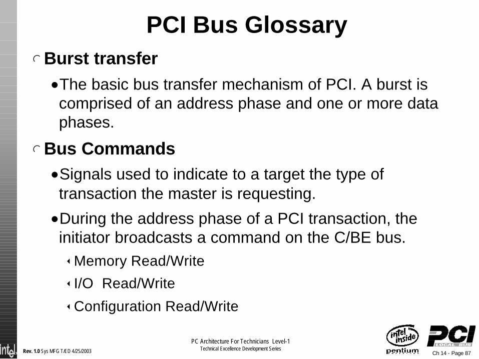
lBurst transfernThe basic bus transfer mechanism of PCI. A burst is
comprised of an address phase and one or more data phases.
lBus CommandsnSignals used to indicate to a target the type of
transaction the master is requesting.
nDuring the address phase of a PCI transaction, the initiator broadcasts a command on the C/BE bus.3Memory Read/Write
3I/O Read/Write
3Configuration Read/Write
PCI Bus Glossary

Rev. 1.0 Sys MFG T/ED 4/25/2003
PC Architecture For Technicians Level-1Technical Excellence Development Series
Ch 14 - Page 88
lBus device - A bus device can be either a bus master or target:nMASTER
3An agent which has an ability to obtain control of the interface and perform memory or I/O reads and writes to system resources.
3Drives the address phase, and transaction boundary (FRAME#). The master initiates a transaction, drives the data handshaking signal (IRDY#) with the target.
nTARGET - Claims the transaction by asserting DEVSEL# and handshakes the transaction (TRDY#) with the initiator.
PCI Bus Glossary

Rev. 1.0 Sys MFG T/ED 4/25/2003
PC Architecture For Technicians Level-1Technical Excellence Development Series
Ch 14 - Page 89
lConfiguration address spacenA set of 64 registers (DWORDS) used for configuration,
initialization, and catastrophic error handling. This address space consists of two regions: a header region and a device-dependent region.
lConfiguration cyclenBus cycles used for system initialization and
configuration via the configuration address space.
lLatency timernA mechanism for ensuring that a bus master does not
extend the access latency of other masters beyond a specified value.
PCI Bus Glossary

Rev. 1.0 Sys MFG T/ED 4/25/2003
PC Architecture For Technicians Level-1Technical Excellence Development Series
Ch 14 - Page 90
lPCI - Peripheral Component Interconnect.
lPhase - One or more clocks in which a single unit of information is transferred, consisting of:nAn address phase (a single address transfer in one clock
for a single address cycle and two clocks for a dual address cycle).
nA data phase (one transfer state plus zero or more wait states).
lPositive DecodingnA method of address decoding in which a device
responds to accesses only within an assigned address range. See also subtractive decoding.
PCI Bus Glossary

Rev. 1.0 Sys MFG T/ED 4/25/2003
PC Architecture For Technicians Level-1Technical Excellence Development Series
Ch 14 - Page 91
lSubtractive decodingnThe PCI-Expansion bus is designed to claim many
transactions not claimed by other devices on the bus.
nA method of address decoding in which a device accepts all accesses not positively decoded by another agents. See also positive decoding.
lTargetnAn agent that responds (with a positive acknowl-
edgement by asserting DEVSEL#) to a bus transaction initiated by a master.
lTransactionnAn address phase plus one or more data phases.
PCI Bus Glossary

Rev. 1.0 Sys MFG T/ED 4/25/2003
PC Architecture For Technicians Level-1Technical Excellence Development Series
Ch 14 - Page 92
lTurnaround cycle nA bus cycle used to prevent contention when one agent
stops driving a signal and another agent begins. A turnaround cycle must last one clock and is required on all signals that may be driven by more than one agent.
lWait StatenA bus clock in which no transfer occurs.
PCI Bus Glossary
Rev. 1.0 Sys MFG T/ED 4/25/2003
PC Architecture For Technicians Level-1Technical Excellence Development Series
Ch 14 - Page 93
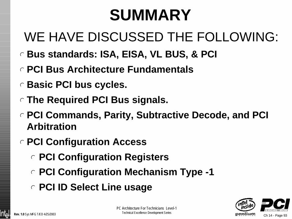
SUMMARYWE HAVE DISCUSSED THE FOLLOWING:
l Bus standards: ISA, EISA, VL BUS, & PCI
l PCI Bus Architecture Fundamentals
l Basic PCI bus cycles.
l The Required PCI Bus signals.
l PCI Commands, Parity, Subtractive Decode, and PCI Arbitration
l PCI Configuration Access
l PCI Configuration Registers
l PCI Configuration Mechanism Type -1
l PCI ID Select Line usage


![APPENDIX D. BINARY-DECIMAL-HEXADECIMAL CONVERSION …faculty.chemeketa.edu/csekafet/ELT253/8085/... · Appendix D. Binary-Decimal·Hexadecimal Conver,jot] Tables . HEXADECIMAL-DECIMAL](https://img.pdfslide.us/doc/110x75/5ea5c10874b2b667df42579d/appendix-d-binary-decimal-hexadecimal-conversion-appendix-d-binary-decimalhexadecimal.jpg)


![PCArch-full course-description.ppt [Read-Only]faculty.chemeketa.edu/csekafet/ELT256/PCArch-full_co… · · 2015-01-14PCI commands, Parity, Subtractive Decode, and PCI ... Components](https://img.pdfslide.us/doc/110x75/5b05d87b7f8b9abf568c2b3c/pcarch-full-course-read-onlyfacultychemeketaeducsekafetelt256pcarch-fullco2015-01-14pci.jpg)