Embed Size (px)
Citation preview

Chapter 11Digital Data Transmission byBaseband Pulse AmplitudeModulation (PAM)
Contents
Slide 1 Pulse Amplitude Modulation (PAM)Slide 2 Block Diagram of PAM SystemSlide 3 PAM Block Diagram DescriptionSlide 4 Block Diagram Description (cont. 1)Slide 5 Block Diagram Description (cont. 2)Slide 6 Block Diagram Description (cont. 3)Slide 7 Intersymbol Interference (ISI)Slide 8 Eye DiagramsSlide 10 Formula for Eye ClosureSlide 11 Nyquist Criterion for No ISISlide 12 Nyquist’s Criterion (cont.)Slide 13 Raised Cosine Shaping FiltersSlide 14 Raised Cosine Filters (cont.)Slide 15 Splitting the ShapingSlide 16 Interpolation Filter BankSlide 17 Interpolation Filter Bank (cont.)Slide 18 Symbol Error Probability vs. SNR
Slide 19 Example Filter Bank for L = 2Slide 20 Symbol Error Probability (2)Slide 21 Symbol Error Probability (3)Slide 22 Symbol Error Probability (4)Slide 23 Symbol Error Probability (5)Slide 24 Symbol Error Probability (6)Slide 24 Generating a Symbol Clock ToneSlide 25 Generating a Clock Tone (cont. 1)Slide 26 Generating a Clock Tone (cont. 2)Slide 27 Generating a Clock Tone (cont. 3)Slide 28 Generating a Clock Tone (cont. 4)Slide 29 Generating a Clock Tone (cont. 5)Slide 30 Generating a Clock Tone (cont. 6)
Slide 31 Theoretical ExercisesSlide 32 Theoretical Exercises (cont. 1)Slide 33 Theoretical Exercises (cont. 2)Slide 34 Theoretical Exercises (cont. 3)Slide 35 Theoretical Error ProbabilitySlide 36 Theoretical Exercises (cont. 4)Slide 37 Making a PAM SignalSlide 38 Frequency Response of the
Shaping FilterSlide 39 Using a Mailbox for OutputsSlide 40 Using a Mailbox (cont.)Slide 41 Generating a Baud Synch Signal

Slide 42 Making a Clock Tone GeneratorSlide 43 Making a Tone Generator (cont.)Slide 43 Testing the Tone GeneratorSlide 44 Testing the Generator (cont. 1)Slide 45 Testing the Generator (cont. 2)Slide 46 Optional Team ExerciseSlide 47 Optional Team Exercise (cont. 1)Slide 48 Optional Team Exercise (cont. 2)

✬
✫
✩
✪
Chapter 11
Digital Data Transmission by
Baseband Pulse Amplitude
Modulation (PAM)
Goals
• Learn about baseband digital data transmis-
sion over bandlimited channels by PAM.
• Learn how to generate bandlimited PAM
signals using baseband shaping filters realized
by interpolation filter banks.
• Learn about intersymbol interference (ISI).
– Eye diagrams to show ISI
– The Nyquist criterion for no ISI
– Raised cosine shaping filters for no ISI
• Derive a symbol error probability formula.
• Implement a symbol clock recovery method.
11-1
✬
✫
✩
✪
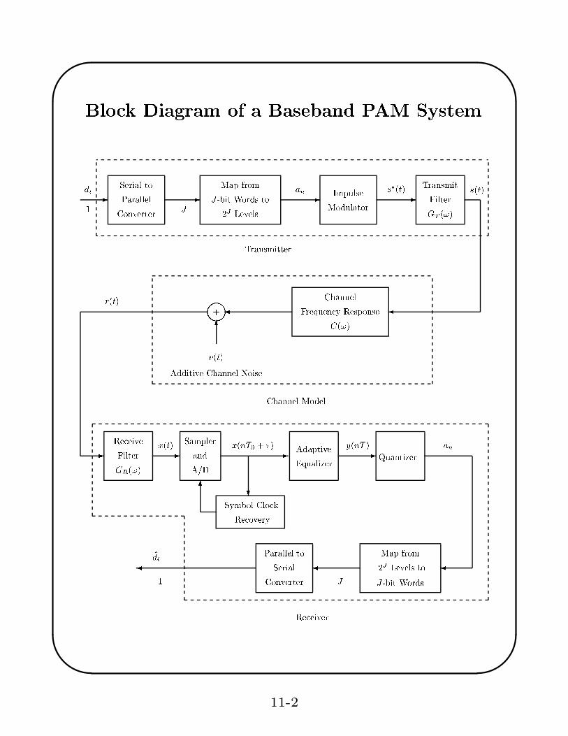
Block Diagram of a Baseband PAM System
Serial to
Parallel
Converter
Map from
J-bit Words to
2
J
Levels
Impulse
Modulator
Sampler
and
A/D
Symbol Clock
Recovery
Adaptive
Equalizer
��
��
- - -
��
6
-
- -
6
?
- -
��
.
.
.
.
.
.
.
.
.
.
.
.
.
.
.
.
.
.
.
.
.
.
.
.
.
.
.
.
.
.
.
.
.
.
.
.
.
.
.
.
.
.
.
.
.
.
.
.
.
.
.
.
.
.
.
.
.
.
.
.
.
.
.
.
.
.
.
.
.
.
.
.
.
.
.
.
.
.
.
.
.
.
.
.
.
.
.
.
.
.
.
.
.
.
.
.
.
.
.
.
.
.
.
.
�
a
n
s
�
(t)
Transmitter
Channel
Frequency Response
C(!)
Additive Channel Noise
Channel Model
Transmit
Filter
r(t)
Map from
Converter
Parallel to
Serial
a
n
1
1
Receiver
^
d
i
v(t)
J
J
J-bit Words
Quantizer
y(nT )x(t) x(nT
0
+ �)
2
J
Levels to
d
i
s(t)
Filter
Receive
+
G
T
(!)
G
R
(!)
11-2

✬
✫
✩
✪
Description of the PAM Block
Diagram
• The transmitter input di is a serial binary
data sequence with a bit rate of Rd bits/sec.
• Input bits are blocked into J-bit words by the
serial-to-parallel converter.
• Input blocks are mapped into the sequence of
symbols an which are selected from an
alphabet of M = 2J distinct voltage levels.
For example, the following levels uniformly
spaced by 2d are commonly used:
ℓi = d(2i− 1) for i = −M
2+ 1, . . . , 0, . . . ,
M
2
The minimum level is −(M − 1)d and the
maximum level is (M − 1)d.
• The symbol rate is fs = 1/T = Rd/J
symbols/sec or baud.
11-3
✬
✫
✩
✪
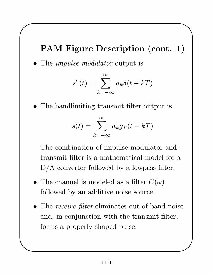
PAM Figure Description (cont. 1)
• The impulse modulator output is
s∗(t) =
∞∑
k=−∞
akδ(t− kT )
• The bandlimiting transmit filter output is
s(t) =∞∑
k=−∞
akgT (t− kT )
The combination of impulse modulator and
transmit filter is a mathematical model for a
D/A converter followed by a lowpass filter.
• The channel is modeled as a filter C(ω)
followed by an additive noise source.
• The receive filter eliminates out-of-band noise
and, in conjunction with the transmit filter,
forms a properly shaped pulse.
11-4

✬
✫
✩
✪
PAM Figure Description (cont. 2)
The combined transmit filter, channel, and
receive filter frequency response is
G(ω) = GT (ω)C(ω)GR(ω)
and the corresponding impulse response is
g(t) = gT (t) ∗ c(t) ∗ gR(t) = F−1{G(ω)}
The combined filter G(ω) is called the
baseband shaping filter.
The output of the receive filter is
x(t) =
∞∑
k=−∞
akg(t− kT ) + v(t) ∗ gR(t)
• The output of the receive filter is sampled at
a rate that is an integer multiple N of the
symbol rate fs. Typically, N might be 3 or 4.
These samples are used by the Symbol Clock
Recovery system to lock the receiver symbol
clock to the transmitter clock.
11-5

✬
✫
✩
✪
PAM Figure Description (cont. 3)
• The Adaptive Equalizer is an FIR filter with
adjustable taps that automatically
compensates for channel amplitude and phase
distortion. It also corrects for small
deviations in the transmit and receive filter
responses from their ideal nominal values. A
least mean-square error (LMS) adaptation
algorithm is used most often.
• The equalizer output is sampled at the
symbol rate and quantized to the nearest
ideal level.
• The Quantizer output is mapped to the
corresponding J-bit binary word and
converted back to a serial output data
sequence.
11-6

✬
✫
✩
✪
Baseband Shaping and Intersymbol
Interference (ISI)
An impulse response with the following property
is said to have no intersymbol interference:
g(nT ) = δ[n] =
1 for n = 0
0 otherwise
Then, if the additive noise is zero, the samples of
the receive filter output at the symbol instants are
x(nT ) =
∞∑
k=−∞
akδ[n− k] = an
which are exactly the transmitted symbols.
The transmit and received filters are usually
designed so their cascade, GT (ω)GR(ω), has no
ISI with, perhaps, some compromise equalization
for the expected channel.
11-7
✬
✫
✩
✪
Eye Diagrams
Normalized Time t/T0 0.2 0.4 0.6 0.8 1 1.2 1.4 1.6 1.8 2
-2
-1.5
-1
-0.5
0
0.5
1
1.5
2
Eye Diagram for a Raised Cosine Channel
with 12% Excess Bandwidth, 2-Level PAM
11-8

✬
✫
✩
✪
Normalized Time t/T0 0.2 0.4 0.6 0.8 1 1.2 1.4 1.6 1.8 2
-5
-4
-3
-2
-1
0
1
2
3
4
5
Eye Diagram for a Raised Cosine Channel
with 12% Excess Bandwidth, 4-Level PAM
With zero noise, baud rate samples of the receive
filter output are
x(nT ) =∞∑
k=−∞
akg(nT − kT )
11-9

✬
✫
✩
✪
x(nT ) = g(0)
an +
∞∑
k=−∞k 6=n
akg(nT − kT )
g(0)
The right-hand sum is the ISI for the received
symbol. The worst case ISI occurs when the
symbols ak have their maximum magnitude
(M − 1)d and the same sign as g(nT − kT ). Then
D = (M − 1)d
∞∑
k=−∞k 6=n
∣
∣
∣
∣
g(nT − kT )
g(0)
∣
∣
∣
∣
= (M − 1)d∞∑
k=−∞k 6=0
∣
∣
∣
∣
g(kT )
g(0)
∣
∣
∣
∣
The peak fractional eye closure is defined to be
η =D
d= (M − 1)
∞∑
k=−∞k 6=0
∣
∣
∣
∣
g(kT )
g(0)
∣
∣
∣
∣
When η is less than 1, the eyes are open.
11-10
✬
✫
✩
✪
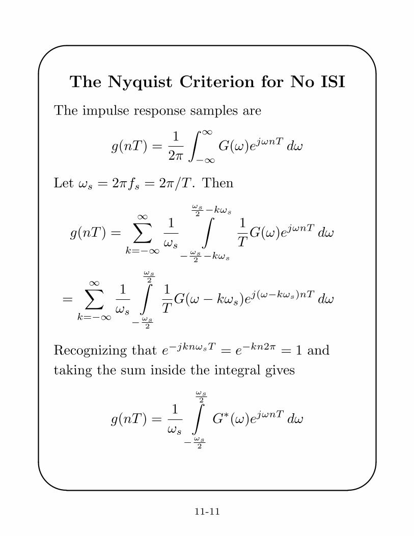
The Nyquist Criterion for No ISI
The impulse response samples are
g(nT ) =1
2π
∫ ∞
−∞
G(ω)ejωnT dω
Let ωs = 2πfs = 2π/T . Then
g(nT ) =
∞∑
k=−∞
1
ωs
ωs
2−kωs∫
−ωs
2−kωs
1
TG(ω)ejωnT dω
=
∞∑
k=−∞
1
ωs
ωs
2∫
−ωs
2
1
TG(ω − kωs)e
j(ω−kωs)nT dω
Recognizing that e−jknωsT = e−kn2π = 1 and
taking the sum inside the integral gives
g(nT ) =1
ωs
ωs
2∫
−ωs
2
G∗(ω)ejωnT dω
11-11

✬
✫
✩
✪
Nyquist’s Criterion (cont.)
where
G∗(ω) =1
T
∞∑
k=−∞
G(ω − kωs)
The function G∗(ω) is called the aliased or folded
spectrum.
There is no ISI if and only if
G∗(ω) = 1
because then the integral at the bottom of the
previous slide becomes
g(nT ) =1
ωs
ωs
2∫
−ωs
2
ejωnT dω = δ[n]
11-12

✬
✫
✩
✪
Raised Cosine Baseband Shaping
Filters
The frequency response of a raised cosine filter is
G(ω) =
T for |ω| ≤ (1− α)ωs
2
T2
{
1− sin[
T2α
(
|ω| − ωs
2
)]}
for (1− α)ωs
2 ≤ |ω| ≤ (1 + α)ωs
2
0 elsewhere
α ∈ [0, 1] is the excess bandwidth factor.
0
0.2
0.4
0.6
0.8
1
0 0.2 0.4 0.6 0.8 1
G(ω)
f/fs
Example for T = 1 and α = 0.5
11-13

✬
✫
✩
✪
Raised Cosine Filters (cont.)
The corresponding impulse response is
g(t) =sin
(
ωs
2 t)
ωs
2 t
cos(
αωs
2 t)
1− 4(αt/T )2
The program C:\DIGFIL\RASCOS.EXE
computes samples of the impulse response
modified by the Hamming window.
Special Cases
• If α = 0, the raised cosine filter becomes an
ideal flat lowpass filter with cutoff frequency
ωs/2.
• If α = 1, the frequency response has no flat
region and is one cycle of a cosine function
raised up so it becomes 0 at the cutoff
frequency of ωs.
• As the bandwidth is increased by making α
closer to 1, the impulse response decays more
rapidly.
11-14

✬
✫
✩
✪
Splitting the Shaping Between the
Transmit and Receive Filters
If the channel amplitude response is flat across
the signal passband and the noise is white, the
amplitude response of the combined baseband
shaping filter should be equally split between the
transmit and receive filters to maximize the
output signal-to-noise ratio, that is,
|GT (ω)| = |GR(ω)| = |G(ω)|1/2
Their phases can be arbitrary as long as the
combined phase is linear.
When raised cosine shaping is used, the transmit
and receive filters are called square-root of raised
cosine filters.
C:\DIGFIL\SQRTRACO.EXE can be used
to compute the impulse response of a square-root
of raised cosine filter.
11-15
✬
✫
✩
✪
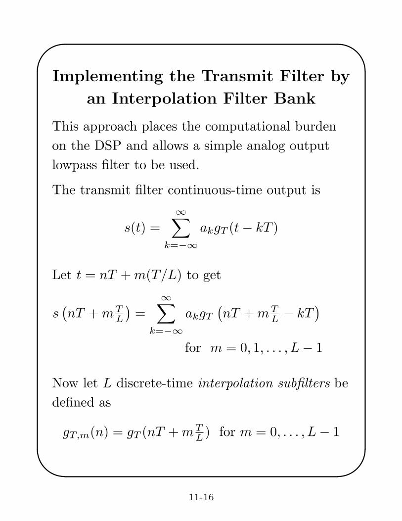
Implementing the Transmit Filter by
an Interpolation Filter Bank
This approach places the computational burden
on the DSP and allows a simple analog output
lowpass filter to be used.
The transmit filter continuous-time output is
s(t) =
∞∑
k=−∞
akgT (t− kT )
Let t = nT +m(T/L) to get
s(
nT +mTL
)
=
∞∑
k=−∞
akgT(
nT +mTL − kT
)
for m = 0, 1, . . . , L− 1
Now let L discrete-time interpolation subfilters be
defined as
gT,m(n) = gT (nT +mTL ) for m = 0, . . . , L− 1
11-16
✬
✫
✩
✪
Interpolation Filters (cont.)
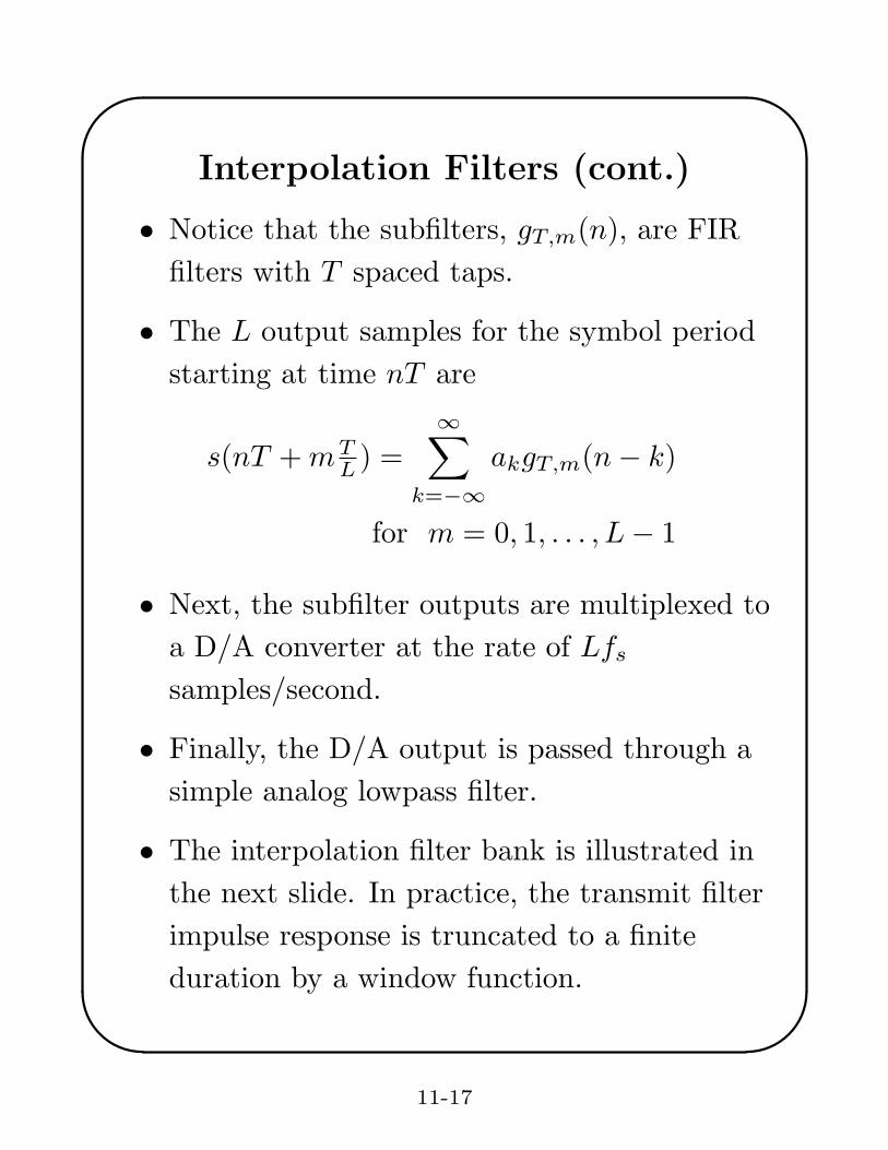
• Notice that the subfilters, gT,m(n), are FIR
filters with T spaced taps.
• The L output samples for the symbol period
starting at time nT are
s(nT +mTL ) =
∞∑
k=−∞
akgT,m(n− k)
for m = 0, 1, . . . , L− 1
• Next, the subfilter outputs are multiplexed to
a D/A converter at the rate of Lfs
samples/second.
• Finally, the D/A output is passed through a
simple analog lowpass filter.
• The interpolation filter bank is illustrated in
the next slide. In practice, the transmit filter
impulse response is truncated to a finite
duration by a window function.
11-17
✬
✫
✩
✪
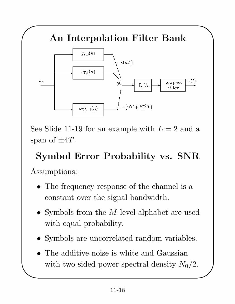
An Interpolation Filter Bank
-
-
-
- - -Q
Q
@
@
B
B
B
B
B
B
B
�
�
�
�
�
�
�
.
.
.
D/A
s(nT )
s
�
nT +
L�1
L
T
�
g
T;0
(n)
g
T;1
(n)
g
T;L�1
(n)
Lowpass
Filter
s(t)a
n
See Slide 11-19 for an example with L = 2 and a
span of ±4T .
Symbol Error Probability vs. SNR
Assumptions:
• The frequency response of the channel is a
constant over the signal bandwidth.
• Symbols from the M level alphabet are used
with equal probability.
• Symbols are uncorrelated random variables.
• The additive noise is white and Gaussian
with two-sided power spectral density N0/2.
11-18

✬
✫
✩
✪
Example of an FIR Filter Bank for L = 2
with Span [−4T, 4T ]
an
TDelay
TDelay
TDelay
TDelay
TDelay
TDelay
TDelay
s(
nT + T
2
)
s(nT )
s(nT ) =7
∑
k=0
g[0][k]an−k
s(
nT + T
2
)
=7
∑
k=0
g[1][k]an−k
Input Symbols
an−1
an−2
g[0][0] g[1][0]
g[0][1] g[1][1]
g[0][2] g[1][2]
an−3
an−4
an−5
an−6
an−7
+ +
g[0][3]
g[0][4]
g[0][5]
g[0][6]
g[0][7]
g[1][3]
g[1][4]
g[1][5]
g[1][6]
g[1][7]
11-19

✬
✫
✩
✪
Symbol Error Probability (2)
• The combined baseband shaping filter has a
raised cosine response with excess bandwidth
factor α and the shaping is split equally
between the transmit and receive filters.
Therefore, the transmit and receive filters
both have square-root of raised cosine
responses.
It can be shown [Lucky, Salz, and Weldon, pp.
52-53] that the average transmitted power is
Ps =E{a2n}
T
1
2π
∫ ∞
−∞
|GT (ω)|2 dω
With the square-root of raised cosine transmit
filter, this reduces to
Ps =E{a2n}
T
11-20

✬
✫
✩
✪
Symbol Error Probability (3)
With equally likely levels, the expected squared
symbol value is
a2 = E{a2n} =2
M
M/2∑
k=1
[d(2k − 1)]2 = (M2 − 1)d2
3
and the transmitted power is
Ps = (M2 − 1)d2
3T(1)
The noise at the output of the square-root of
raised cosine receive filter has the variance
σ2 =1
2π
∫ ∞
−∞
N0
2|GR(ω)|2 dω =
N0
2(2)
Also, the channel noise power in the Nyquist
band (−ωs/2, ωs/2) is
PN =1
2π
∫ ωs/2
−ωs/2
N0
2dω =
N0
2T(3)
11-21

✬
✫
✩
✪
Symbol Error Probability (4)
Since there is no ISI, the samples of the receive
filter output have the form
x(nT ) = an + vR(nT )
where vR(nT ) is a sample of the channel noise
filtered by the receive filter. The received sample
x(nT ) is quantized to the nearest ideal level an.
Error Probability for Inner Points
For the M − 2 inner levels, an error is made if the
noise magnitude exceeds d, half the distance
between points. In this case, the symbol error
probability is
PI = P (|vR(nT )| > d) = 2Q(d/σ)
where Q(x) is the Gaussian tail probability
Q(x) =
∫ ∞
x
1√2π
e−t2
2 dt
11-22

✬
✫
✩
✪
Symbol Error Probability (5)
which is accurately approximated for x > 2 by
Q(x) ≃ 1
x√2π
e−x2
2
Error Probability for the Outer Points
For the level (M − 1)d the error probability is
PO+ = P (vR(nT ) < −d) = Q(d/σ)
For the outer level −(M − 1)d the error
probability is
PO− = P (vR(nT )) > d) = Q(d/σ) = PO+
The total symbol error probability is
Pe =M − 2
MPI +
1
MPO+ +
1
MPO−
= 2M − 1
MQ(d/σ)
11-23

✬
✫
✩
✪
Symbol Error Probability (6)
Solving the transmitted power equation (1) for d
and using formula (2) for the receive filter output
noise power and formula (3) for the channel noise
power, the error probability can be expressed in
terms of the channel signal-to-noise ratio Ps/PN
as
Pe = 2M − 1
MQ
[
(
3
M2 − 1
Ps
PN
)1/2]
Symbol Clock Recovery
The receiver must lock its local symbol clock
frequency and phase to those in the received
signal. A method, good for bandlimited systems,
for deriving the symbol clock from the received
signal is illustrated below.
- -
x(t) Pre�lter
B(!)
q(t)
Squarer- - -
p(t)
q
2
(t)
Bandpass
Filter
H(!)
z(t) �(t)
Phase-
Locked
Loop
System to Generate a Symbol Clock Tone
11-24
✬
✫
✩
✪
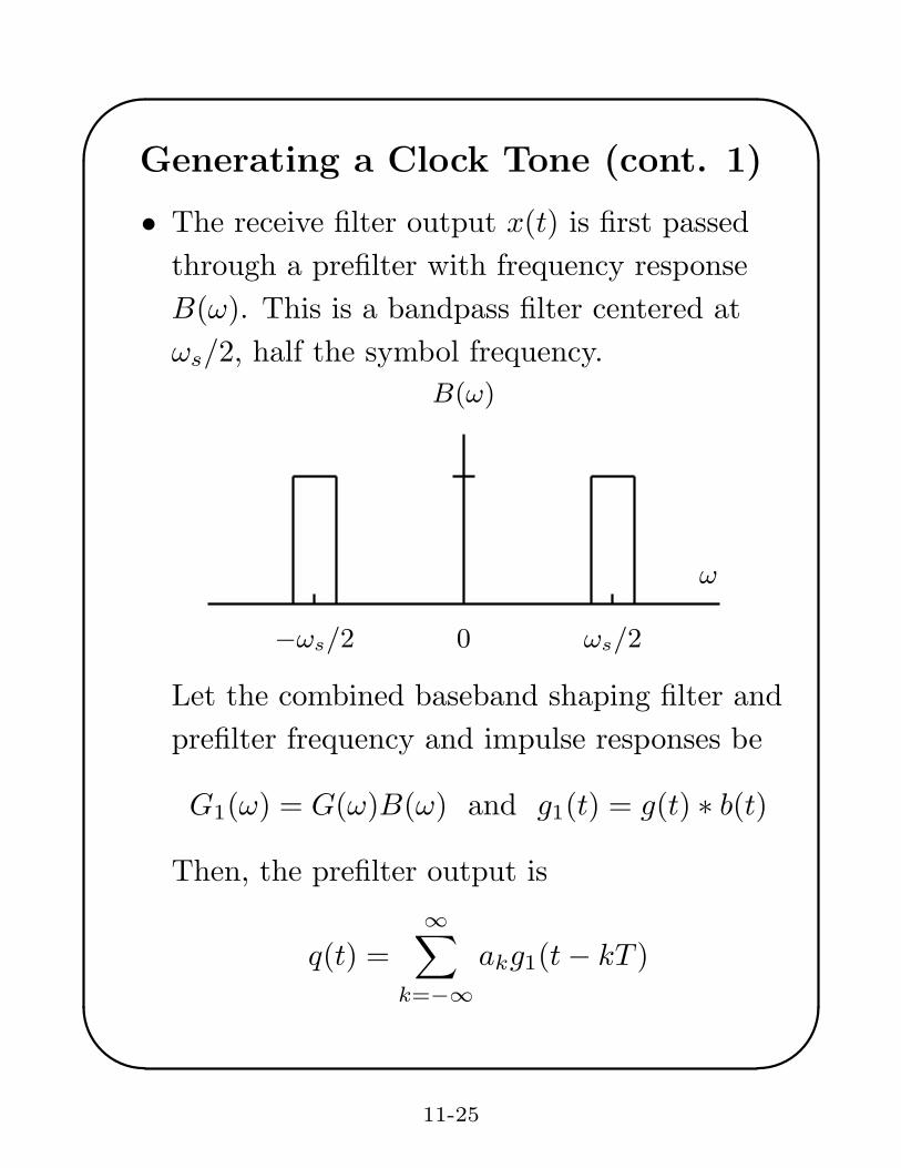
Generating a Clock Tone (cont. 1)
• The receive filter output x(t) is first passed
through a prefilter with frequency response
B(ω). This is a bandpass filter centered at
ωs/2, half the symbol frequency.
B(ω)
−ωs/2 ωs/20
ω
Let the combined baseband shaping filter and
prefilter frequency and impulse responses be
G1(ω) = G(ω)B(ω) and g1(t) = g(t) ∗ b(t)
Then, the prefilter output is
q(t) =
∞∑
k=−∞
akg1(t− kT )
11-25

✬
✫
✩
✪
Generating a Clock Tone (cont. 2)
• The prefilter output is squared to get
p(t) = q2(t)
=
∞∑
k=−∞
∞∑
m=−∞
akamg1(t− kT )g1(t−mT )
• p(t) is passed through a bandpass filter H(ω)
centered at the symbol rate ωs.
0
ω
−ωs ωs
H(ω)
z(t) looks like a sinusoid at the clock
frequency with slowly varying amplitude and
phase. Its zero crossings cluster together. z(t)
is applied to a phase-locked loop to generate
a stable symbol clock.
11-26

✬
✫
✩
✪
Generating a Clock Tone (cont. 3)
It will be assumed that the symbols are a
sequence of zero-mean uncorrelated random
variables. Therefore,
E{akam} = a2δk,m
The expected value of the squarer output is
E{p(t)} =
∞∑
k=−∞
∞∑
m=−∞
E{akam}g1(t− kT )g1(t−mT )
This reduces to
Λ(t) = E{p(t)} = a2∞∑
k=−∞
g21(t− kT )
Λ(t) is periodic with period equal to the symbol
period T . It can be expressed as a Fourier series
of the form
E{p(t)} =
∞∑
k=−∞
pkejkωst
11-27

✬
✫
✩
✪
Generating a Clock Tone (cont. 4)
where
pk =1
T
∫ T
0
E{p(t)}e−jkωst dt
It can be shown that
pk =a2
T
∫ ∞
−∞
g21(t)e−jkωst dt
=a2
T2π
∫ ∞
−∞
G1(ω)G1(kωs − ω) dω
The expected value of the output bandpass filter
is also periodic with the Fourier series expansion
E{z(t)} =
∞∑
k=−∞
zkejkωst
where
zk = pkH(kωs)
= H(kωs)a2
T2π
∫ ∞
−∞
G1(ω)G1(kωs − ω) dω
11-28

✬
✫
✩
✪
Generating a Clock Tone (cont. 5)
• By selecting the prefilter B(ω) to be a narrow
band filter that passes components only near
±ωs/2, it can be seen that pk = 0 except for
k = −1, 0, or 1.
• By selecting the output bandpass filter H(ω)
so that it only passes spectral components
near ±ωs, the k = 0 term is removed and only
the symbol frequency components for k = ±1
remain.
• When the baseband shaping filter has zero
excess bandwidth, that is, when G(ω) = 0 for
|ω| ≥ ωs/2, all the Fourier coefficients pk are
zero for k 6= 0 since the nonzero portions of
G(ω) and G(kωs − ω) do not overlap. This
timing recovery method then fails.
11-29

✬
✫
✩
✪
Generating a Clock Tone (cont. 6)
Condition for Good Timing
Recovery
When G1(ω) is symmetric about ωs/2 and is
bandlimited to the interval
ωs/4 < |ω| < 3ωs/4
and H(ω) is symmetric about ωs, it can be shown
that the variance of z(t) is zero and perfect timing
recovery is possible. When these symmetry
conditions are nearly met, the variations in the
zero crossings of the timing wave z(t) are very
small and the receiver can track the symbol clock
frequency by locking to the zero crossings.
11-30

✬
✫
✩
✪
Theoretical Exercises
1. Write a C function to generate
pseudo-random four-level symbols.
• The function should use a 23-stage self
synchronizing shift register sequence
generator with the connection polynomial
h(D) = 1 +D18 +D23 or 1 +D5 +D23
as discussed in Chapter 9, to generate the
binary sequence dn.
• Generate the four-level sequence an from
pairs of binary symbols (d2n, d2n+1)
according to the rule
an = (−1)d2n(1 + 2d2n+1)d
where d is a desired scale factor.
2. Draw a vertical axis and show the 4 levels.
Label each level with its analog value and
also the corresponding pair of binary digits.
11-31

✬
✫
✩
✪
Theoretical Exercises (cont. 1)
3. Design an interpolation filter bank.
• Use the program
C:\DIGFIL\RASCOS.EXE
to generate the subfilter coefficients.
• Use a symbol rate of fs = 1/T = 4 kHz.
• First, use an excess bandwidth factor of
α = 1.0.
• Truncate the shaping filter impulse
response to the interval [−4T, 4T ] with a
Hamming window.
• Generate L=16 samples of the PAM
signal per symbol interval, that is,
generate the sequence s(kT/16).
4. Generate data for an eye diagram that
extends over two symbol intervals.
• Write enough pairs (mod(k, 32), s(kT/16))
to a file to form a reasonably filled out
4-level eye diagram.
11-32

✬
✫
✩
✪
Theoretical Exercises (cont. 2)
• The function, mod(k, 32), is the remainder
when k is divided by 32 and ranges from 0
to 31. As k increases, mod(k, 32) cycles
throught the values 0, 1, . . . , 31. This
performs the function of resetting the trace
to the left-hand side every two symbols.
• When k reaches a multiple of 32 and
mod(k, 32) = 0, you should write the three
extra points (32, s(kT/16)), (32, 0) and
(0, 0) to the file before writing (0, s(kT/16).
These three points accomplish the
following:
– (32, s(kT/16)) continues the trace to the
right edge of the plot.
– (32, 0) moves the trace vertically to 0.
– (0, 0) moves the trace horizontally at 0
from the right edge back to the origin.
Otherwise, retrace lines will be drawn
11-33

✬
✫
✩
✪
Theoretical Exercises (cont. 3)through the eye diagram for some plotting
programs.
5. Plot the shaping filter impulse response and
eye diagram for α = 1.
6. Change α to 0.125 and generate a new eye
diagram. Plot the new shaping filter impulse
response and eye diagram. Discuss differences
in the impulse responses and eye diagrams for
the two cases.
7. Comment on how the excess bandwidth
factor affects the required symbol sampling
time accuracy in the receiver.
8. Square-Root of Raised Cosine Shaping
Repeat the raised cosine exercises for a
square-root of raised cosine baseband shaping
filter, but only for α = 0.125. Also, compute
the peak fractional eye closure defined on
Slide 11-10 from the shaping filter impulse
response.
11-34

✬
✫
✩
✪
Theoretical Exercises (cont. 4)
9. Theoretical Error ProbabilityThe error probability can be expressed in
terms of the channel signal-to-noise ratio
Ps/PN as
Pe = 2M − 1
MQ
[
(
3
M2 − 1
Ps
PN
)1/2]
under the following conditions:
• A flat channel frequency response.
• Symbols from the M level alphabet are used
with equal probability.
• Symbols selected at different times are
uncorrelated random variables.
• The noise is white and Gaussian with power
spectrum N0/2.
• The transmit and receive filters have
square-root of raised cosine responses.
11-35

✬
✫
✩
✪
Theoretical Exercises (cont. 5)
Plot Pe for M = 2, 4, and 8 on the same graph
as a function of the channel signal-to-noise
ratio Ps/PN . Plot Pe on a logarithmic scale
and 10 log10(Ps/PN ) dB on a linear scale.
10. The power spectral density for a PAM signal
is
S(ω) =E{a2n}
T|GT (ω)|2 (4)
Plot
10 log10
[
S(2πf)/E{a2
n}
T
]
= 20 log10 |GT (2πf)|vs. f for
(a) GT (ω) having a raised cosine shape with
α = 1.
(b) GT (ω) having a raised cosine shape with
α = 0.125.
(c) Repeat the two previous items for the
square-root of raised cosine transmit filter.
11-36
✬
✫
✩
✪
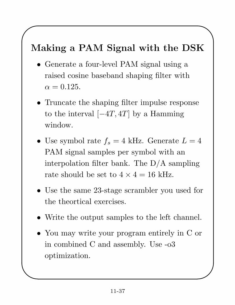
Making a PAM Signal with the DSK
• Generate a four-level PAM signal using a
raised cosine baseband shaping filter with
α = 0.125.
• Truncate the shaping filter impulse response
to the interval [−4T, 4T ] by a Hamming
window.
• Use symbol rate fs = 4 kHz. Generate L = 4
PAM signal samples per symbol with an
interpolation filter bank. The D/A sampling
rate should be set to 4× 4 = 16 kHz.
• Use the same 23-stage scrambler you used for
the theortical exercises.
• Write the output samples to the left channel.
• You may write your program entirely in C or
in combined C and assembly. Use -o3
optimization.
11-37

✬
✫
✩
✪
Frequency Response of the Shaping
Filter
Let the impulse response of the baseband shaping
filter, viewed as an FIR filter with T/4 tap
spacing, be
gn =
g(nT/4) for n = −16,−15, . . . , 16
0 elsewhere
The frequency response of this filter is
G(ω) =
16∑
n=−16
gne−jωnT/4
= g0 + 2
16∑
n=1
gn cos(ωnT/4)
• Compute and plot the amplitude response of
your filter in dB over the frequency range of 0
to 8 kHz. The data for this plot is already
generated by the design program.
11-38
✬
✫
✩
✪
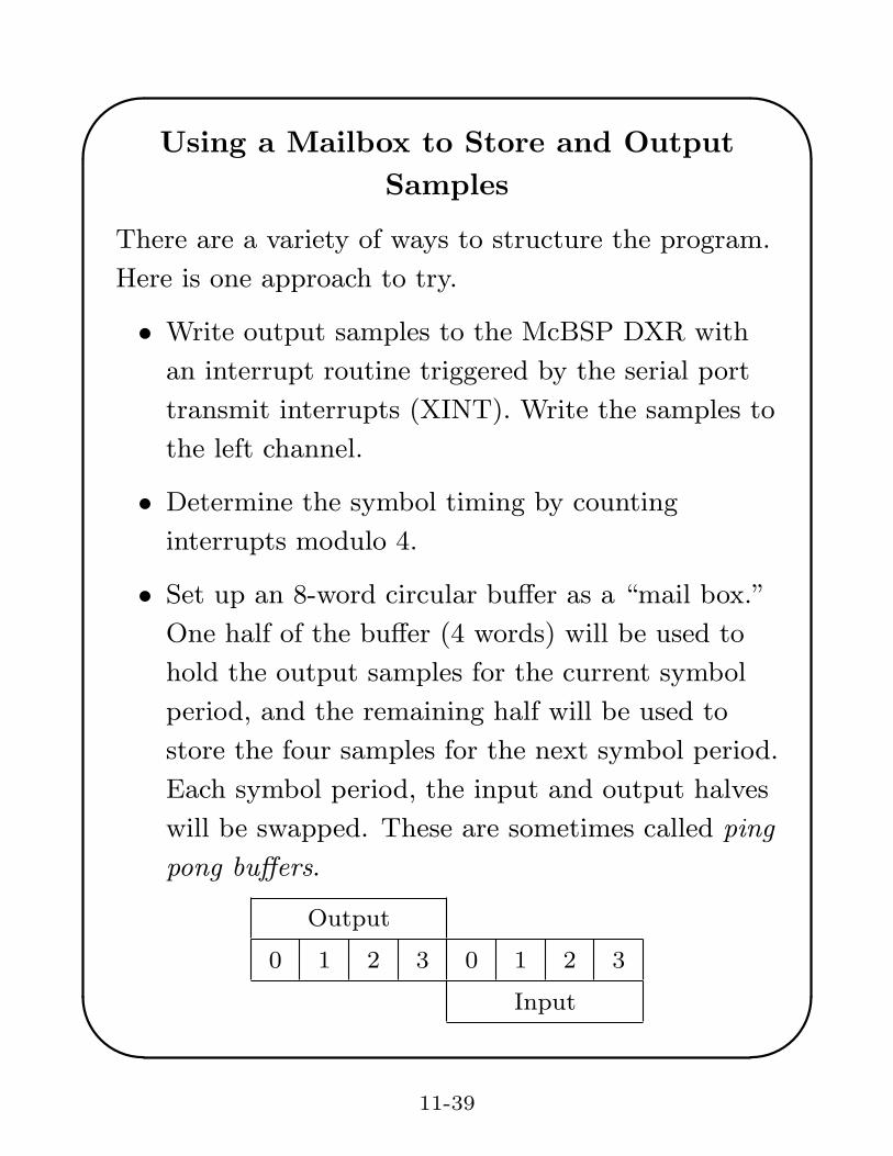
Using a Mailbox to Store and Output
Samples
There are a variety of ways to structure the program.
Here is one approach to try.
• Write output samples to the McBSP DXR with
an interrupt routine triggered by the serial port
transmit interrupts (XINT). Write the samples to
the left channel.
• Determine the symbol timing by counting
interrupts modulo 4.
• Set up an 8-word circular buffer as a “mail box.”
One half of the buffer (4 words) will be used to
hold the output samples for the current symbol
period, and the remaining half will be used to
store the four samples for the next symbol period.
Each symbol period, the input and output halves
will be swapped. These are sometimes called ping
pong buffers.
Output
0 1 2 3 0 1 2 3
Input
11-39

✬
✫
✩
✪
Using a Mailbox (cont.)
• Initialize the output pointer to the address of
the first word in the buffer and the input
pointer to fifth word.
• Before starting data transmission, set the
interrupt count to 0 to indicate the start of a
symbol.
• At the start of each symbol period, generate
four output samples, and write them to the
mailbox. Do this in the main routine.
• The input pointer should be incremented
circularly after each sample is written to the
mailbox.
• After the four samples are written to the
mailbox, the main routine should wait for the
interrupt count to become 0. Remember, the
interrupt routine should count interrupts
modulo 4.
11-40

✬
✫
✩
✪
• The transmit interrupt service routine should
write the sample addressed by the output pointer
to the DXR, increment the output pointer
circularly modulo 8, and increment the interrupt
count modulo 4.
Generating a Baud Synch Signal
• You will need a signal to synchronize the
sweeps with the symbol period to get a
display like your theoretical plot. One way to
generate a synch signal is to create a 4000 Hz
square-wave on the right channel codec
output. You can do this by putting an integer
like A = 16000 in the lower half of the word
sent to the codec for first two samples in a
baud and −A in the second two samples.
Explain why the output does not look like a
square wave.
• Test your program by observing the eye
diagram on the scope. Use DC coupling.
• Measure the transmitted PAM power spectral
density with the oscilloscope and plot it.
11-41

✬
✫
✩
✪
Making a Clock Tone Generator
Write a program for the DSP to implement the
symbol clock recovery system discussed in Slides
11-24 – 11-30 to the point labelled z(t) on Slide
11-24. Do not implement the phase-locked loop.
• Use the same raised cosine baseband shaping
filter you designed for the C6x PAM signal
generator.
• The sampling rate for all operations in the
symbol clock tone generator should be
4fs = 16 kHz.
• Write the PAM output samples to the left
channel D/A converter. Connect the left
channel line output to the left channel line
input. Send the input samples to your clock
tone generation function.
• For the prefilter, B(ω), design a second-order
IIR filter with a center frequency of fs/2 = 2
kHz and roughly a 100 Hz 3 dB bandwidth.
11-42

✬
✫
✩
✪
Making a Tone Generator (cont.)
• For the postfilter, H(ω), design a
second-order bandpass IIR filter with a center
frequency of 4 kHz and a 3 dB bandwidth of
roughly 25 Hz. You should experiment with
these bandwidths and observe how they affect
the system performance.
• Write the tone generator system output
samples z(nT/4) to the right channel output.
Testing the Clock Tone Generator
1. First drive your baseband shaping filter with
the alternating two-level symbol sequence
an = (−1)nd.
• This is called a dotting sequence in the
modem jargon.
• Send the shaping filter output samples to the
left channel output and the clock tone
generator output samples to the right channel
output.
11-43

✬
✫
✩
✪
Testing the Tone Generator
(cont. 1)
Observe the left and right channel outputs
simultaneously on the oscilloscope.
• Notice that an = (−1)n = cos(
ωs
2 nT)
which
are symbol rate samples of a cosine wave that
has a frequency of half the symbol rate.
The sampled signal has spectral components
at the set of frequencies
{ωs/2 + kωs; k = −∞, . . . ,∞}
The shaping filter will pass the 2 kHz
component and heavily attenuate the other
components in the [0, 8) kHz band. In other
words, the PAM signal should be very close
to a 2 kHz sine wave.
11-44

✬
✫
✩
✪
Testing the Tone Generator (cont. 2)
• Check that the tone generator output is a 4
kHz sine wave locked to the PAM signal.
2. Next, use a two-level pseudo-random symbol
sequence having values ±d. Use the shift reg-
ister generator to select the levels. Observe
the PAM signal and clock tone generator out-
put on the oscilloscope. They should still be
locked together. Comment on how the tone
generator output looks compared to the out-
put with the dotting sequence.
3. Finally, use the full four-level pseudo-random
input symbol sequence. Observe the output of
the clock recovery system on the oscilloscope
and compare it with the previous cases.
11-45

✬
✫
✩
✪
Optional Team Exercise
If you are interested in doing more with PAM,
team up with an adjacent group. Make one setup
a PAM transmitter and the other a PAM receiver.
• Transmit a two-level PAM signal. The levels
should be selected by the output of the
23-stage scrambler with an input of 0. Use a
4 kHz symbol rate.
• Sample the received signal at 16 kHz.
• Even though the transmitter and receiver
both use a sampling frequency of 16 kHz,
there will be slight differences due to small
physical and temperature differences in the
oscillator crystals and circuit components.
You will have to devise a method for
synchronizing the symbol clock in the receiver
to the symbol clock in the transmitter.
11-46
✬
✫
✩
✪
Optional Team Exercise (cont. 1)
The sampling phase of the codec cannot be
altered, so you will have to pass the received
samples through a variable phase interpolator
that compensates for the phase difference
between the transmit and receive clocks.
Variable phase interpolators are discussed in
the next chapter. You can lock the phase of
the receiver symbol clock to the positive zero
crossings of the symbol clock tone generator.
In addition you will have to compensate for
any delays in the system so that samples are
taken at the symbol instants, that is, at the
point where the eye has its maximum
opening.
• You should also process the received samples
with a baseband version of the T/2 spaced
adaptive equalizer described in Chapter 15.
The equalizer will automatically adjust for
any symbol sampling phase offset but not for
a frequency offset.
11-47

✬
✫
✩
✪
Optional Team Exercise (cont. 2)
If the received signal has little distortion
(inter-symbol interference), you can add a
filter at the transmitter output or receiver
input to simulate channel distortion. Then
you can observe how the equalizer converges
and opens the eye.
• Quantize the selected symbol rate samples to
a binary sequence. Descramble this sequence
and check that the output is all 0’s.
• Add Gaussian noise to the received samples
in the DSP and make a plot of the bit-error
rate vs. SNR.
11-48