Embed Size (px)
Citation preview
CHAPTER 10
Exercises
E10.1 Solving Equation 10.1 for the saturation current and substituting values, we have
4
15
exp( / ) 110
exp(0.600/0.026) 19.502 10 A
Ds
TD
iIv nV
−
−
=−
=−
= ×
Then for V, we have 0.650Dv =
15exp( / ) 1 9.502 10 exp(0.650/0.026) 1 0.6841 mA
s TD Di I v nV −= − = × × − =
Similarly for V, 0.700Dv = 4.681Di = mA.
E10.2 The approximate form of the Shockley Equation is exp( / )s TD Di I v nV= .
Taking the ratio of currents for two different voltages, we have 1 1
1 22 2
exp( / ) exp ( ) /exp( / )
TD DTD D
TD D
i v nV v v nVi v nV
= = −
Solving for the difference in the voltages, we have: 1 2ln( / )TD Dv nV i i∆ = D
Thus to double the diode current we must increase the voltage by and to increase the current by an order of
magnitude we need ∆ = 0.026ln(2) 18.02 mVDv∆ = =
0.Dv 026ln(10) 59.87 mV=
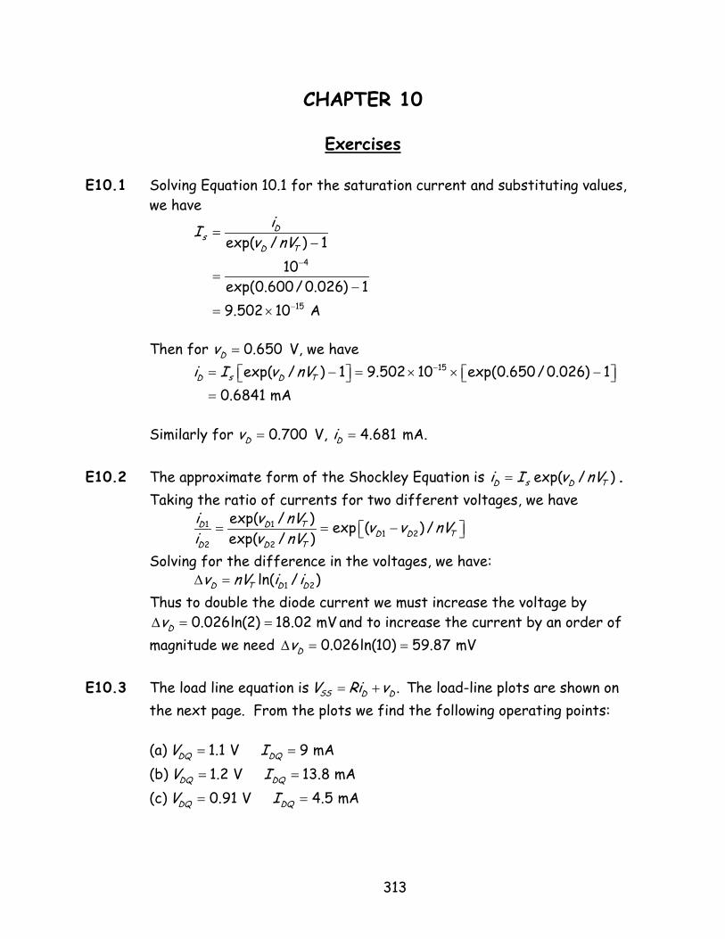
E10.3 The load line equation is .SS D DV Ri v= + The load-line plots are shown on
the next page. From the plots we find the following operating points: (a) 1.1 V 9 mADQ DQV I= = (b) 1.2 V 13.8 mADQ DQV I= = (c) 0.91 V 4.5 mADQ DQV I= =
313
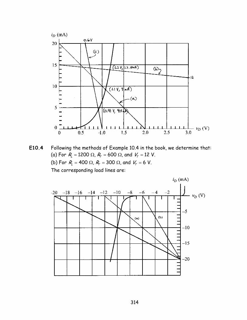
E10.4 Following the methods of Example 10.4 in the book, we determine that: (a) For 1200 , 600 , and 12 V.T TLR R V= Ω = Ω = (b) For 400 , 300 , and 6 V.T TLR R V= Ω = Ω =
The corresponding load lines are:
314

At the intersections of the load lines with the diode characteristic we find (a) ; (b) 9.4 VL Dv v= − ≅ 6.0 VL Dv v= − ≅ .
E10.5 Writing a KVL equation for the loop consisting of the source, the resistor, and the load, we obtain:
15 100( )L Di i v= − − D The corresponding load lines for the three specified values of iL are shown:
At the intersections of the load lines with the diode characteristic, we find (a) (b) 10 V;o Dv v= − = 10 V;o Dv v= − = (c) 5 V.o Dv v= − = Notice that the regulator is effective only for values of load current up to 50 mA.
E10.6 Assuming that D1 and D2 are both off results in this equivalent circuit:
Because the diodes are assumed off, no current flows in any part of the
circuit, and the voltages across the resistors are zero. Writing a KVL equation around the left-hand loop we obtain 1 10Dv = V, which is not consistent with the assumption that D1 is off.
315
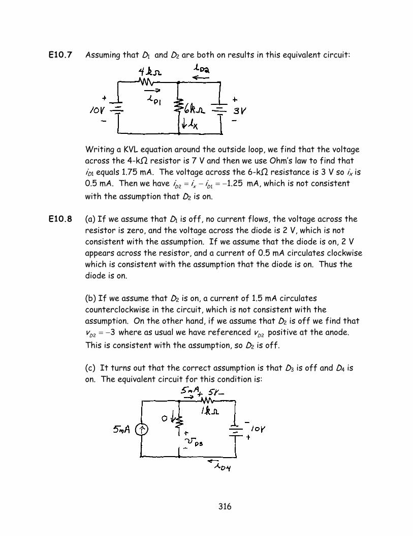
E10.7 Assuming that D1 and D2 are both on results in this equivalent circuit:
Writing a KVL equation around the outside loop, we find that the voltage
across the 4-kΩ resistor is 7 V and then we use Ohm’s law to find that iD1 equals 1.75 mA. The voltage across the 6-kΩ resistance is 3 V so ix is 0.5 mA. Then we have 2 1 1.25xD Di i i= − = − mA, which is not consistent with the assumption that D2 is on.
E10.8 (a) If we assume that D1 is off, no current flows, the voltage across the resistor is zero, and the voltage across the diode is 2 V, which is not consistent with the assumption. If we assume that the diode is on, 2 V appears across the resistor, and a current of 0.5 mA circulates clockwise which is consistent with the assumption that the diode is on. Thus the diode is on. (b) If we assume that D2 is on, a current of 1.5 mA circulates counterclockwise in the circuit, which is not consistent with the assumption. On the other hand, if we assume that D2 is off we find that
where as usual we have referenced positive at the anode. This is consistent with the assumption, so D
2 3Dv = − 2Dv2 is off.
(c) It turns out that the correct assumption is that D3 is off and D4 is on. The equivalent circuit for this condition is:
316

For this circuit we find that 4 5Di = mA and 3 5Dv = − V. These results are consistent with the assumptions.
E10.9 (a) With RL = 10 kΩ, it turns out that the diode is operating on line
segment C of Figure 10.19 in the book. Then the equivalent circuit is:
We can solve this circuit by using the node-voltage technique, treating vo as the node voltage-variable. Notice that .o Dv v= − Writing a KCL equation, we obtain
10 6 02000 12 10000o o ov v v− −
+ + =
Solving, we find V. Furthermore, we find that mA. Since we have
6.017oDv v= − = −
Dv1.39Di = − 6≤ − V and 0,Di ≤ the diode is in fact operating on line segment C.
(b) With RL = 1 kΩ, it turns out that the diode is operating on line
segment B of Figure 10.19 in the book, for which the diode equivalent is an open circuit. Then the equivalent circuit is:
Using the voltage division principle, we determine that V.
Because we have the result is consistent with the assumption that the diode operates on segment B.
3.333Dv = −
6 0,Dv− ≤ ≤
317
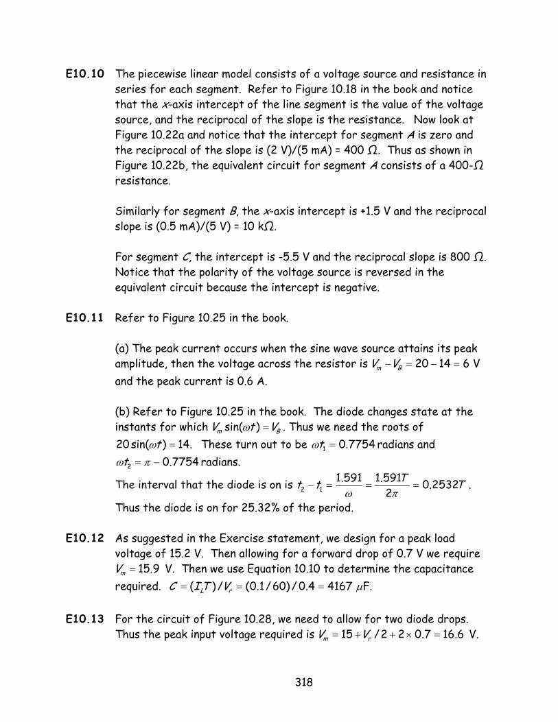
E10.10 The piecewise linear model consists of a voltage source and resistance in series for each segment. Refer to Figure 10.18 in the book and notice that the x-axis intercept of the line segment is the value of the voltage source, and the reciprocal of the slope is the resistance. Now look at Figure 10.22a and notice that the intercept for segment A is zero and the reciprocal of the slope is (2 V)/(5 mA) = 400 Ω. Thus as shown in Figure 10.22b, the equivalent circuit for segment A consists of a 400-Ω resistance. Similarly for segment B, the x-axis intercept is +1.5 V and the reciprocal slope is (0.5 mA)/(5 V) = 10 kΩ. For segment C, the intercept is -5.5 V and the reciprocal slope is 800 Ω. Notice that the polarity of the voltage source is reversed in the equivalent circuit because the intercept is negative.
E10.11 Refer to Figure 10.25 in the book. (a) The peak current occurs when the sine wave source attains its peak amplitude, then the voltage across the resistor is 20 14 6 Vm BV V− = − = and the peak current is 0.6 A. (b) Refer to Figure 10.25 in the book. The diode changes state at the instants for which sin( )m BV t Vω = . Thus we need the roots of 20sin( ) 14.tω = These turn out to be 1 0.7754tω = radians and
2 0.7754tω π= − radians.
The interval that the diode is on is 2 11.591 1.591 0.2532
2Tt t T
ω π− = = = .
Thus the diode is on for 25.32% of the period. E10.12 As suggested in the Exercise statement, we design for a peak load
voltage of 15.2 V. Then allowing for a forward drop of 0.7 V we require 15.9mV = V. Then we use Equation 10.10 to determine the capacitance
required. ( ) / (0.1/60)/0.4 4167 F.rLC I T V µ= = =
E10.13 For the circuit of Figure 10.28, we need to allow for two diode drops. Thus the peak input voltage required is 15 /2 2 0.7 16.6m rV V= + + × = V.
318

Because this is a full-wave rectifier, the capacitance is given by Equation 10.12. ( ) /(2 ) (0.1/60)/0.8 2083 F.rLC I T V µ= = =
1.
−
in.ov v=9.4ov =
3 0.6 1.8 V.× = −
5 <
in.ov v=
52000invi −
=
5 1000 0.ov i= + =
in 52000vi +
=
5 1000o = − +
in( ) 0,v t =
E10.14 Refer to Figure 10.31 in the book.
(a) For this circuit all of the diodes are off if 8 10ov< < . With the diodes off, no current flows and When vin exceeds 10 V, D1 turns on and D2 is in reverse breakdown. Then 0.6 10 V.+ = When vin becomes less than -1.8 V diodes D3, D4, and D5 turn on and
The transfer characteristic is shown in Figure 10.31c.
ov = −
(b) ) For this circuit both diodes are off if 5ov− < . With the diodes off, no current flows and When vin exceeds 5 V, D6 turns on and D7 is in reverse breakdown. Then
a current given by (i is referenced clockwise) flows in the
circuit, and the output voltage is in5 2.5 Vv + When vin is less than -5 V, D7 turns on and D6 is in reverse breakdown.
Then a current given by (still referenced clockwise) flows in
the circuit, and the output voltage is in0.5 2.5 Vv i v= −
E10.15 Answers are shown in Figure 10.32c and d. Other correct answers exist.
E10.16 Refer to Figure 10.34a in the book.
(a) If we have only a dc source in the circuit. In steady state, the capacitor acts as an open circuit. Then we see that D2 is forward conducting and D1 is in reverse breakdown. Allowing 0.6 V for the forward diode voltage the output voltage is -5 V. (b) If the output voltage begins to fall below -5 V, the diodes conduct large amounts of current and change the voltage vC across the capacitor. Once the capacitor voltage is changed so that the output cannot fall
319
below -5 V, the capacitor voltage remains constant. Thus the output voltage is in 2sin( ) 3 V.o Cv v v tω= − = − (c) If the 15-V source is replaced by a short circuit, the diodes do not conduct, vC = 0, and vo = vin.
E10.17 One answer is shown in Figure 10.35. Other correct answers exist. E10.18 One design is shown in Figure 10.36. Other correct answers are possible.
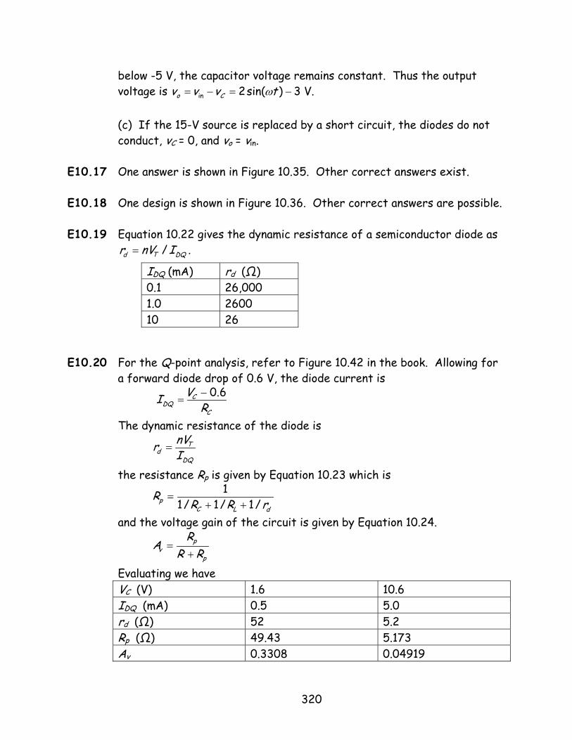
E10.19 Equation 10.22 gives the dynamic resistance of a semiconductor diode as . /T DQdr nV I=
IDQ (mA) rd (Ω) 0.1 26,000 1.0 2600 10 26
E10.20 For the Q-point analysis, refer to Figure 10.42 in the book. Allowing for
a forward diode drop of 0.6 V, the diode current is
0.6CDQ
C
VIR−
=
The dynamic resistance of the diode is
Td
DQ
nVrI
=
the resistance Rp is given by Equation 10.23 which is
11/ 1/ 1/p
C L dR
R R=
+ + r
and the voltage gain of the circuit is given by Equation 10.24.
pv
p
RA
R R=
+
Evaluating we have VC (V) 1.6 10.6 IDQ (mA) 0.5 5.0 rd (Ω) 52 5.2 Rp (Ω) 49.43 5.173 Av 0.3308 0.04919
320
Problems
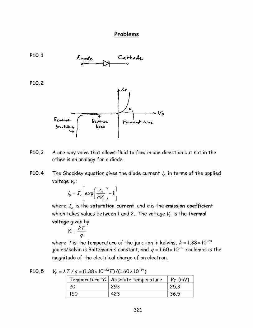
P10.1
P10.2
P10.3 A one-way valve that allows fluid to flow in one direction but not in the
other is an analogy for a diode. P10.4 The Shockley equation gives the diode current in terms of the applied
voltage : Di
Dv
exp 1Ds
T
vnV
= −
Di I
where is the saturation current, and n is the emission coefficient which takes values between 1 and 2. The voltage
sITV is the thermal
voltage given by
TkTVq
=
where T is the temperature of the junction in kelvins, joules/kelvin is Boltzmann's constant, and
231.38 10k −= ×191.60 10q −= × coulombs is the
magnitude of the electrical charge of an electron.
P10.5 )1060.1/()1038.1(/ 1923 −− ××== TqkTVT Temperature °C Absolute temperature VT (mV) 20 293 25.3 150 423 36.5
321
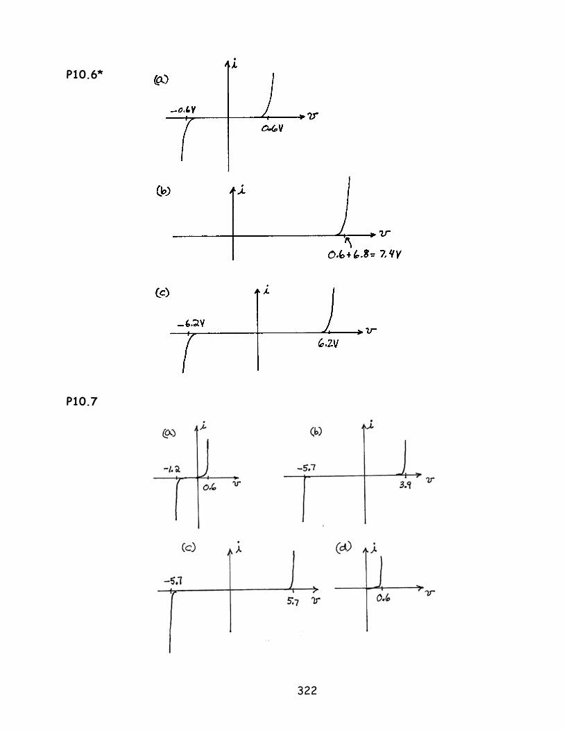
P10.6*
P10.7
322
P10.8* The approximate form of the Shockley Equation is exp( / )s TD Di I v nV= . Taking the ratio of currents for two different voltages, we have
1 11 2
2 2
exp( / ) exp ( ) /exp( / )
TD DTD D
TD D
i v nV v v nVi v nV
= = −
Solving for n we obtain:
336.1)10/1ln(026.0
680.0600.0)/ln( 21
21 =−
=−
=DDT
DD
iiVvvn
Then we have
11
1
1 10150.3)/exp(
−×==TD
Ds nVv
iI A
P10.9 At 175 KT = , we have:
)25175(002.065.0 −−=Dv V 35.0=
P10.10 For Dv 0.6 V, we have =
( )30.2 10 exp 1s TD Di I v n− V = × = −
( )exps TDI v nV≅ Thus, we determine that:
( ) ( )
3-90.2 10 1.950 10 A
exp exp 0.6 (2 0.026D
TD
iv nV
−×=
×sI ≅ = ×
Then, for we have 0.65 V,Dv =
Di I [exp(0.650/0.052) 1] 0.5321 mAs= − =
Similarly, for V, we find 0.700Dv = Di = 1.369 mA.
P10.11 For part (a), Equation 10.3 gives the diode voltage in terms of the current
as ( )ln / 1sTD Dv nV i I = +
For part (b) with a 20-Ω resistance in series, the terminal voltage is v v 100D Di= +
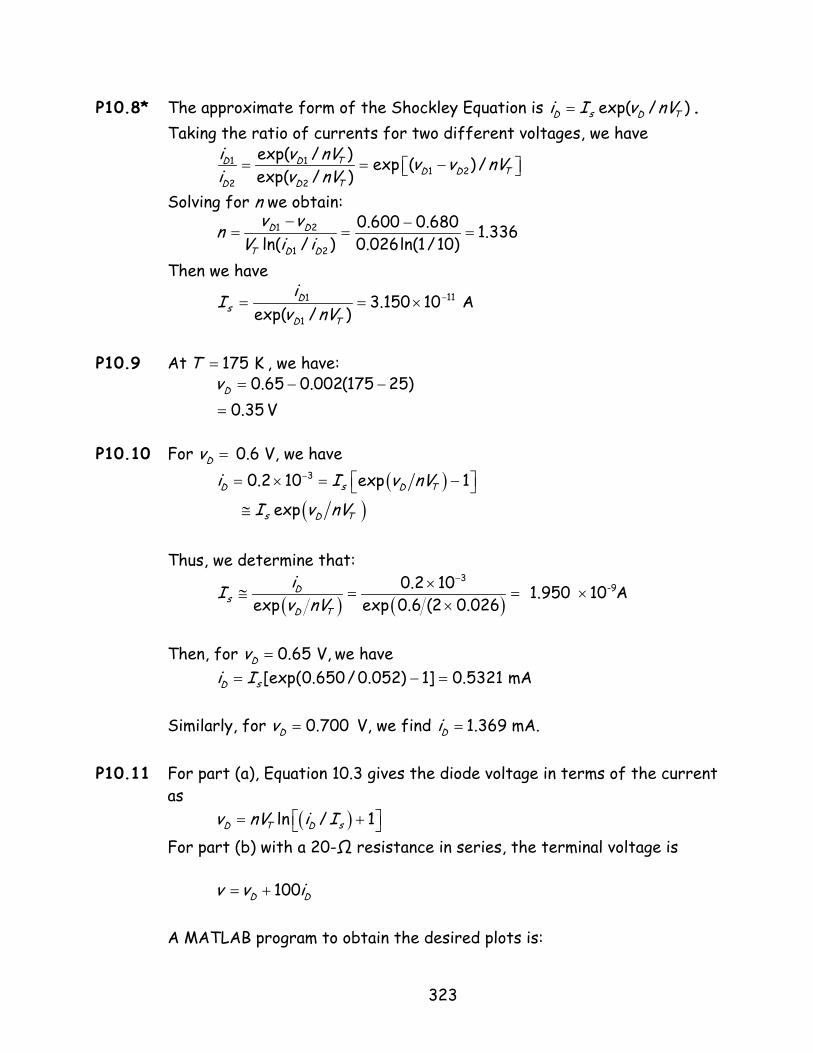
A MATLAB program to obtain the desired plots is:
323
log10_of_id = -5:0.01:-2; id = 10.^log10_of_id; vd = 0.026*log((id/1e-14) + 1); v = vd + 20*id; semilogy(v,id) hold semilogy(vd,id)
(Note in MATLAB log is the natural logarithm.) The resulting plots are shown:
The series resistance is relatively insignificant for currents less than 0.1
mA and is certainly significant for currents greater than 10 mA. P10.12 mV 5.36)1060.1/()4231038.1(/ 1923 =×××== −−qkTVT
5
1
1 10366.3]1)/[exp(
−×=−
=TD
Ds nVv
iI A
mA 016.2]1)/[exp( 22 =−= TDsD nVvIi
324
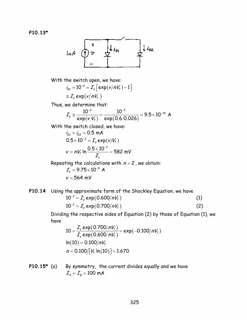
P10.13*
With the switch open, we have: ( )3
1 10 exp 1s Tv nV− = = − Di I
( )exps TI v nV≅ Thus, we determine that:
( ) ( )
3 31410 10 9.5 10 A
exp exp 0.6 0.026sT
Iv V− −
−≅ = = ×
With the switch closed, we have: 1 2 0.5 mAD Di i= =
( )30.5 10 exps TI v V−× =
30.5 10ln 582 mVT
sv nV
I−×
= =
Repeating the calculations with 2n = , we obtain: 99.75 10 AsI −= ×
564 mVv =
P10.14 Using the approximate form of the Shockley Equation, we have (310 exp 0.600s TI− = )nV (1) (210 exp 0.700s TI− = )nV (2) Dividing the respective sides of Equation (2) by those of Equation (1), we have
( )( ) ( )exp 0.700
10 exp 0.100exp 0.600
s TT
s T
I nV nVI nV
= = −
( )ln 10 0.100 TnV= ( )0.100 ln 10 1.67Tn V= = 0
P10.15* (a) By symmetry, the current divides equally and we have
100 mAA BI I= =
325
(b) We have ( )exp 1s TDi I v nV = −
( )exps TI v nV≅ Solving for , we obtain sI
( )exp
Ds
T
iIv nV
=
For diode A, the temperature is 300 KAT = , and we have
23
191.38 10 300 25.88 mV
1.6 10A
TAkTVq
−
−
× ×= = =
×
( )
130.100 1.792 10 Aexp 0.700 0.02588sAI −= = ×
For diode B, we have 305 KT = , and 132 3.583 10sAsBI I −= = × A 26.31 mVTBV = Applying Kirchhoff's current law, we have
0.2 A BI I= +
( ) ( ) ( ) ( )13 130.2 1.792 10 exp 0.02588 3.583 10 exp 0.02631v v− −= × + ×
Solving for v by trial and err, we obtain 697.1 mVv ≅ , , and
. 87 mAAI =
113 mABI =
P10.16* The load-line equation is s s x xV R i v= +
Substituting values, this becomes 3 = + x xi v
Next, we plot the nonlinear device characteristic equation
exp( ) 1 /10x xi v= − and the load line on the same set of axes. Finally, the solution is at the intersection of the load line and the characteristic as shown:
326
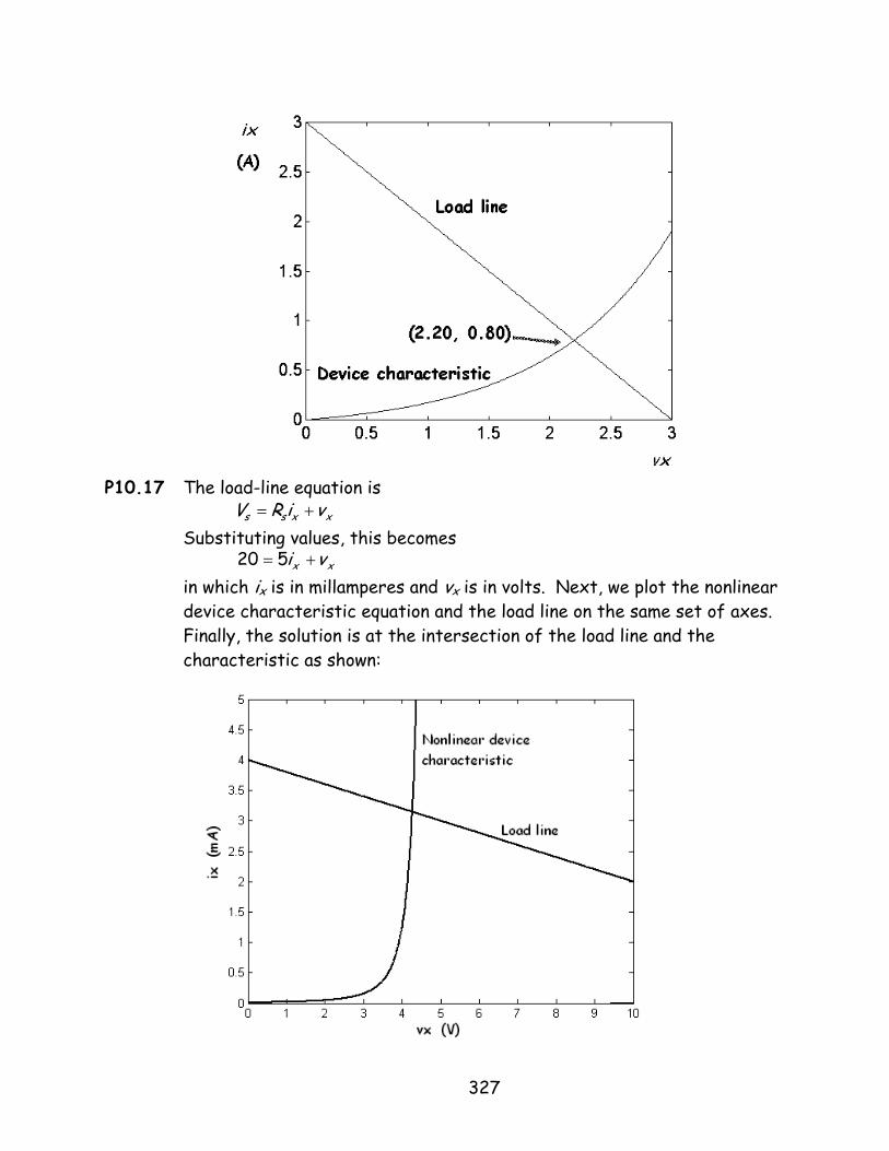
P10.17 The load-line equation is s s x xV R i v= +
Substituting values, this becomes xx vi += 520 in which ix is in millamperes and vx is in volts. Next, we plot the nonlinear device characteristic equation and the load line on the same set of axes. Finally, the solution is at the intersection of the load line and the characteristic as shown:
327
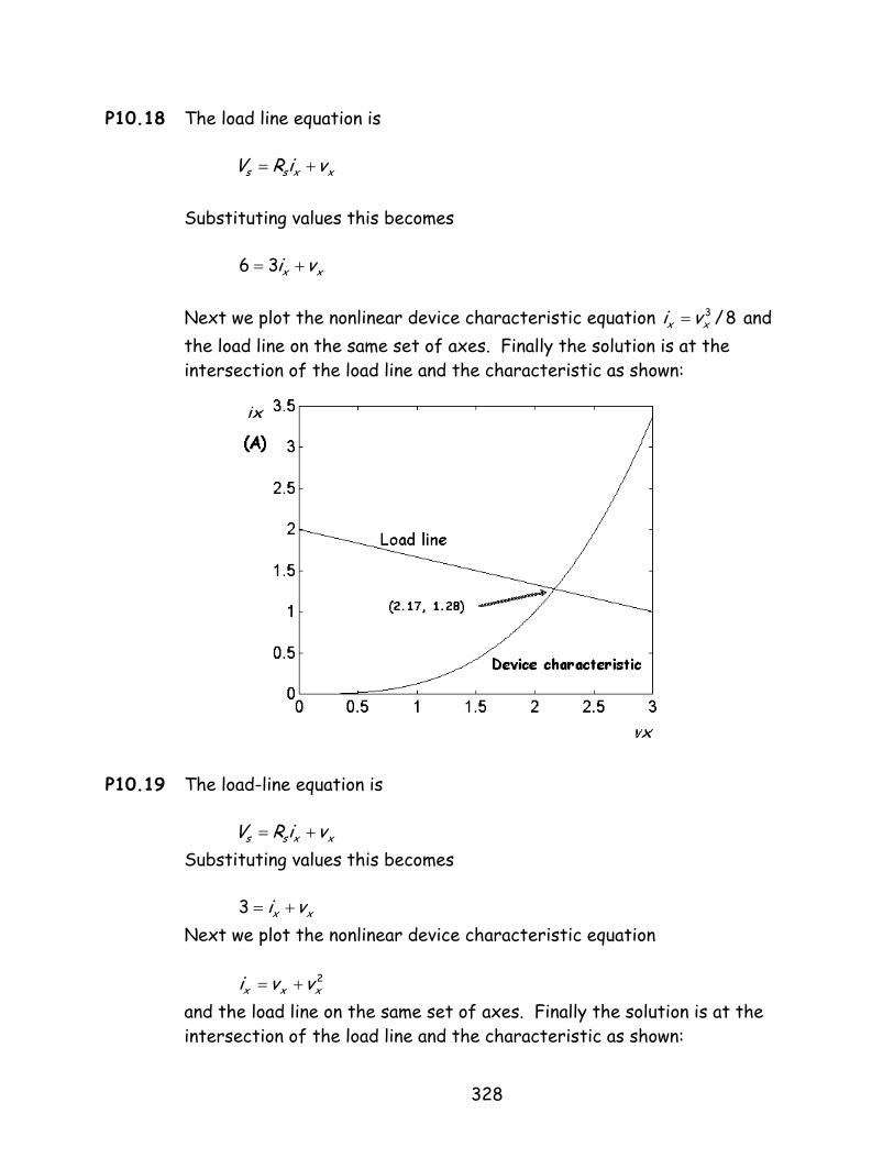
P10.18 The load line equation is s s x xV R i v= +
Substituting values this becomes
6 3 x xi v= +
Next we plot the nonlinear device characteristic equation and the load line on the same set of axes. Finally the solution is at the intersection of the load line and the characteristic as shown:
3 /8x xi v=
P10.19 The load-line equation is
s s x xV R i v= + Substituting values this becomes
3 x xi v= +
Next we plot the nonlinear device characteristic equation
2x xi v v= + x
and the load line on the same set of axes. Finally the solution is at the intersection of the load line and the characteristic as shown:
328
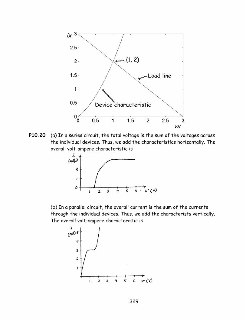
P10.20 (a) In a series circuit, the total voltage is the sum of the voltages across
the individual devices. Thus, we add the characteristics horizontally. The overall volt-ampere characteristic is
(b) In a parallel circuit, the overall current is the sum of the currents through the individual devices. Thus, we add the characterists vertically. The overall volt-ampere characteristic is
329

P10.21 The load-line construction is:
At the intersection of the characteristic and the load line, we have
85.1≅v V and 25.3≅i mA.
P10.22 If we remove the diode, the Thévenin equivalent for the remaining circuit consists of a 12-V source in series with a 3-kΩ resistance. The load line is
At the intersection of the characteristic and the load line, we have the device current 0.31 ≅i mA. Then, applying KCL to the original circuit, we have 0.36 12 =−= ii mA.
330

P10.23 If we remove the diode, the Thévenin equivalent for the remaining circuit consists of a 5-V source in series with a 2-kΩ resistance. The load line is
At the intersection of the characteristic and the load line, we have
70.1≅v V and 7.1≅i mA.
P10.24 If we remove the diode, the Thévenin equivalent for the remaining circuit consists of a 10-V source in series with a 2.5-kΩ resistance. The load line is
At the intersection of the characteristic and the load line, we have
85.1≅v V and 25.3≅i mA.
331

P10.25 A Zener diode is a diode intended for operation in the reverse breakdown region. It is typically used to provide a source of constant voltage. The volt-ampere characteristic of an ideal 5.8-V Zener diode is:
P10.26* The circuit diagram of a simple voltage regulator is:
P10.27 Refer to Figure 10.14 in the book. As the load resistance becomes
smaller, the reverse current through the Zener diode becomes smaller in magnitude. The smallest load resistance for which the load voltage remains at 10 V corresponds to zero diode current. Then, the load current is equal to the current through the 100-Ω resistor given by
50100/)1015( =−=Li mA. Thus, the minimum load resistance is 200/ == LoL ivR Ω.
P10.28 We need to choose Rs so the minimum reverse current through the Zener
diode is zero. Minimum current through the Zener occurs with minimum Vs and maximum iL. Also, we can write:
Ls
LsZ i
RvVi −
−=
Substituting values, we have
1.05100 −−
==s
Z Ri
332
Solving for the resistance we find . 50 Ω=sR Maximum power dissipation in the resistance occurs for maximum Vs.
W 62.1)514()( 22max
max =−
=−
=ss
Ls
RRvVP
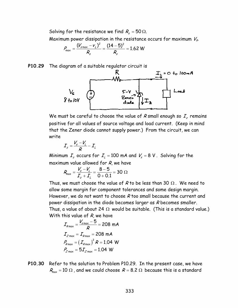
P10.29 The diagram of a suitable regulator circuit is
We must be careful to choose the value of R small enough so remains positive for all values of source voltage and load current. (Keep in mind that the Zener diode cannot supply power.) From the circuit, we can write
zI
s Lz L
V VI IR−
= −
Minimum occurs for zI 100 mA and 8 VsLI V= = . Solving for the maximum value allowed for R, we have
max8 5 30
0 0.1s L
z L
V VRI I
− −= = =
+ +Ω
Thus, we must choose the value of R to be less than 30 Ω . We need to allow some margin for component tolerances and some design margin. However, we do not want to choose R too small because the current and power dissipation in the diode becomes larger as R becomes smaller. Thus, a value of about 24 Ω would be suitable. (This is a standard value.) With this value of R, we have
maxmax
5 208 mAsR
VIR−
= =
max max 208 mAZ RI I= =
( )2max max 1.04 WR RP I R= =
max max5 1.04Z ZP I= = W
Ω
P10.30 Refer to the solution to Problem P10.29. In the present case, we have
, and we could choose max 10 R = 8.2 R = Ω because this is a standard
333
value and we need to provide some design margin. With this value, we have maxmax 610 mAZRI I= =
maxmax 3.05 WZRP P= =
P10.31 Refer to the solution to Problem P10.29. In the present case, we have
, and we would choose max 3.0 R = Ω 2.4 R = Ω because this is a standard value and we need to provide some design margin. With this value, we have maxmax 2.08 AZRI I= =
maxmax 10.4 WZRP P= =
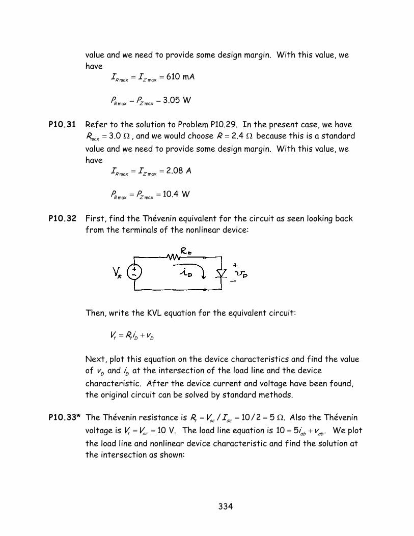
P10.32 First, find the Thévenin equivalent for the circuit as seen looking back
from the terminals of the nonlinear device:
Then, write the KVL equation for the equivalent circuit:
t t D DV R i v= + Next, plot this equation on the device characteristics and find the value of at the intersection of the load line and the device characteristic. After the device current and voltage have been found, the original circuit can be solved by standard methods.
and Dv Di
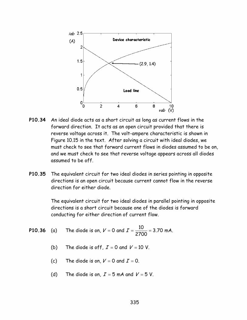
P10.33* The Thévenin resistance is / 10/2 5 .t oc scR V I= = = Ω Also the Thévenin
voltage is 10 V.t ocV V= = The load line equation is 10 5 .ab abi v= + We plot the load line and nonlinear device characteristic and find the solution at the intersection as shown:
334
P10.34 An ideal diode acts as a short circuit as long as current flows in the
forward direction. It acts as an open circuit provided that there is reverse voltage across it. The volt-ampere characteristic is shown in Figure 10.15 in the text. After solving a circuit with ideal diodes, we must check to see that forward current flows in diodes assumed to be on, and we must check to see that reverse voltage appears across all diodes assumed to be off.
P10.35 The equivalent circuit for two ideal diodes in series pointing in opposite directions is an open circuit because current cannot flow in the reverse direction for either diode.
The equivalent circuit for two ideal diodes in parallel pointing in opposite
directions is a short circuit because one of the diodes is forward conducting for either direction of current flow.
P10.36 (a) The diode is on, 100 and 3.70 mA.2700
V I= = =
(b) The diode is off, 0 and 10 V.I V= = (c) The diode is on, 0 and 0.V I= = (d) The diode is on, 5 mA and 5 V.I V= =
335
P10.37* (a) 1 2 is on and is off. 10 volts and 0.D D V I= = (b) 1 2 is on and is off. 6 volts and 6 mA.D D V I= = (c) 1 2Both and are on. 30 volts and 33.6 mA.D D V I= =
P10.38 (a) D D1 2 3 is on, is on, and is off. 7.5 volts and 0.D V I= = (b) inV 1D 2D 3D 4D V I 0 on on on on 0 0 2 on on on on 2 V 2 mA 6 off on on off 5 V 5 mA 10 off on on off 5 V 5 mA The plot of V versus Vin is:
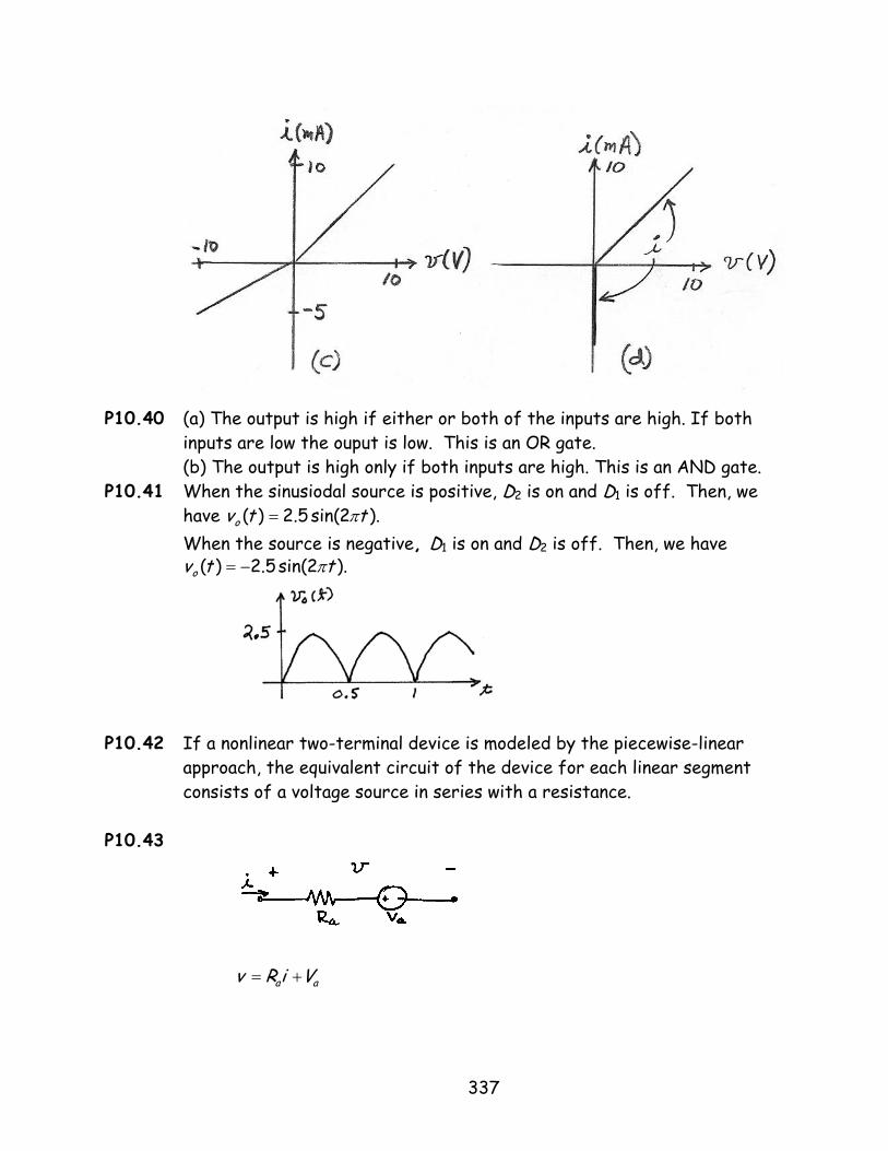
P10.39
336
P10.40 (a) The output is high if either or both of the inputs are high. If both
inputs are low the ouput is low. This is an OR gate. (b) The output is high only if both inputs are high. This is an AND gate.
P10.41 When the sinusiodal source is positive, D2 is on and D1 is off. Then, we have ).2sin(5.2)( ttvo π= When the source is negative, D1 is on and D2 is off. Then, we have
).2sin(5.2)( ttvo π−=
P10.42 If a nonlinear two-terminal device is modeled by the piecewise-linear
approach, the equivalent circuit of the device for each linear segment consists of a voltage source in series with a resistance.
P10.43
a av R i V= +
337
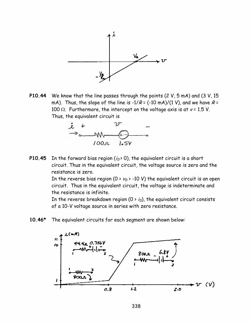
P10.44 We know that the line passes through the points (2 V, 5 mA) and (3 V, 15
mA). Thus, the slope of the line is -1/R = (-10 mA)/(1 V), and we have R = 100 Ω. Furthermore, the intercept on the voltage axis is at v = 1.5 V. Thus, the equivalent circuit is
P10.45 In the forward bias region (iD > 0), the equivalent circuit is a short
circuit. Thus in the equivalent circuit, the voltage source is zero and the resistance is zero.
In the reverse bias region (0 > vD > -10 V) the equivalent circuit is an open circuit. Thus in the equivalent circuit, the voltage is indeterminate and the resistance is infinite.
In the reverse breakdown region (0 > iD), the equivalent circuit consists of a 10-V voltage source in series with zero resistance.
10.46* The equivalent circuits for each segment are shown below:
338

For the circuit of Figure P10.46a, we can determine by trial and err (or by a load-line analysis) that the device operates on the middle line segment. Thus, the equivalent circuit is:
15 0.756 4.68 mA
3000 44.4−+
i = =
v i 0.756 44.4 0.964 V= + = For the circuit of Figure P10.46b, we can determine by trail and err that
the device operates on the upper right-hand line segment. Thus, the equivalent circuit is:
mA 4.10
800508.62
=++
=i
= V 48.18.6800 =−iv
P10.47* For small values of iL, the Zener diode is operating on line segment C of Figure 10.19, and the equivalent circuit is
339
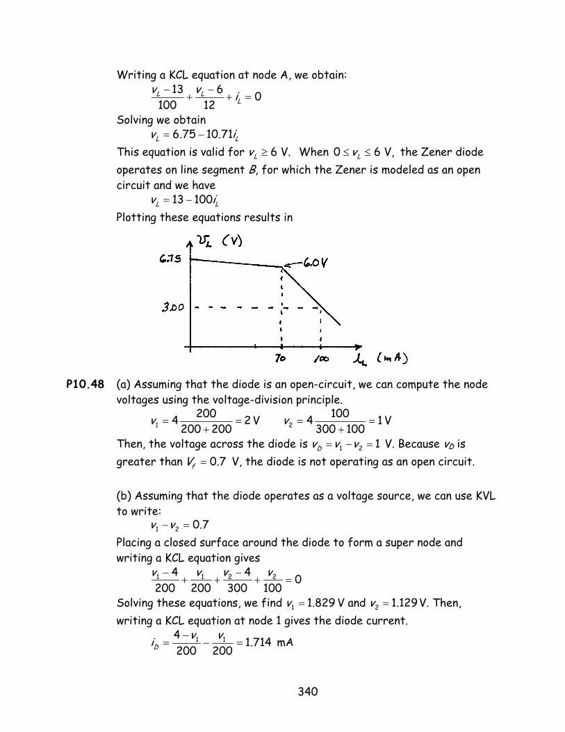
Writing a KCL equation at node A, we obtain:
13 6 0100 12L L
Li− −
+ + =v v
Solving we obtain v i 6.75 10.71L L= −
This equation is valid for When 06 V.Lv ≥ 6 V,Lv≤ ≤ the Zener diode operates on line segment B, for which the Zener is modeled as an open circuit and we have
v i 13 100L L= −
Plotting these equations results in
P10.48 (a) Assuming that the diode is an open-circuit, we can compute the node
voltages using the voltage-division principle.
V 2200200
20041 =+
=v V 1100300
10042 =+
=v
Then, the voltage across the diode is 121 =−= vvvD V. Because vD is greater than 7.0=fV V, the diode is not operating as an open circuit. (b) Assuming that the diode operates as a voltage source, we can use KVL to write: 7.021 =−vv Placing a closed surface around the diode to form a super node and writing a KCL equation gives
0100300
4200200
4 2211 =+−
++− vvvv
Solving these equations, we find 829.11 =v V and 129.12 =v V. Then, writing a KCL equation at node 1 gives the diode current.
714.1200200
4 11 =−−
=vviD mA
340

Because the diode current is positive, the diode operation is consistent with the model.
P10.49 Half-wave rectifier with a capacitance to smooth the output voltage:
Full-wave circuits:
P10.50 The peak value of the ac source is 28.28220 ==mV V. Thus the PIV is
28.28 V and the peak current is 282.8 mA. P10.51 The diode is on for )sin( tVV mB ω≤ . Substituting values and solving, we
find that during the first cycle after t = 0 the diode is on for 6/5)24/12arcsin(6/)24/12arcsin( π=−π≤ω≤π= t
The current is given by
6)sin(122
12)sin(24( −ω=−ω
= t) tti A
The charge passing through the circuit during the first cycle is
ωπ−
=
−ω
ω−=−ω=
ωπ
ωπ
ωπ
ωπ∫
43126)cos(12]6)sin(12[6/5
6/
6/5
6/1 ttdttQ
The average current is the charge passing through the circuit in 1 second (or 60 cycles). Also, we have π=ω 120 Thus
308.1236120
431260431260 =−=−
=−
=ππ
πω
πavgI A
Then the time required to fully charge the battery is
45.76308.1100
==T hours
341
P10.52 The dc output voltage is equal to the peak value of the ac source, which is 28.28220 ==Lv V. The load current is 8.282/ == LLL Rvi mA. The
charge that passes through the load must also pass through the diode. The charge is 714.460/2828.0 === TiQ L mC. The peak inverse voltage is 56.57 V.
P10.53 (a) The integral of )sin( tVm ω over one cycle is zero, so the dc voltmeter reads zero.
(b) π
=
ω
ω−=
+ω=
=
=∫∫ m
Tt
t
mT
T
T
mavgVtV
TdtdttV
TV
2/
02/
2/
0
)cos(10)sin(1
(c) π
=
ω−+ω= ∫∫ m
T
Tm
T
mavgVdttVdttV
TV 2)sin()sin(1
2/
2/
0
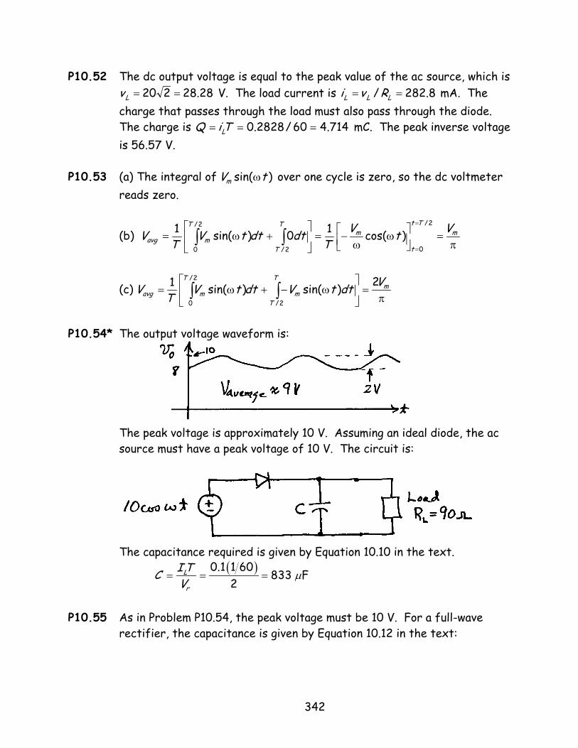
P10.54* The output voltage waveform is:
The peak voltage is approximately 10 V. Assuming an ideal diode, the ac source must have a peak voltage of 10 V. The circuit is:
The capacitance required is given by Equation 10.10 in the text.
( )0.1 1 60833 F
2L
r
I TCV
µ= = =
P10.55 As in Problem P10.54, the peak voltage must be 10 V. For a full-wave
rectifier, the capacitance is given by Equation 10.12 in the text:
342
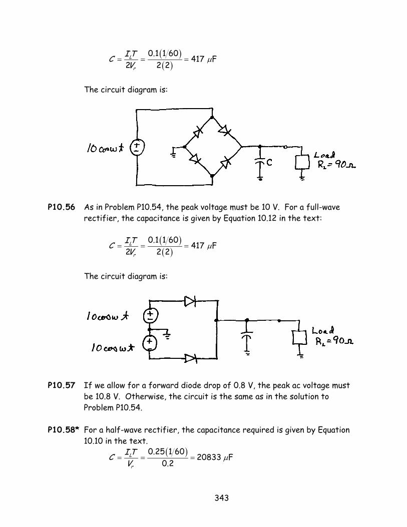
( )( )
0.1 1 60417 F
2 2 2L
r
I TCV
µ= = =
The circuit diagram is:
P10.56 As in Problem P10.54, the peak voltage must be 10 V. For a full-wave
rectifier, the capacitance is given by Equation 10.12 in the text:
( )( )
0.1 1 60417 F
2 2 2L
r
I TCV
µ= = =
The circuit diagram is:
P10.57 If we allow for a forward diode drop of 0.8 V, the peak ac voltage must be 10.8 V. Otherwise, the circuit is the same as in the solution to Problem P10.54.
P10.58* For a half-wave rectifier, the capacitance required is given by Equation 10.10 in the text.
( )0.25 1 6020833 F
0.2L
r
I TV
C µ= = =
343

For a full-wave rectifier, the capacitance is given by Equation 10.12 in the text:
( )( )
0.25 1 6010416 F
2 2 0.2L
r
I TCV
µ= = =
P10.59 (a) The current pulse starts and ends at the times for which v t ( )s BV= 20sin(200 ) 12tπ =
Solving we find that 1
startsin (0.6) 1.024 ms
200t
π
−
= = and startend 3.976 ms2
Tt t= − =
Between these two times the current is
20sin(200 ) 12( )80
ti t π −=
A sketch of the current to scale versus time is
(b) The charge flowing through the battery in one period is
20 sin(200 ) 12( )80
1 12cos(200 ) 800 80
end end
start start
end
start
t t
t tt
t
tQ i t dt dt
tt
π
ππ
−= =
= − −
∫ ∫
194 CQ µ= Finally, the average current is the charge divided by the period.
6
3194 10 19.4 mA10 10avg
QIT
−
−
×= = =
×
P10.60 (a) With ideal diodes and a large smoothing capacitance, the load voltage
equals the peak source voltage which is Vm = 12 V. Then the PIV is 2Vm = 24 V.
344
(b) Here again with ideal diodes and a large smoothing capacitance, the load voltage equals the peak source voltage which is Vm = 12 V. However the PIV is only Vm = 12 V.
P10.61 (a) The circuit operates as three full-wave rectifiers with a common load
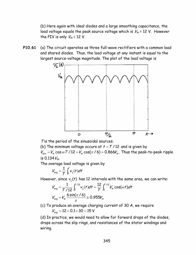
and shared diodes. Thus, the load voltage at any instant is equal to the largest source-voltage magnitude. The plot of the load voltage is
T is the period of the sinusoidal sources. (b) The minimum voltage occurs at 12/Tt = and is given by
mmm VVTVV 866.0)6/cos(12/cosmin === πω . Thus the peak-to-peak ripple is 0.134Vm.
The average load voltage is given by
( )∫=T
L dttvT
V0avg
1
However, since )(tvL has 12 intervals with the same area, we can write:
( ) ∫∫ ==12/
0
12/
0avg )cos(1212/
1 Tm
TL dttV
Tdttv
TV ω
mm VVV 955.0)6/sin(6avg ≅=
ππ
(c) To produce an average charging current of 30 A, we require 15301.012 =×+=avgV V (d) In practice, we would need to allow for forward drops of the diodes, drops across the slip rings, and resistances of the stator windings and wiring.
345

P10.62 A clipper circuit removes or clips part of the input waveform. An example circuit with waveforms is:
We have assumed a forward drop of 0.6V for the diode.
P10.63 Refer to Figure P10.63 in the book. When the source voltage is negative, diode D3 is on and the output vo(t) is zero. For source voltages between 0 and 10 V, none of the diodes conducts and vo(t) = vs(t). Finally when the source voltage exceeds 10 V, D1 is on and D2 is in the breakdown region so the output voltage is 10 V. The waveform is:
346
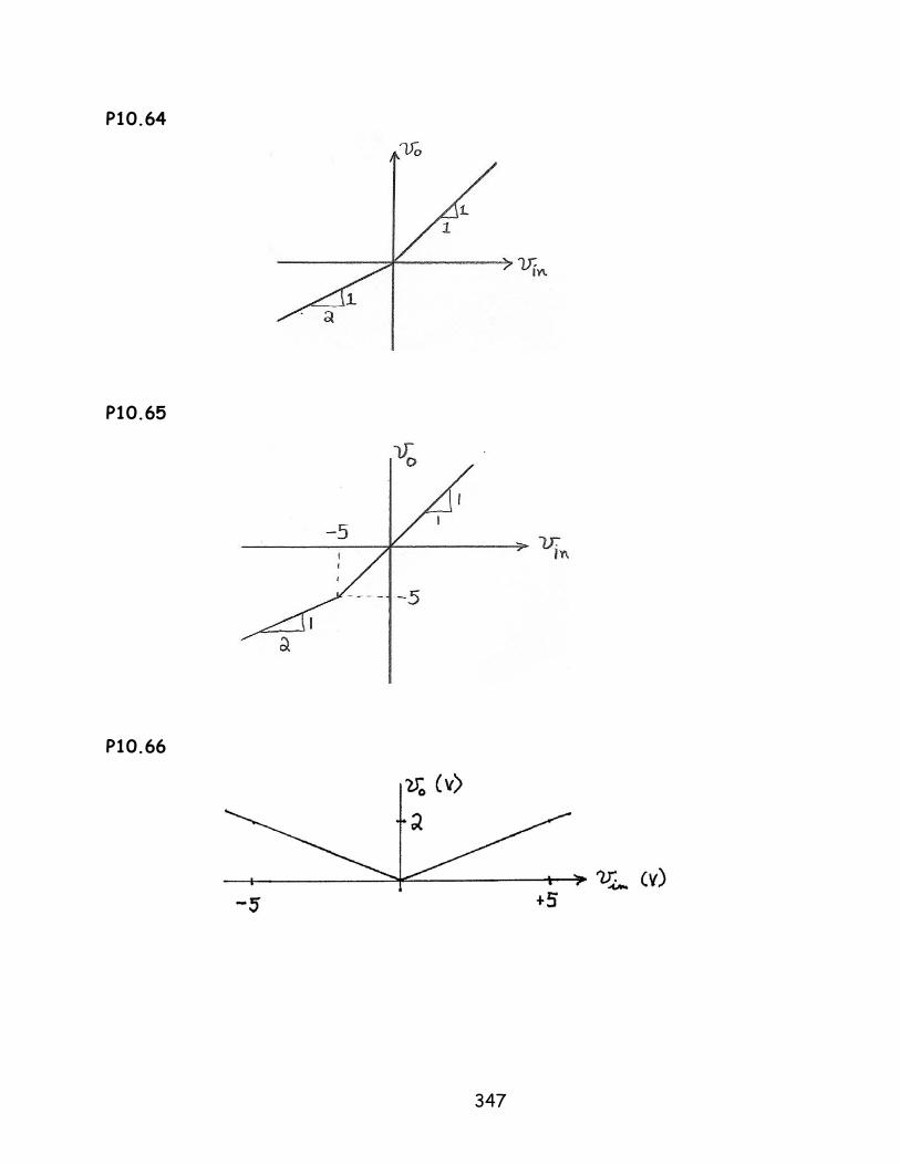
P10.64
P10.65
P10.66
347

P10.67
P10.68 A clamp circuit adds or subtracts a dc component to the input waveform
such that either the positive peak or the negative peak is forced to assume a predetermined value. An example circuit that clamps the positive peak to +5 V is shown below:
We have allowed a forward drop of 0.6 V for the diode.
P10.69 This is a clamp circuit that clamps the positive peaks to zero.
348

P10.70* Refer to the circuit shown in Figure P10.70 in the book. If the output
voltage attempts to become less than -5 V, the Zener diode breaks down and current flows, charging the capacitance. Thus the negative peak is clamped to -5 V. The input and output waveforms are:
P10.71
The capacitor and diode act as a clamp circuit that clamps the negative peak of to zero. Thus, the waveform at point A is:
1C 1D( )Av t
349

Diode and capacitor act as a half-wave peak rectifier. Thus, the voltage across is the peak value of
2D 2C
LR ( )Av t . Thus, ( ) 2 mLv t V≅
mV
. This is called a voltage-doubler circuit because the load voltage is twice the peak value of the ac input. The peak inverse voltage is 2 for both diodes.
P10.72* A suitable circuit is:
P10.73 A suitable circuit is:
350
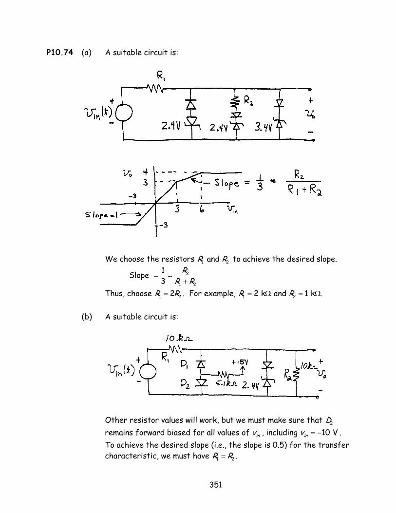
P10.74 (a) A suitable circuit is:
We choose the resistors to achieve the desired slope. 1 and R 2R
2
1 2
1ope 3
RR R
= =Sl+
Thus, choose 1 2R 2R= . For example, 1 22 k and 1 k .R R= Ω = Ω
(b) A suitable circuit is:
Other resistor values will work, but we must make sure that remains forward biased for all values of , including . To achieve the desired slope (i.e., the slope is 0.5) for the transfer characteristic, we must have
2D10 Vinv inv = −
1 2R R= .
351
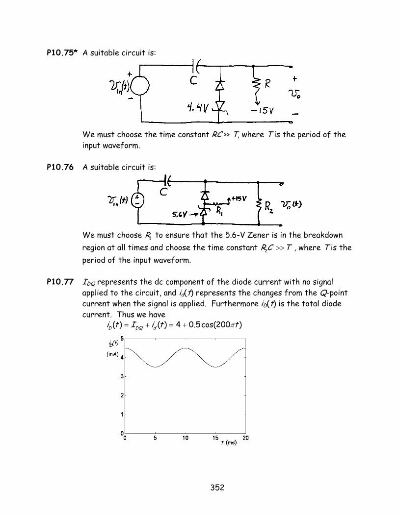
P10.75* A suitable circuit is:
We must choose the time constant RC >> T, where T is the period of the input waveform.
P10.76 A suitable circuit is:
We must choose to ensure that the 5.6-V Zener is in the breakdown region at all times and choose the time constant , where T is the period of the input waveform.
1R
2R C T>>
P10.77 IDQ represents the dc component of the diode current with no signal
applied to the circuit, and id(t) represents the changes from the Q-point current when the signal is applied. Furthermore iD(t) is the total diode current. Thus we have
i t( ) ( ) 4 0.5cos(200 )D DQ dI i t tπ= + = +
352

P10.78 The small signal equivalent circuit of a diode is a resistance known as the dynamic resistance. The dynamic resistance is the reciprocal of the slope of the characteristic at the operating point. versus Di Dv
P10.79 Dc sources voltage sources are replaced by short circuits in a small-signal
equivalent circuit. By definition the voltage across a dc voltage source is constant. Thus, even if there is ac current flowing through the dc source the ac voltage across it is zero as is the case for a short circuit.
P10.80 We should replace dc current sources by open circuits in a small-signal equivalent circuit. The current through a dc current source is constant. Thus, the ac current must be zero even if we apply an ac voltage. Zero current for a non-zero applied voltage implies that we have an open circuit.
P10.81* A plot of the device characteristic is:
Clearly this device is not a diode because it conducts current in both directions. The dynamic resistance is given by:
1
28
3D
D D
didv v
−
Dr = =
A plot of the dynamic resistance versus vD is:
353

P10.82 We are given
( )
6
310 for 5 V 0
1 5D DD
i vv
−−= − <
+<
A plot of this is:
The dynamic resistance is:
1 4
61.67 10 15
D DD
D
di vrdv
− = = × × +
To find the dynamic resistance at a given Q-point, we evaluate this expression for . D Dv V= Q
rr
For 1.0 mA, we have 4.5 V and 167 .DQ DQ DI V= − = − = Ω
For 10.0 mA, we have 4.77 V and 7.48 .DQ DQ DI V= − = − = Ω
354

P10.83 We are given vD(t) = 5 + 0 .01cos(ωt) V and iD(t) = 3 + 0.2cos(ωt) mA. The dynamic resistance is the ratio of the ac voltage amplitude to the ac current amplitude.
Ω=×
= − 50102.001.0
3d
d
i=D
vr
The Q-point results if we set the ac signals to zero. Thus, we have DQ V 5=V and mA 3=DQI P10.84 Dynamic resistance is given by
1
D D
D D
di dvdv di
−
Dr = =
Because voltage is constant for changes in current, the dynamic resistance is zero for an ideal Zener diode in the breakdown region.
P10.85* To find the Q-point, we ignore the ac ripple voltage and the circuit
becomes:
Thus, we have:
8 5 150 mA20−
= =sQI
5 100 50 mALQI = = 100 mAsQDQ LQI I I= − = The small-signal or ac equivalent circuit is:
where is the dynamic resistance of the Zener diode. Using the voltage-division principle, the ripple voltage across the load is
Dr
pLac ripple
p
Rv V
R R= ×
+
355
where 11 1p
L DR
R r=
+ is the parallel combination of the load resistance
and the dynamic resistance of the diode. Substituting values, we find
310 10 120
pLac
p
RV
R−= × = ×
+
Solving, we find . Then, we have: 0.202 pR = Ω
10.2021 100 1p
DR
r= =
+ which yields 0.202 Dr = Ω .
356


![SIGNATURE SERIES Operational Amplifiers · 2019. 3. 1. · 25℃ 27 - - 27 28 - + V Vcc =30[V],RL=10[kΩ] 99 Full range 27 28 - 27 - - Vcc+=30[V],RL=10[kΩ] Low Level](https://img.pdfslide.us/doc/110x75/610890e11c5c5355b33d8b3e/signature-series-operational-2019-3-1-25af-27-i-i-27-28-i-v-vcc-30vrl10k.jpg)