Embed Size (px)
Citation preview
Chapter 1: SYSTEM DESCRIPTION
SCOPE This document describes the functional specifications for the Compal NoteBook personal computer ACY25 series. The system is hardware and software compatible with the IBM PC/AT personal computer.
SYSTEM • Intel Mobile P4 1.4G/1.5G/1.6G/1.7G/1.8G/1.9G/2.0GHz (μFCPGA CPU) • SIS650(SIS315 VGA embedded)
• SB SIS961 for system controller, PCI controller, LPC, AC_link interface, IDE controller & USB interface.
• SMSC LPC47N227 for FDC, one Serial ports and one Parallel port • NS87591 for Keyboard Controller, Keyboard Scanner and Battery management Unit • ENE CB1420 for Card Bus PCMCIA controller. • Realtech ALC202A for AC97 codec • Realtech 8100BL for On Board LAN controller
Memory • Two 200-pin +2.5V DDR SO-DIMM connector, supporting PC1600/PC2100 DDR SDRM
memory card. Maximum upgradable to 1GMB by two 512MB DDR SO-DIMM modules. 128MB, 256MB, 512MB DDR SDRM RAM module.
• 512KB L2 Cache on CPU
BIOS • 512KB Flash ROM for system and Keyboard BIOS (Bootblock)
a) Suspend to Disk b) Password protection for System and HDD c) PC99 and windows WinXP/W2K ready with PnP d) ACPI compliant BIOS e) Support windowXP f) Various hot key for system control
Power • The charging time from empty to full capacity 3hrs typical (system off), 6.0hrs typical
(system on) at room temperature. based on system loading. • More than 300 charging / discharging cycles.
• 2.5hr battery mark operation time with PMU disable, APCI enabled and backlight adjusted to 3/7 Maximum brightness.
• 8-cell Li-Ion of 18650 size battery pack with 57.7wh capacity
Chapter 1-1
One 2.5" (9.5mm) up to 40GB Hard Disk • Bus Master IDE • Removable • Support Ultra 100 synchronous DMA(ATA-100)
LAN on board 3COM Realtech 8100BL
Options • Removable 2.5" IDE HDD, upto 40GB • Removable Module : CD-ROM, DVD, CDRW, CDRW/DVD COMBO. • MINI-PCI AC-Link soft modem • 128MB/256MB/512MB PC1600/PC2100 DDR SO-DIMM modules • LiIon Main Battery Pack
Touch Pad with two buttons(Standards Compliance) • ACPI compliance • Win XP and W2K hardware compliance
I/O Ports • One 25 pins Parallel port, EPP/ECP Capability • One 15 pins CRT port • One 6 pins external PS2/AT full keyboard connector • One Audio Microphone in, Line out port (with Digital volume control) • Build in Microphone • One 3 pins AC Adapter Jack • One type III/Two type II PCMCIA Card Bus slots • Three 4 pins USB port • One RJ11/RJ45 for modem and LAN
PCMCIA Controller • PC card 95 supported with one type III/two type II card sockets • SRAM, OTPROM, FLASH ROM, mask ROM memory card up to 64MB • MODEM/LAN card • 32bit PCI bus • Card bus card
Chapter 1-2
Excellent Power Management Function • Standby mode or Hibernation mode, by time out or by hot key • Speedstep option • HDD Local Stand-By mode by time out • LCD Local Stand-By mode by time out
• Low battery alarm by beep and system window (power state indication using the 2 LED on the palm rest add detail here)
• System status indicators a) LED system window by 3 LED′s for Num Lock, Caps Lock, Scroll Lock display b) 4 LED’S indicators
1) POWER: System Active - LED is solid green Suspend - LED is solid amber
2) IDE : Action - LED flashes green as accessed
3) BATTERY: Charging - LED is blinking green per four seconds Fully charged - LED is solid green Discharging - LED is off Low batt. (10%) - LED is sold amber; Critical low (5%) - LED is fast blinking amber per second system beeps when critical low first reached.
4) Wireless: LED is solid green • Auto-backlight off when LCD cover closed • ACPI 1.0B supported
Switch • Power switch • LCD Lid switch • Internet switch • Wireless ON/OFF switch • E-mail switch
AC Adapter • Universal AC adapter module. 90-265VAC, 47-63HZ, 70W.
Security • Boot-up password protection • Single level password architecture. (Supervisor) • HDD Password
Memory Card & DDR SO-DIMM Socket • 128MB, 256MB, 512MB +2.5V PC1600/PC2100 200-Pin DDR SO-DIMM Memory Card
Ready.
Chapter 1-3
Electrical specifications
Mother Board Microprocessor
• Intel μFCPGA • Design for Mobile, Northwood, PENTIUM 4 • Level 2 Cache controller supported • Level 1 Write-Back Cache supported
System Logic • SIS • Host Bridge/ controller processor host Bus support • Integrated DRAM controller • VB BUS Interface • Power management Functions • Hyber Link Interface
Memory • System SDRAM
128MB,256MB,512MB PC1600 /PC2100 DDR SO-DIMM memory modules upgradable to 1GMB extended memory maximum
• System + EC ROM BIOS 512KB Flash ROM
Fixed Disk Interface • PCI IDE supported • ATA-5 supported • PIO MODE 4 Timing supported • Ultra 100 synchronous DMA mode supported
Video Subsystem • Graphics Controller embedded in NB SIS650 • 256 bit graphics core
• Texture mapped 3D with point sampled, Bilinear, Trilinear, and Anisotropic filtering • Hardware setup with support for strips and fans • Hardware motion compensation assist for software MPEG/DVD decode • PC 99 and PC 2001 Compliant
Chapter 1-4
Super I/O Controller • SMSC LPC47N227 • Outstanding Features
• LPC bus interface, based on Intel’s LPC Interface Specification Revision 1.01, February 1999 (supports CLKRUN and LPCPD signals)
• PC99 and ACPI compliant • Serial IRQ support (15 options) • Interrupt Serializer (4 Parallel IRQs to Serial IRQ) • Intermal FDD signal support • 5V tolerant and back-drive protected pins (except LPC bus pins) • 100-pin TQFP Package
Keyboard Controller • NS87591 • KBC standard interface • Support three independent PS/2 devices ( K/B, mouse and internal pointing device ) • Real Time Clock (RTC )
DS1287,MC146818 and PC87911 compatible • Four on chip times
16-bit programmable timer base counter with 5 bit prescaler 8-bit WATCHDOG timer
16-bit timer with 30-us resolution 16-bit general purpose timer with PWM and Capture Capabilities
• Support AMP1.2 • Active mode operating frequency 4-10 MHz
Chapter 1-5

ACPI CarBus Controller ENE CB1420 • ACPI-PCI Bus Power Management Interface specification Rev 1.1 Compliant
• Supports OnNow LAN wakeup, OnNow Ring Indicate, PCI CLKRUN#, and PME#, AND CardBus CCLKRUN#
• Compliant with PCI specification v2.2, PC Card Standard 7.0 and JEIDA 4.1 • Yenta TM PCI to PCMCIA CardBus Bridge register compatible
• ExCA (Exchangeable Card Architeture) compatible registers mappable in memory and I/O space
• Intel TM 82365SL PCIC Register Compatible • Supports PCMCIA_ATA Specification • Supports 5V/3.3V PC Cards and 3.3V CardBus cards • Supports single PC Card or CarBus slot with hot insertion and removal • Supports multiple FIFOs for PCI/CardBus data transfer • Supports Direct Memory Access for PC/PCI and PCI/Way on PC Card socket
• Programmable interrupt protocol: PCI, PCI+ISA, PCI/Way or PC/PCI interrupt signaling modes
• Win’98 IRQ and PC-98/99 compliant • D3 cold state PME# wakeup support • 3.3Vaux Power Support • Integrated PC 98-Subsystem Vendor ID support, with auto lock bit
Floppy Disk Drive • 3.5"1.44MB, 3 mode as an I/O module
Hard Disk Drive • 2.5" up to 40 GB, 9.5mm height
CD-ROM Module • 12.7mm height module • CD-ROM, DVD, CDRW,COMBO • 24X CD_ROM
Audio Port MIC IN
• AC-coupled input,100mVP-P maximum
Line out • 1VP-P
Built-in Microphone • Sensitivity-45dB • S/N:58dB
Built-in Speakers • 8Ω, 1W (resonant frequency 460HZ) speakerX2
Built-in Speakers • 8Ω, 1W (resonant frequency 460HZ) speakerX2
Chapter 1-6
Display Device • COLOR TFT/XGA LCD (CPT CLAA141XF01)
Dimensions : 298.5 (W) X 227.5 (H) X 5.5 (D) mm (max) Active area : 285.7(W) X 214.3(H) mm, 14.1" 1024 X 768 XGA Resolution Response time: 30 (max) Contrast ratio 200:1 (Typ) Brightness 150 Nit (Typ)
• COLOR TFT/XGA LCD (AU B150XN01) Dimensions : 315.8 (W) X 240.5 (H) X 6.5 (D)mm (max) Active area : 304.1(W) X 228.1(H)mm, 15” 1024 X 768 XGA Resolution Response time: 40ms(max) Contrast ratio 250:1 (Typ) Brightness 200 Nit (Typ)
• COLOR TFT/XGA LCD (LG LP150X04) Dimensions : 315.8(W) X 240.5 (H) X 6.8(D)mm (max) Active area : 304.1(W)X228.1(H)mm,15.0” 1024 X 768 XGA Resolution Response time: 30ms(max) Contrast ratio 250:1 (Typ) Brightness 200 Nit (Typ)
• COLOR TFT/SXGA+ LCD (IBM ITSX95C) Dimensions : 317.3 (W) X 242. (H) X 6.3 (D) mm (max) Active area : 304.5(W) X 228.3(H) mm, 15.0" 1400 X 1050 SXGA Resolution Response time: 60 (max) Contrast ratio 200:1 (Typ) Brightness 140 Nit (Typ)
• COLOR TFT/SXGA+ LCD (LG LP150E01-A2M2) Dimensions : 317.3(W) X 241.5(H) X 6.6 (D) mm (max) Active area : 304.5(W) X 228.375(H) mm, 15" 1400 X 1050 SXGA+ Resolution Response time: 50 (max) Contrast ratio 200:1 (Typ) Brightness 180 Nit (Typ)
• COLOR TFT/XGA LCD (AU UB141X03) Dimensions : 298.5(W) X 226.7(H) X 5.5 (D) mm (max) Active area : 285.696(W) X 214.272(H) mm, 14.1" 1024 X 768 XGA Resolution Response time: 50 (max) Contrast ratio 250:1 (Typ) Brightness 150 Nit (Typ)
• COLOR TFT/XGA LCD (Hitachi TX38D85VC1CAB) Dimensions : 315.5(W) X 240.5(H) X 6.8 (D) mm (max) Active area : 304.1(W) X 228.1(H) mm, 15" 1024 X 768 XGA Resolution Response time: 60 (max) Contrast ratio 100:1 (Typ) Brightness 150 Nit (Typ)
• COLOR TFT/SXGA+ LCD (CPT CLAA150PA01) Dimensions : 317.3(W) X 242(H) X 6.8 (D) mm (max) Active area : 304.1(W) X 228.1(H) mm, 15" 1400 X 1050 SXGA+ Resolution Response time: 40ms (max) Contrast ratio 200:1 (Typ) Brightness 150 Nit (Typ)
Chapter 1-7
Keyboard • 86 /90 keys with 101/102 key emulation
• 3.0±0.15mm full stroke keys, operating force 60±10g
• Phantom key auto detect
• Overlay numeric keypad
• Support independent pgdn/pgup/home/end keys
• Support reverse T cursor keys
• Factory-configurable different languages by OEM customer
• Window key supported
Mechanical Specification • FOR 14.1"
12.7"(W)x10.8"(D)x1.5"(H)[322.0mm(W)x274mm(D)x38.0mm(H)] 6.7lb~7.2lb(including: HDD, CD-ROM, FDD and BATT module)
• FOR 15.0" 12.9"(W)x10.8"(D)x1.5"(H)[327mm(W)x274mm(D)x38.5mm(H)] 6.78lb~7.5lb(including: HDD, CD-ROM, FDD and BATT module)
Option Pack: • AC adapter : 444g • HDD Pack : 160g(9.5mm) • BATT (Li-ion) : 414g(8cell) • CD-ROM module : 259g • FDD module : 202g • Memory card reader module
Mechanical Function • Removable HDD. • Module (CD-ROM , BATT , DVD , FDD) • Battery changeable (Li-ion). • For security can use Kensington Lock. • Scissor type key board standard pitch 3.0 m/m travel length. • PCMCIA sockets supported with one type II cards.
Mechanical Material • Plastic PC+ABS(Bayer, FR2000)
Environment Specification Operating
Temperature +5°C to +35°C Relative Humidity 10% to 90% without condensation Altitude sea level to 10000FL
Chapter 1-8

Storage or Shipment Temperature -20°C to +50°C Relative Humidity 10% to 90% without condensation Altitude sea level to 40,000ft
Chapter 1-9
Chapter 2-1
Chapter 2: Software Specification For System BIOS System Component Summary Platform CY25
Processor Intel® Mobile P4 uFCBGA/uFCPGA FSB 400MHz
Core Logic
- SIS 650 + SIS961(SB) - PC 133 compliant
- Integrated VGA - SpeedStep support - IMVP support - DDR 266 support
System Memory
- PC1600/PC2100 DDR SDRAM memory interface design - 0MB DDR RAM on board - Two DDR SODIMM (200-pin/2.5V/1.25V) connectors - Maximum memory up to 1GB with two 512MB SODIMM - One on Bottom/RAM Door, easily removable to allow easy upgrade
System ROM 512KB flash BIOS ROM
Video Chip - Integrated VGA chip in SiS650 North Bridge - SMA (Shared Memory Architecture) - 16MB VGA memory default setting, up to 64MB
Display - 1024 x 768 XGA TFT color LCD, display area 14” - 1024 x 768 XGA TFT color LCD, display area 15” - 1400 x 1050 SXGA+ TFT color LCD, display area 15”
PCMCIA
- ENE CB1420 CardBus controller - PC card 95 supported with two Type II or one Type III - PCI Card Bus - No ZV(Zoom Video) support
Audio Controller - Integrated Software Audio in SiS961 South Bridge with Realtek ALC202A AC97 Codec (No SPDIF)
- Internal microphone Super I/O Controller
SMC LPC47N227
Keyboard Controller
NS PC87591 K/B Controller
Pointing Device - ALPS Touch pad with two buttons, scroll up/down buttons.
Keyboard
- Support Windows key, Application key - 19 mm pitch, 3.0 mm travel length
- Full size keyboard with localization, key layouts for US, Europe and Japan required - Spill-proof
HDD
- 9.5mm height, 2.5" HDD - Easily removable (Configurable) - PCI Bus Master Enhanced IDE - Support Ultra DMA-66/100
FDD - Internal standard square type FDD drive, - 12.7mm, - 1.44MB, 3 mode support
Module Bay
- 12.7mm, 24X CD-ROM drive, easily configurable design - 12.7mm, 8X CD-RW drive (Manufacture option) - 12.7mm, 8X DVD-ROM drive (Manufacture option) - 12.7mm, 8X DVD/CDRW COMBO (Manufacture option)
Power 70W universal AC adapter, 90-264V AC, 47-63Hz
Chapter 2-2
Status
- Power status LEDs (Green/Amber) - Caps/Num/Scroll lock LEDs - HDD activity LEDs (Green)- Battery status/charging LED
Controls
- Power button, - Lid switch,
- 2 user-programmable one-touch buttons,
- Touch pad Left/Right - Scroll up/down button,
I/O Ports
- Parallel port, - VGA port, - PS/2 port, - Microphone-in jack, - Headphone out jack, - Serial port - Three USB ports, - S-Video
- DC-in jack, - MODEM port w/ RJ-11 connector - LAN port w/RJ- 45 connector - Two branded audio speakers, - Internal microphone, - Composite TV-out, - One Mini-PCI socket
LAN - Realtek 8100 on board LAN
Mini-PCI - Option 1: Modem only - AC Link software Modem - Option 2: Combo - AC Link software Modem + Intersil 802.11b - Option 3: No Modem - TBD
1394
- VIA chipset: VT6306 (Option) - PCI single chip solution, PCI 2.2 compliant. - OHCI v1.1 - IEEE1394.A
System Controls Hot Keys
All Fn Key will support Sticky key mode.
Fn+ F5 Force Switching Display Mode(LCD->CRT->Simulataneous)
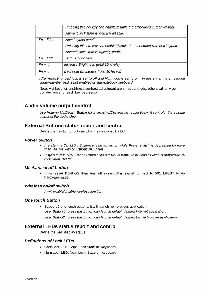
Fn + F10 Cursor keypad on/off.
Pressing this hot key can enable/disable the embedded cursor keypad.
Numeric lock state is logically disable.
Fn + F11 Num keypad on/off
Pressing this hot key can enable/disable the embedded Numeric keypad.
Numeric lock state is logically enable.
Fn + F12 Scroll Lock on/off
Fn + ↑ Increase Brightness (total 10 levels)
Fn + ↓ Decrease Brightness (total 10 levels)
- After rebooting, pad lock is set to off and Num lock is set to on. In this state, the embedded cursor/number pad is not enabled on the notebook keyboard.
Note: Hot keys for brightness/contrast/Volumn up/down adjustment are in repeat mode, others will only be updated once for each key depression.
When the embedded cursor/number pad is on, holding down Fn will turn the embedded cursor/number pad off.
Chapter 2-3
Buttons
Power Button Under ACPI, the power button action is under the control of the operation system.
• The following is a table of the state transitions in ACPI mode.
Initial Final Comments
Off On Does a normal reboot. Prompts for password if required.
Standby On Restores device states from RAM. Prompts for password if required.
Hibernate On Restores RAM and device states from disk. Prompts for password if required.
On Standby, Hibernate(default) or Off
. Action depends on OS setting. Can be set to Standby, Hibernate, or Off(default).
. Note that the Off option is done under the control of the OS, so it is functionally the same as doing a Start-Shut down but probably quicker.
Power Button Over-ride Holding down the Power Button for 4 seconds will cause an unconditional transfer to the Off state without notifying the operating system.
If press power button for less than 4 seconds, the system will enter suspend to RAM or OFF state according to OS UI setting.
Lid Switch This section describes the expected behavior of the system when the lid is opened or closed by the user. If the system is running under legacy mode: • Closing the lid will turn off LCD backlight. If the system is running under ACPI mode:
• The function of lid switch will follow the OS setting in power management (Nothing, standby, Hibernate or Power off). If standby, the system wakes up when the lid opens. If nothing, the backlight must still turn off when the lid is closed.
System status indicators Please refer to Keyboard BIOS specification.
Core BIOS Features Enhanced IDE Disk Drive Support (EDD)
In addition to AT standard disk drive support, the Phoenix NoteBIOS 4.06 also supports: • Auto-detection and sizing of all IDE drives. • Logical Block Addressing(LBA) • Fast DMA support • Ultra DMA-33/66/100 support The CHS translation mode will be used.
Chapter 2-4
Multi Boot The notebook can support Multi Boot for selecting the boot sequence of hard disk, floppy, CD ROM, Network Boot in Setup. It identifies all IPL (Initial Program Load) devices in the system and attempts to boot them in the order specified in Setup.
Quiet Boot Quiet Boot replaces the customary technical messages during POST with a more visually pleasing and comfortable display (OEM Logo screen). During POST, right after the initialization of VGA, The notebook displays an illustration called the OEM screen during system boot instead of the traditional POST screen that displays the normal diagnostic messages.
The OEM Logo screen stays up until just before the operating system loads unless: • Press <Esc> to change the boot order. • Press <F2> to enter Setup. (When pressed, need to show “Entering Setup…”)
• Press <F12> to boot from LAN (When pressed, need to show “Booting from LAN…”)
• Whenever POST detects a non-terminal error, it switches to the POST screen near the end of POST, just prior to prompting for a password.
• If the BIOS or an option ROM requests keyboard input, the system switches over to the POST screen with prompts for entering the information. POST continues from there with the regular POST screen.
New Interrupt 15h extensions The BIOS must support the recently defined standard INT 15 extensions:
Big Memory Big memory support that can reporting greater than 64 megabytes of RAM. The notebook supports the INT 15h big-memory reporting functions of E801h, E881h, and E820h. This feature reports all available extended memory (both below and above the 64MB limit) using both a real mode (E801h) and a 32-bit protected mode (E881h) interface. Operating systems can access the real-mode interface through the standard INT 15h call. They can access the protected-mode interface through a 32-bit interrupt call, much like the EISA protected-mode interface. The Microsoft-defined E820h function returns a complete memory map through a series of repeated calls.
Boot Block The Flash ROM used in many systems today offer the customer the advantage of electronically reprogramming the BIOS without physically replacing the BIOS ROM. This advantage, however, does create a possible hazard: power failures or fluctuations that occur during updating the Flash ROM can damage the BIOS code, making the system unbootable. To prevent this possible hazard, many Flash ROM include a special non-volatile region that can never be erased. This region, called the boot block, contains a fail-safe recovery routine. If the boot block finds corrupted BIOS, it prompts the end user to insert a diskette, from which it loads several files that replace the corrupted BIOS on the Flash ROM with an uncorrupted one.
Plug-n-Play (PnP) Support To achieve the goal of PnP, a POST conflict detection and resolution (CDR) module, and a run-time services module will be integrated into the system BIOS.
The PnP runtime service module includes multiple interfaces so that the system can support the current DOS/Win3.1 non-PnP drivers, as well as Win95 operating system that include specific support for the PnP BIOS specification.
Chapter 2-5
Security Features Security features to be supported are passwords, electronic serial number, PC identification string.
The Electronic Serial Number provides a unique way of identifying an individual notebook.
PC Identification strings allow the user or administrator to personalize the notebook for asset tracking or identification if it is lost.
The Passwords, Serial Number, and PC Identification strings are to be stored in EEPROM.
2 Level Passwords The notebook supports two levels of password protection. The password support consists of a User Password and an Administrator Password. They each contain up to eight characters, and are stored in EEPROM. Using the administration password to enter the setup utility allows the user to access all the configurable fields. Whereas using the user password only allows the user to configure a limited number of fields.
When the password is enabled, the notebook may display a suitable password prompt on the main display in the following situations:.
• Turning on from off states. (No BIOS suspend/resume password)
• Entering to Setup. The User will attempt to enter a password, then press ENTER. If the User fails to enter the password in three tries the system will be halt.
User Password The user can choose:
• The password will never be required
• Be required to boot.
• The user password may not be set unless the administrator password is set. If the user wishes to only have one password then the administrator password is used.
Administrator Password There are three primary uses for the Administrator Password:
• Protect users from changing system configuration that could cause the notebook to malfunction.
• As the users password if only a single password is desired.
Passwords and Setup There are individual checkbox items in Setup to allow the user to specify when to require a password. The wording of these options should be:
Password Required to:
Boot [Enabled]
The following table lists the items in the Setup utility which can be modified by the User.
Time & Date
User password
While setting new password, three failures to enter the old password will result in the system turning off.
Valid Password Characters Valid Password Characters
Chapter 2-6
• The numbers 0 to 9.
• The letters A to Z (not case sensitive). The password is stored as scan codes.
Electronic Serial Number The electronic serial number is a ten (10) byte string which matches the manufacturing serial number on the bottom of the notebook. The BIOS must display the electronic serial number in the boot screen and in Setup. The format of the line should be
Serial Number: SSSSSSSSSS
where SSSSSSSSSS is the electronic serial number. The format of the serial number is:
CCYWWNNNNN
Where
CC is a two character country code (TW for Taiwan).
Y is the year of manufacture (7 = 1997, 8 = 1998, etc.)
WW is the week of manufacture (1 to 52)
NNNNN is the unit number (see below).
Unit number is a number from 00000 to 99999 and is incremented for each unit produced. The unit number is reset at the beginning of each week. Before displaying the serial number, the BIOS must check for the special ′invalid′ serial number (INVALID000). If this special serial number is detected, the BIOS should display the message:
INVALID ELECTRONIC SERIAL NUMBER
ENTER THE SERIAL NUMBER NOW:
The BIOS must then force the user to enter the serial number and program the entered serial number into the EEPROM. The BIOS must perform validity checks on the serial number entered.
System boards sent to service must be preprogrammed with this invalid serial number. This is to insure that when a service technician swaps a new main board into a system that he/she sets the serial number to match the serial number of the system.
This same electronic serial number is used for the serial number returned by the SM BIOS.
Software Password Backdoor Because users occasionally forget their password we need a method of removing the password for them. This method must involve little risk to the security of the password system in general.
The method is that the User calls up Customer Support, Support tells them to press some *special key combination which causes a ′secret code′ to be displayed, the user describes this to support representative who then use their secret decoder ring to generate a ′super-password′ which they tell the user to type in. This removes (deletes) all passwords (user and administrator).
During the password request process, three failed attempts to enter the backdoor password will also cause system turning off.
The back door password process can only be held on the cold boot.
Thermal management There are two types of cooling techniques used for thermal management. The first type is passive cooling where the CPU speed is reduced or other devices power consumption is
Chapter 2-7
reduced in an effort to reduce heat generation. The second type is active cooling where a fan is turned on to cool the system.
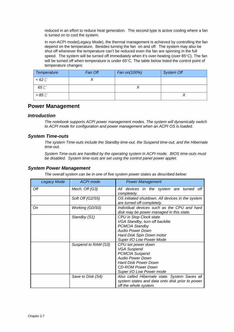
In non-ACPI mode(Legacy Mode), the thermal management is achieved by controlling the fan depend on the temperature. Besides turning the fan on and off. The system may also be shut off whenever the temperature can’t be reduced even the fan are spinning in the full speed. The system will be turned off immediately when it’s over-heating (over 85°C). The fan will be turned off when temperature is under 65°C. The table below listed the control point of temperature changes:
Temperature Fan Off Fan on(100%) System Off
< 62℃ X
65℃ X
> 85℃ X
Power Management Introduction
The notebook supports ACPI power management modes. The system will dynamically switch to ACPI mode for configuration and power management when an ACPI OS is loaded.
System Time-outs The system Time-outs include the Standby time-out, the Suspend time-out, and the Hibernate time-out.
System Time-outs are handled by the operating system in ACPI mode. BIOS time-outs must be disabled. System time-outs are set using the control panel power applet.
System Power Management The overall system can be in one of five system power states as described below:
Legacy Mode ACPI mode Power Management
Off Mech. Off (G3) All devices in the system are turned off completely.
Soft Off (G2/S5) OS initiated shutdown. All devices in the system are turned off completely.
On Working (G0/S0) Individual devices such as the CPU and hard disk may be power managed in this state.
Standby (S1) CPU in Stop Clock state VGA Standby, turn off backlite PCMCIA Standby Audio Power Down Hard Disk Spin Down motor Super I/O Low Power Mode
Suspend to RAM (S3) CPU set power down VGA Suspend PCMCIA Suspend Audio Power Down Hard Disk Power Down CD-ROM Power Down Super I/O Low Power mode
Save to Disk (S4) Also called Hibernate state. System Saves all system states and data onto disk prior to power off the whole system.

Chapter 2-8
Device Power Management The device specific power management supported by this notebook includes the CPU and the hard disk.
CPU power management
• ACPI mode The operating system detects when the system is idle and places the CPU in one of the 3 CPU low power states (C1, C2 or C3) depending on how much latency it believes the system can afford.
The C1 state is simply the CPU halt instruction. The C2 state is the CPU stop grant state. The C3 state is the CPU stop clock state. The CPU stays in this state until an interrupt occurs.
Hard Disk
• ACPI mode Newer OSes use the spin down timer of the hard drive to set time-outs. The user can sets the hard disk spin down time-out in the control panel power applet.
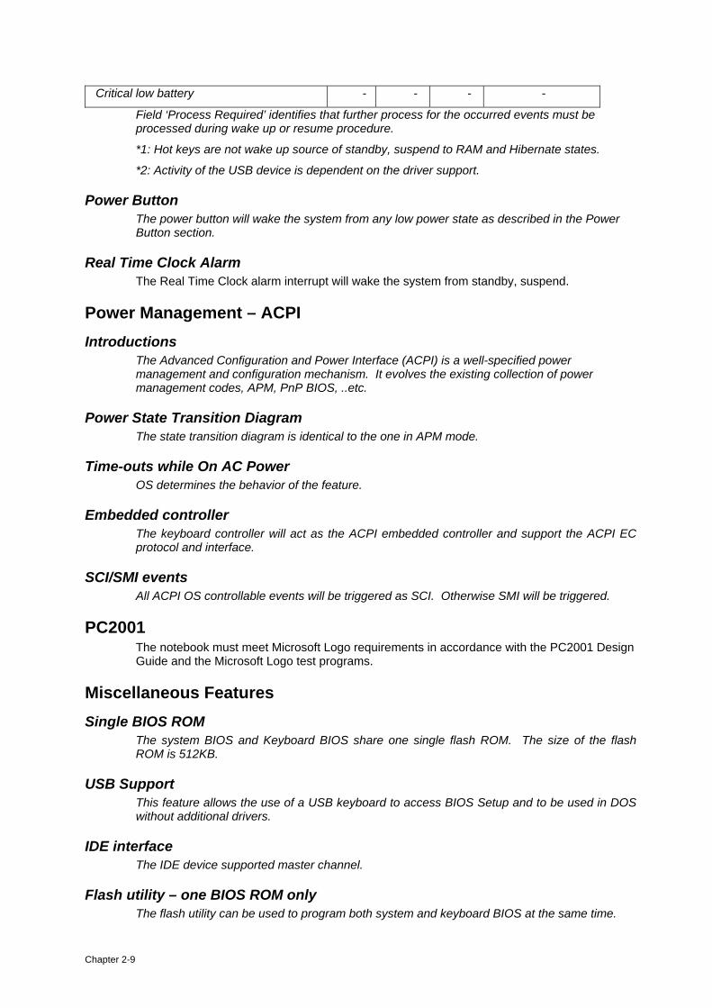
System Wake Up Sources The table below lists the wake up events for all low power states:
Events S1 S3 S4 Process required
Hot Key(*1) - - - -
Power button V V V -
Lid open V V - -
Lid close - - - -
Modem Ring (Mini-PCI Modem) V V - -
Modem Ring (USB/PCMCIA Modem) - - - -
Modem Ring (Serial Port Modem) - - - -
LAN (Mini-PCI NIC) V V - -
LAN (USB/PCMCIA NIC) - - - -
AC/Battery - - - V
Thermal - - - V
RTC V V - -
COM/LPT/KB/Mouse/FDD/HDD - - - -
Audio/Video activity - - - -
PCMCIA - - - Driver
USB(*2) - - - Driver
Module swap---Battery - - - V
Module swap---non Battery - - - V
CRT(no event) plug/unplug - - - V
Hot Plug PS/2 devices - - - KB only
Chapter 2-9
Critical low battery - - - -
Field ‘Process Required’ identifies that further process for the occurred events must be processed during wake up or resume procedure.
*1: Hot keys are not wake up source of standby, suspend to RAM and Hibernate states.
*2: Activity of the USB device is dependent on the driver support.
Power Button The power button will wake the system from any low power state as described in the Power Button section.
Real Time Clock Alarm The Real Time Clock alarm interrupt will wake the system from standby, suspend.
Power Management – ACPI Introductions
The Advanced Configuration and Power Interface (ACPI) is a well-specified power management and configuration mechanism. It evolves the existing collection of power management codes, APM, PnP BIOS, ..etc.
Power State Transition Diagram The state transition diagram is identical to the one in APM mode.
Time-outs while On AC Power OS determines the behavior of the feature.
Embedded controller The keyboard controller will act as the ACPI embedded controller and support the ACPI EC protocol and interface.
SCI/SMI events All ACPI OS controllable events will be triggered as SCI. Otherwise SMI will be triggered.
PC2001 The notebook must meet Microsoft Logo requirements in accordance with the PC2001 Design Guide and the Microsoft Logo test programs.
Miscellaneous Features Single BIOS ROM
The system BIOS and Keyboard BIOS share one single flash ROM. The size of the flash ROM is 512KB.
USB Support This feature allows the use of a USB keyboard to access BIOS Setup and to be used in DOS without additional drivers.
IDE interface The IDE device supported master channel.
Flash utility – one BIOS ROM only The flash utility can be used to program both system and keyboard BIOS at the same time.

Chapter 2-10
EEPROM There is one EEPROM which is used to store many important system and user data in the notebook The size of the EEPROM is 2K bytes.
Password Protection Password and Security support will be implemented in this model. See the PhoenixBIOS 4.0 User Manual for sample screen and the description of Password and Security support.
VGA Support This section describes the expected behavior when a video monitor is connected to the VGA port on the notebook or port replicator.
The BIOS will use both of the RGB and pin 11 methods to determine the presence of an external VGA monitor. Either case meet will indicate an external VGA monitor is present.
The BIOS setup utility will have a menu for setting up the behavior of the external VGA port according to user preference. There are two settings:
Setting 1, AUTO: Auto-select External VGA if attached(CRT only), LCD if external not attached.
Setting 2, BOTH: Both External VGA and LCD always on.
When setting 1 is selected the BIOS will automatically turn the internal display off and the external monitor on, whenever an external monitor is detected. Otherwise it will enter LCD only mode (with the backlite off if the cover lid is closed). This means that the BIOS must check for the external video being present during POST; on resume from standby, on resume from suspend to RAM, on resume from hibernate; on warm dock, on hot dock, on hot undock, and on warm undock.
When setting 2 is selected, the BIOS will always turn on both the internal display and external monitor regardless of whether an external monitor is detected.
The hot key for switching the external video (Fn + F5) must only make a temporary change. It must not change the user′s preference in CMOS, it will just change the current state of the external video port. Also the hot key must not check to see if an external monitor is detected before switching to external only mode. It should just toggle between internal only, both, and external only (without regard to monitor detect). The hot key setting will not survive suspend to RAM, hibernate. In these cases the mode should be set back to the setting stored in CMOS.
Internal Pointing Device Support Added a new BIOS setup to enhance the PS/2 pointing devices
PS/2 Pointing Devices: Auto-Selected: Disable internal pointing devices if external PS/2 mouse is present.
Simultaneous: The internal pointing device is always enabled. Any external pointing device connected will also be enabled at the same time.
• If an external PS/2 mouse is detected, it will be enabled. If USB mice are detected, they will be enabled as well. If an external mouse contains a third mouse button, it will function as expected.
• Double click the Mouse icon in the Windows2000/XP Control Panel to adjust pointer speed, double click speed, right-handed versus left-handed button settings, and pointer appearance. The settings in this applet apply to all the external and internal pointing devices in the system. Except as described below, there are no individual pointing device adjustments available.
• Tapping (or double tapping) on the TouchPad is equivalent to a single (or double) left mouse click. The Synaptics TouchPad driver will be available on the hard drive and the

Chapter 2-11
customer may choose to manually install it. The Synaptics TouchPad driver should only be installed after first selecting Touch pad only in BIOS Setup.
• Hold down center button of external PS/2 mouse: While holding down the center button of an external mouse, move the mouse. This will cause the window to move. If the center button is not held down, all pointing devices function normally.
• Use TouchPad: The TouchPad is locked in as the Scrolling or Magnifying Glass device. Sweeping across the TouchPad causes the window to move. The other pointing devices function normally.
BIOS Version and Resource Allocated BIOS version number
The BIOS version string is in below format:
pppp.x.yy
Where:
pppp Four letter platform descriptor.
x One digit BIOS major revision number.
yy Two digit BIOS minor revision number
Below lists the BIOS version numbers that will be assigned to this platform.
Platform QA Releases Production Release CY25 CY25_0.xx CY25_1.00
NOTE: yy starts at 0 and is incremented with each release of the specific type. During the development and testing of the second release the engineering and QA release will
Configuration Requirements The table below lists the possible usage of the system resources:
IRQ Hardware 00 System Timer
01 Keyboard
02 Programmable Interrupt Controller
03 Free by default or Generic
04 Communications Port (COM1)
05 PCI AUDIO/MODEM
06 Standard Floppy Disk Controller
07 ECP Printer Port (LPT1)
08 Real Time Clock
09 SCI
10 LAN / Universal Serial Bus
11 PCMCIA/VGA
12 Mouse
13 Numeric data processor
14 Primary IDE controller (hard disk)

Chapter 2-12
15 Secondary IDE controller (CD ROM)
DMA Hardware
00 PnP Audio System CODEC
01 Free
02 Standard Floppy Disk Controller
03 ECP Printer Port (default)
System Management BIOS(SM BIOS) version 2.3.1 or greater This product require that SMB 2.3.1 BIOS sub-structures be supported as follows:
TYPE Structure Type Required?
0 BIOS Information YES
1 System Information (Component ID) YES
2 Motherboard Information YES
3 System Enclosure YES
4 Processor Information YES
5 Memory Controller YES
6 Memory Information YES
7 Cache Information YES
8 Port Connector Information YES
9 System Slots YES
10 On Board Devices YES
11 OEM Strings YES
12 System Configuration YES
13 BIOS Language Information NO
14 Group Associations NO
15 System Event Log NO
16 Physical Memory Array YES
17 Memory Devices YES
18 Memory Error Information NO
19 Memory Array Mapped Address YES
20 Memory Device Mapped Address YES
21 Built-in Pointing Device YES
22 Portable Battery YES
23 System Reset NO
24 Hardware Security NO

Chapter 2-13
25 System Power Control NO
26 Voltage Probe NO
27 Cooling Device NO
28 Temperature Probe NO
29 Electrical Curretn Probe NO
30 Out-of-Band Remote Access NO
32 BIOS Intergrity Service YES
126 Inactive NO
127 End-of-Table YES
This product require that the Serial Number field, which is a string at offset 7 of the Type 1 (System Information) sub-structure, is to be filled in with the unit′s Electronic Serial Number. This would be filled in at boot time. Please see section 5.4.2 for information on the Electronic Serial Number.
POST summary screen The Post summary screen is a screen that appears at the end of the POST processing if quiet boot is disabled or the user presses the Esc key during POST. The screen must contain the information listing below:
• A copyright message
• Electronic Serial Number
• UUID number
• The BIOS revision number and model name in customer format At the bottom of the screen, the screen should have the following messages:
Press ESC to change boot order
Press <F2> to enter setup, <F12> to boot from LAN
CMOS RAM management The BIOS will automatically update certain information in CMOS on each boot. This information includes:
• DRAM size and configuration
• Hard disk configuration
• Always report the existence of one FDD. If the CMOS RAM fails checksum or a power lost on CMOS battery is detected during boot, an appropriate error message will be displayed:
System CMOS checksum bad – Default configuration used
The system BIOS must automatically load default values defined in the setup menu during POST when encounter these problems. The user must not be required to take any action to continue the rest of POST(or entering SETUP).
Diskless Boot This feature allows the system to boot off of a LAN when the hard disk is absent or has not been loaded with the operating system. It is utilized by the software download process in manufacturing. This product will use PXE since this is a PC2001 requirement.
Chapter 2-14
System Setup Invoking setup
The setup function can only be invoked by pressing F2 when ″ Press <F2> to enter Setup″ message is prompted on the bottom of screen during POST.
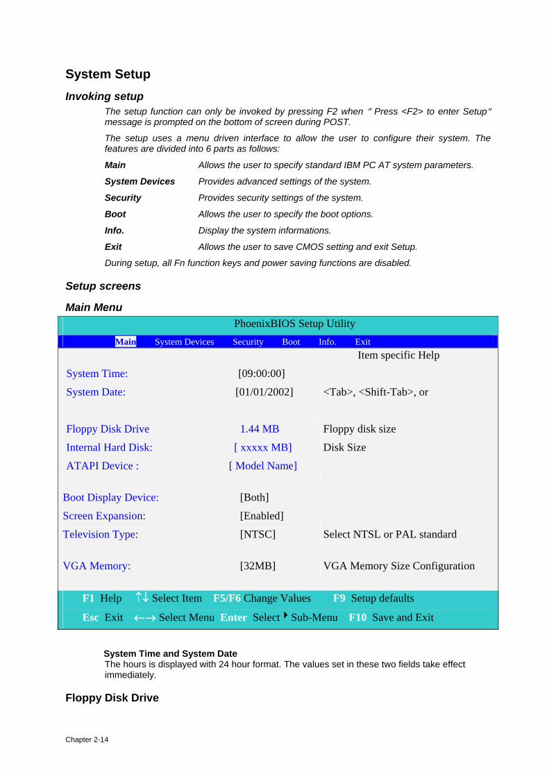
The setup uses a menu driven interface to allow the user to configure their system. The features are divided into 6 parts as follows:
Main Allows the user to specify standard IBM PC AT system parameters.
System Devices Provides advanced settings of the system.
Security Provides security settings of the system.
Boot Allows the user to specify the boot options.
Info. Display the system informations.
Exit Allows the user to save CMOS setting and exit Setup.
During setup, all Fn function keys and power saving functions are disabled.
Setup screens
Main Menu PhoenixBIOS Setup Utility
Main System Devices Security Boot Info. Exit Item specific Help
System Time: [09:00:00]
System Date: [01/01/2002] <Tab>, <Shift-Tab>, or
Floppy Disk Drive 1.44 MB Floppy disk size
Internal Hard Disk: [ xxxxx MB] Disk Size
ATAPI Device : [ Model Name]
Boot Display Device: [Both]
Screen Expansion: [Enabled]
Television Type: [NTSC] Select NTSL or PAL standard
VGA Memory: [32MB] VGA Memory Size Configuration
F1 Help ↑↓ Select Item F5/F6 Change Values F9 Setup defaults
Esc Exit ←→ Select Menu Enter Select4Sub-Menu F10 Save and Exit
System Time and System Date
The hours is displayed with 24 hour format. The values set in these two fields take effect immediately.
Floppy Disk Drive
Chapter 2-15
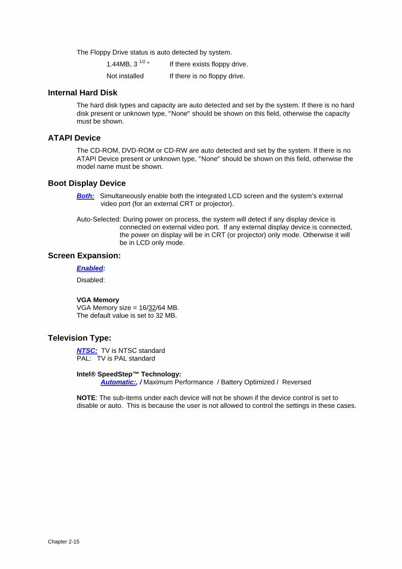
The Floppy Drive status is auto detected by system.
1.44MB, 3 1/2 “ If there exists floppy drive.
Not installed If there is no floppy drive.
Internal Hard Disk The hard disk types and capacity are auto detected and set by the system. If there is no hard disk present or unknown type, ″None″ should be shown on this field, otherwise the capacity must be shown.
ATAPI Device
The CD-ROM, DVD-ROM or CD-RW are auto detected and set by the system. If there is no ATAPI Device present or unknown type, ″None″ should be shown on this field, otherwise the model name must be shown.
Boot Display Device
Both: Simultaneously enable both the integrated LCD screen and the system’s external video port (for an external CRT or projector).
Auto-Selected: During power on process, the system will detect if any display device is
connected on external video port. If any external display device is connected, the power on display will be in CRT (or projector) only mode. Otherwise it will be in LCD only mode.
Screen Expansion: Enabled:
Disabled:
VGA Memory VGA Memory size = 16/32/64 MB. The default value is set to 32 MB.
Television Type:
NTSC: TV is NTSC standard PAL: TV is PAL standard
Intel® SpeedStep™ Technology:
Automatic:, / Maximum Performance / Battery Optimized / Reversed
NOTE: The sub-items under each device will not be shown if the device control is set to disable or auto. This is because the user is not allowed to control the settings in these cases.
Chapter 2-16
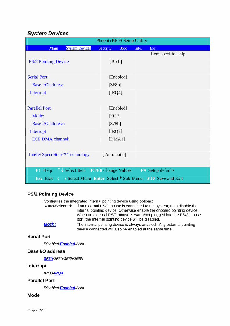
System Devices PhoenixBIOS Setup Utility
Main System Devices Security Boot Info. Exit Item specific Help
PS/2 Pointing Device [Both]
Serial Port: [Enabled]
Base I/O address [3F8h]
Interrupt [IRQ4]
Parallel Port: [Enabled]
Mode: [ECP]
Base I/O address: [378h]
Interrupt [IRQ7]
ECP DMA channel: [DMA1]
Intel® SpeedStep™ Technology [ Automatic]
F1 Help ↑↓ Select Item F5/F6 Change Values F9 Setup defaults
Esc Exit ←→ Select Menu Enter Select4Sub-Menu F10 Save and Exit
PS/2 Pointing Device Configures the integrated internal pointing device using options: Auto-Selected: If an external PS/2 mouse is connected to the system, then disable the
internal pointing device. Otherwise enable the onboard pointing device. When an external PS/2 mouse is warm/hot plugged into the PS/2 mouse port, the internal pointing device will be disabled.
Both: The internal pointing device is always enabled. Any external pointing device connected will also be enabled at the same time.
Serial Port Disabled/Enabled/Auto
Base I/O address 3F8h/2F8h/3E8h/2E8h
Interrupt IRQ3/IRQ4
Parallel Port Disabled/Enabled/Auto
Mode
Chapter 2-17
Normal/Bi-directional/ECP/EPP
Base I/O address 378h/278h/3BCh
Interrupt IRQ 5/IRQ 7
ECP DMA channel: This field is hidden if Mode is not ECP
DMA 1/DMA 3
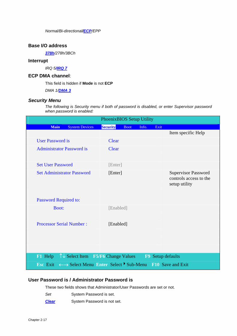
Security Menu The following is Security menu if both of password is disabled, or enter Supervisor password when password is enabled:
PhoenixBIOS Setup Utility Main System Devices Security Boot Info. Exit
Item specific Help
User Password is Clear
Administrator Password is Clear
Set User Password [Enter]
Set Administrator Password [Enter] Supervisor Password controls access to the setup utility
Password Required to:
Boot: [Enabled]
Processor Serial Number : [Enabled]
F1 Help ↑↓ Select Item F5/F6 Change Values F9 Setup defaults
Esc Exit ←→ Select Menu Enter Select4Sub-Menu F10 Save and Exit
User Password is / Administrator Password is These two fields shows that Administrator/User Passwords are set or not.
Set System Password is set.
Clear System Password is not set.

Chapter 2-18
Set User Password / Set Administrator Password Enter This field always shows the message.
While these fields are highlighted and press ′Enter′, a window similar to the following is shown:
Set Administrator Password
Enter New Password [ ]
Confirm New Password [ ]
If there is an old password then setup will prompt with the following window instead and a current password will be required to be entered at first:
Set Administrator Password
Enter current password [ ]
Enter New Password [ ]
Confirm New Password [ ]
User can now type password in field ″Enter New Password″, and re-enter password in field ″ Confirm New Password ″ for verification.
If the verification is OK:
Setup Notice
Changes have been saved.
[ continue]
The password setting is complete after user presses enter.
If the current password entered does not match the actual current password:
Setup Warning
Invalid password
Re-enter Password
[ continue]
If the new password and confirm new password strings do not match:
Setup Warning
Password do not match
Re-enter Password
The format of the password is as follows:
Length No more than 8 characters.

Chapter 2-19
Characters 0-9, A-Z (not case sensitive)
Password Required to Defines whether a password is required or not while the events defined in this group happened. The following sub-options are all requires the Administrator password for changes and should be grayed out if the user password was used to enter setup.
Boot Allows the user to specify whether or not a password is required to boot.
Disabled/Enabled
Boot Menu This menu allows the user to decide the order of boot devices to load the operating system. Bootable devices includes the diskette drive in module bay, the onboard hard disk drive and the CD-ROM in module bay.
PhoenixBIOS Setup Utility Main System Devices Security Boot Info. Exit
Item specific Help
1. Hard Disk
2. CD-ROM/DVD Drive
3. Floppy
4. Network Boot
Use <↑> or <↓> to select a device, then press <F6> to move it up the List, or <F5> to move it down the list. Press <Esc> to escape the menu
F1 Help ↑↓ Select Item F5/F6 Change Values F9 Setup defaults
Esc Exit ←→ Select Menu Enter Select4Sub-Menu F10 Save and Exit
Chapter 2-20
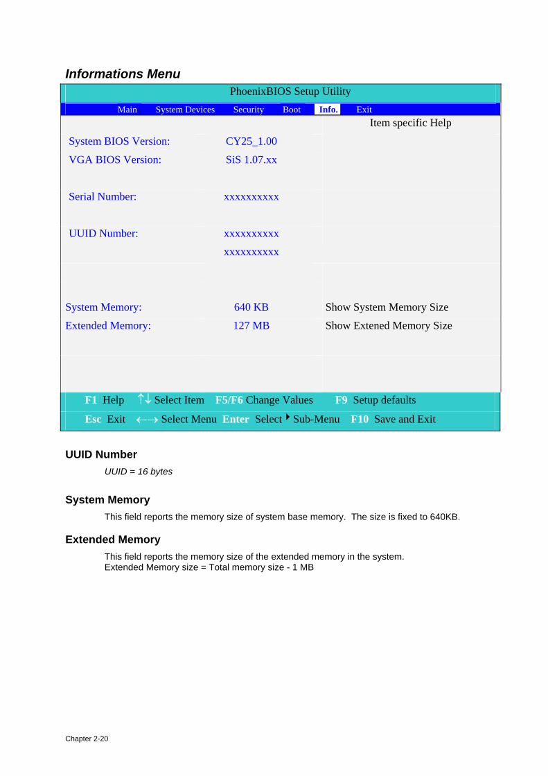
Informations Menu PhoenixBIOS Setup Utility
Main System Devices Security Boot Info. Exit Item specific Help
System BIOS Version: CY25_1.00
VGA BIOS Version: SiS 1.07.xx
Serial Number: xxxxxxxxxx
UUID Number: xxxxxxxxxx
xxxxxxxxxx
System Memory: 640 KB Show System Memory Size
Extended Memory: 127 MB Show Extened Memory Size
F1 Help ↑↓ Select Item F5/F6 Change Values F9 Setup defaults
Esc Exit ←→ Select Menu Enter Select4Sub-Menu F10 Save and Exit
UUID Number UUID = 16 bytes
System Memory
This field reports the memory size of system base memory. The size is fixed to 640KB.
Extended Memory This field reports the memory size of the extended memory in the system. Extended Memory size = Total memory size - 1 MB
Chapter 2-21
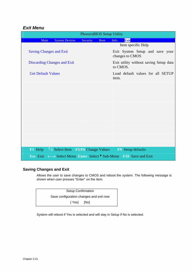
Exit Menu PhoenixBIOS Setup Utility
Main System Devices Security Boot Info. Exit Item specific Help
Saving Changes and Exit Exit System Setup and save your changes to CMOS
Discarding Changes and Exit Exit utility without saving Setup data to CMOS.
Get Default Values Load default values for all SETUP item.
F1 Help ↑↓ Select Item F5/F6 Change Values F9 Setup defaults
Esc Exit ←→ Select Menu Enter Select4Sub-Menu F10 Save and Exit
Saving Changes and Exit Allows the user to save changes to CMOS and reboot the system. The following message is shown when user presses ″Enter″ on the item.
Setup Confirmation
Save configuration changes and exit now
[ Yes] [No]
System will reboot if Yes is selected and will stay in Setup if No is selected.
Chapter 2-22
Discarding Changes and Exit Allows the user to not save changes before exiting Setup. The following message is shown when user presses ″Enter″ on this item.
Warning
Configuration has not been saved!
Save before exiting?
[Yes] [No]
System will reboot after either selection.
Get Default Values Allows the user to load default values in CMOS Setup. The following message is shown when user presses ″Enter″ on this item:
Setup Confirmation
Load default configuration now?
[ Yes] [No]
It still stay in Setup after either selection.
OS Compatibility OS Retail Support
MS-DOS Minimal (Diagnostics and Manufacturing utilities)
Microsoft XP Home Edition Full
Microsoft XP Professional Edition Full
Microsoft Windows 2000 Not supported
Microsoft Windows Millennium Not supported
Microsoft Windows 98 Second Edition (ACPI only)
Not supported
Microsoft Windows NT 4.0 SP5+ Not supported
Chapter 2-23
Software Specification for KB-BIOS
General purpose This document define the EC specification with standard interface and also define the special feature for OEM function .It’s useful for software engineer to access EC status,and for SA test guide.
Features • Advanced Power Management 1.2 support • ACPI1.0 b and PC2001 compliant • Support SMBus specification V1.0 • Hot keys for system control • Audio volume output control • External LED control • Battery scope report and control • Battery learning support • Sticky key support • Power switch control • Speaker control • Port replicator • Extra key emulation • Two host interface channels support • Supports three independent devices • Devices Hot Plug-and Play/Hot swapping configuration • Internal Keyboard country selection
Types of KB-BIOS provided • Standard version Support for US(87)/UK(88)/Japanese(90) keyboard. KB-BIOS command support with SYSTEM-BIOS
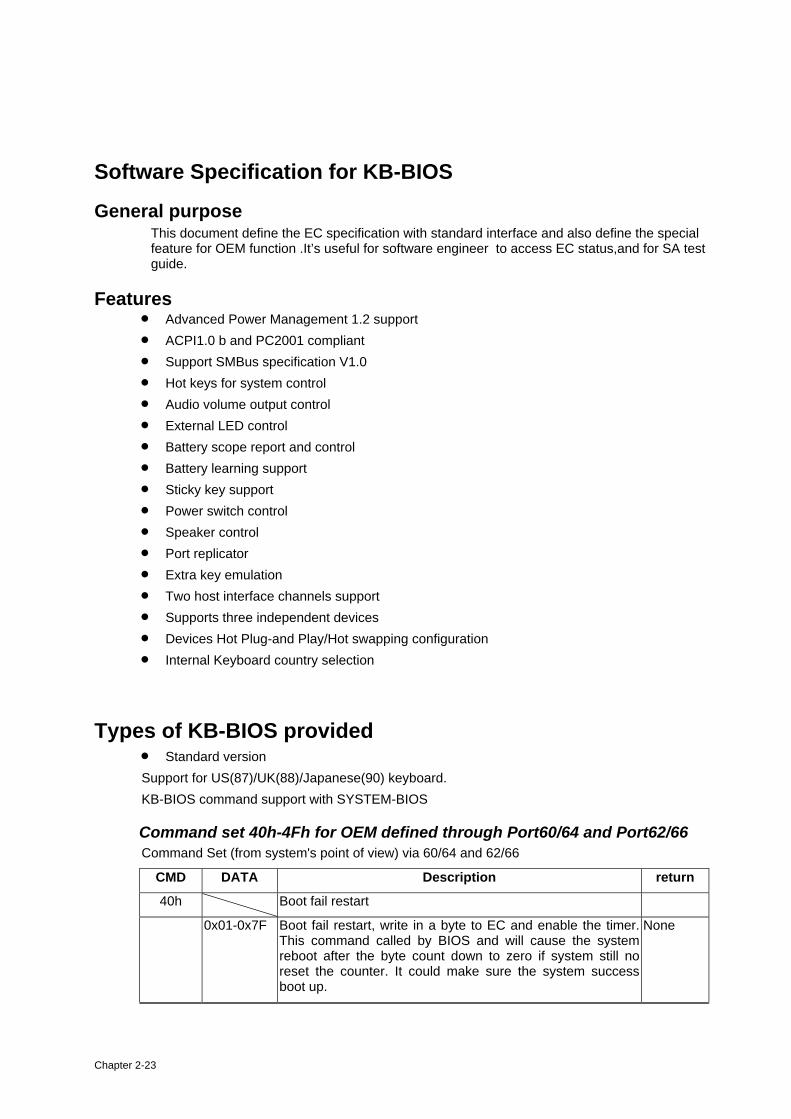
Command set 40h-4Fh for OEM defined through Port60/64 and Port62/66 Command Set (from system's point of view) via 60/64 and 62/66
CMD DATA Description return
40h Boot fail restart
0x01-0x7F Boot fail restart, write in a byte to EC and enable the timer. This command called by BIOS and will cause the system reboot after the byte count down to zero if system still no reset the counter. It could make sure the system success boot up.
None

Chapter 2-24
CMD DATA Description return
41h EC state notification
A0h Return core code version number One byte
A1h Return platform id ‘COMPAL’
42h Bank assign for EEPROM None
0x00-0x07 Bank assign for EEPROM,work with 4D/4E command replace 4B/4C command
None
43h 00h - FFh Get RAM value from EC, Host can use this command to send address to get OEM RAM value. The address range are from 00h to DFh.
1 WORD
0x19 Get PANEL ID Panel id
44h None Get project ID 0x12
45h Hook for every projects NONE
46h fan speed read
01h fan speed 1
N = 60M/return value( rotate one circle 4 pulses)
N = 120M/return value( rotate one circle 2 pulses)
2 bytes
(high byte,
low byte)
02h Fan speed 2
N = 60M/return value( rotate one circle 4 pulses)
N = 120M/return value( rotate one circle 2 pulses)
2 bytes
(high byte
low byte)
47h Speaker mute On/Off
A7h Mute off None
A8h Mute on None
48h Reserved for docking control None
49h Thermal control notification
A0h Fan off None
A1h Fan speed level 1 None
A2h Fan speed level 2 None
A3h HCT enable None
49h A5h Fan speed level 4 None
4Ah Auto into S2R(Delay about 4 Secs) or S2D and resume by timeout, This command provided engineer to verify S2R or S2D and resume function is OK or not
Resume count(second base ), Range is from 0x02 to 0x7F
Bit7 = 0 -> Enabled S2R function
1 -> Enabled S2D function
0x02-0x7F Enabled S2R function None
0x80-0xFF Enabled S2D function None
Chapter 2-25
CMD DATA Description return
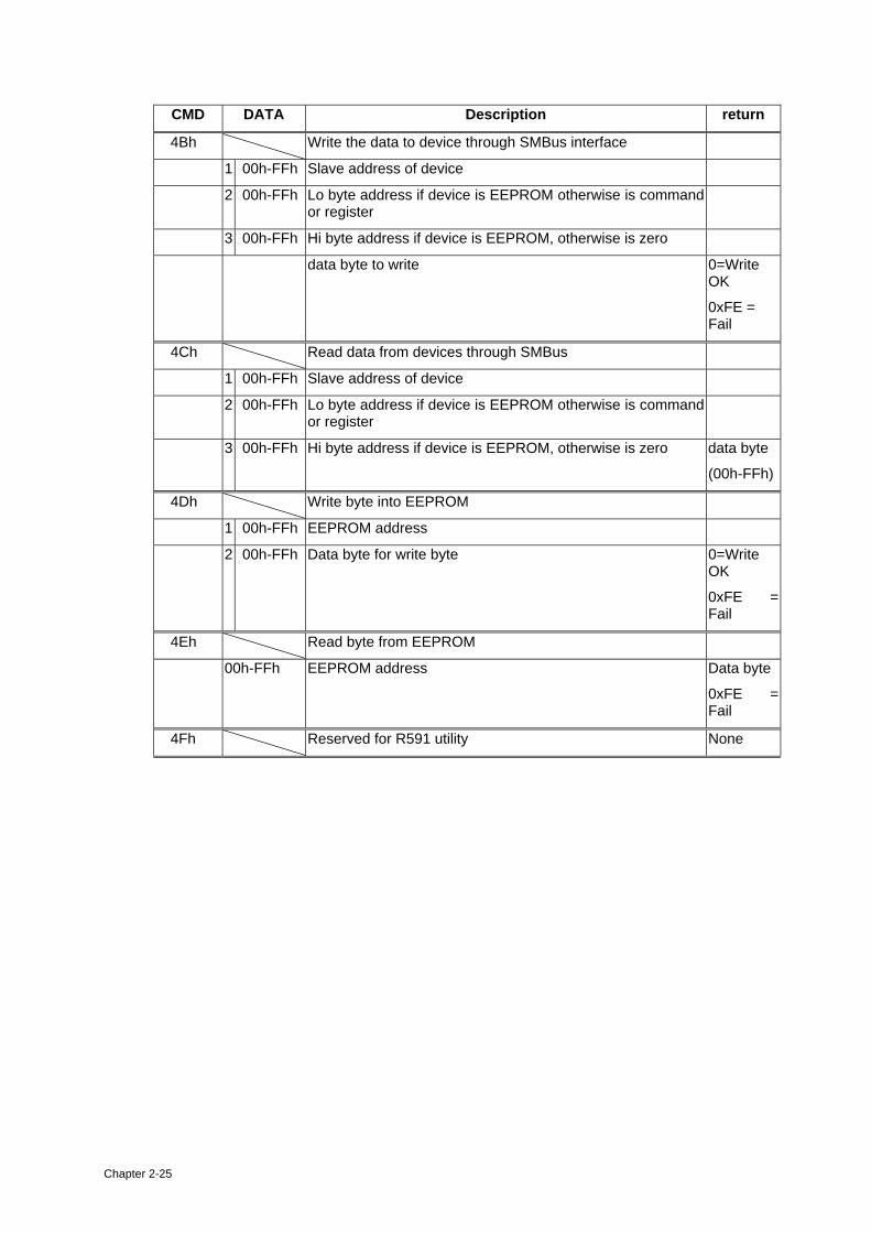
4Bh Write the data to device through SMBus interface
1 00h-FFh Slave address of device
2 00h-FFh Lo byte address if device is EEPROM otherwise is command or register
3 00h-FFh Hi byte address if device is EEPROM, otherwise is zero
data byte to write 0=Write OK
0xFE = Fail
4Ch Read data from devices through SMBus
1 00h-FFh Slave address of device
2 00h-FFh Lo byte address if device is EEPROM otherwise is command or register
3 00h-FFh Hi byte address if device is EEPROM, otherwise is zero data byte
(00h-FFh)
4Dh Write byte into EEPROM
1 00h-FFh EEPROM address
2 00h-FFh Data byte for write byte 0=Write OK
0xFE = Fail
4Eh Read byte from EEPROM
00h-FFh EEPROM address Data byte
0xFE = Fail
4Fh Reserved for R591 utility None

Chapter 2-26
Command set 50h-5Fh for OEM defined through Port60/64 and Port62/66 Command Set (from system's point of view) via 60/64 and 62/66
CMD DATA Description return
50h None Get Docking status. A0h = No dock
A6h = simple docked
51h None Get revision number of KB-BIOS BIOS Rev. 3 bytes
byte0 :
bit0-bit2 = major number(0-7)
bit3-bit7 = type of KB-BIOS
e.g. 0 = A, 1=B and so on..
byte1
minor revision number(0-9)
byte2
If it is 00h then system display “ROM”,other It is “T01” if it is 01h and so on.. .
52h None Hook for every projects(Get platform ID) 5Bytes “ACY25”
53h None Reserved None
54h 0x00-0xFF EC CMOS RAM read Data byte from CMOS
55h EC CMOS RAM write
0x00-0xFF CMOS address offset
0x00-0xFF data byte 0x00 => pass
0x01 => fail
56h Get SMI trigger source One byte
Battery status change 80h
Ask suspend(On mode) A0h
brightness level update A1h
contrast level update A2h
audio volume decreased A3h
audio volume increased A4h
Lid open A5h
Lid closed A6h
External device plugged A7h
External device removed A8h

Chapter 2-27
CMD DATA Description return
Bluetooth wake up event A9h
Bluetooth switch event Aah
Scr expand event Abh
56h Cpu fast event Adh
Cpu slow event Aeh
Pop up event Afh
Resume request from suspend B0h
Ask time out event B1h
Battery life in critical low state B2h
Battery life in low power state B3h
Standby request B4h
Battery Plug-In B5h
Battery Plug-Out B6h
Reserved B7h
Suspend to RAM request B8h
Save to DISK request B9h
Docked request Bah
Undock request Bbh
Reserved Bch
Thermal change event Bdh
Write LM75 event Beh
SMBus event Bfh
Password event C0h
mute function toggle C1h
Power button pressed C2h
TV out toggle C3h
Beep Alarm event C4h
Reserved C5h
Change use battery C6h
AC power plug-in C7h
AC power plug-out C8h
IR toggle event C9h
Modem Ring In Cah
Unload OS Ultra Base Devices Cbh
Surprise undock event Cch
Battery polling Cdh
PME signal active Ceh

Chapter 2-28
CMD DATA Description return
Mouse hot plug event Cfh
56h CRT plug in/out event D0h
Sleep button event D1h
RTC date/time update event D2h
Device change event F0h
Bluetooth lan event F1h
no event FFh
57h None Module identification One byte
bit0 : Ext. FDD exis
bit1 : Int. FDD exist
bit2 : IDE exist
other bit : Reserved
58h 0x00-0xFF Set flat panel type None
59h System state notification None
70h Sticky key mode enable None
71h Sticky key mode disable None
80h start to get LCD status panel information from EEPROM
None
90h One touch button application allow to send scan code(user button) if user pressed
None
91h One touch button application don’t allow to send scan code(user button) if user pressed
None
92h Mail message is waiting(no support in Hurricane)
None
93h Mail message end of waiting(no support in Hurricane)
None
94h Mute on None
95h Mute off None
9Ah Ac off(cut off AC power) None
9bh Ac on None
A2h System enter S2D(S4) state None
A3h System enter beep mode for battery LB state in CMOS setup
None
A4h System enter quiet mode for battery LB state in CMOS setup
None
A5h Fan control by EC None
A8h Fan control by OS None
A9h external PS2 only None
Chapter 2-29
CMD DATA Description return
Aah Both enable external PS2 and internal touch pad
None
Ach Auto enable/disable external PS2 and internal touch pad
None
B1h System into standby None
B2h Resume from standby None
B5h VGA suspend enable None
B6h VGA suspend disable None
B8h Modem ring disable None
B9h PME enable None
Bah PME disable None
Bbh S4 status bit clear None
Bch S4 status bit set None
C1h force battery pack auto learning None
C2h disable battery pack learning None
C3h SMI/SCI Trigger event enable None
C4h SMI/SCI Trigger event disable None
Cbh PCMCIA suspend disable None
Cch PCMCIA suspend enable None
Cdh Wake up LAN disable None
Ceh Wake up LAN enable None
D0h Disable IRQ1 None
D1h Enable IRQ 1
D2h Beep alarm 100mS None
D5h PCMCIA reset off None
D6h PCMCIA reset on None
E1h Turn LCD back-light on None
E2h Turn LCD back-light off None
E5h Select US keyboard Matrix None
E6h Select JP keyboard Matrix None
E7h Select UK keyboard Matrix None
E8h EC into ACPI mode None
E9h Non-ACPI mode (EC default) None
F2h disable watchdog None
F3h enable watchdog None
F4h enable RTC access by EC None
F5h disable RTC access by EC None
F6h Clear header of Boot code None
Chapter 2-30
CMD DATA Description return
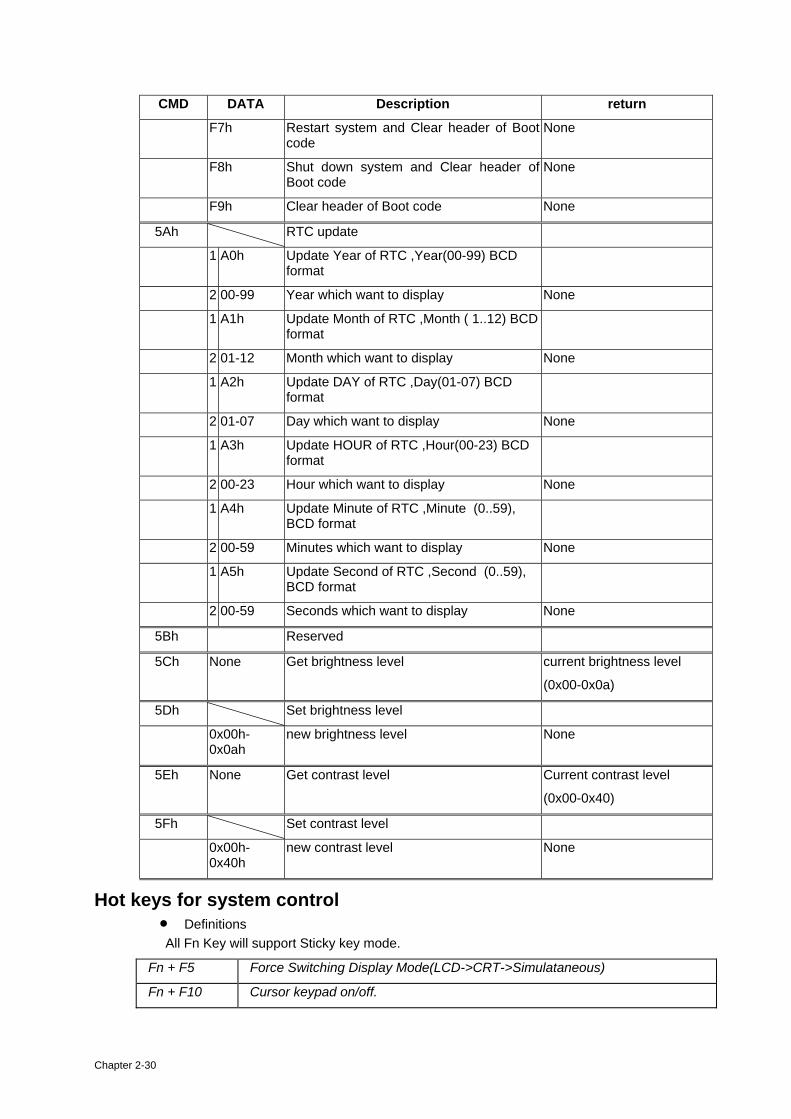
F7h Restart system and Clear header of Boot code
None
F8h Shut down system and Clear header of Boot code
None
F9h Clear header of Boot code None
5Ah RTC update
1 A0h Update Year of RTC ,Year(00-99) BCD format
2 00-99 Year which want to display None
1 A1h Update Month of RTC ,Month ( 1..12) BCD format
2 01-12 Month which want to display None
1 A2h Update DAY of RTC ,Day(01-07) BCD format
2 01-07 Day which want to display None
1 A3h Update HOUR of RTC ,Hour(00-23) BCD format
2 00-23 Hour which want to display None
1 A4h Update Minute of RTC ,Minute (0..59), BCD format
2 00-59 Minutes which want to display None
1 A5h Update Second of RTC ,Second (0..59), BCD format
2 00-59 Seconds which want to display None
5Bh Reserved
5Ch None Get brightness level current brightness level
(0x00-0x0a)
5Dh Set brightness level
0x00h-0x0ah
new brightness level None
5Eh None Get contrast level Current contrast level
(0x00-0x40)
5Fh Set contrast level
0x00h-0x40h
new contrast level None
Hot keys for system control • Definitions All Fn Key will support Sticky key mode.
Fn + F5 Force Switching Display Mode(LCD->CRT->Simulataneous)
Fn + F10 Cursor keypad on/off.
Chapter 2-31
Pressing this hot key can enable/disable the embedded cursor keypad.
Numeric lock state is logically disable.
Fn + F11 Num keypad on/off
Pressing this hot key can enable/disable the embedded Numeric keypad.
Numeric lock state is logically enable.
Fn + F12 Scroll Lock on/off
Fn + ↑ Increase Brightness (total 10 levels)
Fn + ↓ Decrease Brightness (total 10 levels)
After rebooting, pad lock is set to off and Num lock is set to on. In this state, the embedded cursor/number pad is not enabled on the notebook keyboard.
Note: Hot keys for brightness/contrast adjustment are in repeat mode, others will only be updated once for each key depression.
Audio volume output control Use Volumn Up/Down Button for Increasing/Decreasing respectively, it controls the volume output of the audio chip.
External Buttons status report and control Define the function of buttons which is controlled by EC.
Power Switch • If system is Off/S2D : System will be turned on while Power switch is depressed by more
than 500 ms with or without AC insert
• If system is in S2R/Standby state : System will resume while Power switch is depressed by more than 100 ms
Mechanical off button • It will reset KB-BIOS then turn off system.This signal connect to 591 LREST to do
hardware reset.
Wireless on/off switch It will enable/disable wireless function.
One touch Button • Support 2 one touch buttons, it will launch homologous application.
User Button 1: press this button can launch default defined Internet application.
User Button2 : press this button can launch default defined E-mail browser application.
External LEDs status report and control Define the Led display status.
Definitions of Lock LEDs • Caps lock LED: Caps Lock State of Keyboard • Num Lock LED: Num Lock State of Keyboard
Chapter 2-32
Definitions of System state LED • There is one dual-color LED indicator both of Green and Amber color • Green color support for System state. The definition is in below:
Green color activity : System On. Green color off : System Off.
• Amber color support for power management state. The definition is below: • Amber color activity : System in sleep(S1 state) or S2R mode(S3 state).
Color off : Not in power management mode.
Definitions of DC-DC state LED • Green color : for battery charging state.
Green color activility:Battery charging with AC(green LED on for 1sec per 4 sec)
Green color on : Battery full by AC charge.
Green color off : Battery full/discharge
• Amber color(Green and Red) : for battery discharge state.
Amber color activility : batterywithin low state(remain 12 minutes left)
Amber color blinking : battery in critical low state( remain 3 minutes left).
LED flash once per second.
Amber color off : Battery charging
• Red color : Stop charge by battery Bad cell, Over temperature or charging protection.
Definitions of Wireless on/off State LED • Blue color: Wireless power on. • Off: Wireless power off.
Battery status report and control Define the battery type spec and battery protection function.
Battery status • There are four battery states for each battery pack depend on getting the battery state
through SMBus protocol from Smart battery pack: full, normal, low, critical low.
• The battery gas-gauge and level of low power states should base on ‘current’ system configuration.
• Battery turn on system condition : gasgauge > 5%

Chapter 2-33
Battery discharge/charging control Charging Dischargung Action
Charging :0℃<T<50℃
Stop charging:T>60℃
Stop charging
&
Red Led on
T>73℃ T>73℃
T>73℃
Shut down
R.S.O.C. ≦10% LB(Beeping)
R.S.O.C. < 3% LLB
Dependent on OS
TBD LLC
Shut down System
R.S.O.C < 5% during system is in S2R mode.
S2D
Fast Charge Time out: 8 Hours
Trickle Charge Time Out:
1 Hour.
Battery BAD
&
Red Led on
TBD
OverVoltage
&
Red Led on
In ACPI mode
• System should 'Save to Disk'(S2D) or beeping(Low condition) depend on OS setting .
Battery type • The KB-BIOS will support for smart battery pack by SMBus protocol.
• ACPI1.0b and PC2001 Compliant,with PC2001 spec “A mobile system must use a Smart Battery or an ACPI control method battery”,our currently design is ACPI control method battery.
Li-ion Battery : 14.8V/3900mAH (4S2P)
14.8V/4000mAH(4S2P) Ni-MH Battery : No Support
• Compatible with Intel’s SMBus and Philip’s I2C bus protocol.
KB-BIOS Power management support EC will support S1(sleep mode),S3(standby mode),S4(suspend to disk) mode to save the power comsumption.
Chapter 2-34
Power states • Sleep mode LCD panel back-light off
• Save to RAM keyboard(int./ext.) scanning off
• Save to DISK no actions except turning off system with AC exist or turn off KBC without AC.
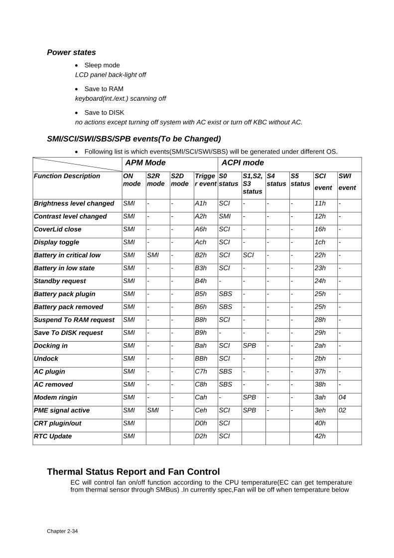
SMI/SCI/SWI/SBS/SPB events(To be Changed) • Following list is which events(SMI/SCI/SWI/SBS) will be generated under different OS.
APM Mode ACPI mode Function Description ON
mode S2R mode
S2D mode
Trigger event
S0 status
S1,S2,S3 status
S4 status
S5 status
SCI
event
SWI
event
Brightness level changed SMI - - A1h SCI - - - 11h -
Contrast level changed SMI - - A2h SMI - - - 12h -
CoverLid close SMI - - A6h SCI - - - 16h -
Display toggle SMI - - Ach SCI - - - 1ch -
Battery in critical low SMI SMI - B2h SCI SCI - - 22h -
Battery in low state SMI - - B3h SCI - - - 23h -
Standby request SMI - - B4h - - - - 24h -
Battery pack plugin SMI - - B5h SBS - - - 25h -
Battery pack removed SMI - - B6h SBS - - - 25h -
Suspend To RAM request SMI - - B8h SCI - - - 28h -
Save To DISK request SMI - - B9h - - - - 29h -
Docking in SMI - - Bah SCI SPB - - 2ah -
Undock SMI - - BBh SCI - - - 2bh -
AC plugin SMI - - C7h SBS - - - 37h -
AC removed SMI - - C8h SBS - - - 38h -
Modem ringin SMI - - Cah - SPB - - 3ah 04
PME signal active SMI SMI - Ceh SCI SPB - - 3eh 02
CRT plugin/out SMI D0h SCI 40h
RTC Update SMI D2h SCI 42h
Thermal Status Report and Fan Control EC will control fan on/off function according to the CPU temperature(EC can get temperature from thermal sensor through SMBus) .In currently spec,Fan will be off when temperature below
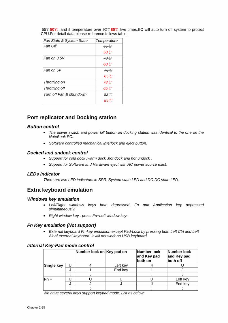
Chapter 2-35
55℃50℃ ,and if temperature over 92℃85℃ five times,EC will auto turn off system to protect CPU.For detail data please reference follows table.
Fan State & System State Temperature Fan Off 55℃
50℃ Fan on 3.5V 70℃
60℃ Fan on 5V 76℃
65℃ Throttling on 78℃ Throttling off 65℃ Turn off Fan & shut down 92℃
85℃
Port replicator and Docking station Button control
• The power switch and power kill button on docking station was identical to the one on the NoteBook PC.
• Software controlled mechanical interlock and eject button.
Docked and undock control • Support for cold dock ,warm dock ,hot dock and hot undock . • Support for Software and Hardware eject with AC power source exist.
LEDs indicator There are two LED indicators in SPR: System state LED and DC-DC state LED.
Extra keyboard emulation Windows key emulation
• Left/Right windows keys both depressed: Fn and Application key depressed simultaneously.
• Right window key : press Fn+Left window key.
Fn Key emulation (Not support) • External keyboard Fn-key emulation except Pad-Lock by pressing both Left Ctrl and Left
Alt of external keyboard. It will not work on USB keyboard.
Internal Key-Pad mode control Number lock on Key pad on Number lock
and Key pad both on
Number lock and Key pad both off
U 4 Left key 4 U J 1 End key 1 J
Single key
: : : : : U U U U Left key J J J J End key
Fn +
: : : : : We have several keys support keypad mode. List as below:
Chapter 2-36
“ 7“,” 8“,” 9“,” 0“,” U”,” I”,” O”,” P”,” J”,” K”,” L”,” ;”,” M”,” .”,” /”.
Other Fn key • Scroll lock :press Fn + F12 • Numeric keypad lock: Fn + F11 • Pad lock: Fn + F10
Two host interface channels support Keyboard and mouse interface transfer port
• One channel is dedicated for the keyboard and mouse data transfer(host address 60h and 64h). The Keyboard and Mouse channel of KBC is compatible to the legacy 8042 host interface. It is base on two registers: Command/Data and Status
• The KB-BIOS interrupt generates IRQ1(Keyboard) and IRQ12(Mouse) for system.
Power management interface transfer port • The other for the power management function(host address 62h and 66h). The Power
Management channel of KBC structure and operation are similar to those of the Keyboard/Mouse channel.
Support three independent devices • The KBC provides three data transfer channels. Each channel has two quasi-bidirectional
signals that are used for the direct interface to an external keyboard, mouse or any other PS/2 compatible pointing device.
• The three channels are identical and thus allow the connector ports to be interchangeable.
Devices PnP configuration Hot Plug-and-Play support
• The KBC watches both external devices, checking if the devices have recently been plugged in or unplugged. The Hot pluggability of external PS2 devices feature detects the attachment or removal of these devices.
Hot swapping control • When the device is plugged in, the software automatically initializes the state of that
device, checks port swapping, and setup the KBC to handle dual-device operation. In dual-device operation, the internal device is set in the same state as external device. When the external device is unplugged, the internal device becomes the primary device.
ACPI EC interface Specification support ACPI interface support
• The KBC provides support for Advance Configuration and Power Interface specification(ACPI) Embedded Controller interface.
EC command support • The 2nd (Power Management) host interface channel of the KBC is dedicated to this
function.
• All EC commands defined in the ACPI specification - Read/Write, Burst Mode enable/disable and Query command - are supported.
Chapter 2-37
Internal keyboard change Configuration US/UK/JP country option
• The KBC supports three country selection by KBD_SEL application.
• You can key in KBD_SEL get the syntax for your option at DOS prompt.
Sticky key support • Press shift key 5 times will enable sticky key function.Turns on StickyKeys,which allows
you to press a modifier key(CTRL,ALT,or SHIFT),or the windows logo key, and have it remain active until the next time you press a key other then CTRL,ALT,SHIFT,or windows logo key. This is useful for people who have diffculity pressing two keys simultaneously.
EC name space Configuration SMBus EC interface ACPI RAM definition Offset Description
60h SMBus protocol
61h SMBus statue
Bit0-Bit4 – Status Bit5 - Reserved Bit6 - ALARM Bit7 - DONE
62h SMBus Address
63h SMBus Command
64h – 83h SMBus Data
84h SMBus BCNT
85h SMBus alarm address
86h SMBus alarm data 0
87h SMBus alarm data 1
Word registers to Emulate smart charge RAM definition Offset Description
90h – 91h CHG_MODE0
CHG_MODE1
Bit0 – INHIBIT_CHARGE(0=enabled, 1=inhibit) Bit1 – ENABLE_POLLING(0=disable, 1=enable) Bit2 – POR_RESET(0=Mode unchanged, 1=set power on defaults) Bit3 – RESET_TO_ZERO(0=No change, 1=set charging values to zero) Bit4-15 – Reserved
92h – 93h CHG_STAT0
CHG_STAT1 Bit0 – CHARGE_INHIBITED(Status of bit in CHG_MODE register) Bit1 – MASTER_MODE(Set if HOST controlled & ENABLE_POLL) Bit2 – VOLTAGE_NOTREG(Set if CHG_VOLT not in regulation ) Bit3 – CURRENT_NOTREG(Set if CHG_CURRENT not in regulation) Bit4 – LEVEL_2(Set always at least level 2) Bit5 – LEVEL_3(Set always if level 3 capable)
Chapter 2-38
Offset Description
Bit6 – CURRENT_OR(Set if CHG_CURRENT out of range) Bit7 – VOLTAGE_OR(Set if CHG_VOLT out of range) Bit8 – THERMISTOR_OR(Set if thermistor R>100K Ohms)(Open) Bit9 – THERMISTOR_COLD(Set if thermistor R>30K Ohms)(Cold Batt) Bit10 – THERMISTOR_HOT(Set if thermistor R<3K Ohms)(Hot Batt) Bit11 – THERMISTOR_UR(Set if thermistor R<500 Ohms)(Under range) Bit12 – ALARM_INHIBITED(Set if charging inhibited from Alarm) Bit13 – POWER_FAIL(Set if power fail) Bit14 – BATTERY_PRESENT(Set if battery present) Bit15 – AC_PRESENT(Set if charging power source available)
94h –95h CHG_CURRENT0
CHG_CURRENT1
Bit0-Bit15 – Requested charging current(mA) 0=Turn off charger 65535=Provide maximum safe charger current
96h – 97h CHG_VOLT0
CHG_VOLT1
Bit0-Bit15 – Requested charging voltage(mV) 0=Turn off charger 65535=Provide maximum safe charger voltage
98h – 99h CHG_ALARM0
CHG_ALARM1
*** Alarm Bits ***
0x8000 – OVER_CHARGED_ALARM 0x4000 – TERMINATE_CHARGE_ALARM 0x2000 – RESERVED 0x1000 – OVER_TEMP_ALARM 0x0800 – TERMINATE_DISCHARGE_ALARM 0x0400 – RESERVED 0x0200 – REMAINING_CAPACITY_ALARM 0x0100 – REMAINING_TIME_ALARM *** Status Bits ***
0x0080 – INITIALIZED 0x0040 – DISCHARGING 0x0020 – FULLY_CHARGED 0x0010 – FULLY_DISCHARGED *** Error Code ***
0x0000 – 0x000F – All bits set hi prior to AlarmWarning() xmit

Chapter 2-39
Word registers to Emulate smart selector RAM definition Offset Description
9Ah SEL_STATE0
Bit0 – PRESENT_A(Set if 1st battery present) Bit1 – PRESENT_B(Set if 2nd battery present) Bit2 – PRESENT_C(Set if 3rd battery present) Bit3 – PRESENT_D(Set if 4th battery present) Bit4 – CHARGE_A(Set if 1st battery be charging) Bit5 – CHARGE_B(Set if 2nd battery be charging) Bit6 – CHARGE_C(Set if 3rd battery be charging) Bit7 – CHARGE_D(Set if 4th battery be charging)
9Bh SEL_STATE1
Bit0 – PWR_BY_A(Set if system power up by 1st ) Bit1 – PWR_BY_B(Set if system power up by 2nd ) Bit2 – PWR_BY_C(Set if system power up by 3rd ) Bit3 – PWR_BY_D(Set if system power up by 4th ) Bit4 – SMB_A(Set if 1st battery on SMBus) Bit5 – SMB_B(Set if 2nd battery on SMBus) Bit6 – SMB_C(Set if 3rd battery on SMBus) Bit7 – SMB_D(Set if 4th battery on SMBus)
EC interface OEM common RAM definition Offset Description
9Ch ACPI_FLAG0
Bit0 – Primary HDD(1:exist) Bit1 – Internal FDD(1:exist) Bit2 – CDROM(1:on) Bit3 –Secondary HDD(1:exist) Bit4 – LS120(1:exist) Bit5 – External FDD(1:exist) Bit6 –CRT plug in (1:exist) Bit7 – Reserved
9Dh ACPI_FLAG1
Bit0 – Sleep button(1:pressed) Bit1 – Video out button(1:pressed) Bit2 – Decrease Volume(1:pressed) Bit3 – Increase Volume(1:pressed) Bit4 – Mute button(1:pressed) Bit5 – Contrast button(1:pressed) Bit6 – Brightness button(1:pressed) Bit7 – Save to disk button(1:pressed)
9Eh ACPI_FLAG2
Bit0 - ACPI entry S4 state
Bit1 – Password button status
Bit2 – Spark beep button status
Bit3 – Touchpad button status
Bit4 –Bit7 Reserved.
9Fh Reserved
A0h UbStatus: Ultra Base control pin status
Bit0 – DPWR, Turn on Dock PCI power(0=off, 1=on)

Chapter 2-40
Offset Description
Bit1 – UDRF, Undock request(0=inactive, 1=undock & flash LED) Bit2 – UDRS, Undock request(0=inactive, 1=undock & solid LED) Bit3 – EQBF, Enable Q-Buff(0=disable, 1=enable) Bit4 – DWELL, Docked well LED(0=LED off, 1=LED on) Bit5 – QVCCOK, Dock power ready status(0=No, 1=Yes) Bit7 –CheckEject , (SoftEject request : 0=No 1=Yes )
A1h DCID: Customer ID
Bit0 –DockType0, Dock on or not(0=off, 1=on)
Bit1 –DockType1, reserved
Bit4 – OS_undock OK
Bit5 – OS dock OK
Bit6 – Safe Undock OK
Bit7 –DockChange, Ultra Base had changed from docked to undock or undock to dock (0=no, 1=yes)
A2h Battery Learning steps.
A3h SYS_STATUS: System indicator
Bit0 – S0LED, S0 state LED(0=LED off, 1=LED on) Bit1 – S3LED, S3 state LED(0=LED off, 1=LED on) Bit2 – VGAQ, VGA H/W suspend(0=VGA on, 1=VGA suspend) Bit3 – PCMQ, PCMCIA H/W suspend(0/1=PCMCIA on/suspend ) Bit4 – PCMR, PCMCIA H/W reset (0=disable, 1=enable) Bit5 –ADP,Ac adapter (0=offline, 1=online) Bit6 –SYSR6(reserved) Bit7 –SYSR7(reserved)
A4h WAKEUP_ENABLE: Enable wake up function
Bit0 –PMEWAKE(PME Wk Enable:0=Disable, 1=Enable) Bit1 –MDMWAKE (Modem Wk Enable:0=Disable, 1=Enable) Bit2 - LANWAKE(LAN wakeup enable:0=Disable, 1=Enable) Bit3-Bit7 – reserved
A5h FANOFF_TEMP: Fan off temperature level
A6h FANSPD1_TEMP: Fan on speed 1t
A7h FANSPD2_TEMP: Fan on speed 2
A8h FANSPD3_TEMP: Fan on speed 3
A9h FANSPD4_TEMP: Fan on speed 4
AAh FANSPD5_TEMP: Fan on speed 5
ABh FANSPD6_TEMP: Fan on speed 6
ACh FANSPD7_TEMP: Fan on speed 7
ADh Temperature index
AEh Reserved
AFh THERMAL_STATUS
Bit0 – MODE (0=Local mode, 1=Remote mode) Bit1 – FANSPDB0(Fan on/off parameter0) Bit2 – FANSPDB1(Fan on/off parameter1) Bit 2 1 ( When control by OS ) 0 0 : Fan off
Chapter 2-41
Offset Description
0 1 : Fan on speed 1 1 0 : Fan on speed 2 1 1 : Fan on speed 3 Bit3 – INITOK ( 0:Control by OS 1:Control by EC ) Bit4 – Fan1 Active Bit5 – Fan2 Active Bit6 – Fan speed timer init OK
B0h CPU_TEMP: CPU current temperature
B1h SWI_Events: SWI Event indicators
Bit1 – Lid Open, Lid open event (0= off, 1= on) Bit2 – PME, PME event (0= off, 1= on) Bit3 –Power Button, Power button event (0= off, 1= on) Bit4 –Ring In, Ring In event (0= off, 1= on)
Bit5 – BtWake,Bluetooth wake up event(0=off,1=on)
Bit6 – Dock ,Dock in event(0=off,1=on)
B2h Percentage : Battery in critical low condition.
B3h Percentage : Battery in low condition.
B4h Fan1 pulse width low byte
B5h Fan1 pulse width high byte
B6h Fan2 pulse width low byte
B7h Fan2 pulse width high byte
B8h Bluetooth Status
Bit0 – Detach(0=Detach,1=Attach)
Bit1 – Power(0=power off,1=power on)
Bit2 – Detach Status(0=Detach OK,1=Attach OK)
Bit3 –Power Status(0=Power off OK,1=Power on OK)
Bit4 – Switch(0=switch off,1=switch ok)
Bit5 –wake up
Bit6 –Bluetooth led(0=led off,1=led on)
B9h Lcd brightness value (0x00-0x0a)
BAh Lcd contrast value (0x00-0x1F)
BBh Reserved
BCh Project ID
BDh Reserved
BEh ITOC timer low byte
BFh ITOC timer high byte
F9h Fan1 RPM low byte
FAh Fan1 RPM high byte
FBh-FFh Reserved
Chapter 2-42
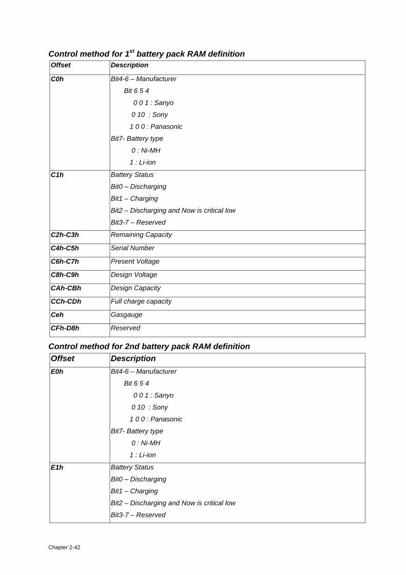
Control method for 1st battery pack RAM definition Offset Description
C0h Bit4-6 – Manufacturer
Bit 6 5 4
0 0 1 : Sanyo
0 10 : Sony
1 0 0 : Panasonic
Bit7- Battery type
0 : Ni-MH
1 : Li-ion
C1h Battery Status
Bit0 – Discharging
Bit1 – Charging
Bit2 – Discharging and Now is critical low
Bit3-7 – Reserved
C2h-C3h Remaining Capacity
C4h-C5h Serial Number
C6h-C7h Present Voltage
C8h-C9h Design Voltage
CAh-CBh Design Capacity
CCh-CDh Full charge capacity
Ceh Gasgauge
CFh-D8h Reserved
Control method for 2nd battery pack RAM definition Offset Description E0h Bit4-6 – Manufacturer
Bit 6 5 4
0 0 1 : Sanyo
0 10 : Sony
1 0 0 : Panasonic
Bit7- Battery type
0 : Ni-MH
1 : Li-ion
E1h Battery Status
Bit0 – Discharging
Bit1 – Charging
Bit2 – Discharging and Now is critical low
Bit3-7 – Reserved
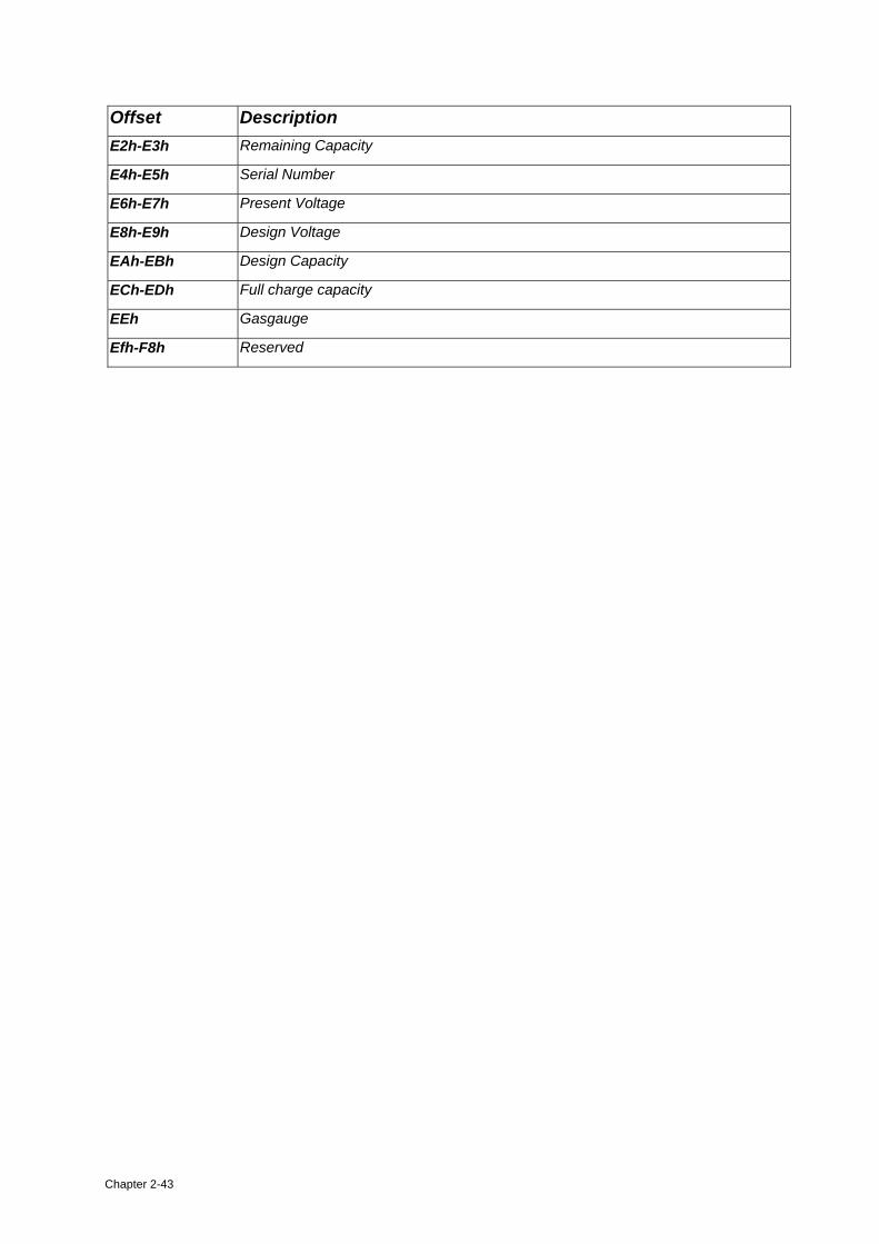
Chapter 2-43
Offset Description E2h-E3h Remaining Capacity
E4h-E5h Serial Number
E6h-E7h Present Voltage
E8h-E9h Design Voltage
EAh-EBh Design Capacity
ECh-EDh Full charge capacity
EEh Gasgauge
Efh-F8h Reserved
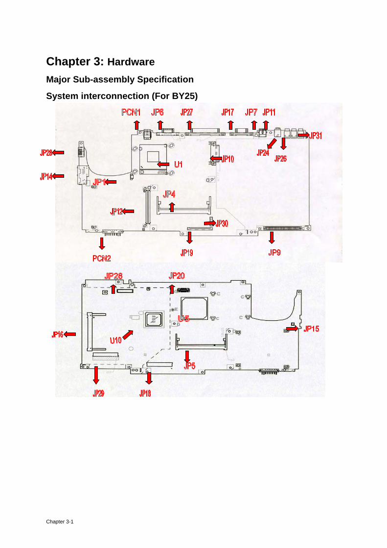
Chapter 3: Hardware Major Sub-assembly Specification
System interconnection (For BY25)
Chapter 3-1
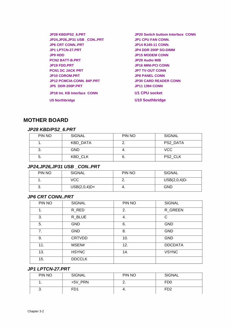
MOTHER BOARD JP28 KBD/PS2_6.PRT
PIN NO SIGNAL PIN NO SIGNAL
1. KBD_DATA 2. PS2_DATA
3. GND 4. VCC
5. KBD_CLK 6. PS2_CLK
JP24,JP26,JP31 USB _CON..PRT PIN NO SIGNAL PIN NO SIGNAL
1. VCC 2. USB(2,0,4)D-
3. USB(2,0,4)D+ 4. GND
JP6 CRT CONN..PRT PIN NO SIGNAL PIN NO SIGNAL
1. R_RED 2. R_GREEN
3. R_BLUE 4. C
5. GND 6. GND
7. GND 8. GND
9. CRTVDD 10. GND
11. MSEN# 12. DDCDATA
13. HSYNC 14. VSYNC
15. DDCCLK
JP1 LPTCN-27.PRT PIN NO SIGNAL PIN NO SIGNAL
1. +5V_PRN 2. FD0
3. FD1 4. FD2
JP28 KBD/PS2_6.PRT JP20 Switch buttom Interface CONNJP24,JP26,JP31 USB _CON..PRT JP1 CPU FAN CONN. JP6 CRT CONN..PRT JP14 RJ45-11 CONN. JP1 LPTCN-27.PRT JP4 DDR 200P SO-DIMM JP9 HDD JP15 MODEM CONN PCN2 BATT-B.PRT JP29 Audio M/B JP19 FDD.PRT JP16 MINI-PCI CONN PCN1 DC JACK PRT JP7 TV-OUT CONN JP10 CDROM.PRT JP8 PANEL CONN JP12 PCMCIA-CONN. 84P.PRT JP30 CARD READER CONN JP5 DDR-200P.PRT JP11 1394 CONN
JP18 Int. KB Interface CONN U1 CPU socket
U5 Northbridge U10 Southbridge
Chapter 3-2

5. FD3 6. FD4
7. FD5 8. FD6
9. FD7 10. LPTACK#
11. LPTBUSY 12. LPTPE
13. LPTSLCT 14. LPTAFD#
15. LPTERR# 16. LPT_INIT#
17. SLCTIN# 18. GND
19. GND 20. GND
21. GND 22. GND
23. GND 24. GND
25. GND
JP9 HDD PIN NO SIGNAL PIN NO SIGNAL
1. HD_IDERST# 2. GND
3. PD_D7 4. PD_D8
5. PD_D6 6. PD_D9
7. PD_D5 8. PD_D10
9. PD_D4 10. PD_D11
11. PD_D3 12. PD_D12
13. PD_D2 14. PD_D13
15. PD_D1 16. PD_D14
17. PD_D0 18. PD_D15
19. GND 20. NC
21. PD_DREQ 22. NC
23 PD_IOW# 24. GND
25. PD_IOR# 26. GND
27. PD_IORDY 28. PD_CSEL
29. PD_DACK# 30. GND
31. PD_IRQA 32. NC
33. PD_A1 34. CBLIDA
35. PD_A0 36. PD_A2
37. PD_CS#1 38. PD_CS#3
39. HDD_LED# 40. GND
41. +5VS 42. +5VS
43. GND 44. +5VS
PCN2 BATT-B.PRT PIN NO SIGNAL PIN NO SIGNAL
1. BATT+ 2. LI/NIMH#
Chapter 3-3

3. GND 4. BATT_TEMP
5. EEPROMVCC 6. SMB_EC_CK1
7. SMB_EC_DA1 8 GND
JP19 FDD.PRT PIN NO SIGNAL PIN NO SIGNAL
1. HDSEL# 2 GND
3 RDATA# 4 GND
5 WR# 6 GND
7 TRACK0# 8 GND
9 WGATE# 10 GND
11 WDATA# 12. FDD_DET#
13. STEP# 14. 3MODE
15 FDDIR# 16. NC
17 MTR0# 18. NC
19 NC 20. NC
21 DISKCHG# 22. +5VS
23 DRV0# 24. +5VS
25. INDEX# 26. +5VS
PCN1 DC JACK PRT (70W) PIN NO SIGNAL PIN NO SIGNAL
1. VIN 2. GND
JP10 CDROM.PRT PIN NO SIGNAL PIN NO SIGNAL
1. INT_CD_L 2. INT_CD_R
3. CD_AGND 4. GND
5. CD_IDERST# 6. SD_D8
7 SD_D7 8. SD_D9
9. SD_D6 10. SD_D10
11. SD_D5 12. SD_D11
13. SD_D4 14. SD_D12
15. SD_D3 16. SD_D13
17. SD_D2 18. SD_D14
19. SD_D1 20. SD_D15
21. SD_D0 22. SD_DREQ
23. GND 24. SD_SIOR#
25. SD_SIOW# 26. GND
27. SD_SIORDY 28. SD_DACK#
Chapter 3-4

29. SD_IRQ15 30. NC
31. SD_SBA1 32. CBLIDB
33. SD_SBA0 34. SD_SBA2
35. SD_CS1# 36. SD_SCS3#
37. CDLED# 38. +5V_IDE
39. +5V_IDE 40. +5V_IDE
41. +5V_IDE 42. +5V_IDE
43. GND 44. +5VS
45. GND 46. GND
47. SD_CSEL 48. GND
49. NC 50. +5VS
JP12 PCMCIA-CONN. 84P.PRT PIN NO SIGNAL PIN NO SIGNAL
A1. GND A2. GND
A3. S1_D3 A4. S1_CD1#
A5. S1_D4 A6. S1_D11
A7 S1_D5 A8. S1_D12
A9. GND A10. S1_D6
A11. S1_D13 A12. S1_D7
A13. S1_D14 A14. S1_CE1#
A15. S1_D15 A16. GND
A17. S1_A10 A18. S1_CE2#
A19. S1_OE# A20. S1_VS1
A21. S1_A11 A22. GND
A23. S1_IORD# A24. S1_A9
A25. S1_IOWR# A26. S1_A8
A27 S1_A17 A28 GND
A29. S1_A13 A30. S1_A18
A31. S1_A14 A32. S1_A19
A33. S1_WE# A34. S1_A20
A35. S1_RDY# A36. S1_A21
A37 S1_VCC A38 S1_VCC
A39. S1_VPP A40. S1_VPP
A41. S1_A16 A42. GND
A43. S1_A22 A44. S1_A15
A45. S1_A23 A46. S1_A12
A47. S1_A24 A48. S1_A7
A49. GND A50. S1_A25
Chapter 3-5
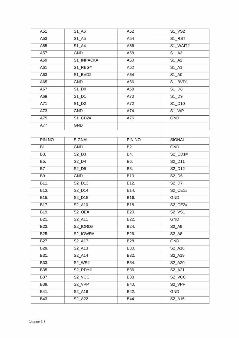
A51 S1_A6 A52 S1_VS2
A53 S1_A5 A54 S1_RST
A55 S1_A4 A56 S1_WAIT#
A57 GND A58 S1_A3
A59 S1_INPACK# A60 S1_A2
A61 S1_REG# A62 S1_A1
A63 S1_BVD2 A64 S1_A0
A65 GND A66 S1_BVD1
A67 S1_D0 A68 S1_D8
A69 S1_D1 A70 S1_D9
A71 S1_D2 A72 S1_D10
A73 GND A74 S1_WP
A75 S1_CD2# A76 GND
A77 GND
PIN NO SIGNAL PIN NO SIGNAL
B1. GND B2. GND
B3. S2_D3 B4. S2_CD1#
B5. S2_D4 B6. S2_D11
B7 S2_D5 B8. S2_D12
B9. GND B10. S2_D6
B11. S2_D13 B12. S2_D7
B13. S2_D14 B14. S2_CE1#
B15. S2_D15 B16. GND
B17. S2_A10 B18. S2_CE2#
B19. S2_OE# B20. S2_VS1
B21. S2_A11 B22. GND
B23. S2_IORD# B24. S2_A9
B25. S2_IOWR# B26. S2_A8
B27 S2_A17 B28 GND
B29. S2_A13 B30. S2_A18
B31. S2_A14 B32. S2_A19
B33. S2_WE# B34. S2_A20
B35. S2_RDY# B36. S2_A21
B37 S2_VCC B38 S2_VCC
B39. S2_VPP B40. S2_VPP
B41. S2_A16 B42. GND
B43. S2_A22 B44. S2_A15
Chapter 3-6
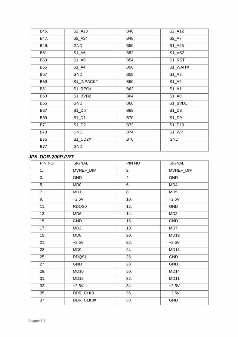
B45. S2_A23 B46. S2_A12
B47. S2_A24 B48. S2_A7
B49. GND B50. S1_A25
B51 S1_A6 B52 S1_VS2
B53 S1_A5 B54 S1_RST
B55 S1_A4 B56 S1_WAIT#
B57 GND B58 S1_A3
B59 S1_INPACK# B60 S1_A2
B61 S1_REG# B62 S1_A1
B63 S1_BVD2 B64 S1_A0
B65 GND B66 S1_BVD1
B67 S1_D0 B68 S1_D8
B69 S1_D1 B70 S1_D9
B71 S1_D2 B72 S1_D10
B73 GND B74 S1_WP
B75 S1_CD2# B76 GND
B77 GND
JP5 DDR-200P.PRT PIN NO SIGNAL PIN NO SIGNAL
1. MVREF_DIM 2. MVREF_DIM
3. GND 4. GND
5. MD0 6. MD4
7 MD1 8. MD5
9. +2.5V 10. +2.5V
11. RDQS0 12. GND
13. MD6 14. MD3
15. GND 16. GND
17. MD2 18. MD7
19. MD8 20. MD12
21. +2.5V 22. +2.5V
23. MD9 24. MD13
25. RDQS1 26. GND
27 GND 28 GND
29. MD10 30. MD14
31. MD15 32. MD11
33. +2.5V 34. +2.5V
35. DDR_CLK0 36. +2.5V
37 DDR_CLK0# 38 GND
Chapter 3-7

39. GND 40. GND
41. MD16 42. MD20
43. MD21 44. MD17
45. +2.5V 46. +2.5V
47. RDQS2 48. GND
49. MD18 50. MD22
51 GND 52 GND
53 MD19 54 MD23
55 MD24 56 MD28
57 +2.5V 58 +2.5V
59 MD25 60 MD29
61 RDQS3 62 GND
63 GND 64 GND
65 MD30 66 MD26
67 MD31 68 MD27
69 +2.5V 70 +2.5V
71 GND 72 GND
73 GND 74 GND
75 GND 76 GND
77 RDQS8 78 GND
79 GND 80 GND
81 +2.5V 82 +2.5V
83 GND 84 GND
85 NC 86 NC
87 GND 88 GND
89 DDRCLK2 90 GND
91 DDRCLK2# 92 +2.5V
93 +2.5V 94 +2.5V
95 CKE3 96 CKE2
97 GND 98 GND
99 MAA12 100 MAA11
101 MAA9 102 MAA8
103 GND 104 GND
105 MAA7 106 MAA6
107 MAA5 108 MAA4
109 MAA3 110 MAA2
111 MAA1 112 MAA0
113 +2.5V 114 +2.5V
Chapter 3-8

115 MAA10 116 MAA12
117 MAA11 118 SRAS#
119 SWE# 120 SCAS#
121 RCS0# 122 RCS1#
123 NC 124 NC
125 GND 126 GND
127 MD32 128 MD36
129 MD37 130 MD33
131 +2.5V 132 +2.5V
133 RDQS4 134 GND
135 MD34 136 MD38
137 GND 138 GND
139 MD35 140 MD39
141 MD40 142 MD44
143 +2.5V 144 +2.5V
145 MD41 146 MD45
147 RDQS5 148 GND
149 GND 150 GND
151 MD42 152 MD43
153 MD46 154 MD47
155 +2.5V 156 +2.5V
157 +2.5V 158 DDR_CLK1#
159 GND 160 DDR_CLK1
161 GND 162 GND
163 MD48 164 MD49
165 MD52 166 MD53
167 +2.5V 168 +2.5V
169 RDQS6 170 GND
171 MD50 172 MD54
173 GND 174 GND
175 MD51 176 MD55
177 MD57 178 MD56
179 +2.5V 180 +2.5V
181 MD61 182 MD60
183 RDQS7 184 GND
185 GND 186 GND
187 MD58 188 MD62
189 MD59 190 MD63
Chapter 3-9

191 +2.5V 192 +2.5V
193 SMBDAT 194 GND
195 SMBCK 196 GND
197 +3VS 198 GND
199 NC 200 NC
JP18 Int. KB Interface CONN PIN NO SIGNAL PIN NO SIGNAL
1. ID1 2. ID2 3. GND 4. USER BTN# 5. LED+ 6. LED- 7 KSO0 8. KSO1 9. KSO2 10. KSO3 11. KSO4 12. KSO5 13. KSO6 14. KSO7 15. KSO8 16. KSO9 17. KSO10 18. KSO11 19. KSO12 20. KSO13 21. KSO14 22. KSO15 23. KSI0 24. KSI1 25. KSI2 26. KSI3 27 KSI4 28 KSI5 29. KSI6 30. KSI7
JP20 Switch buttom Interface CONN PIN NO SIGNAL PIN NO SIGNAL
1. +3VALW 2. +3VS 3. SCROLLLED# 4. NUMLED# 5. CAPSLED# 6. 51ON# 7 EC ACT# 8. GND-MIC 9. INT MIC 10. GND-MIC 11. USER BTN0# 12. USER BTN1# 13. USER BTN2# 14. USER BTN3# 15. GND 16. NC 17. NC 18. NC 19. NC 20. GND
JP1 CPU FAN CONN. PIN NO SIGNAL PIN NO SIGNAL
1. +5VFAN1 2. FAN1_SPEED1 3. GND
Chapter 3-10
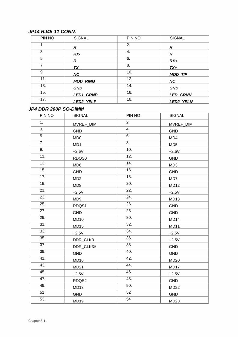
JP14 RJ45-11 CONN. PIN NO SIGNAL PIN NO SIGNAL
1. R 2. R 3. RX- 4. R 5. R 6. RX+ 7 TX- 8. TX+ 9. NC 10. MOD TIP 11. MOD RING 12. NC 13. GND 14. GND 15. LED1 GRNP 16. LED GRNN 17. LED2 YELP 18. LED2 YELN
JP4 DDR 200P SO-DIMM PIN NO SIGNAL PIN NO SIGNAL
1. MVREF_DIM 2. MVREF_DIM 3. GND 4. GND 5. MD0 6. MD4 7 MD1 8. MD5 9. +2.5V 10. +2.5V 11. RDQS0 12. GND 13. MD6 14. MD3 15. GND 16. GND 17. MD2 18. MD7 19. MD8 20. MD12 21. +2.5V 22. +2.5V 23. MD9 24. MD13 25. RDQS1 26. GND 27 GND 28 GND 29. MD10 30. MD14 31. MD15 32. MD11 33. +2.5V 34. +2.5V 35. DDR_CLK3 36. +2.5V 37 DDR_CLK3# 38 GND 39. GND 40. GND 41. MD16 42. MD20 43. MD21 44. MD17 45. +2.5V 46. +2.5V 47. RDQS2 48. GND 49. MD18 50. MD22 51 GND 52 GND 53 MD19 54 MD23
Chapter 3-11

55 MD24 56 MD28 57 +2.5V 58 +2.5V 59 MD25 60 MD29 61 RDQS3 62 GND 63 GND 64 GND 65 MD30 66 MD26 67 MD31 68 MD27 69 +2.5V 70 +2.5V 71 GND 72 GND 73 GND 74 GND 75 GND 76 GND 77 RDQS8 78 GND 79 GND 80 GND 81 +2.5V 82 +2.5V 83 GND 84 GND 85 NC 86 NC 87 GND 88 GND 89 DDRCLK5 90 GND 91 DDRCLK5# 92 +2.5V 93 +2.5V 94 +2.5V 95 CKE3 96 CKE2 97 GND 98 GND 99 MAA12 100 MAA11 101 MAA9 102 MAA8 103 GND 104 GND 105 MAA7 106 MAA6 107 MAA5 108 MAA4 109 MAA3 110 MAA2 111 MAA1 112 MAA0 113 +2.5V 114 +2.5V 115 MAA10 116 MAA12 117 MAA11 118 SRAS# 119 SWE# 120 SCAS# 121 RCS2# 122 RCS3# 123 NC 124 NC 125 GND 126 GND 127 MD32 128 MD36 129 MD37 130 MD33 131 +2.5V 132 +2.5V 133 RDQS4 134 GND 135 MD34 136 MD38
Chapter 3-12
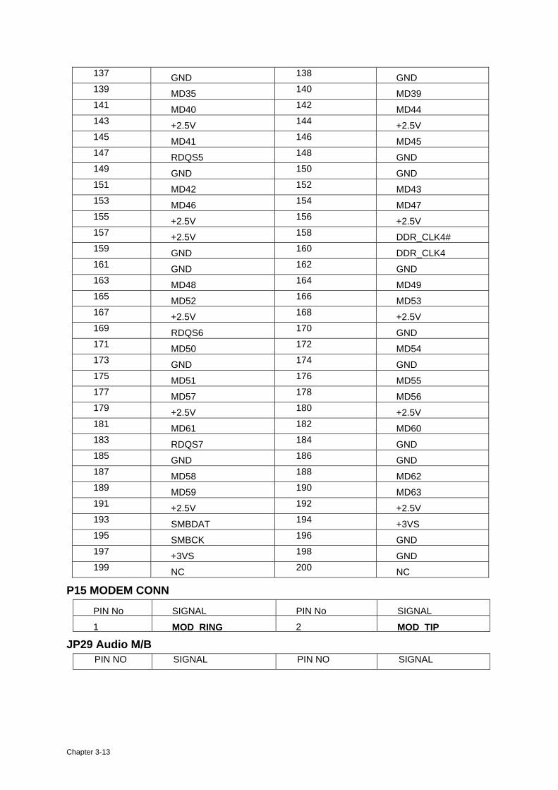
137 GND 138 GND 139 MD35 140 MD39 141 MD40 142 MD44 143 +2.5V 144 +2.5V 145 MD41 146 MD45 147 RDQS5 148 GND 149 GND 150 GND 151 MD42 152 MD43 153 MD46 154 MD47 155 +2.5V 156 +2.5V 157 +2.5V 158 DDR_CLK4# 159 GND 160 DDR_CLK4 161 GND 162 GND 163 MD48 164 MD49 165 MD52 166 MD53 167 +2.5V 168 +2.5V 169 RDQS6 170 GND 171 MD50 172 MD54 173 GND 174 GND 175 MD51 176 MD55 177 MD57 178 MD56 179 +2.5V 180 +2.5V 181 MD61 182 MD60 183 RDQS7 184 GND 185 GND 186 GND 187 MD58 188 MD62 189 MD59 190 MD63 191 +2.5V 192 +2.5V 193 SMBDAT 194 +3VS 195 SMBCK 196 GND 197 +3VS 198 GND 199 NC 200 NC
P15 MODEM CONN
PIN No SIGNAL PIN No SIGNAL
1 MOD RING 2 MOD TIP
JP29 Audio M/B PIN NO SIGNAL PIN NO SIGNAL
Chapter 3-13
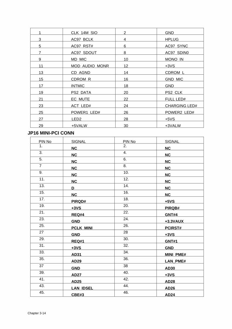
1 CLK 14M SIO 2 GND
3 AC97 BCLK 4 HPLUG
5 AC97 RST# 6 AC97 SYNC
7 AC97 SDOUT 8 AC97 SDIN0
9 MD MIC 10 MONO IN
11 MOD AUDIO MONR 12 +3VS
13 CD AGND 14 CDROM L
15 CDROM R 16 GND MIC
17 INTMIC 18 GND
19 PS2 DATA 20 PS2 CLK
21 EC MUTE 22 FULL LED#
23 ACT LED# 24 CHARGING LED#
25 POWER1 LED# 26 POWER2 LED#
27 LED2 28 +5VS
29 +5VALW 30 +3VALW
JP16 MINI-PCI CONN
PIN No SIGNAL PIN No SIGNAL 1. NC 2. NC 3. NC 4. NC 5. NC 6. NC 7 NC 8. NC 9. NC 10. NC 11. NC 12. NC 13. D 14. NC 15. NC 16. NC 17. PIRQD# 18. +5VS 19. +3VS 20. PIRQB# 21. REQ#4 22. GNT#4 23. GND 24. +3.3VAUX 25. PCLK MINI 26. PCIRST# 27 GND 28 +3VS 29. REQ#1 30. GNT#1 31. +3VS 32. GND 33. AD31 34. MINI PME# 35. AD29 36. LAN_PME# 37 GND 38 AD30 39. AD27 40. +3VS 41. AD25 42. AD28 43. LAN IDSEL 44. AD26 45. CBE#3 46. AD24
Chapter 3-14
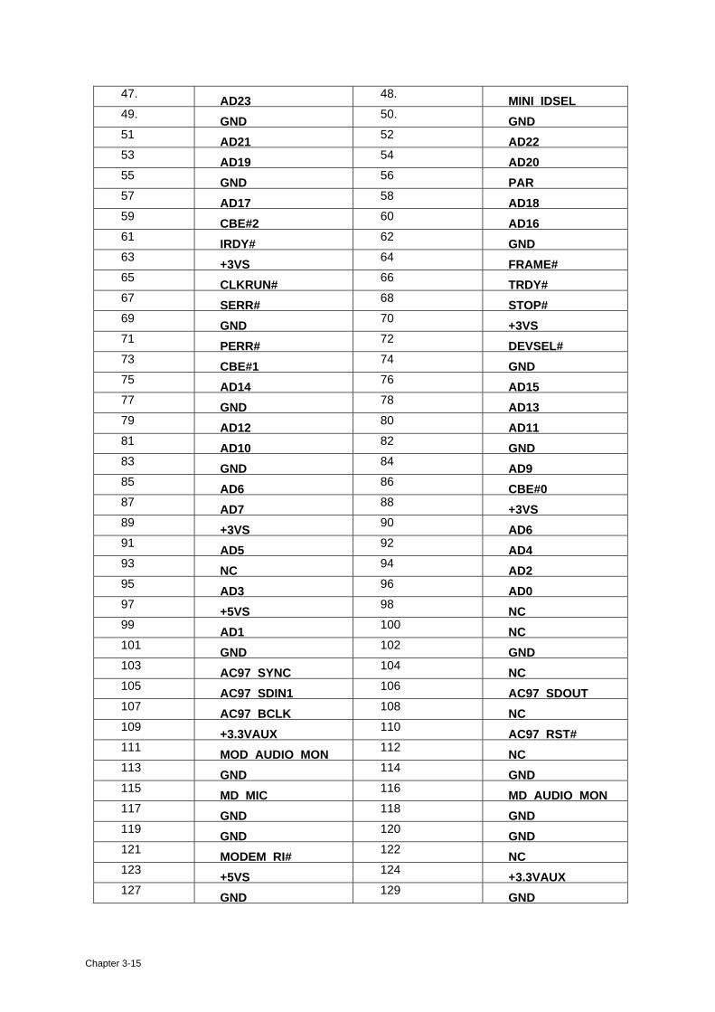
47. AD23 48. MINI IDSEL 49. GND 50. GND 51 AD21 52 AD22 53 AD19 54 AD20 55 GND 56 PAR 57 AD17 58 AD18 59 CBE#2 60 AD16 61 IRDY# 62 GND 63 +3VS 64 FRAME# 65 CLKRUN# 66 TRDY# 67 SERR# 68 STOP# 69 GND 70 +3VS 71 PERR# 72 DEVSEL# 73 CBE#1 74 GND 75 AD14 76 AD15 77 GND 78 AD13 79 AD12 80 AD11 81 AD10 82 GND 83 GND 84 AD9 85 AD6 86 CBE#0 87 AD7 88 +3VS 89 +3VS 90 AD6 91 AD5 92 AD4 93 NC 94 AD2 95 AD3 96 AD0 97 +5VS 98 NC 99 AD1 100 NC 101 GND 102 GND 103 AC97 SYNC 104 NC 105 AC97 SDIN1 106 AC97 SDOUT 107 AC97 BCLK 108 NC 109 +3.3VAUX 110 AC97 RST# 111 MOD AUDIO MON 112 NC 113 GND 114 GND 115 MD MIC 116 MD AUDIO MON117 GND 118 GND 119 GND 120 GND 121 MODEM RI# 122 NC 123 +5VS 124 +3.3VAUX 127 GND 129 GND
Chapter 3-15

JP7 TV-OUT CONN
PIN No SIGNAL PIN No SIGNAL 1 GND 2 LUMA 3 GND 4 CRMA 5 GND 67 COMPS
JP8 PANEL CONN
PIN No SIGNAL PIN No SIGNAL 1. LCDVDD 2. LCDVDD 3. DC2 4. GND 5. TX0- 6. TX0+ 7 GND 8. TX1- 9. TX1+ 10. GND 11. TX4- 12. TX4+ 13. GND 14. TXBCLK- 15. TXBCLK+ 16. GND 17. PID3 18. PID2 19. PID1 20. PID0 21. TX2- 22. TX2+ 23. GND 24. TCACLK- 25. TXACLK+ 26. GND 27 TX5- 28 TX5+ 29. GND 30. TX6- 31. TX6+ 32. GND 33. DD2 34. LCDVDD 35. LCDVDD 36. DAC BRIG 37 INVT PWM 38 DISPOFF# 39. B+ 40. B+
JP30 CARD READER CONN
PIN No SIGNAL PIN No SIGNAL 1 +5VS 2 +5VS 3 USB5 D+ 4 USB5 D- 5 PCIRST# 6 GND
JP11 1394 CONN
PIN No SIGNAL PIN No SIGNAL 1 XTPA0+ 2 XTPA0- 3 XTPB0+ 4 XTPB0-
Chapter 3-16

Chapter 4: AC-DC CONVERTER ACY25 series Power System block diagram
Chapter 4-1
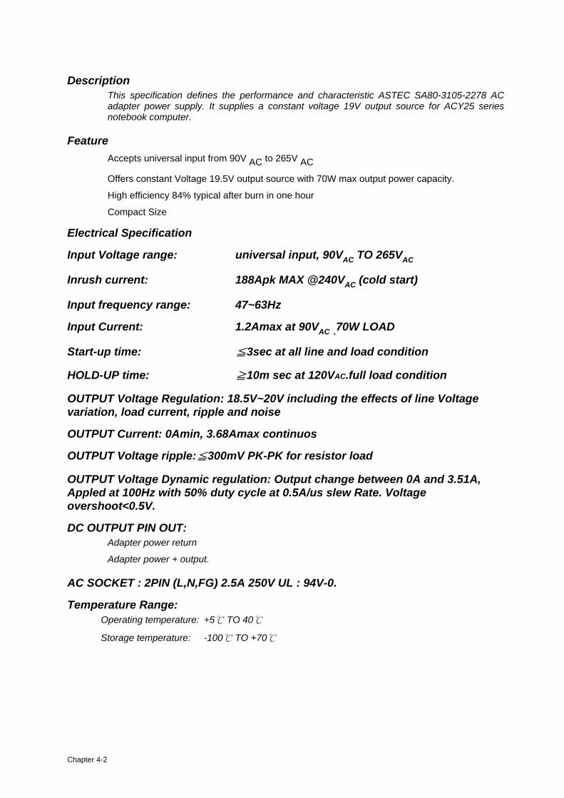
Description This specification defines the performance and characteristic ASTEC SA80-3105-2278 AC adapter power supply. It supplies a constant voltage 19V output source for ACY25 series notebook computer.
Feature Accepts universal input from 90V AC to 265V AC
Offers constant Voltage 19.5V output source with 70W max output power capacity.
High efficiency 84% typical after burn in one hour
Compact Size
Electrical Specification
Input Voltage range: universal input, 90VAC TO 265VAC
Inrush current: 188Apk MAX @240VAC (cold start)
Input frequency range: 47~63Hz
Input Current: 1.2Amax at 90VAC ,70W LOAD
Start-up time: ≦3sec at all line and load condition
HOLD-UP time: ≧10m sec at 120VAC.full load condition
OUTPUT Voltage Regulation: 18.5V~20V including the effects of line Voltage variation, load current, ripple and noise
OUTPUT Current: 0Amin, 3.68Amax continuos
OUTPUT Voltage ripple:≦300mV PK-PK for resistor load
OUTPUT Voltage Dynamic regulation: Output change between 0A and 3.51A, Appled at 100Hz with 50% duty cycle at 0.5A/us slew Rate. Voltage overshoot<0.5V.
DC OUTPUT PIN OUT: Adapter power return
Adapter power + output.
AC SOCKET : 2PIN (L,N,FG) 2.5A 250V UL : 94V-0.
Temperature Range: Operating temperature: +5℃ TO 40℃
Storage temperature: -100℃ TO +70℃
Chapter 4-2

DC-DC CONVERTER Description
The DC-DC converter is designed to supply the power for ACY25 series notebook computer of Compal. It supply +5VALWP, +3VALWP, +1.8VALWP, +2.5VP, +CPU_CORE, +1.25VP,+1.2VP for logical system, and supplies for the built-in NS87591 microprocessor which handles the keyboard and PMU control functions of the system. The power ON/OFF is also controlled by NS87591.There is also a charger power source built-in it. It can charge battery pack whether the computer is ON or OFF.
Features
High efficiency, up to 90%(using battery)
Accept wide range DC input voltage from 8V to 21V
Built-in charger power source
The power ON/OFF is controlled by software
Electrical specification
Input Voltage/Current
10V to 20V at the summing point of AC Adapter and battery
INPUT Current 5A max from battery
INPUT Current 3.5A max from AC Adapter
Temperature Range:
Operating temperature : 0℃ to 40℃
storage temperature range : -20℃ to 65℃
Chapter 4-3
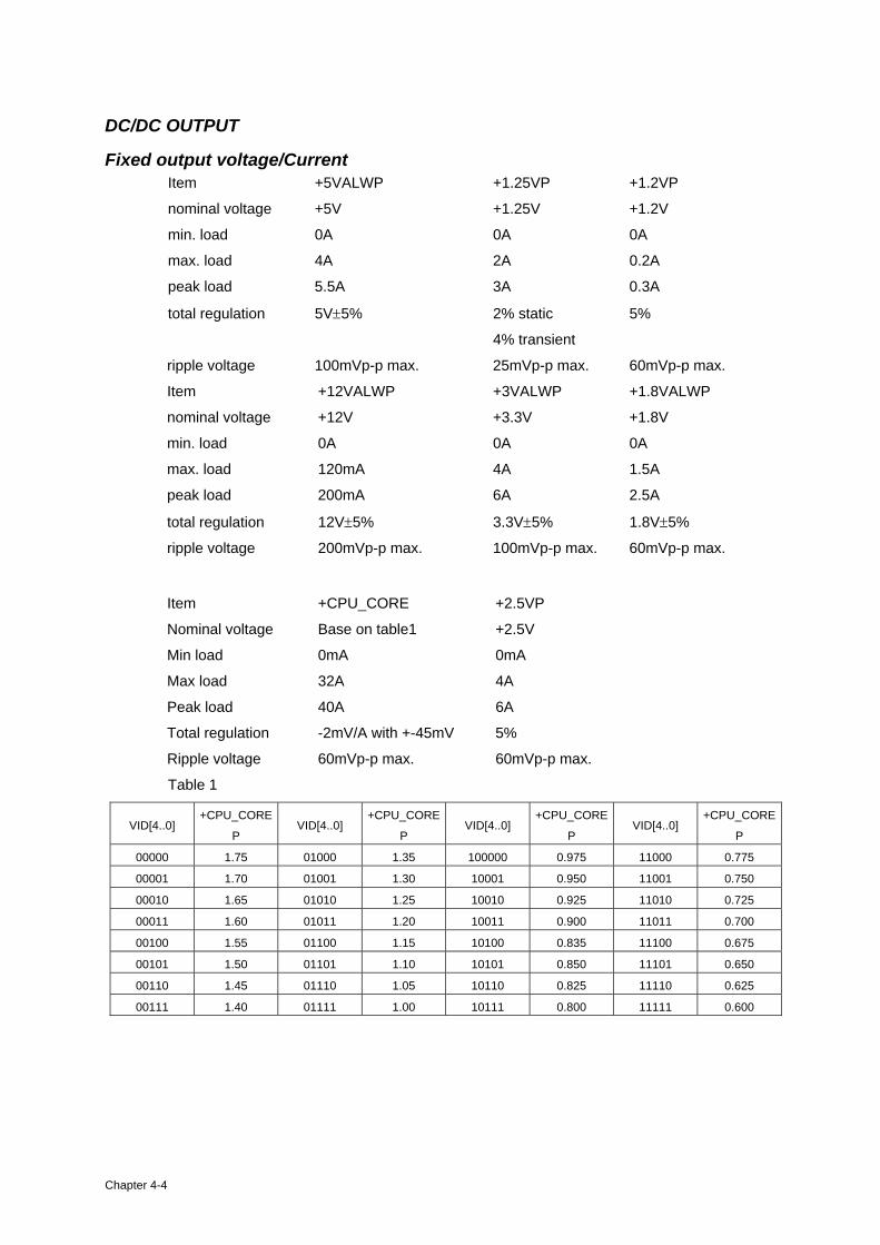
DC/DC OUTPUT
Fixed output voltage/Current Item +5VALWP +1.25VP +1.2VP
nominal voltage +5V +1.25V +1.2V
min. load 0A 0A 0A
max. load 4A 2A 0.2A
peak load 5.5A 3A 0.3A
total regulation 5V±5% 2% static 5%
4% transient
ripple voltage 100mVp-p max. 25mVp-p max. 60mVp-p max.
Item +12VALWP +3VALWP +1.8VALWP
nominal voltage +12V +3.3V +1.8V
min. load 0A 0A 0A
max. load 120mA 4A 1.5A
peak load 200mA 6A 2.5A
total regulation 12V±5% 3.3V±5% 1.8V±5%
ripple voltage 200mVp-p max. 100mVp-p max. 60mVp-p max.
Item +CPU_CORE +2.5VP
Nominal voltage Base on table1 +2.5V
Min load 0mA 0mA
Max load 32A 4A
Peak load 40A 6A
Total regulation -2mV/A with +-45mV 5%
Ripple voltage 60mVp-p max. 60mVp-p max.
Table 1
VID[4..0] +CPU_CORE
P VID[4..0]
+CPU_CORE
P VID[4..0]
+CPU_CORE
P VID[4..0]
+CPU_CORE
P
00000 1.75 01000 1.35 100000 0.975 11000 0.775
00001 1.70 01001 1.30 10001 0.950 11001 0.750
00010 1.65 01010 1.25 10010 0.925 11010 0.725
00011 1.60 01011 1.20 10011 0.900 11011 0.700
00100 1.55 01100 1.15 10100 0.835 11100 0.675
00101 1.50 01101 1.10 10101 0.850 11101 0.650
00110 1.45 01110 1.05 10110 0.825 11110 0.625
00111 1.40 01111 1.00 10111 0.800 11111 0.600
Chapter 4-4
Charger
Controlled by NS87591 microprocessor from motherboard
Temperature sense capability for the battery (charge active between 0℃~ 40℃)
fast charge [2.5Amps-8cells(3900mAH), LiIon Battery when system off, approach 30W fast charge when system ON.(depend on system load)
Charging termination: check the Full_charged bit in Battery status of Smart Battery.
When system turns off, the charging time from empty to full is 3.0 hrs typically at room temperature.
Other battery services are presented by NS87591 microprocessor include maximum charging timer, charging temperature range etc.
Charger power:
BATT++ Constant voltage mode: 16.8V±1%
Constant charger current mode:2.5A±10%-8cells(3900mAH)
Constant adapter current mode:3.20A±10%
OVER Current protection: +5VALWP: 5.67~9.17A +3.3VALWP: 5.23~8.73A +CPU_CORE: 40~60A
OVER Voltage protection: +5VALWP: V0+V0*(4~10%) +3.3VALWP: V0+V0*(4~10%) +CPU_CORE: V0+V0*12%
Short circuit protection: latch mode for +5VALWP, +3VALWP, +CPU_CORE auto recovery mode for +12VALWP
I/O
P1:Ac adapter input Jack socket Pin 1: Adapter power return
Pin 2: Adapter power + input
Chapter 4-5
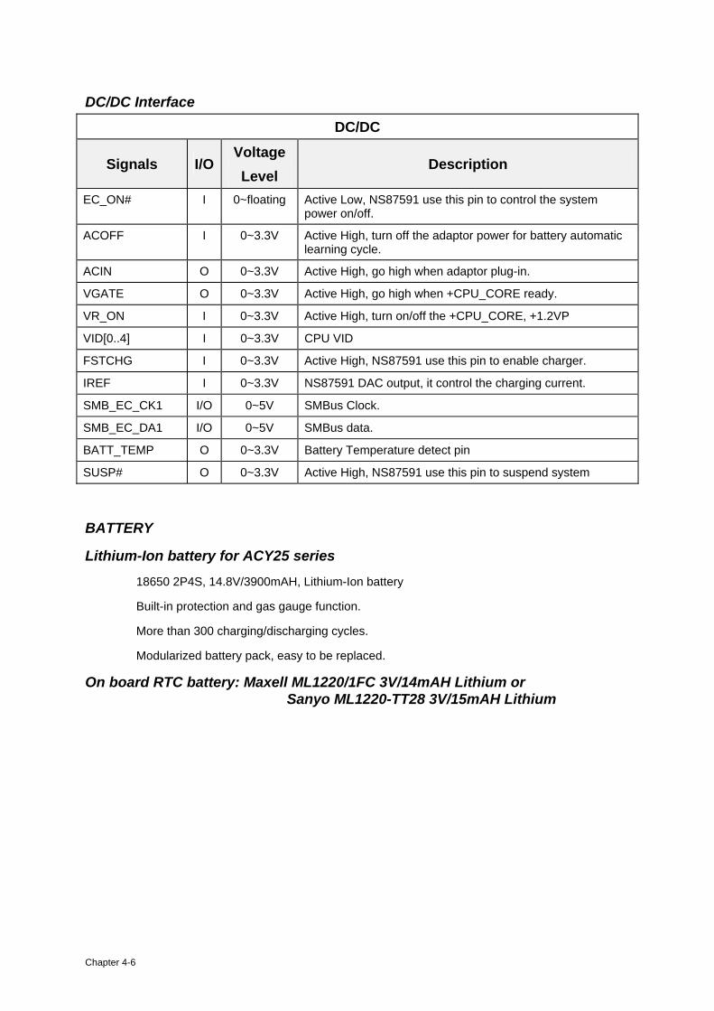
DC/DC Interface
DC/DC
Signals I/OVoltage Level
Description
EC_ON# I 0~floating Active Low, NS87591 use this pin to control the system power on/off.
ACOFF I 0~3.3V Active High, turn off the adaptor power for battery automatic learning cycle.
ACIN O 0~3.3V Active High, go high when adaptor plug-in.
VGATE O 0~3.3V Active High, go high when +CPU_CORE ready.
VR_ON I 0~3.3V Active High, turn on/off the +CPU_CORE, +1.2VP
VID[0..4] I 0~3.3V CPU VID
FSTCHG I 0~3.3V Active High, NS87591 use this pin to enable charger.
IREF I 0~3.3V NS87591 DAC output, it control the charging current.
SMB_EC_CK1 I/O 0~5V SMBus Clock.
SMB_EC_DA1 I/O 0~5V SMBus data.
BATT_TEMP O 0~3.3V Battery Temperature detect pin
SUSP# O 0~3.3V Active High, NS87591 use this pin to suspend system
BATTERY
Lithium-Ion battery for ACY25 series
18650 2P4S, 14.8V/3900mAH, Lithium-Ion battery
Built-in protection and gas gauge function.
More than 300 charging/discharging cycles.
Modularized battery pack, easy to be replaced.
On board RTC battery: Maxell ML1220/1FC 3V/14mAH Lithium or Sanyo ML1220-TT28 3V/15mAH Lithium
Chapter 4-6
ACY25 14.1” & 15” INVERTER SPECIFICATION General Description
There are two control signals that come from system to control lamp brightness. One signal is named DAC_BRIG, which limits current to meet LCD lamp current specification. Another one is named PWM, which adjusts lamp brightness. This inverter brightness is adjusted by PWM burst mode. The PWM burst mode is that turning on and off the lamp at a rate of 150Hz. The effective brightness is a function of the duty cycle.
Features Wide range 9V to 21V input voltage
Brightness adjustment by PWM burst mode.
Close loop controls lamp current.
Absolute maximum rating
Environment: Temperature: Operating temperature: 0℃ ~ 55℃
Storage temperature : -20℃ ~ 70℃
Humidity: 0 ~ 90% without condensation
MTBF: 50000 hours.
Electrical characteristic
No Item Symbol Min. Typ. Max. Unit Comment
1 Input voltage INV_PWR 9 14.8 21 V
2 Input current Iin -- 0.33 -- A
3 Lamp current IL 2.7 -- 6.3 mA *Note 1
4 Frequency F 45 55 65 KHz *Note2
5 Output power Pout -- -- 4.5 W
6 Efficiency η 80% -- -- --
7 Starting voltage Vs 1600 -- -- V At 0’C
8 Starting time Tvs 1 -- 1.5 Sec
2.8 3.3 3.6 V Backlight on/off signal 9 Dispoff#
0 0.5 0.8 V Low level
10 Limited lamp maximum current DAC-BRIG 0 3.3 V *Note 1
Chapter 4-7
142 150 158 Hz PWM signal frequency
3.0 3.3 3.6 V PWM signal amplitude 11 PWM signal *note 4 INV_PWM
30 -- 100 % Period
TonDuty =
12 lamp current over-shoot PKZeroI − -- -- 10 %
Line transient( 10.8V to 21V/100us) and turn on transient
13 Current Waveform factor
rms
p
II
1.27 2 1.56 Multiple OR rms
p
II− *10
14 Unbalance
Rate rms
pp
I
II −− -10% 0 +10% Multiple
15 Turn off voltage Voff -- -- 100Vp-p V PWM=40%
16 Voltage Rise time Trise -- -- 300us us PWM=40%
17 Voltage fall time Tfall -- -- 300us us PWM=40%
Notes:
*1. Limited lamp maximum current by DAC_BRIG signal:
When DAC_BRIG voltage is 0V and INV_PWM enables (100%), lamp has max. limited current.
When DAC_BRIG voltage is 3.3V and INV_PWM enables (100%), lamp has min. limited current.
DAC_BRIG signal comes from system chipset with internal resistance of 3KΩ.
*2. Inverter operating frequency should be within specification (45~65kHz) at max. and min. brightness load.
*3. INV_PWM enable implies INV_PWM signal is High level (On duty cycle is 100%). It is a square wave of 150Hz to adjust backlight brightness that is a function of PWM duty cycle. Backlight brightness is maximum value under INV_PWM at 100% and brightness is minimum under INV_PWM at 40%.
*4. The system interface signals belong to 3.3V.
*5. Please make sure open lamp output voltage should be within starting voltage specification.
*6. Inverter should pass human body safety test.
*7. Inverter should no smoking by any component open/ short test
*8. Transformer voltage stress should not be over 85% under any condition
( turn on overshoot transient and line transient).
*9. Audio noise should be less than 36dB at 10 cm distance.
Chapter 4-8
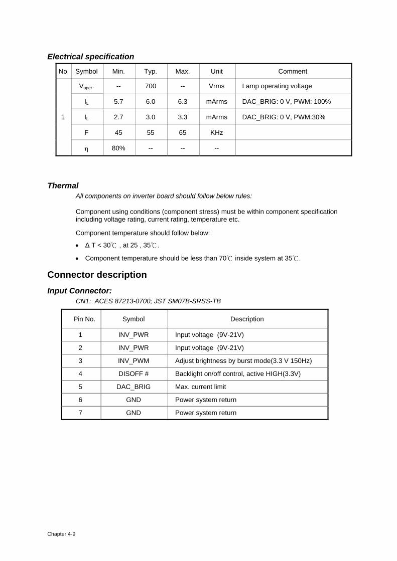
Electrical specification
No Symbol Min. Typ. Max. Unit Comment
Voper. -- 700 -- Vrms Lamp operating voltage
IL 5.7 6.0 6.3 mArms DAC_BRIG: 0 V, PWM: 100%
IL 2.7 3.0 3.3 mArms DAC_BRIG: 0 V, PWM:30%
F 45 55 65 KHz
1
η 80% -- -- --
Thermal
All components on inverter board should follow below rules:
Component using conditions (component stress) must be within component specification including voltage rating, current rating, temperature etc.
Component temperature should follow below:
• Δ T < 30℃ , at 25 , 35℃.
• Component temperature should be less than 70℃ inside system at 35℃.
Connector description Input Connector:
CN1: ACES 87213-0700; JST SM07B-SRSS-TB
Pin No. Symbol Description
1 INV_PWR Input voltage (9V-21V)
2 INV_PWR Input voltage (9V-21V)
3 INV_PWM Adjust brightness by burst mode(3.3 V 150Hz)
4 DISOFF # Backlight on/off control, active HIGH(3.3V)
5 DAC_BRIG Max. current limit
6 GND Power system return
7 GND Power system return
Chapter 4-9

Output Connector: CN2: JST_SM02B_BHSS-1
Pin No. Symbol Description
1 HV Connected to high voltage of LCD lamp
2 LV Connected to low voltage of LCD lamp
Note : Please mark “ CAUTION HIGH VOLTAGE” around CN2
Safety Protection Open lamp protection:
When inverter is on open lamp status, any component on inverter should be O.K and inverter is no damaged, no fire and no arcing. If inverter can’t shunt down during open lamp happen, inverter must pass below conditions:
Human body test.
Open lamp burning: Inverter burns for 24 hours at open lamp status. No parts damage.
Human body safety test: Short inverter output, transformer secondary output to GND by a 2KΩ resistor which connects one end to GND and another one to those outputs. They should meet output current limitation requirement as follow. Output current I is the current that flows through 2KΩ resistor.
Output current I ≦ 0.7mA , if frequency f ≦ 1KHz
Output current I ≦ 0.7mA * f (kHz) , if f ≧ 1KHz. However, output current should be less than 70mA even frequency is more than 100KHz.
Abnormal test: Any one component is short or open; inverter should be no fire, no arcing. And result must meet output current limitation requirement.
Chapter 4-10
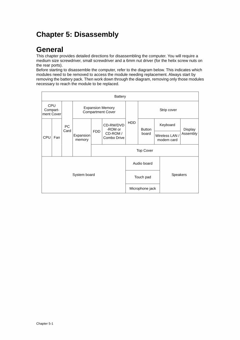
Chapter 5: Disassembly General This chapter provides detailed directions for disassembling the computer. You will require a medium size screwdriver, small screwdriver and a 6mm nut driver (for the helix screw nuts on the rear ports). Before starting to disassemble the computer, refer to the diagram below. This indicates which modules need to be removed to access the module needing replacement. Always start by removing the battery pack. Then work down through the diagram, removing only those modules necessary to reach the module to be replaced.
Battery
CPU Compart-
ment Cover
Expansion Memory Compartment Cover Strip cover
Keyboard
FDD
CD-RW/DVD-ROM or
CD-ROM / Combo Drive
HDD
Button board Wireless LAN /
modem card
Display Assembly
CPU Fan
PC Card
Expansion memory
Top Cover
Audio board
Touch pad System board
Microphone jack
Speakers
Chapter 5-1
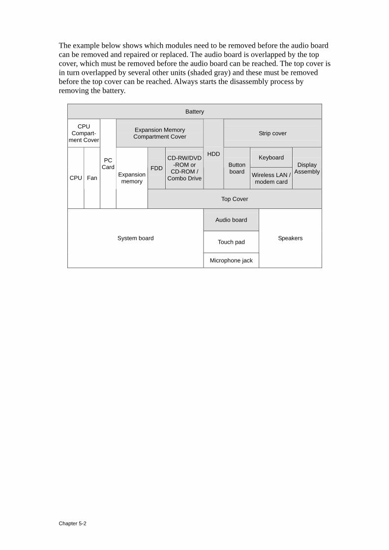
The example below shows which modules need to be removed before the audio board can be removed and repaired or replaced. The audio board is overlapped by the top cover, which must be removed before the audio board can be reached. The top cover is in turn overlapped by several other units (shaded gray) and these must be removed before the top cover can be reached. Always starts the disassembly process by removing the battery.
Battery
CPU Compart-
ment Cover
Expansion Memory Compartment Cover Strip cover
Keyboard
FDD
CD-RW/DVD-ROM or
CD-ROM / Combo Drive
HDD
Button board Wireless LAN /
modem card
Display Assembly
CPU Fan
PC Card
Expansion memory
Top Cover
Audio board
Touch pad System board
Microphone jack
Speakers
Chapter 5-2

Safety Precautions
Before you begin disassembly, read the following safety precautions and observe them carefully as you work.
DANGER: 1. Always use the lithium ion battery pack or backup battery that is authorized by the
manufacturer or compatible with the unit. Since other battery packs have different specifications, they may be incompatible with the unit, and may burst or explode. Heating or disassembling the battery pack could cause leakage of alkaline solution. Throwing the battery pack into a fire could cause the battery pack to explode.
2. The power supply, FL inverter and other components carry high voltages. To avoid the risk of electric shock when you need to turn on the power of a partially disassembled computer to check its operation, be very careful not to touch connectors or components. Also, do not disassemble individual components in first-level maintenance.
WARNING: To avoid the risk of electric shock or other injury: 1. Always turn the power off and disconnect the AC adaptor from the power source. 2. Remove any metal jewelry or accessories such as necklaces, bracelets, or rings. Batteries in the
computer retain an electrical charge so there is danger of electrical shock even when the computer is disconnected from an AC power source.
3. Never work with wet or damp hands. 4. The computer contains sharp edges and corners: be careful not to injure yourself. 5. Make sure that all replacement components meet the specifications for the computer and that all
cables and connectors are securely fastened.
CAUTION: To avoid damage to the computer: 1. When you change a component, be sure the replacement component meets the required
specifications. Never use foreign parts. 2. Metal objects such as screws or paper clips which fall into the unit can cause a short-circuit, fire,
or other internal damage. 3. When assembling the computer, make sure you use the correct screws to secure the various
pieces in place. Screw sizes are listed in their corresponding figure. Make sure all screws are securely fastened. Loose screws can cause short circuits, resulting in heat, smoke, or fire.
4. Before removing an module or other component, make sure all cables to the component have been disconnected.
5. If you use AC power, be sure to use the cable that came with the computer or one recommended by the manufacturer.
Chapter 5-3

Before You Begin
Look over the procedures in this section before you begin disassembling the computer. Familiarize yourself with the disassembly and reassembly steps. Begin each procedure by removing the AC adaptor and the battery pack.
1. Do not disassemble the computer unless it is operating abnormally.
2. Use only the correct and approved tools.
3. Make sure the working environment is free from the following elements whether you are using or storing the computer.
Dust and contaminates Static electricity Extreme heat, cold and humidity
4. Do not perform any operations that are not necessary and use only the described procedures for disassembling and installing modules in the computer.
5. After removing parts from the computer, place them in a safe place away from the computer so they will not be damaged and will not interfere with your work.
6. You will remove and replace many screws when you disassemble the computer. When you remove screws, make sure they are placed in a safe place and identified with the correct parts.
7. When assembling the computer make sure you use the correct screws to secure the various pieces. Screw sizes are listed in their corresponding figures.
8. The computer contains many sharp edges and corners, so be careful not to injure yourself.
9. After you have replaced a component, make sure the computer is functioning properly by performing the appropriate test on the component you have fixed or replaced.
Chapter 5-4

Disassembly Procedures
The computer has two basic types of cable connectors: Pressure Plate Connectors Standard Pin Connectors
To disconnect a Pressure Plate connector, lift up the tabs on either side of the connector’s plastic pressure plate and slide the cable out of the connector. To connect the cable to a Pressure Plate connector, make sure the pressure plate is fully lifted and slide the cable into the connector. Secure the cable in place by pushing the sides of the pressure plate down so the plate is flush with the sides of the connector. Gently pull on the cable to make sure the cable is secure. If you pull out the connector, connect it again making sure the connector’s pressure plate is fully lifted when you insert the cable. Standard pin connectors are used with all other cables. These connectors can be connected and disconnected by simply pulling them apart or pushing them together. Assembly Procedures
After you have disassembled the computer and fixed or repaired the problem that was causing the computer to operate abnormally, you will need to reassemble the computer. While assembling the computer, remember the following general points:
Take your time. Most problems arise when you get in a hurry assembling the computer.
Make sure all cables and connectors are securely fastened.
Before securing the module or other parts, make sure that no cables will be pinched by screws or the module.
Check that all latches are closed securely.
Make sure all the correct screws are used to secure all components. Using the wrong screw can either damage the threads on the screw or the head of the screw and may prevent proper seating of a module.
After installing a component in the computer, confirm that the component and the computer are functioning properly.
Chapter 5-5

Tools and Equipment
The use of Electrostatic Discharge (ESD) equipment is very important for your safety and the safety of those around you. Proper use of these devices will increase the success rate of your repairs and lower the cost for damaged or destroyed parts. The following equipment is necessary to disassemble and reassemble the computer:
One medium size screwdriver
One small screwdriver
One 6mm nut driver (for the helix screw nuts on the rear ports)
Tweezers, to lift out screws that you cannot grasp with your fingers.
ESD mats for the floor and the table you are working on.
ESD wrist strap or heel grounder.
Anti-static carpeting or flooring.
Air-ionizers in highly static sensitive areas.
Chapter 5-6

Battery
1. Place the computer upside down with the front facing toward you.
2. Press the battery release button down and slide the battery latch to the right.
3. The battery pack will pop up slightly. Lever it out by easing up the protruding
edge.
Figure 5-1: Removing the battery
Chapter 5-7
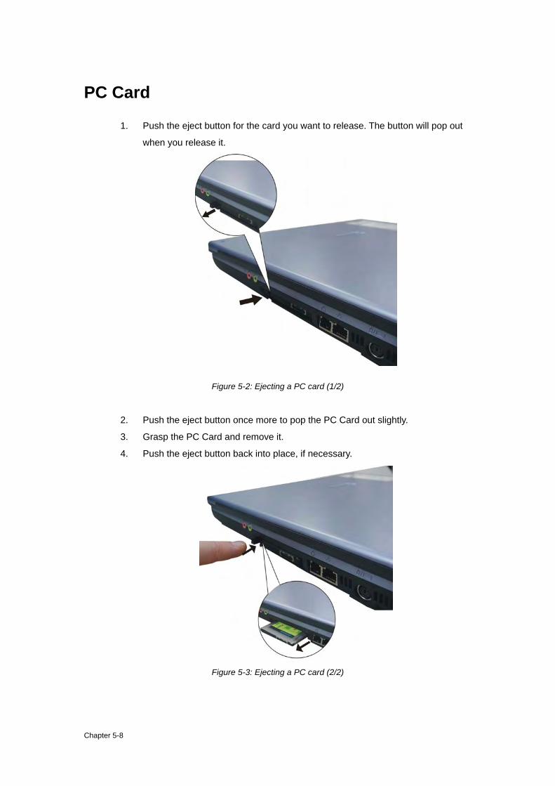
PC Card
1. Push the eject button for the card you want to release. The button will pop out
when you release it.
Figure 5-2: Ejecting a PC card (1/2)
2. Push the eject button once more to pop the PC Card out slightly.
3. Grasp the PC Card and remove it.
4. Push the eject button back into place, if necessary.
Figure 5-3: Ejecting a PC card (2/2)
Chapter 5-8

Display Assembly
The instructions and figures below are for the 15” display. Differences with the 14” display are indicated where necessary.
Removing the display assembly
1. Remove two M2.5×5 screws securing the strip cover.
Figure 5-4: Removing two screws securing the strip cover
Chapter 5-9
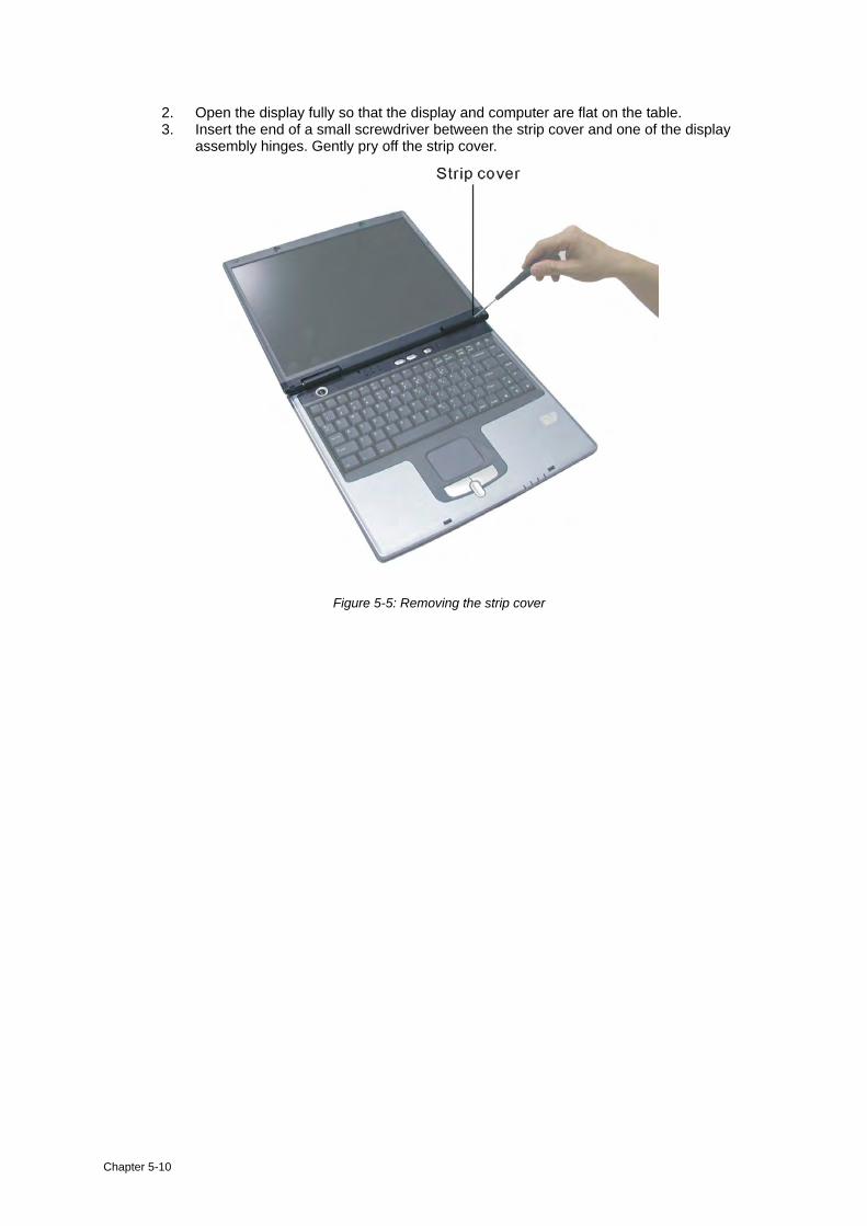
2. Open the display fully so that the display and computer are flat on the table. 3. Insert the end of a small screwdriver between the strip cover and one of the display
assembly hinges. Gently pry off the strip cover.
Figure 5-5: Removing the strip cover
Chapter 5-10

4. Lever the LCD display wire set connector off the system board connector. Do not pull on the wire itself as this may cause damage. Instead, pull on the connector white wire set connector.
5. Remove two M2.5×5 screws securing the display assembly hinges.
Figure 5-6: Releasing the LCD display wire set and hinges
Chapter 5-11

6. Turn the computer over. Remove two M2.5×9 screws from the base and two M2.5×7 screws from the rear panel.
Figure 5-7: Removing two screws securing the display assembly
7. Turn the computer upright. Open the display so that it is perpendicular to the desk, then gently lift off the display.
Figure 5-8: Lifting off the display assembly
Disassembling the display assembly
1. Remove two mask seals and two M2.5×7 screws securing the LCD bezel. If disassembling the 14” display, two M2.5×5 screws must also be removed from the top of the LCD bezel.
Chapter 5-12

Figure 5-9: Removing two screws securing the LCD bezel
2. Ease the bezel off the display, starting from one of the sides. The bezel is secured by latches, with four on each of the sides, seven along the bottom edge and six along the top edge.
Figure 5-10: Removing the LCD bezel
3. Remove the following eight screws securing the LCD module in the LCD cover: Two M2×3 screws from each side Two M2.5×5 screws from the upper corners Two M2.5×5 screws from the bottom corners
Chapter 5-13

Figure 5-11: Removing eight screws securing the LCD module
4. Lift the LCD module out of the LCD cover.
Chapter 5-14
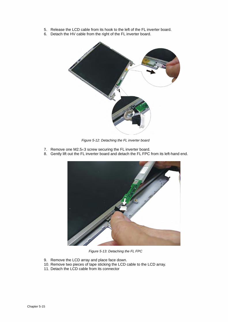
5. Release the LCD cable from its hook to the left of the FL inverter board. 6. Detach the HV cable from the right of the FL inverter board.
Figure 5-12: Detaching the FL inverter board
7. Remove one M2.5×3 screw securing the FL inverter board. 8. Gently lift out the FL inverter board and detach the FL FPC from its left-hand end.
Figure 5-13: Detaching the FL FPC
9. Remove the LCD array and place face down. 10. Remove two pieces of tape sticking the LCD cable to the LCD array. 11. Detach the LCD cable from its connector
Chapter 5-15
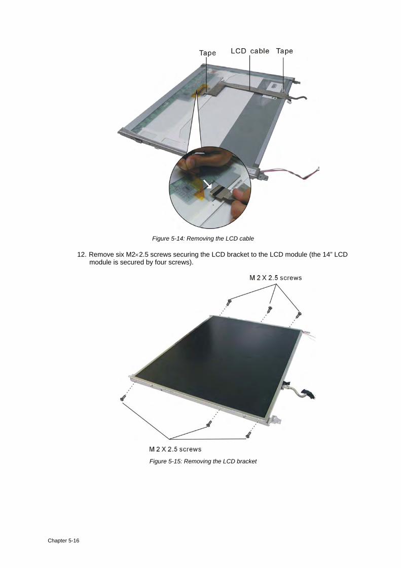
Figure 5-14: Removing the LCD cable
12. Remove six M2×2.5 screws securing the LCD bracket to the LCD module (the 14” LCD module is secured by four screws).
Figure 5-15: Removing the LCD bracket
Chapter 5-16

Keyboard / button board 1. Remove four M2.5×3 screws securing the keyboard.
Figure 5-16: Removing four screws securing the keyboard
Chapter 5-17

2. Lift the keyboard up and place higher on the computer base unit so that the keyboard cable connector is exposed.
3. Detach the keyboard cable and remove the keyboard.
Figure 5-17: Removing the keyboard
4. Remove two M2.5×3 screws securing the button board. Remove the button board.
Figure 5-18: Removing the button board
Chapter 5-18
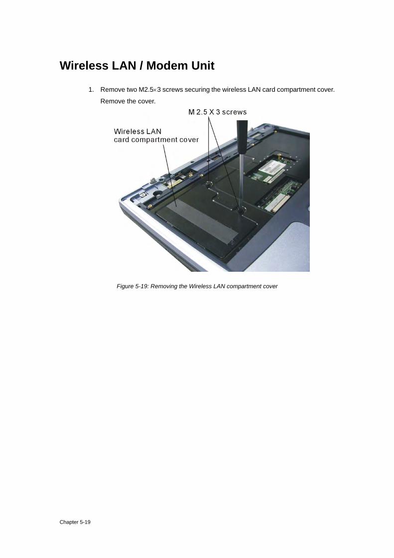
Wireless LAN / Modem Unit
1. Remove two M2.5×3 screws securing the wireless LAN card compartment cover.
Remove the cover.
Figure 5-19: Removing the Wireless LAN compartment cover
Chapter 5-19

2. Disconnect the modem cable.
3. If you will subsequently remove the top cover, you should peel back the tape
covering the Touch pad FFC and detach the FFC from its connector. If your aim is
solely to remove the Wireless LAN / modem card you do not need to detach the
FFC.
Figure 5-20: Disconnecting the Wireless LAN / modem card
Chapter 5-20
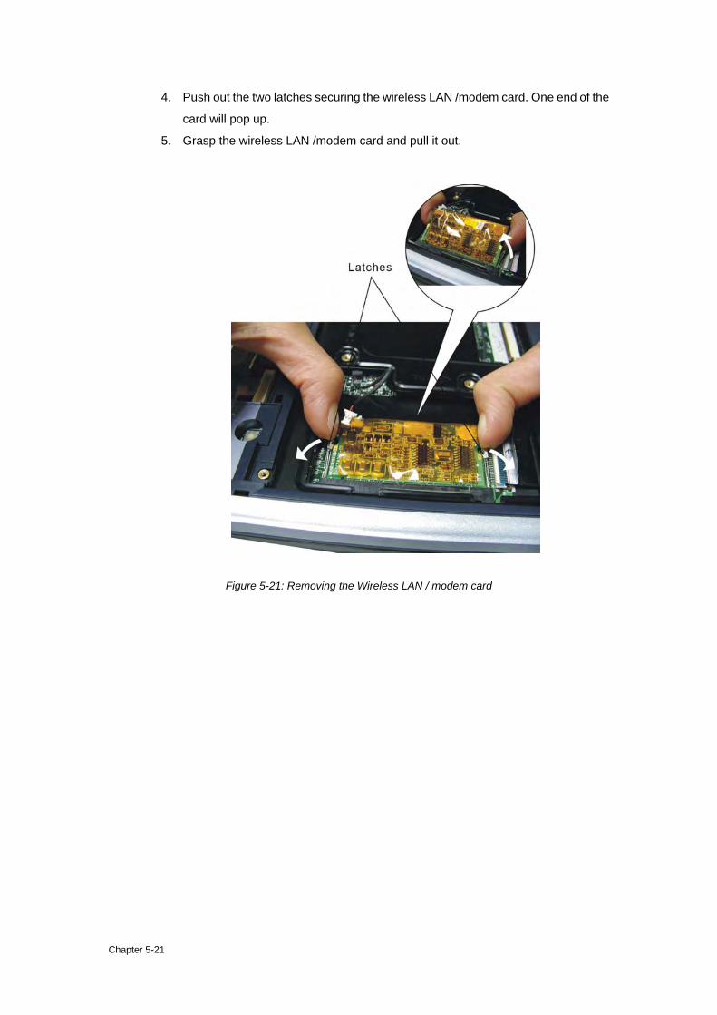
4. Push out the two latches securing the wireless LAN /modem card. One end of the
card will pop up.
5. Grasp the wireless LAN /modem card and pull it out.
Figure 5-21: Removing the Wireless LAN / modem card
Chapter 5-21

Expansion Memory
1. Remove one M2.5×5 screw securing the expansion memory compartment cover.
Lift off the cover.
Figure 5-22: Removing one screw securing the expansion memory compartment cover
Chapter 5-22
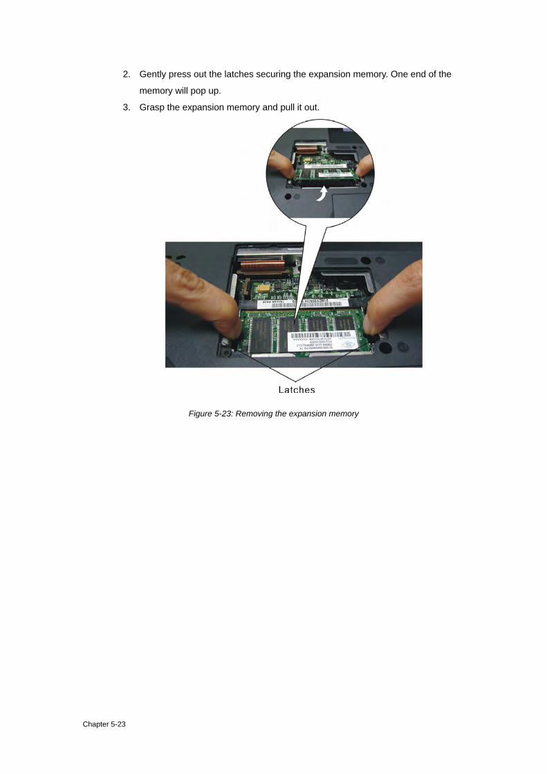
2. Gently press out the latches securing the expansion memory. One end of the
memory will pop up.
3. Grasp the expansion memory and pull it out.
Figure 5-23: Removing the expansion memory
Chapter 5-23

4. A spare expansion memory slot is located beneath the keyboard. To access this
remove the keyboard following the instructions in section 4.5. Remove the
memory card in the same way by easing the two latches apart.
Figure 5-24: Removing the spare expansion memory
Chapter 5-24
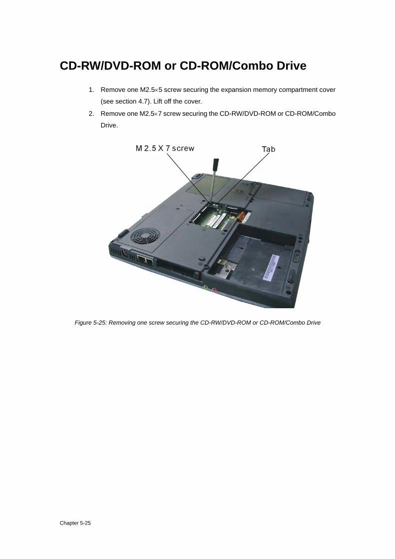
CD-RW/DVD-ROM or CD-ROM/Combo Drive
1. Remove one M2.5×5 screw securing the expansion memory compartment cover
(see section 4.7). Lift off the cover.
2. Remove one M2.5×7 screw securing the CD-RW/DVD-ROM or CD-ROM/Combo
Drive.
Figure 5-25: Removing one screw securing the CD-RW/DVD-ROM or CD-ROM/Combo Drive
Chapter 5-25

3. Push on the tab to push out the drive. Grasp the front of the drive to pull it fully
out.
Figure 5-26: Removing the CD-RW/DVD-ROM or CD-ROM/Combo Drive
4. Remove two M2.0×3 screws securing the drive bracket.
Figure 5-27: Removing the CD-RW/DVD-ROM or CD-ROM/Combo drive bracket
Chapter 5-26
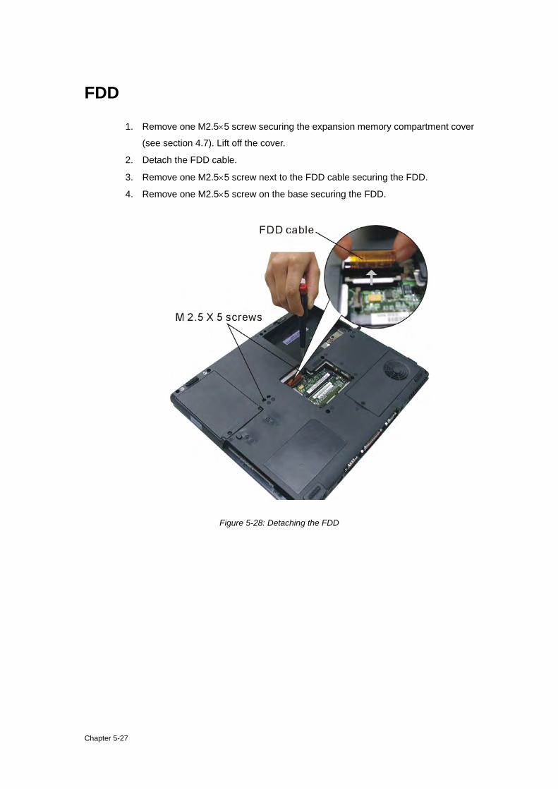
FDD
1. Remove one M2.5×5 screw securing the expansion memory compartment cover
(see section 4.7). Lift off the cover.
2. Detach the FDD cable.
3. Remove one M2.5×5 screw next to the FDD cable securing the FDD.
4. Remove one M2.5×5 screw on the base securing the FDD.
Figure 5-28: Detaching the FDD
Chapter 5-27
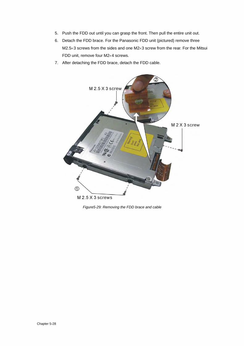
5. Push the FDD out until you can grasp the front. Then pull the entire unit out.
6. Detach the FDD brace. For the Panasonic FDD unit (pictured) remove three
M2.5×3 screws from the sides and one M2×3 screw from the rear. For the Mitsui
FDD unit, remove four M2×4 screws.
7. After detaching the FDD brace, detach the FDD cable.
Figure5-29: Removing the FDD brace and cable
Chapter 5-28
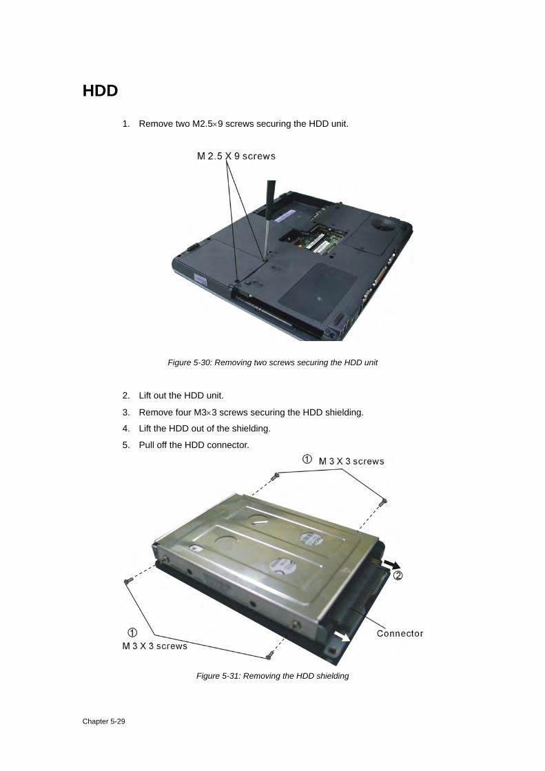
HDD
1. Remove two M2.5×9 screws securing the HDD unit.
Figure 5-30: Removing two screws securing the HDD unit
2. Lift out the HDD unit.
3. Remove four M3×3 screws securing the HDD shielding.
4. Lift the HDD out of the shielding.
5. Pull off the HDD connector.
Figure 5-31: Removing the HDD shielding
Chapter 5-29
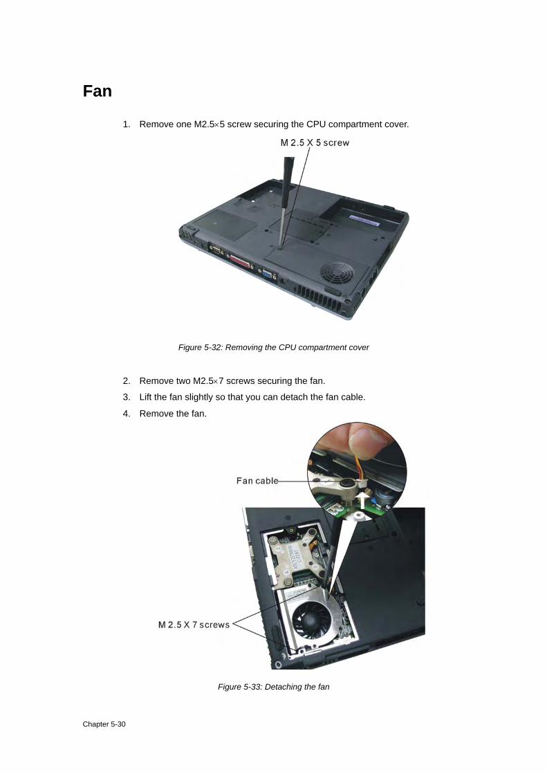
Fan
1. Remove one M2.5×5 screw securing the CPU compartment cover.
Figure 5-32: Removing the CPU compartment cover
2. Remove two M2.5×7 screws securing the fan.
3. Lift the fan slightly so that you can detach the fan cable.
4. Remove the fan.
Figure 5-33: Detaching the fan
Chapter 5-30

CPU
1. Remove one M2.5×5 screw securing the CPU compartment cover (see section
4.11).
2. Remove four screws securing the thermal unit
Figure 5-34: Removing four screws securing the thermal unit
3. Lift out the thermal unit.
Chapter 5-31
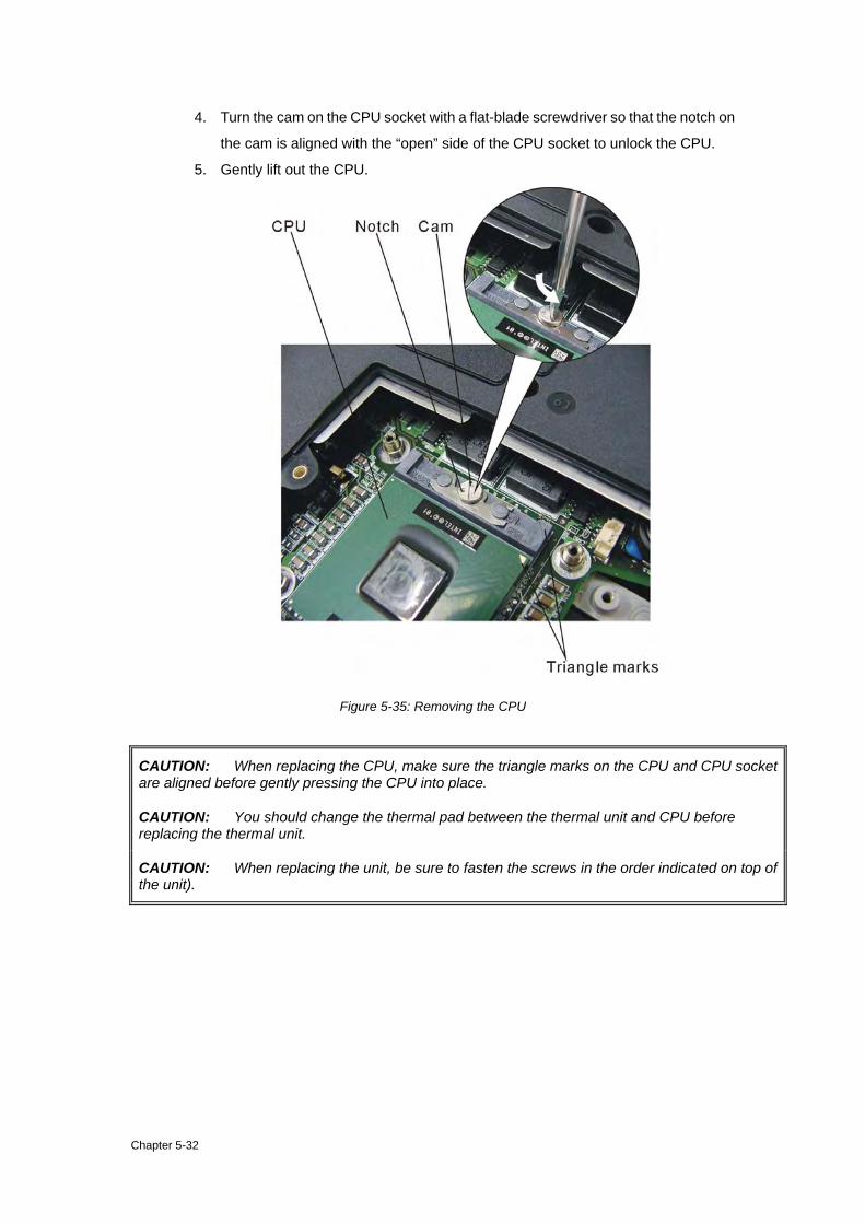
4. Turn the cam on the CPU socket with a flat-blade screwdriver so that the notch on
the cam is aligned with the “open” side of the CPU socket to unlock the CPU.
5. Gently lift out the CPU.
Figure 5-35: Removing the CPU
CAUTION: When replacing the CPU, make sure the triangle marks on the CPU and CPU socket are aligned before gently pressing the CPU into place.
CAUTION: You should change the thermal pad between the thermal unit and CPU before replacing the thermal unit.
CAUTION: When replacing the unit, be sure to fasten the screws in the order indicated on top of the unit).
Chapter 5-32
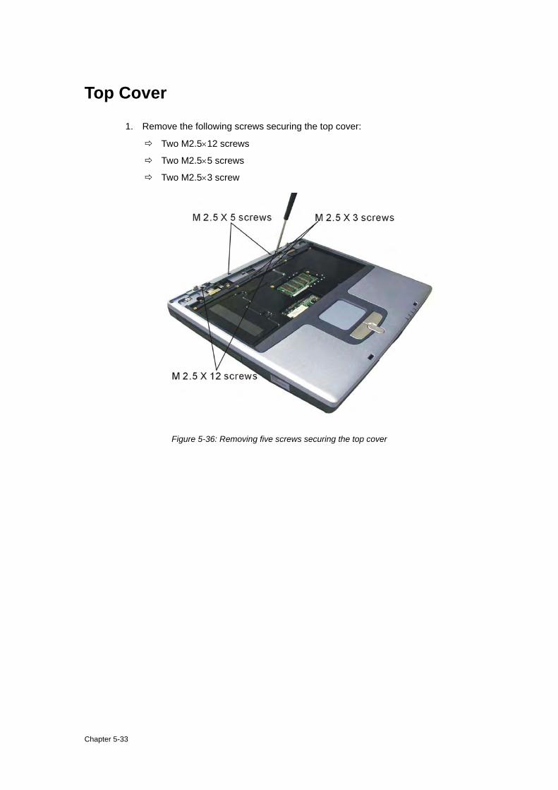
Top Cover
1. Remove the following screws securing the top cover:
Two M2.5×12 screws
Two M2.5×5 screws
Two M2.5×3 screw
Figure 5-36: Removing five screws securing the top cover
Chapter 5-33
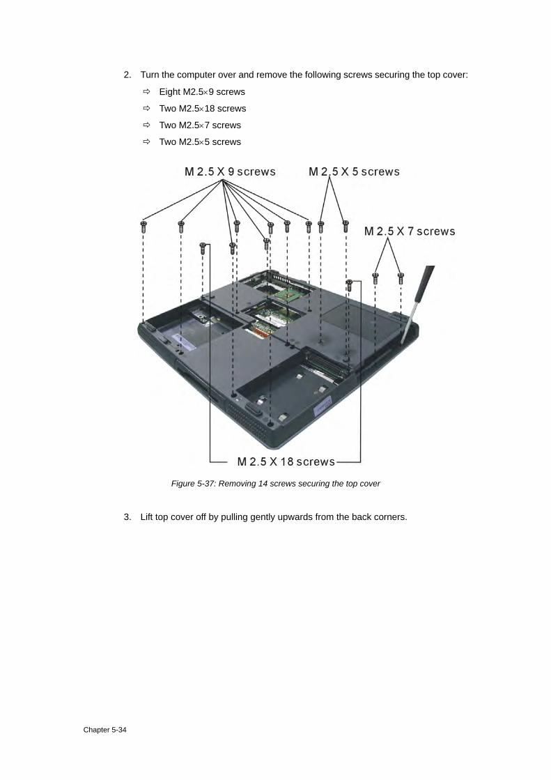
2. Turn the computer over and remove the following screws securing the top cover:
Eight M2.5×9 screws
Two M2.5×18 screws
Two M2.5×7 screws
Two M2.5×5 screws
Figure 5-37: Removing 14 screws securing the top cover
3. Lift top cover off by pulling gently upwards from the back corners.
Chapter 5-34
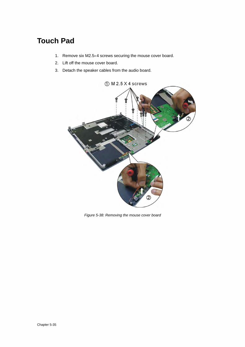
Touch Pad
1. Remove six M2.5×4 screws securing the mouse cover board.
2. Lift off the mouse cover board.
3. Detach the speaker cables from the audio board.
Figure 5-38: Removing the mouse cover board
Chapter 5-35
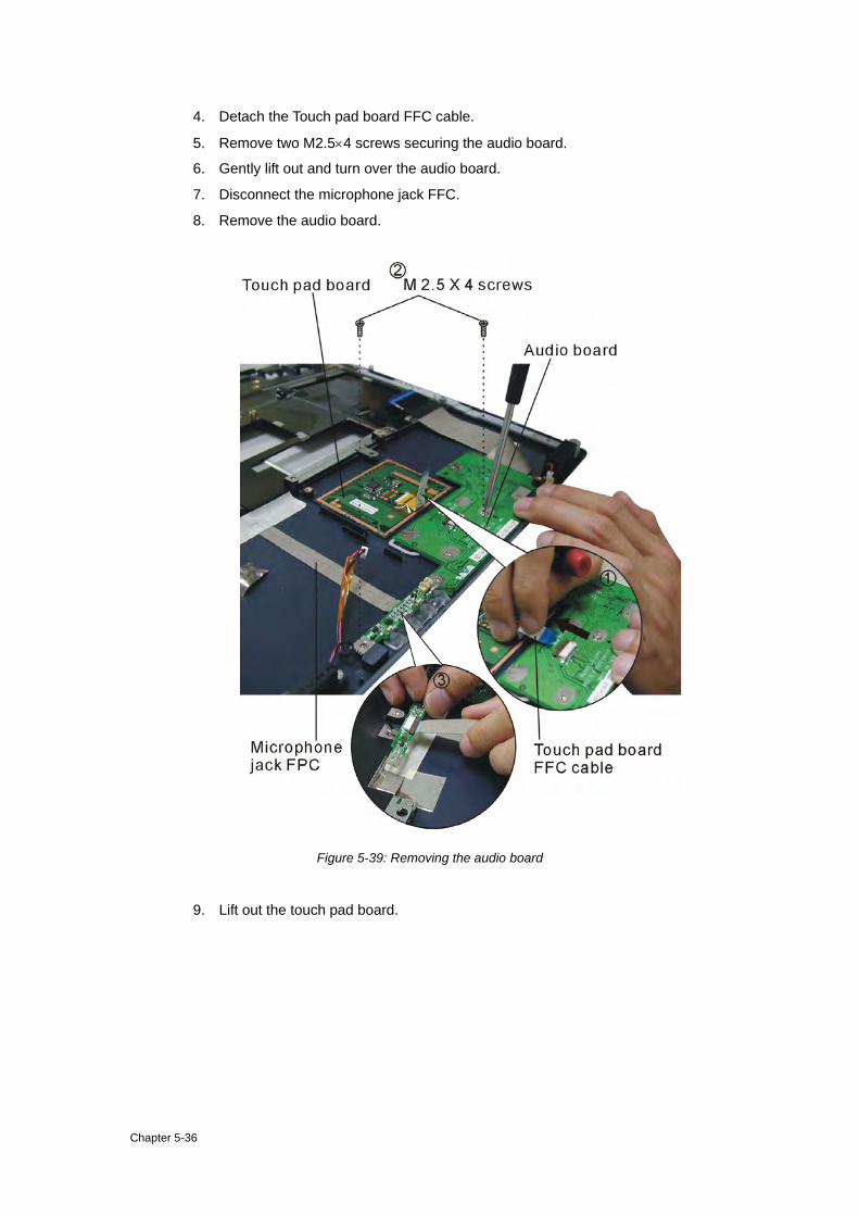
4. Detach the Touch pad board FFC cable.
5. Remove two M2.5×4 screws securing the audio board.
6. Gently lift out and turn over the audio board.
7. Disconnect the microphone jack FFC.
8. Remove the audio board.
Figure 5-39: Removing the audio board
9. Lift out the touch pad board.
Chapter 5-36
Speakers
1. Remove one M2.5×4 screw securing each of the speakers.
2. Detach both speaker cables from the audio board (you will already have
detached the cables if you have removed the audio board).
Figure 5-40: Removing the speakers
3. Lift out the speakers.
Chapter 5-37
Microphone jack
1. Remove two M2.5×4 screws securing the microphone jack.
2. Peel off the tape securing the microphone jack FFC.
3. Remove the microphone jack.
Figure 5-41: Removing the microphone jack
Chapter 5-38
System Board
1. Remove three M2.5×5 screws securing the system board
2. Remove six helix screw nuts securing the rear ports.
3. Remove the system board by lifting from the center of the inside edge of the
board.
Figure 5-42: Removing the system board
Chapter 5-39
Chapter 6: Testing and Troubleshooting The purpose of this chapter is to provide a systematic method of isolating problems you may have with the ACY25 series Notebook Computer. We assume that you have a basic understanding of DOS-based computer systems as well as knowledge of standard trouble-shooting procedures. This manual is written under the assumption that the problems are indeed related with Notebook itself. The improper usage and application software problems are excluded in this chapter. The system BIOS Beep Code is an integrated unit to detect some errors in the system board. This beep code will give immediate identification of certain system board problems. If the troubleshooting procedure is followed step by step, it can efficiently isolate the problem and the problem can be solved easily.
PERFORM VISUAL INSPECTION Check the following: Power cords are properly connected and secured Power supply is adequate for operation There are no obvious shorts or opens There are no obviously burned or heated components All components appear normal
Troubleshooting Flowchart Use the flowchart in Figure 6-1 as a guide for determining which troubleshooting procedures to execute. Before going through the flowchart steps, verify the following:
• Ask the user if a password is registered and, if it is, ask him or her to enter the password.
• Verify with the customer that Windows XP is installed on the hard disk. Operating systems that were not preinstalled by Compal can cause the computer to malfunction.
• Make sure all optional equipment is removed from the computer.
• Make sure the floppy disk drive is empty.
Chapter 6-1
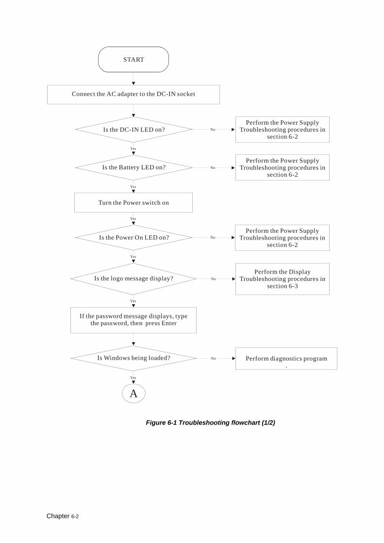
START
Connect the AC adapter to the DC-IN socket
Is the DC-IN LED on?
Is Windows being loaded?
Is the Power On LED on?
Is the logo message display?
If the password message displays, typethe password, then press Enter
A
Is the Battery LED on?
Turn the Power switch on
Perform the Power SupplyTroubleshooting procedures in
section 6-2
Perform the DisplayTroubleshooting procedures in
section 6-3
Perform diagnostics program.
Yes
Yes
Yes
Yes
Yes
Yes
No
No
No
No
No
Perform the Power SupplyTroubleshooting procedures in
section 6-2
Perform the Power SupplyTroubleshooting procedures in
section 6-2
Figure 6-1 Troubleshooting flowchart (1/2)
Chapter 6-2
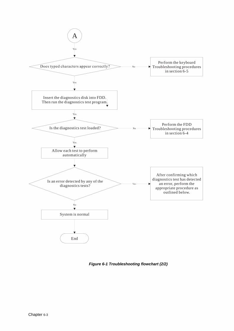
End
Insert the diagnostics disk into FDD.Then run the diagnostics test program.
Is an error detected by any of thediagnostics tests?
System is normal
A
Is the diagnostics test loaded?
Allow each test to performautomatically
Yes
No
No
Perform the keyboardTroubleshooting procedures
in section 6-5
Perform the FDDTroubleshooting procedures
in section 6-4
After confirming whichdiagnostics test has detected
an error, perform the appropriate procedure as
outlined below.
Yes
Yes
Yes
No
Figure 6-1 Troubleshooting flowchart (2/2)
Chapter 6-3

If the diagnostics program cannot detect an error, the problem may be intermittent. The test program should be executed several times to isolate the problem. When a problem has been located, perform the appropriate troubleshooting procedures as follows: 1. If an error is detected by the main battery test, perform the Power Supply
Troubleshooting procedures in Section 6-2.
2. If an error is detected by the display test, perform the Display Troubleshooting procedures in Section 6-3.
3. If an error is detected by the floppy disk test, perform the FDD Troubleshooting procedures in Section 6-4.
4. If an error is detected by the keyboard test, perform the Keyboard Troubleshooting procedures in Section 6-5.
5. If an error is detected by the printer (parallel) port test, perform the Printer Port Troubleshooting procedures in Section 6-8.
6. If an error is detected by the CD-ROM/DVD-ROM test, perform the DVD-ROM and CD-RW/DVD-ROM Troubleshooting Procedures in Section 6-11.
7. If an error is detected by the Modem test, perform the Modem Troubleshooting Procedures in Section 6-12 or the LAN Troubleshooting Procedures in Section 2.11.
8. If an error is detected by the Sound test, perform the Sound Troubleshooting Procedures in Section 2.12.
Other problems that are not covered by the diagnostics program may be discovered by a user.
1. If an error is detected when using an external USB device, perform the External USB Devices Troubleshooting procedures in Section 6-6.
2. If an error is detected when using the TV-out connection, perform the TV-Out Failure Troubleshooting procedures in Section 6-7.
3. If an error is detected when using the touch pad, perform the Touch Pad Troubleshooting procedures in Section 6-9.
4. If an error is detected when using the speakers, perform the Speaker Troubleshooting procedures in Section 6-10.
5. If an error is detected when using the CD/DVD drive, perform the CD-ROM/DVD Drive Troubleshooting procedures in Section 6-11.
6. If an error is detected when using the modem, perform the Modem Troubleshooting procedures in Section 6-12.
7. If an error is detected when using the PCMCIA unit, perform the PCMCIA Troubleshooting procedures in Section 6-13.
Chapter 6-4
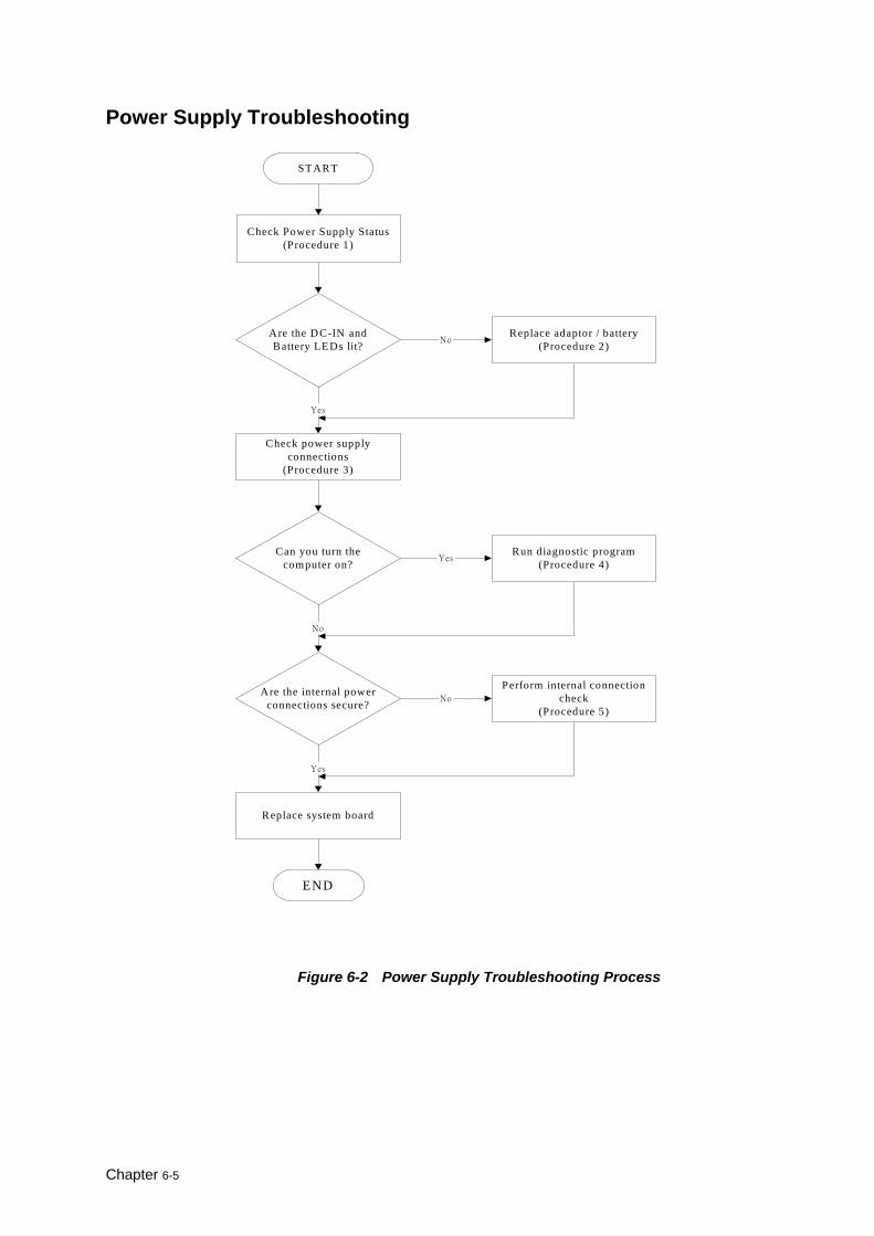
Power Supply Troubleshooting
START
Are the DC-IN andBattery LEDs lit?
Can you turn thecomputer on?
Are the internal powerconnections secure?
END
Check Power Supply Status(Procedure 1)
No
Yes
Check power supplyconnections
(Procedure 3)
Run diagnostic program(Procedure 4)
Yes
No
Replace adaptor / battery(Procedure 2)
No
Perform internal connectioncheck
(Procedure 5)
Replace system board
Yes
Figure 6-2 Power Supply Troubleshooting Process
Chapter 6-5
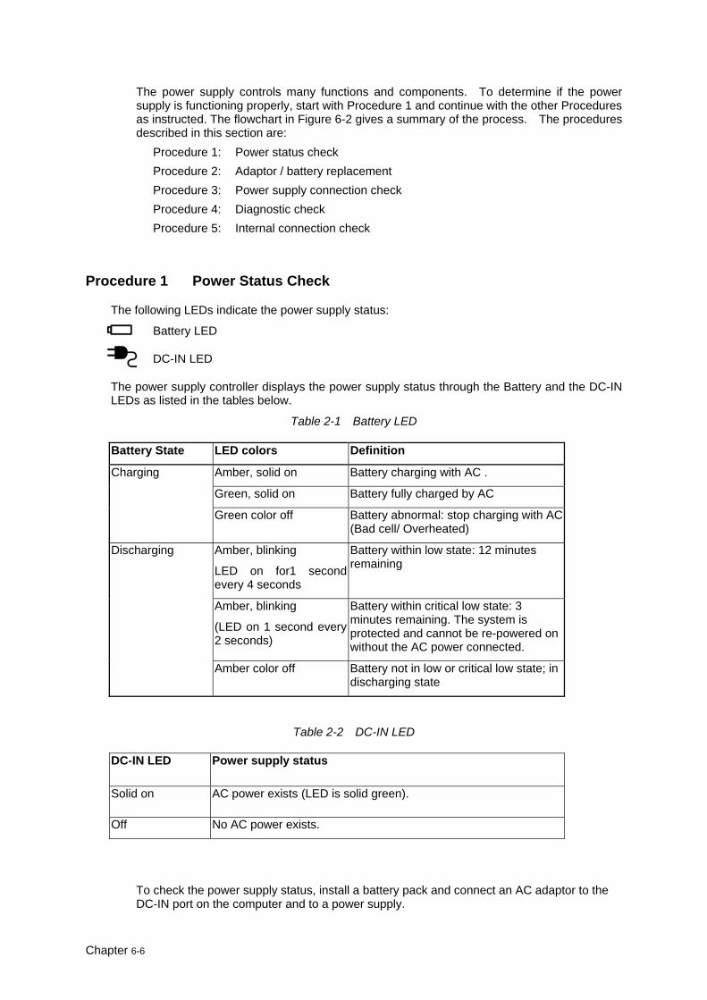
The power supply controls many functions and components. To determine if the power supply is functioning properly, start with Procedure 1 and continue with the other Procedures as instructed. The flowchart in Figure 6-2 gives a summary of the process. The procedures described in this section are:
Procedure 1: Power status check Procedure 2: Adaptor / battery replacement Procedure 3: Power supply connection check Procedure 4: Diagnostic check Procedure 5: Internal connection check
Procedure 1 Power Status Check
The following LEDs indicate the power supply status:
Battery LED
DC-IN LED
The power supply controller displays the power supply status through the Battery and the DC-IN LEDs as listed in the tables below.
Table 2-1 Battery LED
Battery State LED colors Definition
Amber, solid on Battery charging with AC .
Green, solid on Battery fully charged by AC
Charging
Green color off Battery abnormal: stop charging with AC (Bad cell/ Overheated)
Amber, blinking
LED on for1 second every 4 seconds
Battery within low state: 12 minutes remaining
Amber, blinking
(LED on 1 second every 2 seconds)
Battery within critical low state: 3 minutes remaining. The system is protected and cannot be re-powered on without the AC power connected.
Discharging
Amber color off Battery not in low or critical low state; in discharging state
Table 2-2 DC-IN LED
DC-IN LED Power supply status
Solid on AC power exists (LED is solid green).
Off No AC power exists.
To check the power supply status, install a battery pack and connect an AC adaptor to the DC-IN port on the computer and to a power supply.
Chapter 6-6
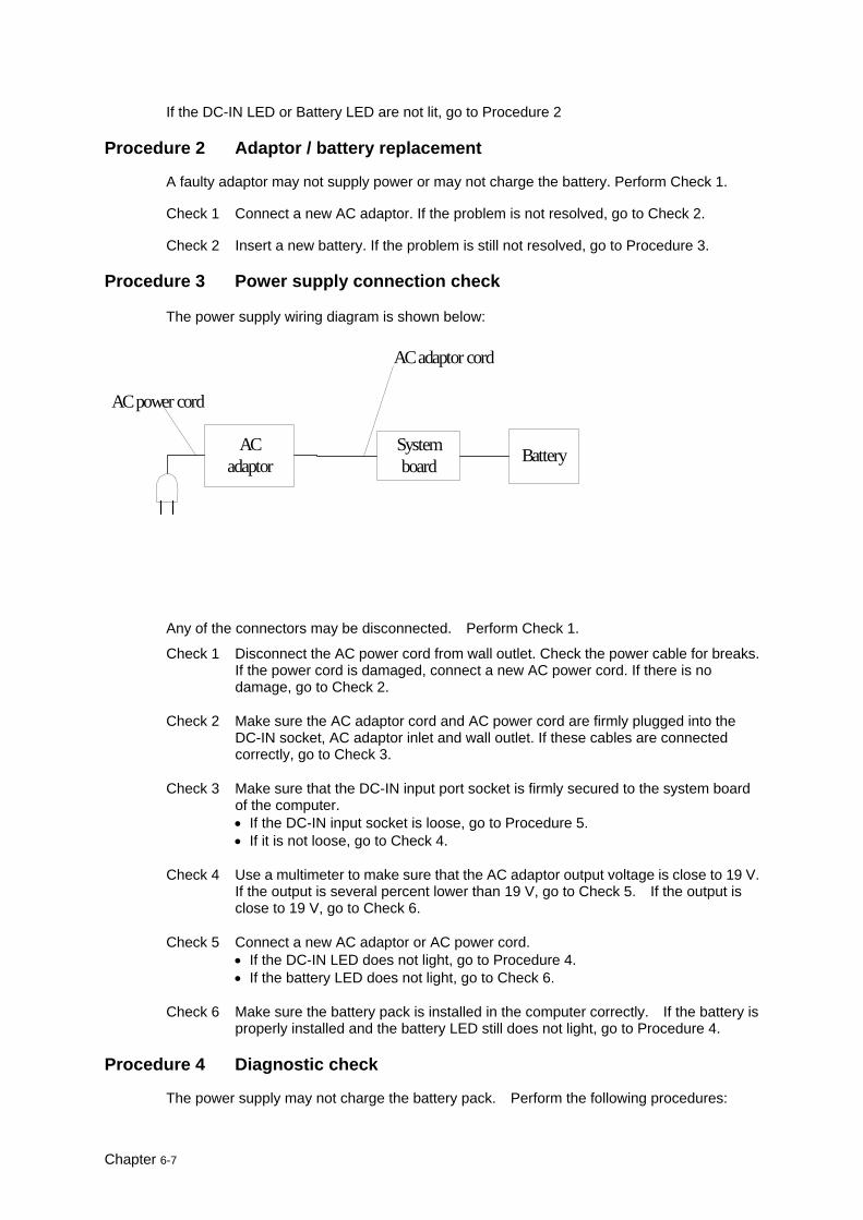
If the DC-IN LED or Battery LED are not lit, go to Procedure 2
Procedure 2 Adaptor / battery replacement
A faulty adaptor may not supply power or may not charge the battery. Perform Check 1.
Check 1 Connect a new AC adaptor. If the problem is not resolved, go to Check 2.
Check 2 Insert a new battery. If the problem is still not resolved, go to Procedure 3.
Procedure 3 Power supply connection check
The power supply wiring diagram is shown below:
ACadaptor
Systemboard Battery
AC adaptor cord
AC power cord
Any of the connectors may be disconnected. Perform Check 1.
Check 1 Disconnect the AC power cord from wall outlet. Check the power cable for breaks. If the power cord is damaged, connect a new AC power cord. If there is no damage, go to Check 2.
Check 2 Make sure the AC adaptor cord and AC power cord are firmly plugged into the DC-IN socket, AC adaptor inlet and wall outlet. If these cables are connected correctly, go to Check 3.
Check 3 Make sure that the DC-IN input port socket is firmly secured to the system board of the computer. • If the DC-IN input socket is loose, go to Procedure 5. • If it is not loose, go to Check 4.
Check 4 Use a multimeter to make sure that the AC adaptor output voltage is close to 19 V. If the output is several percent lower than 19 V, go to Check 5. If the output is close to 19 V, go to Check 6.
Check 5 Connect a new AC adaptor or AC power cord. • If the DC-IN LED does not light, go to Procedure 4. • If the battery LED does not light, go to Check 6.
Check 6 Make sure the battery pack is installed in the computer correctly. If the battery is properly installed and the battery LED still does not light, go to Procedure 4.
Procedure 4 Diagnostic check
The power supply may not charge the battery pack. Perform the following procedures:
Chapter 6-7

1. Reinstall the battery pack.
2. Attach the AC adaptor and turn on the power. If you cannot turn on the power, go to Procedure 5.
3. Run the Diagnostic test following the procedures described Tests and Diagnostics. If no problem is detected, the battery is functioning normally.
Procedure 5 Replacement check
The system board may be disconnected or damaged. Disassemble the computer following the steps described Replacement Procedures. Check the connection between the AC adaptor and the system board. After checking the connection, perform Check 1: Check 1 Use a multimeter to make sure that the fuses on the system board are not blown.
If a fuse is not blown, go to Check 2. If a fuse is blown, go to Check 3.
Check 2 Make sure that the battery cable is firmly connected to the system board. If it is connected firmly, go to Check 3.
Check 3 The system board may be damaged. Replace it with a new one following the instructions in Chapter 4.
Chapter 6-8
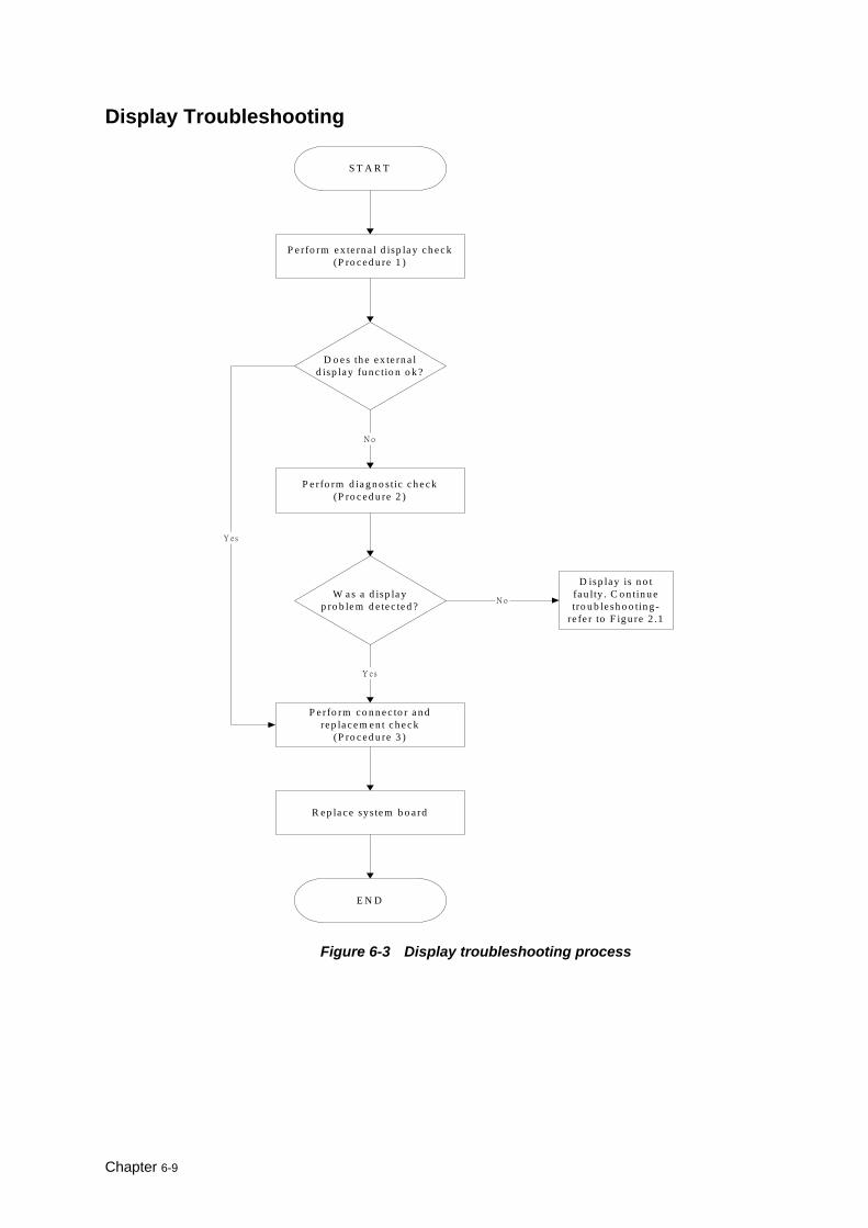
Display Troubleshooting
P e rfo rm e x te rn a l d isp la y c h e c k(P ro c e d u re 1 )
S T A R T
D o e s th e e x te rn a ld isp la y fu n c tio n o k ?
P e rfo rm d ia g n o s tic c h e c k(P ro c e d u re 2 )
N o
W a s a d isp la yp ro b le m d e te c te d ?
P e rfo rm c o n n e c to r a n dre p la c e m e n t c h e c k
(P ro c e d u re 3 )
R e p la c e sys te m b o a rd
E N D
Y es
Y es
N o
D isp la y is n o tfa u lty . C o n tin u etro u b le sh o o tin g -
re fe r to F ig u re 2 .1
Figure 6-3 Display troubleshooting process
Chapter 6-9
This section describes how to determine if the computer’s display is functioning properly. The process is outlined in Figure 6-3. Start with Procedure 1 and continue with the other procedures as instructed.
Procedure 1: External display check Procedure 2: Diagnostic check Procedure 3: Connector and replacement check
Procedure 1 External display check
Connect an external display to the computer’s external monitor port, then boot the computer. The computer automatically detects the external display. Press Fn+F5 to switch to the external display.
If the external display works correctly, the internal LCD may be damaged. Go to Procedure 3.
If the external monitor appears to have the same problem as the internal monitor, the system board may be damaged. Go to Procedure 2.
Procedure 2 Diagnostic check
The Display Test program is stored on the computer’s Diagnostics disk. This program checks the display controller on the system board. Insert the Diagnostics disk in the computer’s floppy disk drive, turn on the computer and run the test. Refer to Chapter 3, Tests and Diagnostics for details.
If an error is detected, go to Procedure 3. If an error is not detected, the display is functioning properly.
Procedure 3 Connector and replacement check
The FL inverter board, LCD module, and system board are connected to the display circuits. Any of these components may be damaged. Replacement Procedures, for instructions on how to disassemble the computer and then perform the following checks:
Check 1 Make sure the DDRRAM module is seated properly. Test display again. If the problem still exits, replace the DDRRAM module. If the problem still exists, perform check 2.
Check 2 Replace the FL inverter board with a new one and test display again. If the problem still exists, perform Check 3.
Check 3 Replace the LCD module with a new one and test display again. If the problem still exists, perform Check 4.
Check 4 Replace the LCD/FL cable with a new one and test display again. If the problem still exists, perform Check 5.
Check 5 Replace the CPU with another of the same specifications. If the problem still exists, perform Check 6.
Check 6 The system board may be damaged. Replace it with a new one.
Chapter 6-10
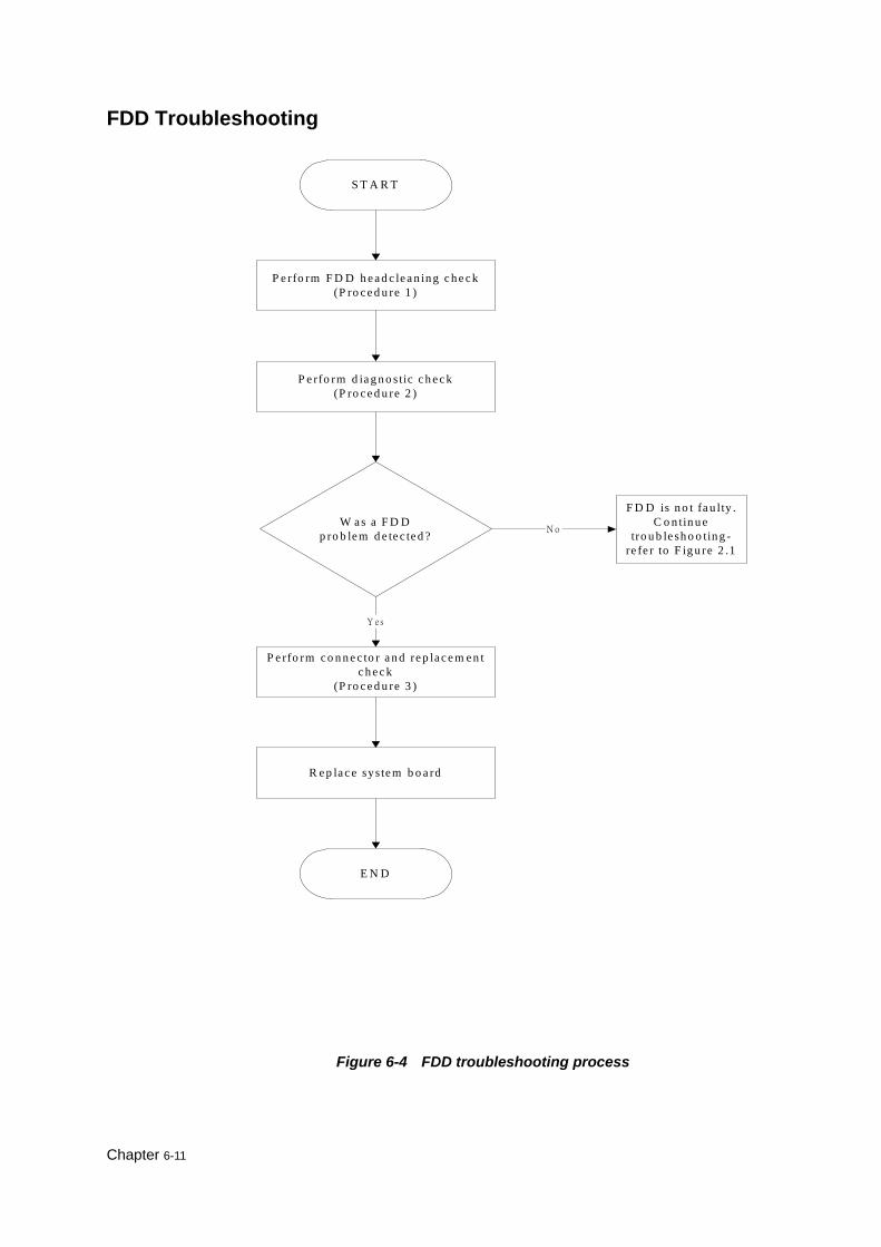
FDD Troubleshooting
P e rfo rm F D D h e a d c le a n in g c h e c k(P ro c e d u re 1 )
S T A R T
W a s a F D Dp ro b le m d e te c te d ?
P e rfo rm c o n n e c to r a n d re p la c e m e n tc h e c k
(P ro c e d u re 3 )
R e p la c e sys te m b o a rd
E N D
Y es
N o
F D D is n o t fa u lty .C o n tin u e
tro u b le sh o o tin g -re fe r to F ig u re 2 .1
P e rfo rm d ia g n o s tic c h e c k(P ro c e d u re 2 )
Figure 6-4 FDD troubleshooting process
Chapter 6-11
This section describes how to determine if the FDD is functioning properly. Perform the steps below starting with Procedure 1 and continuing as required. Figure 6-4 gives an outline of the process.
Procedure 1: FDD head cleaning check Procedure 2: Diagnostic check Procedure 3: Connector check and replacement check
Procedure 1 FDD head cleaning check
The FDD heads can become dirty over time, affecting their performance. Use an FDD cleaning kit to clean the heads. If the FDD still does not function properly after cleaning, go to Procedure 2.
Procedure 2 Diagnostic check
Insert the Diagnostics Disk in the FDD, turn on the computer and run the test.
If no FDD problem is detected by the diagnostic test, the FDD is functioning normally. If an error occurs, go to Procedure 3.
Procedure 3 Connector check and replacement check
The 3.5-inch FDD is connected to the system board. For instructions on how to disassemble the computer and then perform the following checks:
Check 1 Make sure the FDD flexible cable is firmly connected to the FDD and system board. If any of the connections are loose, reconnect firmly and repeat Procedure 2. If any of the connections is damaged, or there is still an error, go to Check 2.
Check 2 The FDD unit or FDD flexible cable may be defective or damaged. If the FDD is still not functioning properly, perform Check 3.
Check 3 Replace the system board.
Chapter 6-12
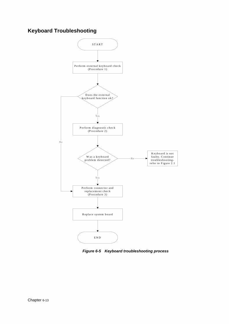
Keyboard Troubleshooting
P e rfo rm e x te rn a l k e y b o a rd c h e c k(P ro c e d u re 1 )
S T A R T
D o e s th e e x te rn a lk e yb o a rd fu n c tio n o k ?
P e rfo rm d ia g n o s tic c h e c k(P ro c e d u re 2 )
W a s a k e y b o a rdp ro b le m d e te c te d ?
P e rfo rm c o n n e c to r a n dre p la c e m e n t c h e c k
(P ro c e d u re 3 )
R e p la c e sys te m b o a rd
E N D
Y es
N o
K e yb o a rd is n o tfa u lty . C o n tin u etro u b le sh o o tin g -
re fe r to F ig u re 2 .1
N o
Y es
Figure 6-5 Keyboard troubleshooting process
Chapter 6-13
To determine if the computer’s keyboard is functioning properly, perform the following procedures. Figure 6-5 outlines the process. Start with Procedure 1 and continue with the other procedures as instructed.
Procedure 1: External keyboard check
Procedure 2: Diagnostic check
Procedure 3: Connector and replacement check
Procedure 1 External keyboard check
Connect a USB keyboard to one of the computer’s keyboard/mouse ports, then boot the computer. The computer automatically detects the external keyboard.
If the external keyboard works correctly, the internal keyboard or its connections may be faulty. Go to Procedure 2.
If the external keyboard appears to have the same problem as the internal keyboard, the system board may be damaged.
Procedure 2 Diagnostic test
Run the Diagnostic Program, which will automatically execute the Keyboard Test. Refer to Chapter 3, Tests and Diagnostics for more information on how to run the program.
If an error is located, go to Procedure 3. If an error does not occur, the keyboard is functioning properly.
Procedure 3 Connector and replacement check
The keyboard and/or system board may be disconnected or damaged. Replacement Procedures and perform the following checks.
Check 1 Make sure the keyboard cable is firmly connected to the system board.
If the connection is loose, reconnect firmly and repeat Procedure 2. If there is still an error, go to Check 2.
Check 2 The keyboard may be damaged.
If the problem still exists, perform Check 3.
Check 3 The system board may be damaged. R
Chapter 6-14
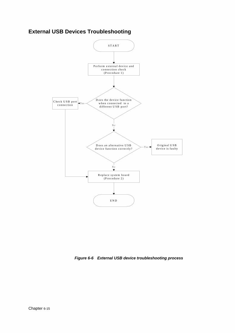
External USB Devices Troubleshooting
R e p la c e sys te m b o a rd(P ro c e d u re 2 )
E N D
O rig in a l U S Bd e v ic e is fa u lty
P e rfo rm e x te rn a l d e v ic e a n dc o n n e c tio n c h e c k
(P ro c e d u re 1 )
S T A R T
D o e s th e d e v ic e fu n c tio nw h e n c o n n e c te d to ad iffe re n t U S B p o rt?
D o e s a n a lte rn a tiv e U S Bd e v ic e fu n c tio n c o r re c tly?
N o
Y es
N o
C h e c k U S B p o rtc o n n e c tio n
Y es
Figure 6-6 External USB device troubleshooting process
Chapter 6-15
To determine if the computer’s external USB devices are functioning properly, perform the following procedures. Figure 6-6 outlines the process. Start with Procedure 1 and continue as instructed.
Procedure 1: External device and connection check
Procedure 2: Replace system board
Procedure 1 External device and connection check
The USB device may be damaged or the connection may be faulty. Perform Check 1.
Check 1 Make sure USB device cable is firmly plugged into one of the USB sockets. If the cable is connected correctly, go to Check 2.
Check 2 Plug the USB device into another USB socket (there are three in all). If the USB device still does not work, go to Check 4.
If the device functions correctly when connected to another USB port, go to Check 3
Check 3 Make sure that the USB socket is firmly secured to the system board of the computer. If the malfunction remains, the system board may be damaged. Go to Procedure 2.
Check 4 Connect an alternative USB device to one of the computer’s USB ports, and then boot the computer. The computer automatically detects the external device.
If the alternative USB device works correctly, the original device may be damaged and should be replaced.
If the alternative USB device appears to have the same problem as the original device, the system board may be damaged. Go to Procedure 2.
Procedure 2 Replace system board
If the error persists, the system board may be damaged.
Chapter 6-16

TV-Out Failure Troubleshooting
P e rfo rm T V c o n n e c tio n c h e c k(P ro c e d u re 1 )
S T A R T
D o e s re p la c e m e n t T V c a b lefu n c tio n p ro p e rly?
P e rfo rm T V se t c h e c k(P ro c e d u re 2 )
R e p la c e sys te m b o a rd
E N D
N o R e p la c e T V c a b le
N o
T V fu n c tio n in g o k ?
Y es
U se d iffe re n t T Vse t
N o
Figure 6-7 TV-out troubleshooting process
Chapter 6-17

To determine if the computer’s TV-out port is functioning properly, perform the following procedures. Figure 6-7 outlines the process. Start with Procedure 1 and continue as instructed.
Procedure 1: TV connection check
Procedure 2: TV set check
Procedure 1 TV connection check
The TV cable may be damaged or the connections may be loose. Perform Check 1:
Check 1 Make sure TV cable is firmly plugged into both the TV set and the TV-out port of the computer. If the cable is connected correctly, go to Check 2.
Check 2 Make sure the TV-out port is firmly secured to the system board of the computer. If the malfunction remains, go to Check 3.
Check 3 The TV cable may be damaged. Replace with a good cable. If the malfunction remains, go to Procedure 2
Procedure 2 TV set check
The TV set may be faulty. Perform Check 1:
Check 1 Try using the set for television reception. If it does not work, the set may be damaged. If the set does work, perform Check 2.
Check 2 Try connecting a different television to the computer. If the replacement television works, the original set may be damaged. If the replacement set does not work the system board may be damaged.
Chapter 6-18
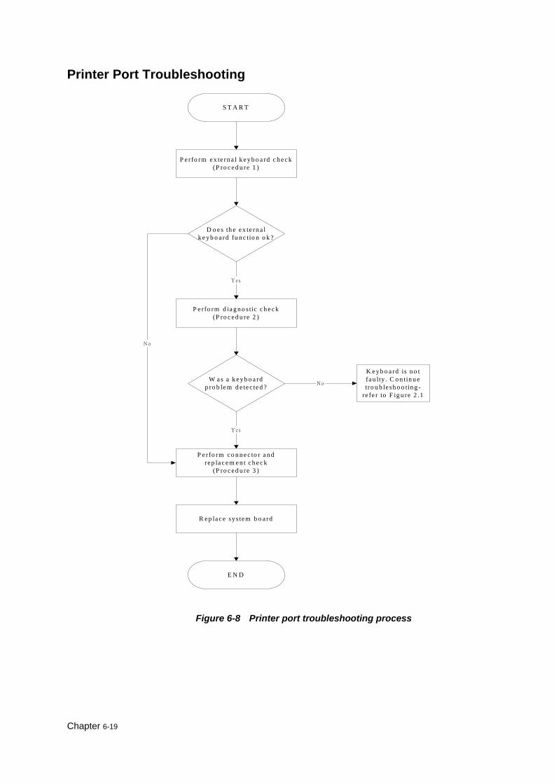
Printer Port Troubleshooting
P e rfo rm e x te rn a l k e y b o a rd c h e c k(P ro c e d u re 1 )
S T A R T
D o e s th e e x te rn a lk e yb o a rd fu n c tio n o k ?
P e rfo rm d ia g n o s tic c h e c k(P ro c e d u re 2 )
W a s a k e y b o a rdp ro b le m d e te c te d ?
P e rfo rm c o n n e c to r a n dre p la c e m e n t c h e c k
(P ro c e d u re 3 )
R e p la c e sys te m b o a rd
E N D
Y es
N o
K e yb o a rd is n o tfa u lty . C o n tin u etro u b le sh o o tin g -
re fe r to F ig u re 2 .1
N o
Y es
Figure 6-8 Printer port troubleshooting process
Chapter 6-19
To determine if the computer’s printer (parallel) port is functioning properly, perform the following procedures. Figure 6-8 outlines the process. Start with Procedure 1 and continue as instructed.
Procedure 1: Diagnostic test
Procedure 2: Printer and connection test
Procedure 3: Replace system board
Procedure 1 Diagnostic test
Attach the printer port loopback connector firmly to the printer port and run the Diagnostic Program. If the printer port test passes, there may be a problem with the printer. Go to Procedure 2. If the printer port test fails, go to Procedure 3.
Procedure 2 Printer and connection test
The printer may be faulty or not connected properly. Perform Check 1.
Check 1 Make sure printer cable is firmly plugged into both the printer and the printer port of the computer. If the cable is connected correctly, go to Check 2.
Check 2 Make sure the printer port is firmly secured to the system board of the computer. If the malfunction remains, go to Check 3.
Check 3 The printer cable may be damaged. Replace with a good cable. If the malfunction remains, go to Check 4.
Check 4 The printer may be faulty. Replace it with a good printer or connect it to a different computer.
If the replacement printer works or the original printer does not work on a different computer, the printer should be replaced.
If the replacement printer does not work either, or the original printer functions normally on a different computer, go to Procedure 3.
Procedure 3 Replace system board
The system board may be damaged.
Chapter 6-20

Touch Pad Troubleshooting
START
END
Touch Pad connectioncheck (Procedure 1)
Touch Pad replacementcheck (Procedure 2)
Replace system board
Figure 6-9 Touch Pad troubleshooting process
Chapter 6-21
To determine if the computer’s built-in Touch Pad is functioning properly, perform the following procedures. Figure 6-9 outlines the process. Start with Procedure 1 and continue as instructed.
Procedure 1: Touch Pad connection check
Procedure 2: Touch Pad replacement check
Procedure 1 Touch Pad connection check
The Touch Pad is connected by the Touch Pad FPC to the system board. Make sure the Touch Pad FPC cable is firmly connected to the Touch Pad and system board. Replacement Procedures, for instructions on how to disassemble the computer and then perform the following checks.
If any of the connections are loose, reconnect firmly. If any of the connections is damaged, or there is still an error, go to Procedure 2.
Procedure 2 Touch Pad replacement check
The Touch Pad unit or FPC may be defective or damaged.
Chapter 6-22
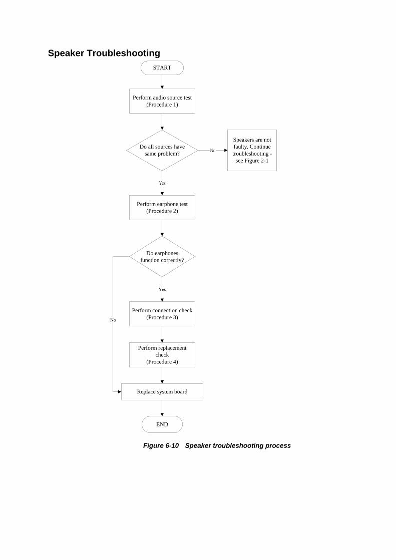
Speaker Troubleshooting START
Do all sources havesame problem?
END
Perform earphone test(Procedure 2)
Do earphonesfunction correctly?
Perform connection check(Procedure 3)
Perform replacementcheck
(Procedure 4)
Perform audio source test(Procedure 1)
No
Yes
Yes
Replace system board
Speakers are notfaulty. Continuetroubleshooting -
see Figure 2-1
No
Figure 6-10 Speaker troubleshooting process
To determine if the computer’s built-in speakers are functioning properly, perform the following procedures. Figure 6-10 outlines the process. First adjust the speaker volume to an appropriate level. Start with Procedure 1 and continue as instructed.
Procedure 1: Audio source test
Procedure 2: Earphone test
Procedure 3: Connection check
Procedure 4: Replacement check
Procedure 1 Audio source test
Try different audio sources (e.g. an audio CD and digital music file) to determine whether the fault is in the speaker system or not. If not all sources have sound problems, the problem is in the source devices. If all have the same problem, continue with Procedure 2.
Procedure 2 Earphone test
Connect a set if earphones or external speakers. If these function correctly, go to Procedure 3. If they do not function correctly, the system board may be defective or damaged. Replace it with a new one.
Procedure 3 Connection check
Disassemble the computer following the steps described Replacement Procedures and make sure the speaker cable is firmly connected to the system board. If the stereo speakers are still not functioning properly, go to Procedure 4.
Procedure 4 Replacement Check
If the stereo speakers don't sound properly, the stereo speakers may be defective or damaged. Replace them with new ones. If the stereo speakers still do not work properly.
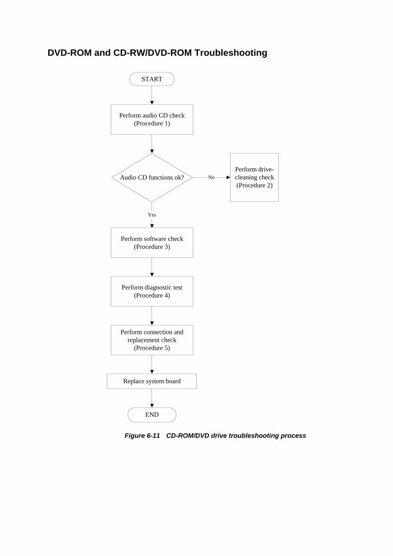
DVD-ROM and CD-RW/DVD-ROM Troubleshooting
START
Audio CD functions ok?
END
Perform software check(Procedure 3)
Perform diagnostic test(Procedure 4)
Perform connection andreplacement check
(Procedure 5)
Perform audio CD check(Procedure 1)
Perform drive-cleaning check(Procedure 2)
No
Yes
Replace system board
Figure 6-11 CD-ROM/DVD drive troubleshooting process
This section describes how to determine if the computer’s internal DVD-ROM drive or CD-RW/DVD-ROM drive is functioning properly. Figure 6-11 outlines the process. Perform the steps below starting with Procedure 1 and continue with the other procedures as required.
Procedure 1: Audio CD test Procedure 2: Drive cleaning check Procedure 3: Software check Procedure 4: Diagnostic test Procedure 5: Connection and replacement check
Procedure 1 Audio CD check
First, insert an audio CD into the CD/DVD drive. If it works, the problem is not with the drive. Go to Procedure 3. If the audio CD does not work, go to Procedure 2. If the CD/DVD LED on the front panel does not light when the disc is played and the drive gives no response, go straight to Procedure 3.
Procedure 2 Drive cleaning check
Insert a CD/DVD drive-cleaning disk into the drive clean according to the drive-cleaning product instructions. If the problem persists, go to Procedure 3.
Procedure 3 Software check
Ensure that the appropriate driver has been installed on the computer for the CD/DVD drive.
Procedure 4 Diagnostic test
The CD-ROM/DVD-ROM test program stored in the Diagnostics Disk will test the drive’s ability to play an audio CD, as well as the functions of the CD control buttons. If any errors occur while executing the diagnostic program, go to Procedure 5.
Procedure 5 Connection check and replacement check
The DVD-ROM drive or the CD-RW/DVD-ROM drive connects to the system board. The drive may be disconnected, or the drive or system board may be damaged. Replacement Procedures and perform the following checks:
Check 1 Make sure the drive is firmly connected to the system board. If the connection is good and there is still an error, go to Check 2.
Check 2 The drive or drive cable may be defective or damaged. Replacement Procedures. If the drive is still not functioning properly, perform Check 3.
Check 3 The system board may be damaged.
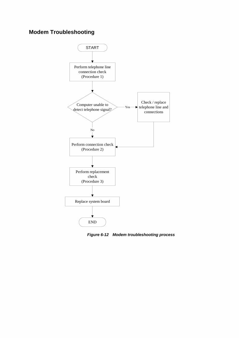
Modem Troubleshooting
START
Computer unable todetect telephone signal?
END
Perform connection check(Procedure 2)
Perform replacementcheck
(Procedure 3)
Perform telephone lineconnection check
(Procedure 1)
Check / replacetelephone line and
connectionsYes
Replace system board
No
Figure 6-12 Modem troubleshooting process
This section describes how to determine if the computer's modem is functioning properly. Figure 6-12 outlines the process. Perform the steps below starting with Procedure 1 and continuing with the other procedures as required.
Procedure 1: Telephone line connection check
Procedure 2: Modem card connection check
Procedure 3: Modem card replacement check
Procedure 1 Telephone line connection check
The telephone cable may be damaged or the connections may be loose. Attempt to connect the computer to a network through using the modem. If the modem does not function at all, go to Procedure 3. If the attempt fails because the computer detects no telephone signal, the fault may be in the telephone cable, the wall socket or the modem port. Perform Check 1:
Check 1 Make sure telephone cable is firmly plugged into both the telephone wall socket and the modem port of the computer. If the cable is connected correctly, go to Check 2.
Check 2 Make sure the modem port is firmly secured to the system board of the computer. If the malfunction remains, go to Check 3.
Check 3 The telephone cable may be damaged. Replace with a good cable. If the malfunction remains, go to Procedure 2
Procedure 2 Modem card connection check
Disassemble the computer following the steps described Replacement Procedures and ensure that the modem card is well connected to the system board. If the problem persists, perform Procedure 3.
Procedure 3 Modem replacement check
The modem card or RJ-11 jack may be faulty. Try replacing them. If the problem persists, the system board may be defective or damaged. Replace the System Board with a new one following the steps Replacement Procedures.
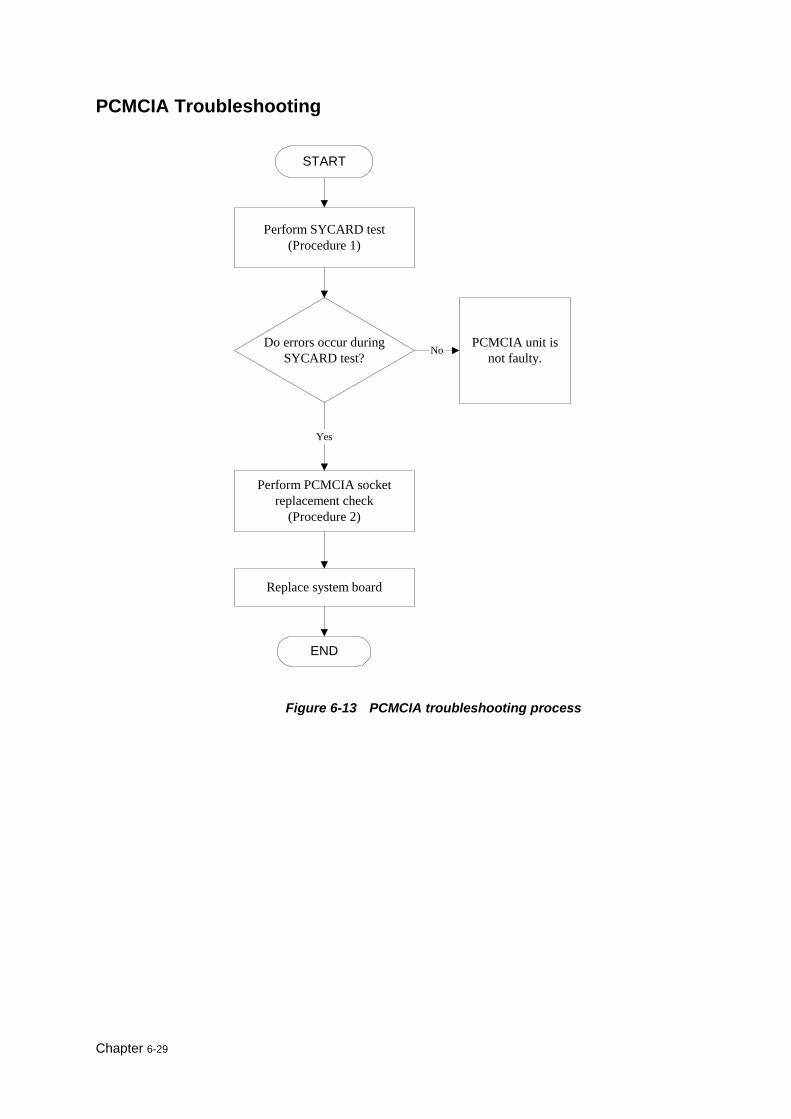
PCMCIA Troubleshooting
START
Do errors occur duringSYCARD test?
Perform PCMCIA socketreplacement check
(Procedure 2)
Replace system board
END
PCMCIA unit isnot faulty.
Perform SYCARD test(Procedure 1)
No
Yes
Figure 6-13 PCMCIA troubleshooting process
Chapter 6-29
This section describes how to determine if the PCMCIA card player is functioning properly. The process is summarized in Figure 6-13. Perform the steps below starting with Procedure 1 and continuing with the other procedures as required.
Procedure 1: Sycard test
Procedure 2: PCMCIA socket replacement check
Procedure 1 SYCARD test
The SYCARD test card contains a PCMCIA test program. Ensure the card in fully inserted into the socket before running the program.
If an error occurs during the SYCARD test, perform Procedure 2. If no error occurs, it is likely the that original PC card was faulty.
Procedure 2 PCMCIA socket replacement check
The PCMCIA socket may be damaged or defective, for instance the socket pins can be bent. Disassemble the computer following the steps described in Chapter 4, Replacement Procedures and replace the socket. If the problem persists, the system board may be defective or damaged.
Chapter 6-30
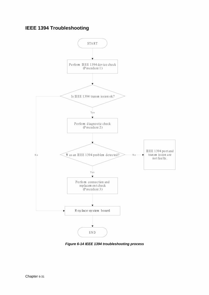
IEEE 1394 Troubleshooting
STA R T
Perform IE E E 1394 device check(Procedure 1)
Is IE EE 1394 transm ission ok?
E N D
Yes
Perform diagnostic check(Procedure 2)
Perform connection and replacem ent check
(Procedure 3)
Yes
IE EE 1394 port and transm ission are
not faulty.N oN o W as an IE EE 1394 problem detected?
Figure 6-14 IEEE 1394 troubleshooting process
Chapter 6-31
To determine if the computer’s IEEE 1394 system is functioning properly, perform the following procedures. Figure 2-14 outlines the process. Start with Procedure 1 and continue with the other procedures as instructed.
Procedure 1: IEEE 1394 device check
Procedure 2: Diagnostic check
Procedure 3: Connection and replacement check
Procedure 1 IEEE 1394 device check
Connect an IEEE 1394 device to the computer’s IEEE 1394 port, then boot the computer for Windows XP. The computer should automatically detect the 1394 device. Check whether the device can transmit data to the computer. If the device is able to communicate with the computer, the problem may be intermittent or connections may be faulty. Go to Procedure 2. If communication is impaired, there may be a faulty connection. Go to Procedure 3.
Procedure 2 Diagnostic check
Run the Diagnostic Program, which will automatically execute the IEEE 1394 port test to test transmission. Refer to Chapter 3, Tests and Diagnostics for more information on how to run the program. If an error is located, go to Procedure 3. If an error does not occur, the 1394 port is functioning properly.
Procedure 3 Connection and replacement check
The transmission cable may be damaged or the connections may be loose. Perform Check 1:
Check 1 Make sure the transmission cable is firmly plugged into both the IEEE 1394-compatible device and the IEEE 1394 port of the computer. If the cable is connected correctly, go to Check 2.
Check 2 Make sure the IEEE 1394 port is firmly secured to the system board of the computer. If the malfunction persists, go to Check 3.
Check 3 The transmission cable may be damaged. Replace with a good cable. If the malfunction persists, go to Check 4.
Check 4 The system board may be damaged. Replace it with a new one following the instructions in Chapter 4.
Chapter 6-32
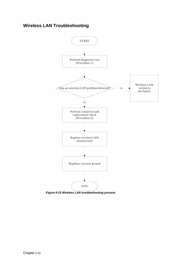
Wireless LAN Troubleshooting
START
Perform diagnostic test(Procedure 1)
Was an wireless LAN problem delected?
Yes
Perform connector and replacement check
(Procedure 2)
END
Wireless LAN system is not faulty.
No
Replace wireless LAN antenna/unit
Figure 6-15 Wireless LAN troubleshooting process
Chapter 6-33
The wireless LAN antenna wire, wireless LAN unit or system board may each be the source of a wireless LAN fault. Any of these components may be damaged. To determine if the computer’s wireless LAN system is functioning properly, perform the following procedures. Figure 2-15 outlines the process. Start with Procedure 1 and continue with the other procedures as instructed.
Procedure 1: Diagnostic test
Procedure 2: Connector and replacement check
Procedure 1 Diagnostic test
Run the Diagnostic Program, which will automatically execute the wireless LAN test. Refer to Chapter 3, Tests and Diagnostics for more information on the program. If an error is located, go to Procedure 2. If an error is not located, the wireless LAN system is functioning properly.
Procedure 2 Connector and replacement check
The wireless LAN antenna, wireless LAN unit or system board may be disconnected or damaged. Disassemble the computer following the steps described in Chapter 4, Replacement Procedures, and perform the following checks. Check 1 Make sure that the wireless LAN antenna is firmly connected to the wireless LAN unit
(refer to Chapter 4 for instructions) and that the wireless LAN unit is securely slotted into the system board. If the problem persists, go to Check 2.
Check 2 Check that the wireless communication switch is turned to “On”, then make sure that the wireless communication LED on the front panel is lit. If the LED is lit but the wireless LAN function is still faulty, the antenna may be damaged. Replace with a new antenna following the steps in Chapter 4, Replacement Procedures. If the problem persists, or if the wireless LAN LED is not lit when the wireless communication switch is turned to “On”, go to Check 3.
Check 3 The wireless LAN unit may be damaged. Replace it with a new one following the instructions in Chapter 4. If the problem still exists, perform Check 4.
Check 4 The system board may be damaged. Replace it with a new one following the instructions in Chapter
Chapter 6-34

Material List by Single-Item/Single-Level
------------------------------------------------------------------------------------------------------------------------------------
Date : 05-07-2002
Time : 11:02:16 Drawing No: ACY25
Plant: TW01 Revision: 1A
Report by UID: 8746109
C NO PART NO DESCRIPTION QUANTITY REQUIRED LOCATION
25D01
------------------------------------------------------------------------------------------------------------------------------------
# ACY25D01 FG 030 14.1" XGA TEST REF - - - -
001 AB805320010 IC RH80532GC021512 B 1.5G UFCPGA 1 001
002 AB805320030 IC RH80532GC021512B0 1.5G FCPGA2 1 001
003 AB805320110 IC RH80532GC025512 B 1.6G UFCPGA 1 001
004 AB805320130 IC RH80532GC025512B0 1.6G FCPGA2 1 001
005 AB805320210 IC RH80532GC017512 B 1.4G UFCPGA 1 001
006 AB805320230 IC RH80532GC017512B0 1.4G FCPGA2 1 001
007 AB805320320 IC RH80532GC013512B0 1.3G FCPGA2 1 001
008 AB805320410 IC RH80532GC029512 B 1.7G UFCPGA 1 001
009 AB805320430 IC RH80532GC029512B0 1.7G FCPGA2 1 001
010 AB805320800 IC TST RH80532GC033512S 1.8PCPGA A31 1 001
011 AB805320810 IC RH80532GC033512B 1.8G UFCPGA 1 001
012 DD100020000 HDD 20G 2.75"W .37"H MK2018GAP 1 002
013 DD100020100 HDD 40G 2.75"W .37"H MK4018GAP 1 002
014 DD100020300 HDD 30G 2.75"W .37"H MK3018GAP 1 002
015 DD100020500 HDD 20G 2.75"W .37"H DK23DA-20F 1 002
016 DD100020600 HDD 30G 2.75"W .37"H DK23DA-30F 1 002
017 DD100020700 HDD 40G 2.75"W .37"H DK23DA-40F 1 002
018 DD100020900 HDD 20G .37"H IC25N020ATCS04-0 1 002
019 DD100021000 HDD 30G .37"H IC25N030ATCS04-0 1 002
020 DD100021100 HDD 40G .37"H IC25N040ATCS04-0 1 002
021 GA020120605 PWR CORD SP021AX1.8MXIS033 H03 BLK 1 003
022 GA020260000 PWR CORD LP21X1.8MXLS7 EC 2P L 1 003
023 GA040060100 PWR CORD LP60LX1.8MXLS7 UK 2P L 1 003
024 GA040100000 PWR CORD SP61*1.8M*IS037 H03 BLK UK 1 003
025 GA050070100 PWR CORD SP12NX1.8MXIS033 SPT-2 BLK 1 003
026 GA050100000 PWR CORD LP5X1.8MXLS7C US 2P L 1 003
027 GA060040009 PWR CORD SP501X1.8MXIS033 2LDF BLK 1 003
028 GA060090000 PWR CORD LP15AX1.8MXLS7 AUS 2P L 1 003
029 GA090020000 PWR CORD SP505X1.8MXIS033 RVV2C BLK 1 003
030 GA090040000 PWR CORD PC205X1.8XCOC03 CHI 2P L 1 003
031 GC86508PA30 BATT CGR18650A LI-ION 3.9AH 30N3 1 004
032 GC86508SM20 BATT ICR18650 LI-ION 3.9AH 30N3 1 004
033 PK100006400 AC ADAP ASTEC SA80-3105-2278 70W 2P 1 005
034 PK100007000 AC ADAP LITEON PA-1750-01CA 75W 2P A30 1 005
035 PK051000340 DDR MODU HYN HYMD116M645A6-H 128M/266 1 006
036 PK051000820 DDR MODU SAM M470L1624BT0-CB0 128M/266 1 006
037 PK051001500 DDR MODU NAN NT128D64S88A2GM-7K 128/266 1 006
038 PK051002000 DDR MODU APACER 77.10921.580 128M/266 1 006
039 PK051020320 DDR MODU SAM M470L3224BT0-CB0 256/266 1 006
040 PK051020820 DDR MODU HYN HYMD232M6466-H 256M/266 1 006
041 PK051021100 DDR MODU NAN NT256D64S88A2GM-7K 256/266 1 006
042 PK051021300 DDR MODU MIT MH32D64KQH-75 256M/266 1 006
043 PK051021700 DDR MODU APACER 77.11021.580 256M/266 1 006
044 PK051030010 DDR MODU SAM M470L6423CK0-CB0 512/266 1 006
045 PK051030500 DDR MODU MIT MH64D64AKQH-75 512M/266 1 006
046 PK13CY250AR K/B PACK CHICONY ACY25 AR-E REV00 A30 1 101
047 PK13CY250BE K/B PACK CHICONY ACY25 BE REV00 A30 1 101
048 PK13CY250CF K/B PACK CHICONY ACY25 CF REV00 A30 1 101
049 PK13CY250CH K/B PACK CHICONY ACY25 CH REV00 A30 1 101
050 PK13CY250CZ K/B PACK CHICONY ACY25 CZ REV00 A30 1 101
051 PK13CY250DM K/B PACK CHICONY ACY25 DM REV00 A30 1 101
A-2
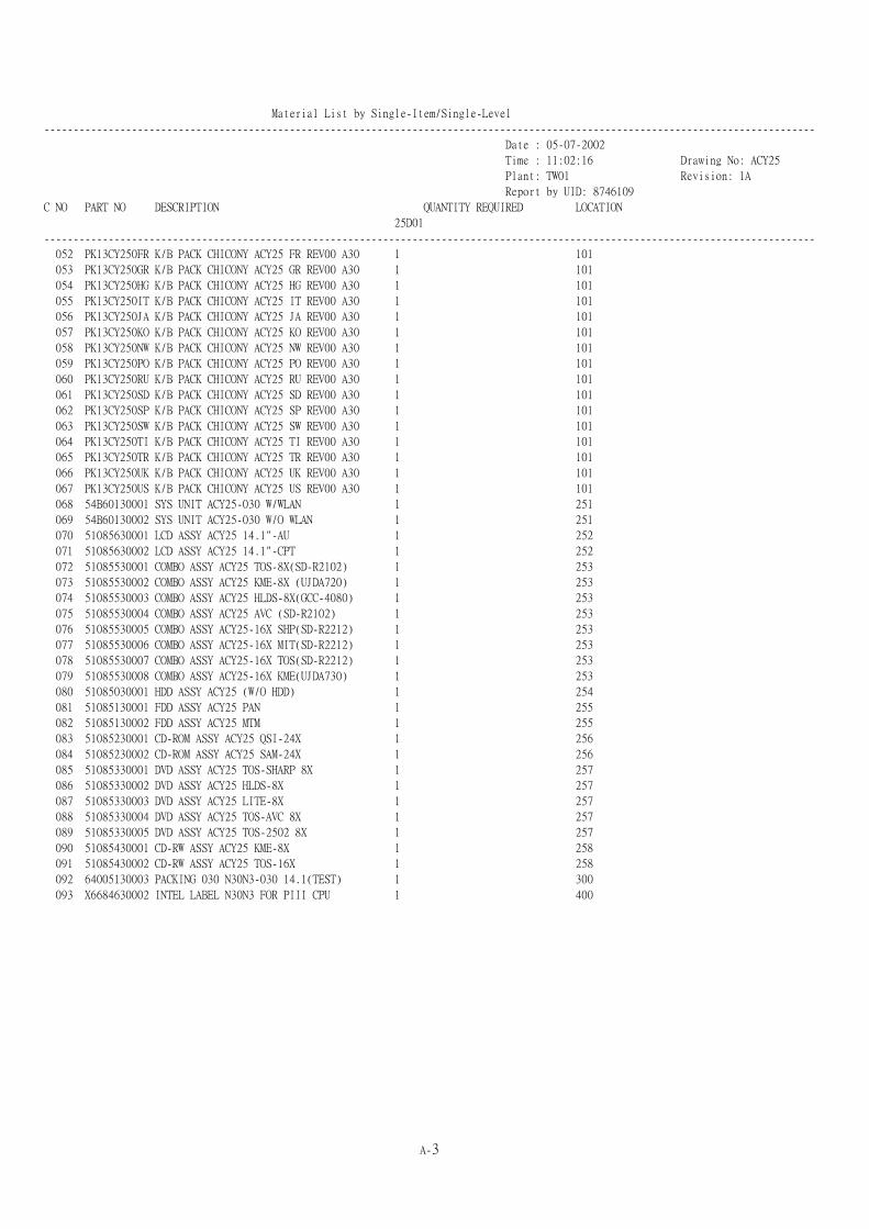
Material List by Single-Item/Single-Level
------------------------------------------------------------------------------------------------------------------------------------
Date : 05-07-2002
Time : 11:02:16 Drawing No: ACY25
Plant: TW01 Revision: 1A
Report by UID: 8746109
C NO PART NO DESCRIPTION QUANTITY REQUIRED LOCATION
25D01
------------------------------------------------------------------------------------------------------------------------------------
052 PK13CY250FR K/B PACK CHICONY ACY25 FR REV00 A30 1 101
053 PK13CY250GR K/B PACK CHICONY ACY25 GR REV00 A30 1 101
054 PK13CY250HG K/B PACK CHICONY ACY25 HG REV00 A30 1 101
055 PK13CY250IT K/B PACK CHICONY ACY25 IT REV00 A30 1 101
056 PK13CY250JA K/B PACK CHICONY ACY25 JA REV00 A30 1 101
057 PK13CY250KO K/B PACK CHICONY ACY25 KO REV00 A30 1 101
058 PK13CY250NW K/B PACK CHICONY ACY25 NW REV00 A30 1 101
059 PK13CY250PO K/B PACK CHICONY ACY25 PO REV00 A30 1 101
060 PK13CY250RU K/B PACK CHICONY ACY25 RU REV00 A30 1 101
061 PK13CY250SD K/B PACK CHICONY ACY25 SD REV00 A30 1 101
062 PK13CY250SP K/B PACK CHICONY ACY25 SP REV00 A30 1 101
063 PK13CY250SW K/B PACK CHICONY ACY25 SW REV00 A30 1 101
064 PK13CY250TI K/B PACK CHICONY ACY25 TI REV00 A30 1 101
065 PK13CY250TR K/B PACK CHICONY ACY25 TR REV00 A30 1 101
066 PK13CY250UK K/B PACK CHICONY ACY25 UK REV00 A30 1 101
067 PK13CY250US K/B PACK CHICONY ACY25 US REV00 A30 1 101
068 54B60130001 SYS UNIT ACY25-030 W/WLAN 1 251
069 54B60130002 SYS UNIT ACY25-030 W/O WLAN 1 251
070 51085630001 LCD ASSY ACY25 14.1"-AU 1 252
071 51085630002 LCD ASSY ACY25 14.1"-CPT 1 252
072 51085530001 COMBO ASSY ACY25 TOS-8X(SD-R2102) 1 253
073 51085530002 COMBO ASSY ACY25 KME-8X (UJDA720) 1 253
074 51085530003 COMBO ASSY ACY25 HLDS-8X(GCC-4080) 1 253
075 51085530004 COMBO ASSY ACY25 AVC (SD-R2102) 1 253
076 51085530005 COMBO ASSY ACY25-16X SHP(SD-R2212) 1 253
077 51085530006 COMBO ASSY ACY25-16X MIT(SD-R2212) 1 253
078 51085530007 COMBO ASSY ACY25-16X TOS(SD-R2212) 1 253
079 51085530008 COMBO ASSY ACY25-16X KME(UJDA730) 1 253
080 51085030001 HDD ASSY ACY25 (W/O HDD) 1 254
081 51085130001 FDD ASSY ACY25 PAN 1 255
082 51085130002 FDD ASSY ACY25 MTM 1 255
083 51085230001 CD-ROM ASSY ACY25 QSI-24X 1 256
084 51085230002 CD-ROM ASSY ACY25 SAM-24X 1 256
085 51085330001 DVD ASSY ACY25 TOS-SHARP 8X 1 257
086 51085330002 DVD ASSY ACY25 HLDS-8X 1 257
087 51085330003 DVD ASSY ACY25 LITE-8X 1 257
088 51085330004 DVD ASSY ACY25 TOS-AVC 8X 1 257
089 51085330005 DVD ASSY ACY25 TOS-2502 8X 1 257
090 51085430001 CD-RW ASSY ACY25 KME-8X 1 258
091 51085430002 CD-RW ASSY ACY25 TOS-16X 1 258
092 64005130003 PACKING 030 N30N3-030 14.1(TEST) 1 300
093 X6684630002 INTEL LABEL N30N3 FOR PIII CPU 1 400
A-3
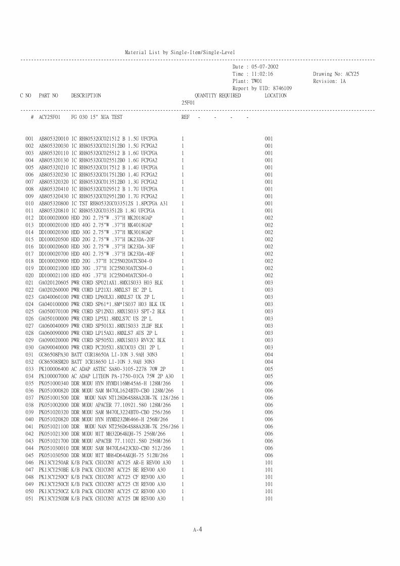
Material List by Single-Item/Single-Level
------------------------------------------------------------------------------------------------------------------------------------
Date : 05-07-2002
Time : 11:02:16 Drawing No: ACY25
Plant: TW01 Revision: 1A
Report by UID: 8746109
C NO PART NO DESCRIPTION QUANTITY REQUIRED LOCATION
25F01
------------------------------------------------------------------------------------------------------------------------------------
# ACY25F01 FG 030 15" XGA TEST REF - - - -
001 AB805320010 IC RH80532GC021512 B 1.5G UFCPGA 1 001
002 AB805320030 IC RH80532GC021512B0 1.5G FCPGA2 1 001
003 AB805320110 IC RH80532GC025512 B 1.6G UFCPGA 1 001
004 AB805320130 IC RH80532GC025512B0 1.6G FCPGA2 1 001
005 AB805320210 IC RH80532GC017512 B 1.4G UFCPGA 1 001
006 AB805320230 IC RH80532GC017512B0 1.4G FCPGA2 1 001
007 AB805320320 IC RH80532GC013512B0 1.3G FCPGA2 1 001
008 AB805320410 IC RH80532GC029512 B 1.7G UFCPGA 1 001
009 AB805320430 IC RH80532GC029512B0 1.7G FCPGA2 1 001
010 AB805320800 IC TST RH80532GC033512S 1.8PCPGA A31 1 001
011 AB805320810 IC RH80532GC033512B 1.8G UFCPGA 1 001
012 DD100020000 HDD 20G 2.75"W .37"H MK2018GAP 1 002
013 DD100020100 HDD 40G 2.75"W .37"H MK4018GAP 1 002
014 DD100020300 HDD 30G 2.75"W .37"H MK3018GAP 1 002
015 DD100020500 HDD 20G 2.75"W .37"H DK23DA-20F 1 002
016 DD100020600 HDD 30G 2.75"W .37"H DK23DA-30F 1 002
017 DD100020700 HDD 40G 2.75"W .37"H DK23DA-40F 1 002
018 DD100020900 HDD 20G .37"H IC25N020ATCS04-0 1 002
019 DD100021000 HDD 30G .37"H IC25N030ATCS04-0 1 002
020 DD100021100 HDD 40G .37"H IC25N040ATCS04-0 1 002
021 GA020120605 PWR CORD SP021AX1.8MXIS033 H03 BLK 1 003
022 GA020260000 PWR CORD LP21X1.8MXLS7 EC 2P L 1 003
023 GA040060100 PWR CORD LP60LX1.8MXLS7 UK 2P L 1 003
024 GA040100000 PWR CORD SP61*1.8M*IS037 H03 BLK UK 1 003
025 GA050070100 PWR CORD SP12NX1.8MXIS033 SPT-2 BLK 1 003
026 GA050100000 PWR CORD LP5X1.8MXLS7C US 2P L 1 003
027 GA060040009 PWR CORD SP501X1.8MXIS033 2LDF BLK 1 003
028 GA060090000 PWR CORD LP15AX1.8MXLS7 AUS 2P L 1 003
029 GA090020000 PWR CORD SP505X1.8MXIS033 RVV2C BLK 1 003
030 GA090040000 PWR CORD PC205X1.8XCOC03 CHI 2P L 1 003
031 GC86508PA30 BATT CGR18650A LI-ION 3.9AH 30N3 1 004
032 GC86508SM20 BATT ICR18650 LI-ION 3.9AH 30N3 1 004
033 PK100006400 AC ADAP ASTEC SA80-3105-2278 70W 2P 1 005
034 PK100007000 AC ADAP LITEON PA-1750-01CA 75W 2P A30 1 005
035 PK051000340 DDR MODU HYN HYMD116M645A6-H 128M/266 1 006
036 PK051000820 DDR MODU SAM M470L1624BT0-CB0 128M/266 1 006
037 PK051001500 DDR MODU NAN NT128D64S88A2GM-7K 128/266 1 006
038 PK051002000 DDR MODU APACER 77.10921.580 128M/266 1 006
039 PK051020320 DDR MODU SAM M470L3224BT0-CB0 256/266 1 006
040 PK051020820 DDR MODU HYN HYMD232M6466-H 256M/266 1 006
041 PK051021100 DDR MODU NAN NT256D64S88A2GM-7K 256/266 1 006
042 PK051021300 DDR MODU MIT MH32D64KQH-75 256M/266 1 006
043 PK051021700 DDR MODU APACER 77.11021.580 256M/266 1 006
044 PK051030010 DDR MODU SAM M470L6423CK0-CB0 512/266 1 006
045 PK051030500 DDR MODU MIT MH64D64AKQH-75 512M/266 1 006
046 PK13CY250AR K/B PACK CHICONY ACY25 AR-E REV00 A30 1 101
047 PK13CY250BE K/B PACK CHICONY ACY25 BE REV00 A30 1 101
048 PK13CY250CF K/B PACK CHICONY ACY25 CF REV00 A30 1 101
049 PK13CY250CH K/B PACK CHICONY ACY25 CH REV00 A30 1 101
050 PK13CY250CZ K/B PACK CHICONY ACY25 CZ REV00 A30 1 101
051 PK13CY250DM K/B PACK CHICONY ACY25 DM REV00 A30 1 101
A-4
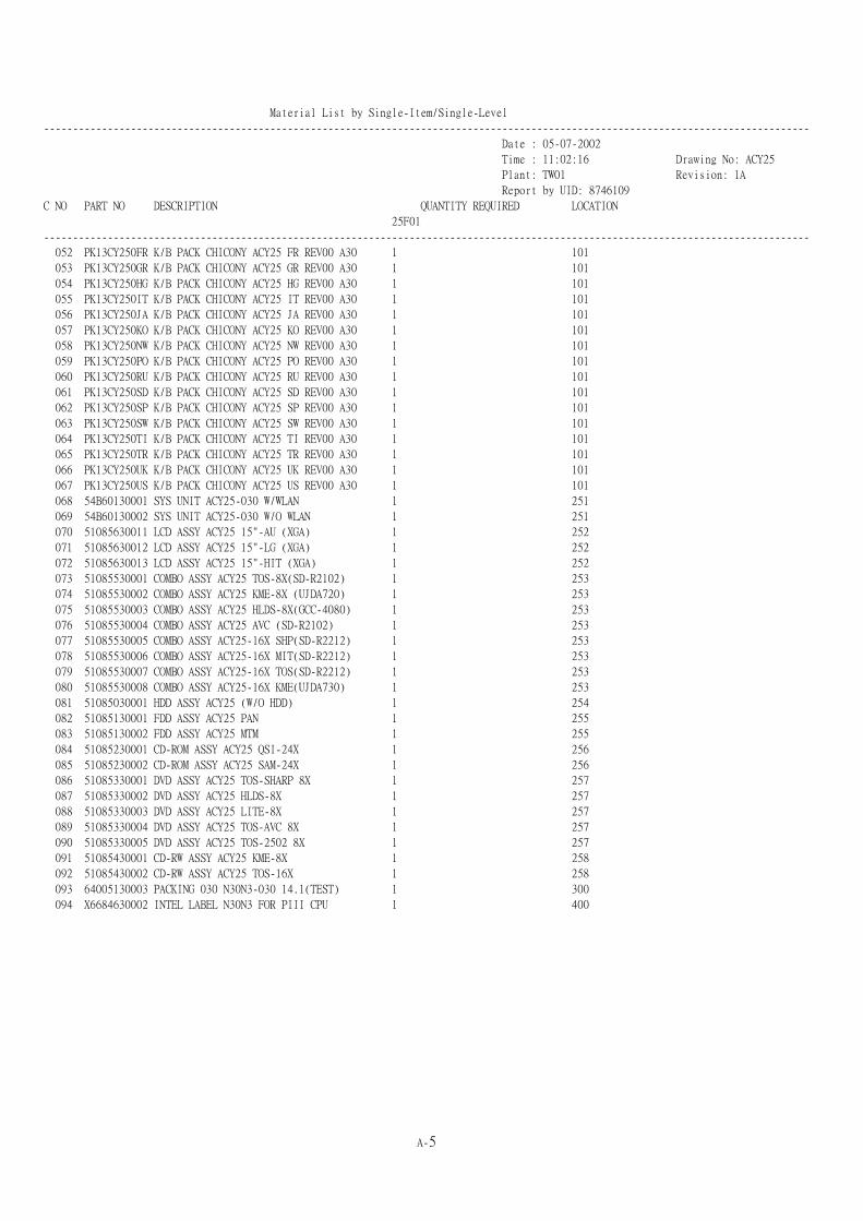
Material List by Single-Item/Single-Level
------------------------------------------------------------------------------------------------------------------------------------
Date : 05-07-2002
Time : 11:02:16 Drawing No: ACY25
Plant: TW01 Revision: 1A
Report by UID: 8746109
C NO PART NO DESCRIPTION QUANTITY REQUIRED LOCATION
25F01
------------------------------------------------------------------------------------------------------------------------------------
052 PK13CY250FR K/B PACK CHICONY ACY25 FR REV00 A30 1 101
053 PK13CY250GR K/B PACK CHICONY ACY25 GR REV00 A30 1 101
054 PK13CY250HG K/B PACK CHICONY ACY25 HG REV00 A30 1 101
055 PK13CY250IT K/B PACK CHICONY ACY25 IT REV00 A30 1 101
056 PK13CY250JA K/B PACK CHICONY ACY25 JA REV00 A30 1 101
057 PK13CY250KO K/B PACK CHICONY ACY25 KO REV00 A30 1 101
058 PK13CY250NW K/B PACK CHICONY ACY25 NW REV00 A30 1 101
059 PK13CY250PO K/B PACK CHICONY ACY25 PO REV00 A30 1 101
060 PK13CY250RU K/B PACK CHICONY ACY25 RU REV00 A30 1 101
061 PK13CY250SD K/B PACK CHICONY ACY25 SD REV00 A30 1 101
062 PK13CY250SP K/B PACK CHICONY ACY25 SP REV00 A30 1 101
063 PK13CY250SW K/B PACK CHICONY ACY25 SW REV00 A30 1 101
064 PK13CY250TI K/B PACK CHICONY ACY25 TI REV00 A30 1 101
065 PK13CY250TR K/B PACK CHICONY ACY25 TR REV00 A30 1 101
066 PK13CY250UK K/B PACK CHICONY ACY25 UK REV00 A30 1 101
067 PK13CY250US K/B PACK CHICONY ACY25 US REV00 A30 1 101
068 54B60130001 SYS UNIT ACY25-030 W/WLAN 1 251
069 54B60130002 SYS UNIT ACY25-030 W/O WLAN 1 251
070 51085630011 LCD ASSY ACY25 15"-AU (XGA) 1 252
071 51085630012 LCD ASSY ACY25 15"-LG (XGA) 1 252
072 51085630013 LCD ASSY ACY25 15"-HIT (XGA) 1 252
073 51085530001 COMBO ASSY ACY25 TOS-8X(SD-R2102) 1 253
074 51085530002 COMBO ASSY ACY25 KME-8X (UJDA720) 1 253
075 51085530003 COMBO ASSY ACY25 HLDS-8X(GCC-4080) 1 253
076 51085530004 COMBO ASSY ACY25 AVC (SD-R2102) 1 253
077 51085530005 COMBO ASSY ACY25-16X SHP(SD-R2212) 1 253
078 51085530006 COMBO ASSY ACY25-16X MIT(SD-R2212) 1 253
079 51085530007 COMBO ASSY ACY25-16X TOS(SD-R2212) 1 253
080 51085530008 COMBO ASSY ACY25-16X KME(UJDA730) 1 253
081 51085030001 HDD ASSY ACY25 (W/O HDD) 1 254
082 51085130001 FDD ASSY ACY25 PAN 1 255
083 51085130002 FDD ASSY ACY25 MTM 1 255
084 51085230001 CD-ROM ASSY ACY25 QSI-24X 1 256
085 51085230002 CD-ROM ASSY ACY25 SAM-24X 1 256
086 51085330001 DVD ASSY ACY25 TOS-SHARP 8X 1 257
087 51085330002 DVD ASSY ACY25 HLDS-8X 1 257
088 51085330003 DVD ASSY ACY25 LITE-8X 1 257
089 51085330004 DVD ASSY ACY25 TOS-AVC 8X 1 257
090 51085330005 DVD ASSY ACY25 TOS-2502 8X 1 257
091 51085430001 CD-RW ASSY ACY25 KME-8X 1 258
092 51085430002 CD-RW ASSY ACY25 TOS-16X 1 258
093 64005130003 PACKING 030 N30N3-030 14.1(TEST) 1 300
094 X6684630002 INTEL LABEL N30N3 FOR PIII CPU 1 400
A-5

Material List by Single-Item/Single-Level
------------------------------------------------------------------------------------------------------------------------------------
Date : 05-07-2002
Time : 11:02:16 Drawing No: ACY25
Plant: TW01 Revision: 1A
Report by UID: 8746109
C NO PART NO DESCRIPTION QUANTITY REQUIRED LOCATION
25G01
------------------------------------------------------------------------------------------------------------------------------------
# ACY25G01 FG 030 15" SXGA TEST REF - - - -
001 AB805320010 IC RH80532GC021512 B 1.5G UFCPGA 1 001
002 AB805320030 IC RH80532GC021512B0 1.5G FCPGA2 1 001
003 AB805320110 IC RH80532GC025512 B 1.6G UFCPGA 1 001
004 AB805320130 IC RH80532GC025512B0 1.6G FCPGA2 1 001
005 AB805320210 IC RH80532GC017512 B 1.4G UFCPGA 1 001
006 AB805320230 IC RH80532GC017512B0 1.4G FCPGA2 1 001
007 AB805320320 IC RH80532GC013512B0 1.3G FCPGA2 1 001
008 AB805320410 IC RH80532GC029512 B 1.7G UFCPGA 1 001
009 AB805320430 IC RH80532GC029512B0 1.7G FCPGA2 1 001
010 AB805320800 IC TST RH80532GC033512S 1.8PCPGA A31 1 001
011 AB805320810 IC RH80532GC033512B 1.8G UFCPGA 1 001
012 DD100020000 HDD 20G 2.75"W .37"H MK2018GAP 1 002
013 DD100020100 HDD 40G 2.75"W .37"H MK4018GAP 1 002
014 DD100020300 HDD 30G 2.75"W .37"H MK3018GAP 1 002
015 DD100020500 HDD 20G 2.75"W .37"H DK23DA-20F 1 002
016 DD100020600 HDD 30G 2.75"W .37"H DK23DA-30F 1 002
017 DD100020700 HDD 40G 2.75"W .37"H DK23DA-40F 1 002
018 DD100020900 HDD 20G .37"H IC25N020ATCS04-0 1 002
019 DD100021000 HDD 30G .37"H IC25N030ATCS04-0 1 002
020 DD100021100 HDD 40G .37"H IC25N040ATCS04-0 1 002
021 GA020120605 PWR CORD SP021AX1.8MXIS033 H03 BLK 1 003
022 GA020260000 PWR CORD LP21X1.8MXLS7 EC 2P L 1 003
023 GA040060100 PWR CORD LP60LX1.8MXLS7 UK 2P L 1 003
024 GA040100000 PWR CORD SP61*1.8M*IS037 H03 BLK UK 1 003
025 GA050070100 PWR CORD SP12NX1.8MXIS033 SPT-2 BLK 1 003
026 GA050100000 PWR CORD LP5X1.8MXLS7C US 2P L 1 003
027 GA060040009 PWR CORD SP501X1.8MXIS033 2LDF BLK 1 003
028 GA060090000 PWR CORD LP15AX1.8MXLS7 AUS 2P L 1 003
029 GA090020000 PWR CORD SP505X1.8MXIS033 RVV2C BLK 1 003
030 GA090040000 PWR CORD PC205X1.8XCOC03 CHI 2P L 1 003
031 GC86508PA30 BATT CGR18650A LI-ION 3.9AH 30N3 1 004
032 GC86508SM20 BATT ICR18650 LI-ION 3.9AH 30N3 1 004
033 PK100006400 AC ADAP ASTEC SA80-3105-2278 70W 2P 1 005
034 PK100007000 AC ADAP LITEON PA-1750-01CA 75W 2P A30 1 005
035 PK051000340 DDR MODU HYN HYMD116M645A6-H 128M/266 1 006
036 PK051000820 DDR MODU SAM M470L1624BT0-CB0 128M/266 1 006
037 PK051001500 DDR MODU NAN NT128D64S88A2GM-7K 128/266 1 006
038 PK051002000 DDR MODU APACER 77.10921.580 128M/266 1 006
039 PK051020320 DDR MODU SAM M470L3224BT0-CB0 256/266 1 006
040 PK051020820 DDR MODU HYN HYMD232M6466-H 256M/266 1 006
041 PK051021100 DDR MODU NAN NT256D64S88A2GM-7K 256/266 1 006
042 PK051021300 DDR MODU MIT MH32D64KQH-75 256M/266 1 006
043 PK051021700 DDR MODU APACER 77.11021.580 256M/266 1 006
044 PK051030010 DDR MODU SAM M470L6423CK0-CB0 512/266 1 006
045 PK051030500 DDR MODU MIT MH64D64AKQH-75 512M/266 1 006
046 PK13CY250AR K/B PACK CHICONY ACY25 AR-E REV00 A30 1 101
047 PK13CY250BE K/B PACK CHICONY ACY25 BE REV00 A30 1 101
048 PK13CY250CF K/B PACK CHICONY ACY25 CF REV00 A30 1 101
049 PK13CY250CH K/B PACK CHICONY ACY25 CH REV00 A30 1 101
050 PK13CY250CZ K/B PACK CHICONY ACY25 CZ REV00 A30 1 101
051 PK13CY250DM K/B PACK CHICONY ACY25 DM REV00 A30 1 101
A-6

Material List by Single-Item/Single-Level
------------------------------------------------------------------------------------------------------------------------------------
Date : 05-07-2002
Time : 11:02:16 Drawing No: ACY25
Plant: TW01 Revision: 1A
Report by UID: 8746109
C NO PART NO DESCRIPTION QUANTITY REQUIRED LOCATION
25G01
------------------------------------------------------------------------------------------------------------------------------------
052 PK13CY250FR K/B PACK CHICONY ACY25 FR REV00 A30 1 101
053 PK13CY250GR K/B PACK CHICONY ACY25 GR REV00 A30 1 101
054 PK13CY250HG K/B PACK CHICONY ACY25 HG REV00 A30 1 101
055 PK13CY250IT K/B PACK CHICONY ACY25 IT REV00 A30 1 101
056 PK13CY250JA K/B PACK CHICONY ACY25 JA REV00 A30 1 101
057 PK13CY250KO K/B PACK CHICONY ACY25 KO REV00 A30 1 101
058 PK13CY250NW K/B PACK CHICONY ACY25 NW REV00 A30 1 101
059 PK13CY250PO K/B PACK CHICONY ACY25 PO REV00 A30 1 101
060 PK13CY250RU K/B PACK CHICONY ACY25 RU REV00 A30 1 101
061 PK13CY250SD K/B PACK CHICONY ACY25 SD REV00 A30 1 101
062 PK13CY250SP K/B PACK CHICONY ACY25 SP REV00 A30 1 101
063 PK13CY250SW K/B PACK CHICONY ACY25 SW REV00 A30 1 101
064 PK13CY250TI K/B PACK CHICONY ACY25 TI REV00 A30 1 101
065 PK13CY250TR K/B PACK CHICONY ACY25 TR REV00 A30 1 101
066 PK13CY250UK K/B PACK CHICONY ACY25 UK REV00 A30 1 101
067 PK13CY250US K/B PACK CHICONY ACY25 US REV00 A30 1 101
068 54B60130001 SYS UNIT ACY25-030 W/WLAN 1 251
069 54B60130002 SYS UNIT ACY25-030 W/O WLAN 1 251
070 51085630021 LCD ASSY ACY25 15"-CPT (SXGA) 1 252
071 51085630022 LCD ASSY ACY25 15"-LG (SXGA) 1 252
072 51085630023 LCD ASSY ACY25 15"-IBM (SXGA) 1 252
073 51085530001 COMBO ASSY ACY25 TOS-8X(SD-R2102) 1 253
074 51085530002 COMBO ASSY ACY25 KME-8X (UJDA720) 1 253
075 51085530003 COMBO ASSY ACY25 HLDS-8X(GCC-4080) 1 253
076 51085530004 COMBO ASSY ACY25 AVC (SD-R2102) 1 253
077 51085530005 COMBO ASSY ACY25-16X SHP(SD-R2212) 1 253
078 51085530006 COMBO ASSY ACY25-16X MIT(SD-R2212) 1 253
079 51085530007 COMBO ASSY ACY25-16X TOS(SD-R2212) 1 253
080 51085530008 COMBO ASSY ACY25-16X KME(UJDA730) 1 253
081 51085030001 HDD ASSY ACY25 (W/O HDD) 1 254
082 51085130001 FDD ASSY ACY25 PAN 1 255
083 51085130002 FDD ASSY ACY25 MTM 1 255
084 51085230001 CD-ROM ASSY ACY25 QSI-24X 1 256
085 51085230002 CD-ROM ASSY ACY25 SAM-24X 1 256
086 51085330001 DVD ASSY ACY25 TOS-SHARP 8X 1 257
087 51085330002 DVD ASSY ACY25 HLDS-8X 1 257
088 51085330003 DVD ASSY ACY25 LITE-8X 1 257
089 51085330004 DVD ASSY ACY25 TOS-AVC 8X 1 257
090 51085330005 DVD ASSY ACY25 TOS-2502 8X 1 257
091 51085430001 CD-RW ASSY ACY25 KME-8X 1 258
092 51085430002 CD-RW ASSY ACY25 TOS-16X 1 258
093 64005130003 PACKING 030 N30N3-030 14.1(TEST) 1 300
094 X6684630002 INTEL LABEL N30N3 FOR PIII CPU 1 400
END OF REPORT
A-7

Material List by Single-Item/Single-Level
------------------------------------------------------------------------------------------------------------------------------------
Date : 05-02-2002
Time : 15:12:42 Drawing No: 510850
Plant: TW01 Revision: 1A
Report by UID: 8746109
C NO PART NO DESCRIPTION QUANTITY REQUIRED LOCATION
30001
------------------------------------------------------------------------------------------------------------------------------------
# 51085030001 HDD ASSY ACY25 (W/O HDD) REF - - - -
001 MAAA4303000 SCREW M3.0X0.8+3K-NL 4 001
002 EECY2538100 ACY25 HDD BRK COVER 1 002
003 APCY257T100 ACY25_HDD_DOOR_ASSY 1 003
004 DC040011210 SOCKET CONN. AFH-22SD2 44P OCTEKCONN 1 010
END OF REPORT
A-8

Material List by Single-Item/Single-Level
------------------------------------------------------------------------------------------------------------------------------------
Date : 05-07-2002
Time : 08:43:09 Drawing No: 510851
Plant: TW01 Revision: 1B
Report by UID: 8746109
C NO PART NO DESCRIPTION QUANTITY REQUIRED LOCATION
30001 30002
------------------------------------------------------------------------------------------------------------------------------------
# 51085130001 FDD ASSY ACY25 PAN REF - - - -
# 51085130002 FDD ASSY ACY25 MTM - REF - - -
001 MAAA0203000 SCREW M2.0X0.4+3K-ZK - 4 001
002 MAC925003Z0 SCREW M2.5_9_5.5*0.8_03_R00 3 - 001
003 FACY2532100 ACY25 FDD PANEL MIM - 1 002
004 FACY2534100 ACY25 FDD PANEL PASC 1 - 002
005 ECCY2533100 ACY25 FDD BRK MIM - 1 003
006 ECCY2535100 ACY25 FDD BRK PASC 1 - 003
007 MAAA0203000 SCREW M2.0X0.4+3K-ZK 1 - 004
* 008 DA3CY25L010 FPC ACY25 LF-1344 REV1 PANNAS.FDD 1 - 010
* 009 DA3CY25L110 FPC ACY25 LF-1345 REV1 MITSUMI FDD - 1 010
010 DD000005140 FDD 1.44M 4"W .5"H JU-226A273FC 1 - 011
011 DD000005220 FDD 1.44M 4"W .5"H D353G-2938 - 1 011
END OF REPORT
A-9
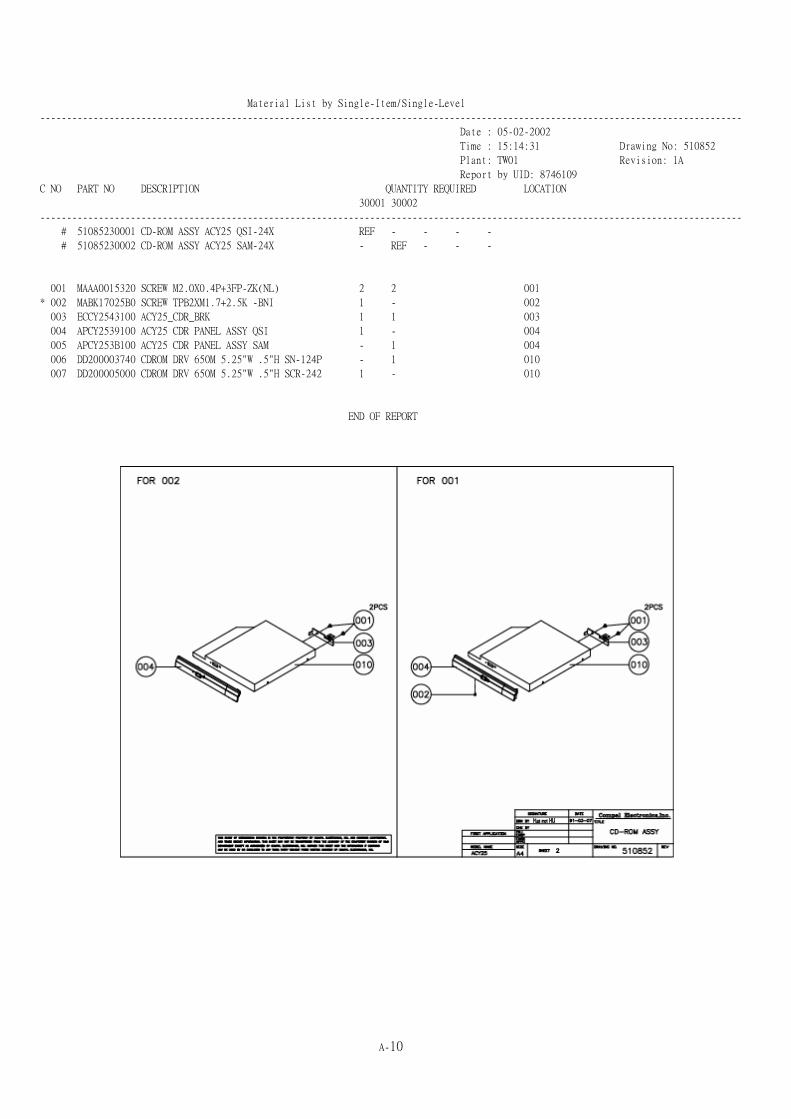
Material List by Single-Item/Single-Level
------------------------------------------------------------------------------------------------------------------------------------
Date : 05-02-2002
Time : 15:14:31 Drawing No: 510852
Plant: TW01 Revision: 1A
Report by UID: 8746109
C NO PART NO DESCRIPTION QUANTITY REQUIRED LOCATION
30001 30002
------------------------------------------------------------------------------------------------------------------------------------
# 51085230001 CD-ROM ASSY ACY25 QSI-24X REF - - - -
# 51085230002 CD-ROM ASSY ACY25 SAM-24X - REF - - -
001 MAAA0015320 SCREW M2.0X0.4P+3FP-ZK(NL) 2 2 001
* 002 MABK17025B0 SCREW TPB2XM1.7+2.5K -BNI 1 - 002
003 ECCY2543100 ACY25_CDR_BRK 1 1 003
004 APCY2539100 ACY25 CDR PANEL ASSY QSI 1 - 004
005 APCY253B100 ACY25 CDR PANEL ASSY SAM - 1 004
006 DD200003740 CDROM DRV 650M 5.25"W .5"H SN-124P - 1 010
007 DD200005000 CDROM DRV 650M 5.25"W .5"H SCR-242 1 - 010
END OF REPORT
A-10
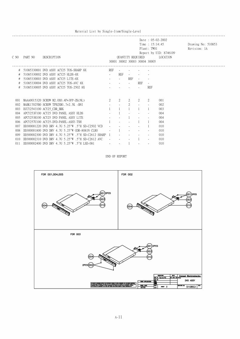
Material List by Single-Item/Single-Level
------------------------------------------------------------------------------------------------------------------------------------
Date : 05-02-2002
Time : 15:14:45 Drawing No: 510853
Plant: TW01 Revision: 1A
Report by UID: 8746109
C NO PART NO DESCRIPTION QUANTITY REQUIRED LOCATION
30001 30002 30003 30004 30005
------------------------------------------------------------------------------------------------------------------------------------
# 51085330001 DVD ASSY ACY25 TOS-SHARP 8X REF - - - -
# 51085330002 DVD ASSY ACY25 HLDS-8X - REF - - -
# 51085330003 DVD ASSY ACY25 LITE-8X - - REF - -
# 51085330004 DVD ASSY ACY25 TOS-AVC 8X - - - REF -
# 51085330005 DVD ASSY ACY25 TOS-2502 8X - - - - REF
001 MAAA0015320 SCREW M2.0X0.4P+3FP-ZK(NL) 2 2 2 2 2 001
002 MABK17025B0 SCREW TPB2XM1.7+2.5K -BNI - - 2 - - 002
003 ECCY2543100 ACY25_CDR_BRK 1 1 1 1 1 003
004 APCY253F100 ACY25 DVD PANEL ASSY HLDS - 1 - - - 004
005 APCY253H100 ACY25 DVD PANEL ASSY LITE - - 1 - - 004
006 APCY257U100 ACY25-DVD-PANEL-ASSY-TSH 1 - - 1 1 004
007 DD300001220 DVD DRV 4.7G 5.25"W .5"H SD-C2502 VCD - - - - 1 010
008 DD300001800 DVD DRV 4.7G 5.25"W GDR-8081N CLBO - 1 - - - 010
009 DD300002300 DVD DRV 4.7G 5.25"W .5"H SD-C2612 SHARP 1 - - - - 010
010 DD300002310 DVD DRV 4.7G 5.25"W .5"H SD-C2612 AVC - - - 1 - 010
011 DD300002400 DVD DRV 4.7G 5.25"W .5"H LSD-081 - - 1 - - 010
END OF REPORT
A-11
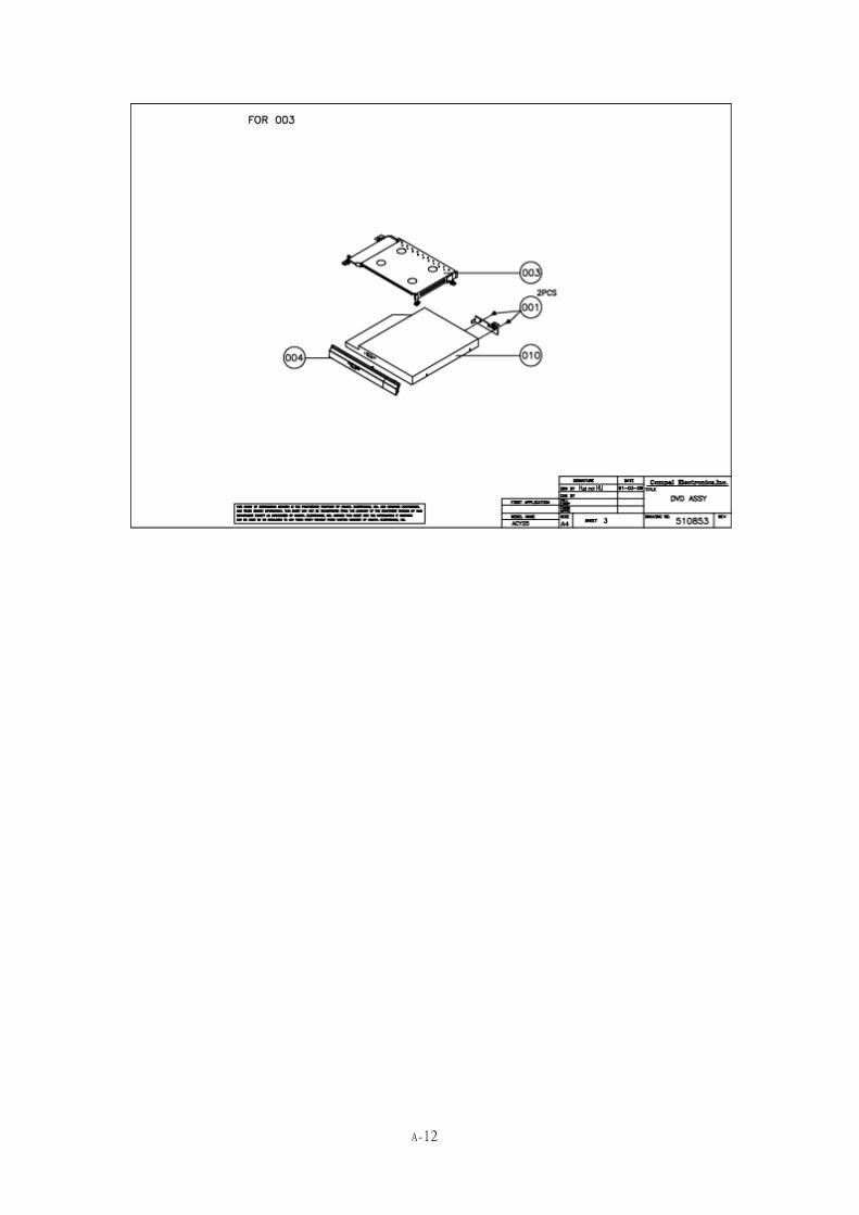
A-12
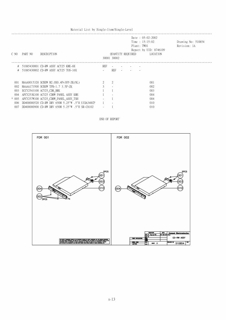
Material List by Single-Item/Single-Level
------------------------------------------------------------------------------------------------------------------------------------
Date : 05-02-2002
Time : 15:15:02 Drawing No: 510854
Plant: TW01 Revision: 1A
Report by UID: 8746109
C NO PART NO DESCRIPTION QUANTITY REQUIRED LOCATION
30001 30002
------------------------------------------------------------------------------------------------------------------------------------
# 51085430001 CD-RW ASSY ACY25 KME-8X REF - - - -
# 51085430002 CD-RW ASSY ACY25 TOS-16X - REF - - -
001 MAAA0015320 SCREW M2.0X0.4P+3FP-ZK(NL) 2 2 001
002 MAAAA173500 SCREW TPB-1.7 3.5P-ZK 3 - 002
003 ECCY2543100 ACY25_CDR_BRK 1 1 003
004 APCY253K100 ACY25 CDRW PANEL ASSY KME 1 - 004
* 005 APCY257W100 ACY25_CDRW_PANEL_ASSY_TSH - 1 004
006 DD400000520 CD-RW DRV 650M 5.25"W .5"H UJDA340CP 1 - 010
007 DD400000900 CD-RW DRV 650M 5.25"W .5"H SR-C8102 - 1 010
END OF REPORT
A-13
Material List by Single-Item/Single-Level
------------------------------------------------------------------------------------------------------------------------------------
Date : 05-02-2002
Time : 15:15:16 Drawing No: 510855
Plant: TW01 Revision: 1A
Report by UID: 8746109
C NO PART NO DESCRIPTION QUANTITY REQUIRED LOCATION
30001 30002 30003 30004 30005
------------------------------------------------------------------------------------------------------------------------------------
# 51085530001 COMBO ASSY ACY25 TOS-8X(SD-R2102) REF - - - -
# 51085530002 COMBO ASSY ACY25 KME-8X (UJDA720) - REF - - -
# 51085530003 COMBO ASSY ACY25 HLDS-8X(GCC-4080) - - REF - -
# 51085530004 COMBO ASSY ACY25 AVC (SD-R2102) - - - REF -
# 51085530005 COMBO ASSY ACY25-16X SHP(SD-R2212) - - - - REF
001 MAAA0015320 SCREW M2.0X0.4P+3FP-ZK(NL) 2 2 2 2 2 001
002 MAAAA173500 SCREW TPB-1.7 3.5P-ZK - 3 - - - 002
003 ECCY2543100 ACY25_CDR_BRK 1 1 1 1 1 003
004 APCY253D100 ACY25 DRDRW PANEL ASSY TSH 1 - - 1 1 004
005 APCY253N100 ACY25 DVDRW PANEL ASSY KME - 1 - - - 004
006 APCY253Q100 ACY25 DVDRW PANEL ASSY HLDS - - 1 - - 004
007 DD5000002C0 COMBO DRV 650/4.7 35"H SD-R2102 1016 1 - - - - 010
008 DD5000002D0 COMBO DRV 650/4.7 35"H SD-R2102 AVC 1016 - - - 1 - 010
009 DD500000320 COMBO DRV 650/4.7 .5"H UJDA720CP - 1 - - - 010
010 DD500000500 COMBO DRV 650/4.7 .5"H GCC-4080N - - 1 - - 010
011 DD500000900 COMBO DRV 650/4.7 .5"H SD-R2212 SHARP - - - - 1 010
A-14
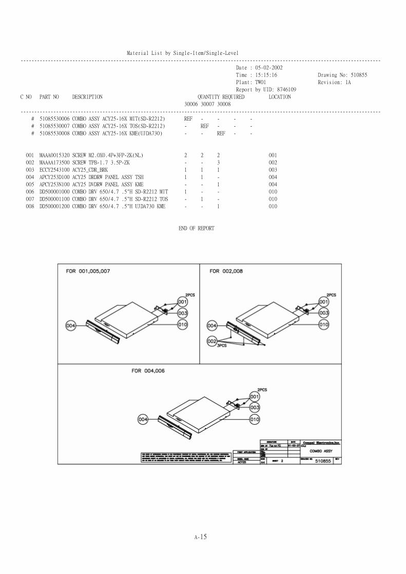
Material List by Single-Item/Single-Level
------------------------------------------------------------------------------------------------------------------------------------
Date : 05-02-2002
Time : 15:15:16 Drawing No: 510855
Plant: TW01 Revision: 1A
Report by UID: 8746109
C NO PART NO DESCRIPTION QUANTITY REQUIRED LOCATION
30006 30007 30008
------------------------------------------------------------------------------------------------------------------------------------
# 51085530006 COMBO ASSY ACY25-16X MIT(SD-R2212) REF - - - -
# 51085530007 COMBO ASSY ACY25-16X TOS(SD-R2212) - REF - - -
# 51085530008 COMBO ASSY ACY25-16X KME(UJDA730) - - REF - -
001 MAAA0015320 SCREW M2.0X0.4P+3FP-ZK(NL) 2 2 2 001
002 MAAAA173500 SCREW TPB-1.7 3.5P-ZK - - 3 002
003 ECCY2543100 ACY25_CDR_BRK 1 1 1 003
004 APCY253D100 ACY25 DRDRW PANEL ASSY TSH 1 1 - 004
005 APCY253N100 ACY25 DVDRW PANEL ASSY KME - - 1 004
006 DD500001000 COMBO DRV 650/4.7 .5"H SD-R2212 MIT 1 - - 010
007 DD500001100 COMBO DRV 650/4.7 .5"H SD-R2212 TOS - 1 - 010
008 DD500001200 COMBO DRV 650/4.7 .5"H UJDA730 KME - - 1 010
END OF REPORT
A-15
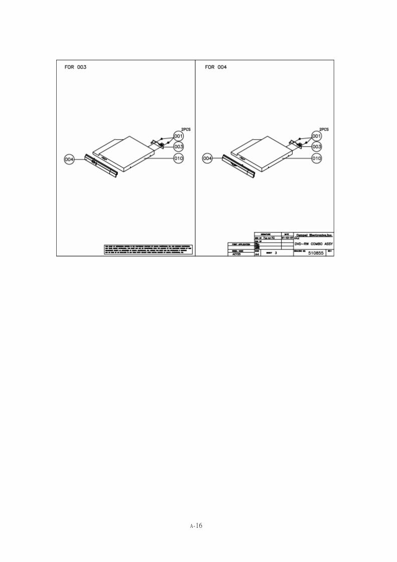
A-16
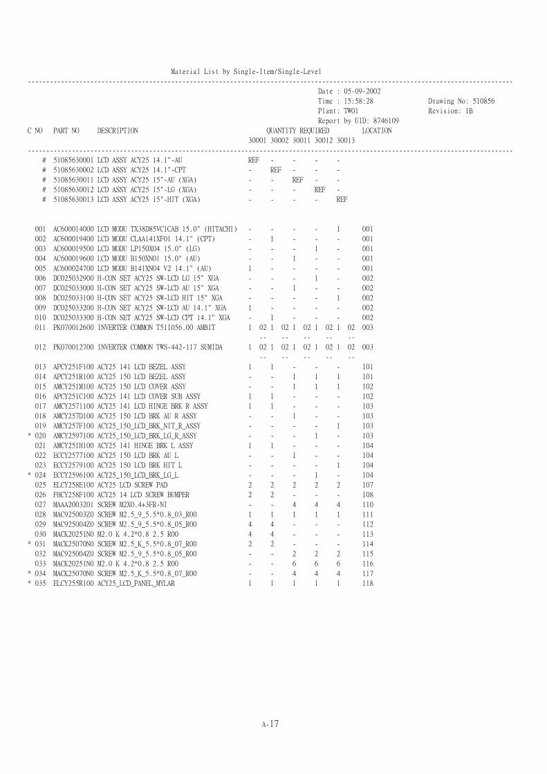
Material List by Single-Item/Single-Level
------------------------------------------------------------------------------------------------------------------------------------
Date : 05-09-2002
Time : 15:58:28 Drawing No: 510856
Plant: TW01 Revision: 1B
Report by UID: 8746109
C NO PART NO DESCRIPTION QUANTITY REQUIRED LOCATION
30001 30002 30011 30012 30013
------------------------------------------------------------------------------------------------------------------------------------
# 51085630001 LCD ASSY ACY25 14.1"-AU REF - - - -
# 51085630002 LCD ASSY ACY25 14.1"-CPT - REF - - -
# 51085630011 LCD ASSY ACY25 15"-AU (XGA) - - REF - -
# 51085630012 LCD ASSY ACY25 15"-LG (XGA) - - - REF -
# 51085630013 LCD ASSY ACY25 15"-HIT (XGA) - - - - REF
001 AC600014000 LCD MODU TX38D85VC1CAB 15.0" (HITACHI) - - - - 1 001
002 AC600019400 LCD MODU CLAA141XF01 14.1" (CPT) - 1 - - - 001
003 AC600019500 LCD MODU LP150X04 15.0" (LG) - - - 1 - 001
004 AC600019600 LCD MODU B150XN01 15.0" (AU) - - 1 - - 001
005 AC600024700 LCD MODU B141XN04 V2 14.1" (AU) 1 - - - - 001
006 DC025032900 H-CON SET ACY25 SW-LCD LG 15" XGA - - - 1 - 002
007 DC025033000 H-CON SET ACY25 SW-LCD AU 15" XGA - - 1 - - 002
008 DC025033100 H-CON SET ACY25 SW-LCD HIT 15" XGA - - - - 1 002
009 DC025033200 H-CON SET ACY25 SW-LCD AU 14.1" XGA 1 - - - - 002
010 DC025033300 H-CON SET ACY25 SW-LCD CPT 14.1" XGA - 1 - - - 002
011 PK070012600 INVERTER COMMON T51I056.00 AMBIT 1 02 1 02 1 02 1 02 1 02 003
-- -- -- -- --
012 PK070012700 INVERTER COMMON TWS-442-117 SUMIDA 1 02 1 02 1 02 1 02 1 02 003
-- -- -- -- --
013 APCY251F100 ACY25 141 LCD BEZEL ASSY 1 1 - - - 101
014 APCY251R100 ACY25 150 LCD BEZEL ASSY - - 1 1 1 101
015 AMCY251M100 ACY25 150 LCD COVER ASSY - - 1 1 1 102
016 APCY251C100 ACY25 141 LCD COVER SUB ASSY 1 1 - - - 102
017 AMCY2571100 ACY25 141 LCD HINGE BRK R ASSY 1 1 - - - 103
018 AMCY257D100 ACY25 150 LCD BRK AU R ASSY - - 1 - - 103
019 AMCY257F100 ACY25_150_LCD_BRK_NIT_R_ASSY - - - - 1 103
* 020 AMCY2597100 ACY25_150_LCD_BRK_LG_R_ASSY - - - 1 - 103
021 AMCY251H100 ACY25 141 HINGE BRK L ASSY 1 1 - - - 104
022 ECCY2577100 ACY25 150 LCD BRK AU L - - 1 - - 104
023 ECCY2579100 ACY25 150 LCD BRK HIT L - - - - 1 104
* 024 ECCY2596100 ACY25_150_LCD_BRK_LG_L - - - 1 - 104
025 ELCY258E100 ACY25 LCD SCREW PAD 2 2 2 2 2 107
026 FHCY258F100 ACY25 14 LCD SCREW BUMPER 2 2 - - - 108
027 MAAA2003201 SCREW M2X0.4+3FR-NI - - 4 4 4 110
028 MAC925003Z0 SCREW M2.5_9_5.5*0.8_03_R00 1 1 1 1 1 111
029 MAC925004Z0 SCREW M2.5_9_5.5*0.8_05_R00 4 4 - - - 112
030 MACK20251N0 M2.0 K 4.2*0.8 2.5 R00 4 4 - - - 113
* 031 MACK25070N0 SCREW M2.5_K_5.5*0.8_07_R00 2 2 - - - 114
032 MAC925004Z0 SCREW M2.5_9_5.5*0.8_05_R00 - - 2 2 2 115
033 MACK20251N0 M2.0 K 4.2*0.8 2.5 R00 - - 6 6 6 116
* 034 MACK25070N0 SCREW M2.5_K_5.5*0.8_07_R00 - - 4 4 4 117
* 035 ELCY255R100 ACY25_LCD_PANEL_MYLAR 1 1 1 1 1 118
A-17
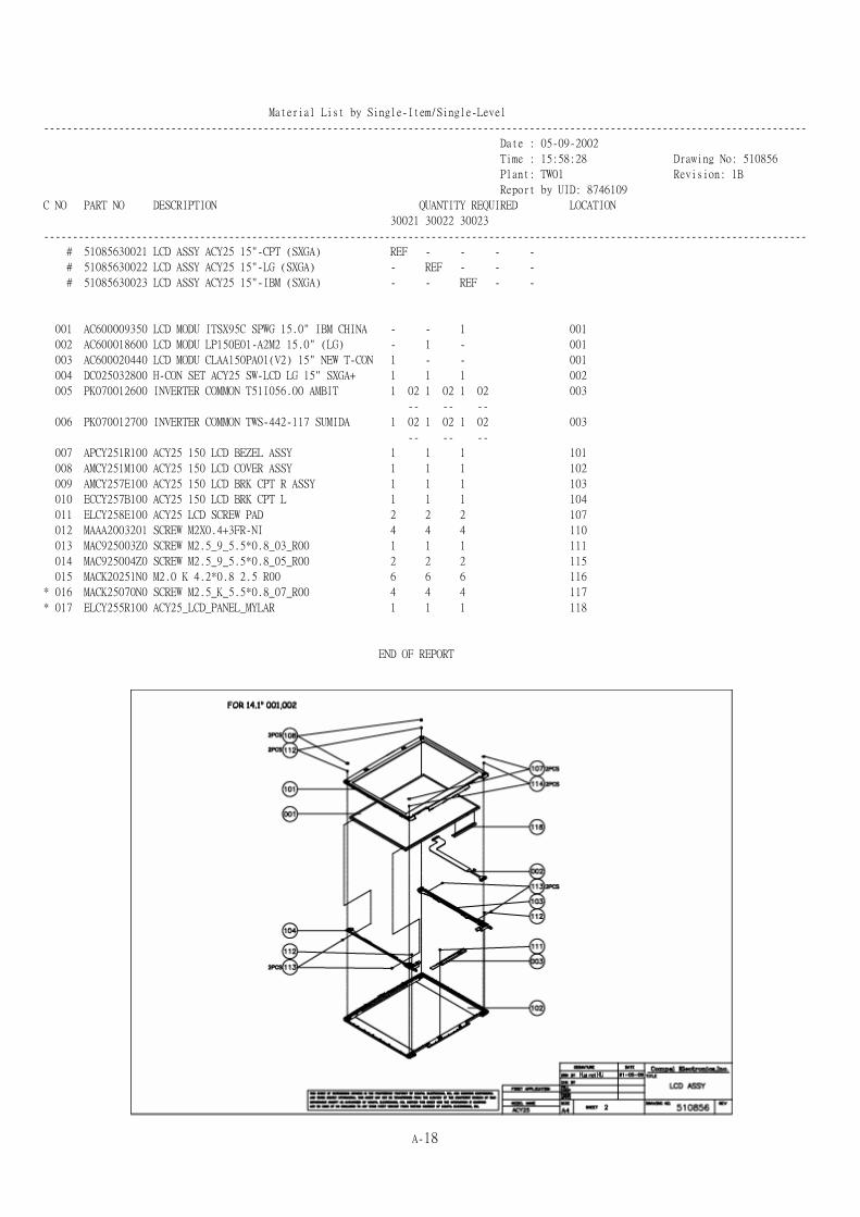
Material List by Single-Item/Single-Level
------------------------------------------------------------------------------------------------------------------------------------
Date : 05-09-2002
Time : 15:58:28 Drawing No: 510856
Plant: TW01 Revision: 1B
Report by UID: 8746109
C NO PART NO DESCRIPTION QUANTITY REQUIRED LOCATION
30021 30022 30023
------------------------------------------------------------------------------------------------------------------------------------
# 51085630021 LCD ASSY ACY25 15"-CPT (SXGA) REF - - - -
# 51085630022 LCD ASSY ACY25 15"-LG (SXGA) - REF - - -
# 51085630023 LCD ASSY ACY25 15"-IBM (SXGA) - - REF - -
001 AC600009350 LCD MODU ITSX95C SPWG 15.0" IBM CHINA - - 1 001
002 AC600018600 LCD MODU LP150E01-A2M2 15.0" (LG) - 1 - 001
003 AC600020440 LCD MODU CLAA150PA01(V2) 15" NEW T-CON 1 - - 001
004 DC025032800 H-CON SET ACY25 SW-LCD LG 15" SXGA+ 1 1 1 002
005 PK070012600 INVERTER COMMON T51I056.00 AMBIT 1 02 1 02 1 02 003
-- -- --
006 PK070012700 INVERTER COMMON TWS-442-117 SUMIDA 1 02 1 02 1 02 003
-- -- --
007 APCY251R100 ACY25 150 LCD BEZEL ASSY 1 1 1 101
008 AMCY251M100 ACY25 150 LCD COVER ASSY 1 1 1 102
009 AMCY257E100 ACY25 150 LCD BRK CPT R ASSY 1 1 1 103
010 ECCY257B100 ACY25 150 LCD BRK CPT L 1 1 1 104
011 ELCY258E100 ACY25 LCD SCREW PAD 2 2 2 107
012 MAAA2003201 SCREW M2X0.4+3FR-NI 4 4 4 110
013 MAC925003Z0 SCREW M2.5_9_5.5*0.8_03_R00 1 1 1 111
014 MAC925004Z0 SCREW M2.5_9_5.5*0.8_05_R00 2 2 2 115
015 MACK20251N0 M2.0 K 4.2*0.8 2.5 R00 6 6 6 116
* 016 MACK25070N0 SCREW M2.5_K_5.5*0.8_07_R00 4 4 4 117
* 017 ELCY255R100 ACY25_LCD_PANEL_MYLAR 1 1 1 118
END OF REPORT
A-18
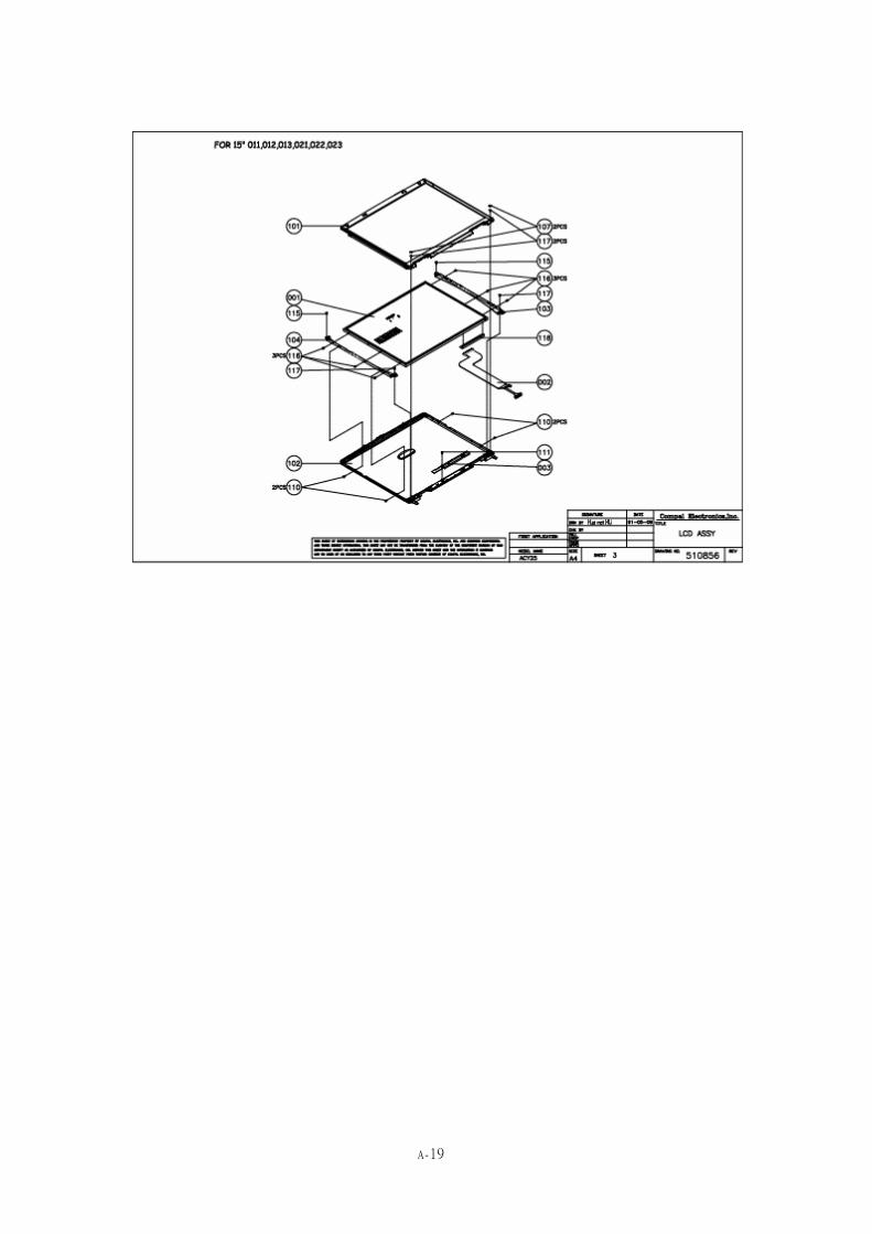
A-19
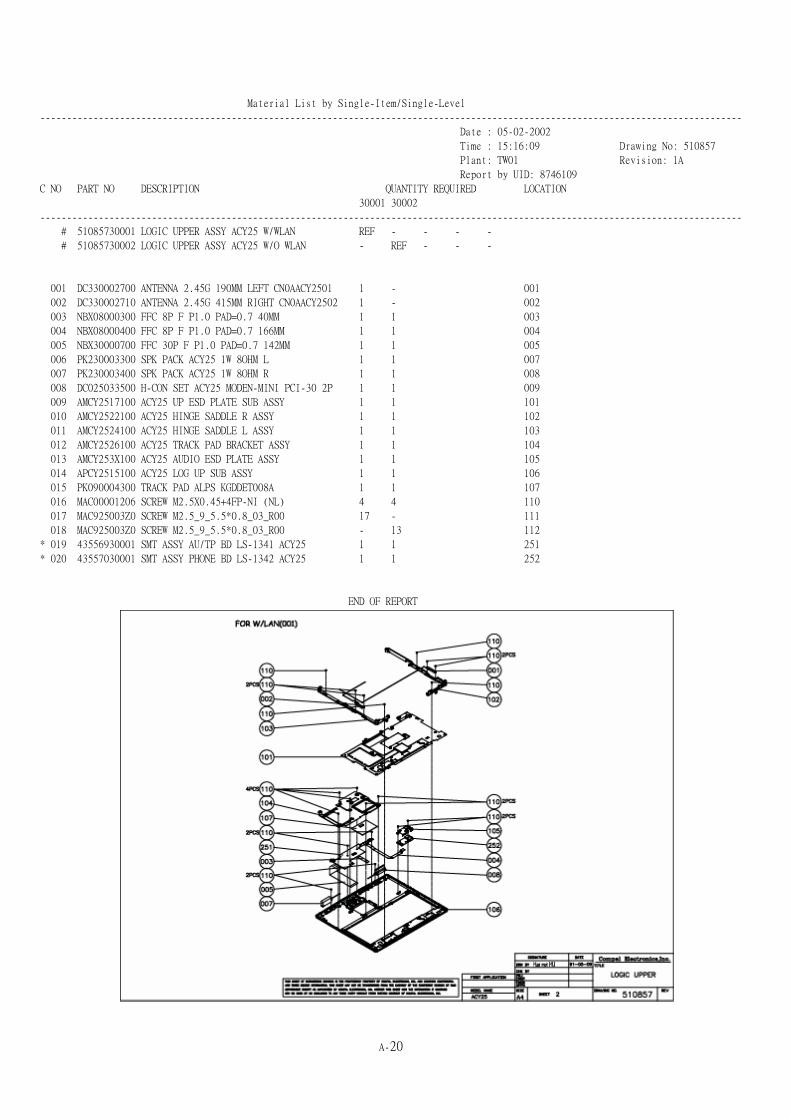
Material List by Single-Item/Single-Level
------------------------------------------------------------------------------------------------------------------------------------
Date : 05-02-2002
Time : 15:16:09 Drawing No: 510857
Plant: TW01 Revision: 1A
Report by UID: 8746109
C NO PART NO DESCRIPTION QUANTITY REQUIRED LOCATION
30001 30002
------------------------------------------------------------------------------------------------------------------------------------
# 51085730001 LOGIC UPPER ASSY ACY25 W/WLAN REF - - - -
# 51085730002 LOGIC UPPER ASSY ACY25 W/O WLAN - REF - - -
001 DC330002700 ANTENNA 2.45G 190MM LEFT CN0AACY2501 1 - 001
002 DC330002710 ANTENNA 2.45G 415MM RIGHT CN0AACY2502 1 - 002
003 NBX08000300 FFC 8P F P1.0 PAD=0.7 40MM 1 1 003
004 NBX08000400 FFC 8P F P1.0 PAD=0.7 166MM 1 1 004
005 NBX30000700 FFC 30P F P1.0 PAD=0.7 142MM 1 1 005
006 PK230003300 SPK PACK ACY25 1W 8OHM L 1 1 007
007 PK230003400 SPK PACK ACY25 1W 8OHM R 1 1 008
008 DC025033500 H-CON SET ACY25 MODEN-MINI PCI-30 2P 1 1 009
009 AMCY2517100 ACY25 UP ESD PLATE SUB ASSY 1 1 101
010 AMCY2522100 ACY25 HINGE SADDLE R ASSY 1 1 102
011 AMCY2524100 ACY25 HINGE SADDLE L ASSY 1 1 103
012 AMCY2526100 ACY25 TRACK PAD BRACKET ASSY 1 1 104
013 AMCY253X100 ACY25 AUDIO ESD PLATE ASSY 1 1 105
014 APCY2515100 ACY25 LOG UP SUB ASSY 1 1 106
015 PK090004300 TRACK PAD ALPS KGDDET008A 1 1 107
016 MAC00001206 SCREW M2.5X0.45+4FP-NI (NL) 4 4 110
017 MAC925003Z0 SCREW M2.5_9_5.5*0.8_03_R00 17 - 111
018 MAC925003Z0 SCREW M2.5_9_5.5*0.8_03_R00 - 13 112
* 019 43556930001 SMT ASSY AU/TP BD LS-1341 ACY25 1 1 251
* 020 43557030001 SMT ASSY PHONE BD LS-1342 ACY25 1 1 252
END OF REPORT
A-20
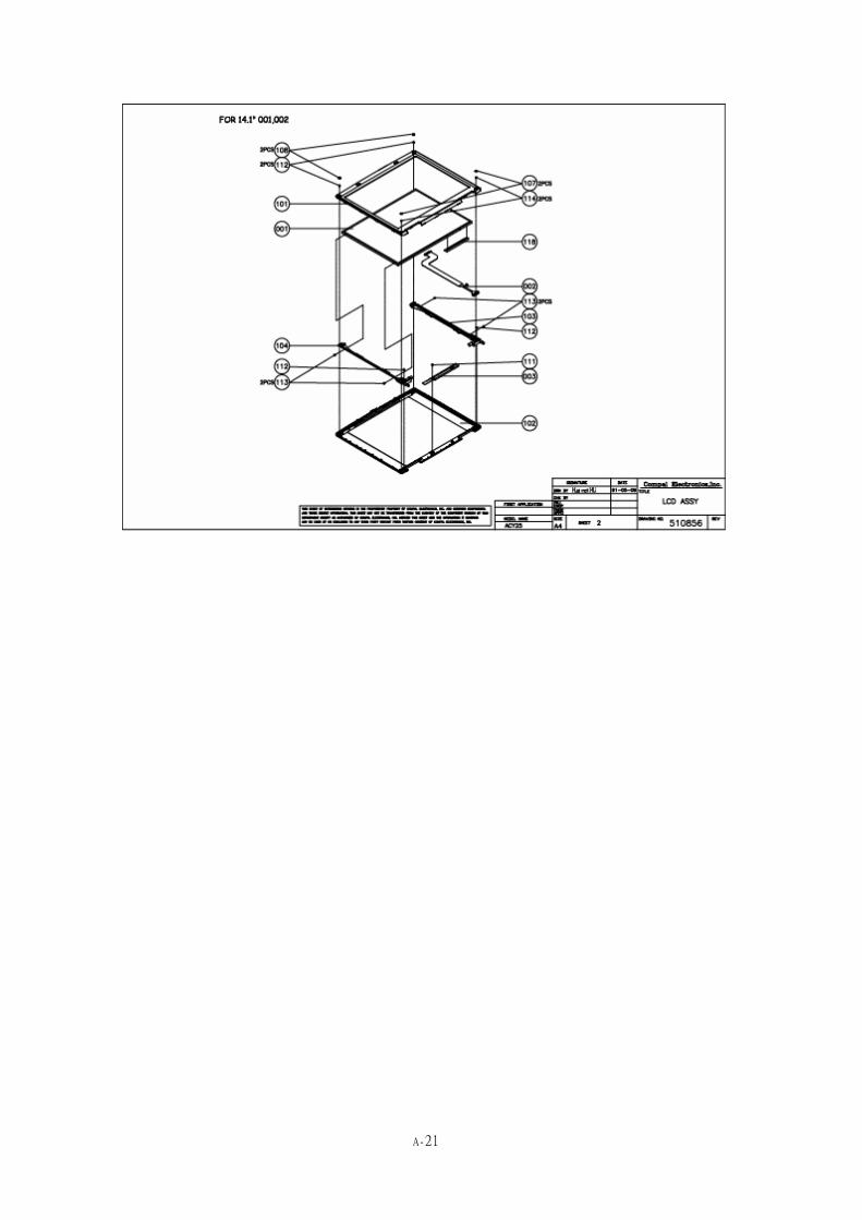
A-21
Material List by Single-Item/Single-Level
------------------------------------------------------------------------------------------------------------------------------------
Date : 05-02-2002
Time : 16:39:07 Drawing No: 54B601
Plant: TW01 Revision: 1A
Report by UID: 8746109
C NO PART NO DESCRIPTION QUANTITY REQUIRED LOCATION
30001 30002
------------------------------------------------------------------------------------------------------------------------------------
# 54B60130001 SYS UNIT ACY25-030 W/WLAN REF - - - -
# 54B60130002 SYS UNIT ACY25-030 W/O WLAN - REF - - -
001 PK010005700 F/D MODEM ACT10 1456VQL9Q(INT) - 1 007
002 PK293000200 W/M CARD ACT10 WLL030M ASKEY 1 - 008
003 46121030001 CPCBA,M/B LA-1341 ACY25 1 1 251
004 45557130001 PCBA SW BD LS-1343 ACY25 1 1 252
005 51085730001 LOGIC UPPER ASSY ACY25 W/WLAN 1 - 253
006 51085730002 LOGIC UPPER ASSY ACY25 W/O WLAN - 1 253
007 X6621330001 MEC PARTS ACY25 1 1 300
END OF REPORT
A-22
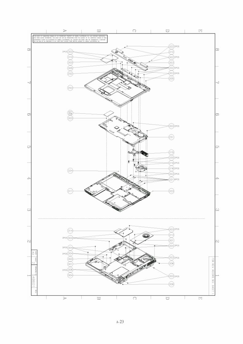
A-23
Table of contents:
1. System Description ------------------------------------------------------------------------ 1-1
Scope ------------------------------------------------------------------------------------------- 1-2
Electric Specifications -------------------------------------------------------------------- 1-4
2. Software Specification for System BIOS ------------------------------------------- 2-1
System Component Summary ---------------------------------------------------------- 2-1
Setup screens -------------------------------------------------------------------------------- 2-14
3. Hardware -------------------------------------------------------------------------------------- 3-1
Major Sub-assembly Specification ---------------------------------------------------- 3-1
4. Power Supply -------------------------------------------------------------------------------- 4-1
DC-DC Converter ---------------------------------------------------------------------------- 4-3
DC-DC Output -------------------------------------------------------------------------------- 4-4
ACY23 14.1,15” Inverter Specification ----------------------------------------------- 4-7
5. Disassembly ---------------------------------------------------------------------------------- 5-1
General ----------------------------------------------------------------------------------------- 5-1
Remove Battery Module ------------------------------------------------------------------ 5-7
Remove PC Card Module ----------------------------------------------------------------- 5-8
Remove Display Assembly -------------------------------------------------------------- 5-9
Remove Keyboard / button board ----------------------------------------------------- 5-17
Remove Wireless LAN / Modem Unit ------------------------------------------------- 5-19
Remove Expansion Memory ------------------------------------------------------------ 5-22
Remove CD-RW/DVD-ROM or CD-ROM/Combo Drive--------------------------- 5-25
Remove FDD Drive ------------------------------------------------------------------------- 5-27
Remove HDD Drive ------------------------------------------------------------------------ 5-29
Remove FAN ---------------------------------------------------------------------------------- 5-30
1Table contents
Chapter 1 2
Remove CPU --------------------------------------------------------------------------------- 5-31
Remove Top Cover ------------------------------------------------------------------------- 5-33
Remove Touch Pad ------------------------------------------------------------------------- 5-35
Remove Speakers --------------------------------------------------------------------------- 5-37
Remove Microphone jack ---------------------------------------------------------------- 5-38
Remove System board -------------------------------------------------------------------- 5-39 6. Testing and Troubleshooting ----------------------------------------------------------- 6-1
A. Spare Parts ----------------------------------------------------------------------------------- A-1