Embed Size (px)
Citation preview

Contents IndexPagePageChapterChapter
Chapter 1: Measurement and Extraction of BSIM4 Model ParametersThe following section summarizes some aspects of UCB�s BSIM4 Model and Agilent�s IC-CAP Modeling Package to measure and extract BSIM4 model parameters.
Basic effects modeled in BSIM4:� Short and narrow channel effects on threshold voltage
� Non-uniform doping effects
� Mobility reduction due to vertical field
� Bulk charge effect
� Carrier velocity saturation
� Drain induced barrier lowering (DIBL)
� Channel length modulation (CLM)
� Substrate current induced body effect (SCBE)
� Parasitic resistance effects
� Quantum mechanic charge thickness model
Enhanced drain current model� VTH model for pocket/retrograde technologies
� New predictive mobility model
� Gate induced drain leakage (GIDL)
� Internal/external bias-dependent drain source resistance
RF and high-speed model� Intrinsic input resistance (Rgate) model
� Non-Quasi-Static (NQS) model
� Holistic and noise-partition thermal noise model
� Substrate resistance network
6-1

Contents IndexPagePageChapterChapter
� Calculation of layout-dependent parasitic elements
� Asymmetrical source/drain junction diode model
� I-V and breakdown model
� Gate dielectric tunneling current model
Key features of the BSIM4 Modeling Package� The new graphical user interface in Agilent�s IC-CAP enables the quick setup of tests and
measurements followed by automatic parameter extraction routines.
� A new data management concept allows a powerful and flexible handling of measurement data using an open and easy data base concept.
� The powerful extraction procedures can be easily adopted to different CMOS processes. They support all possible configurations of the BSIM4 model.
� Quality assurance procedures are checking every step in the modeling flow from measurements to the final export of the SPICE model parameter set.
� The fully automatically generation of HTML reports is included to enable web publishing of a modeling project.
� The modeling package will support SPICE3e2 and major commercial simulator formats such as HSPICE, Spectre or Agilent�s ADS
The Modeling Package supports measurements on � DC transistors
� Parasitic diodes
� Capacitances
� Oxide
� Overlap
� Bulk-drain, source-drain junction
� Intrinsic
Extractions for � DC transistors
6-2

Contents IndexPagePageChapterChapter
� Parasitic diodes
� Capacitances
Data Structure inside the BSIM4 Modeling Package
6-3

Contents IndexPagePageChapterChapter
Measurement of MOSFET�s for the BSIM4 ModelThis part of the manual provides some background information to make necessary measurements of your devices. It will provide information on features of the BSIM4 Modeling Package, how to use the graphic user interface (GUI) and give you some hints on how to measure and what to measure using the right devices.
The GUI window is opened by double clicking on the BSIM4-Icon in the ICCAP main window. See Figure 1-1 for a screen shot of this window.
Figure 1-1. Starting the BSIM4 GUI from IC-CAP main window
6-4

Contents IndexPagePageChapterChapter
After you have double clicked the icon, the GUI window of the BSIM4 Modeling Package (Figure 1-2) comes up on your screen.
Figure 1-2. Part of Graphic User Interface of the BSIM4 Modeling Package.
The top row of the GUI shows a group of buttons on the left side to create a New project or to Open an already existing one, to Save or to Delete projects. You will be prompted before the selected action takes place.
The project name appears in the middle of the top row. It is shown on blue background, in Figure 1-2 the project is called �Example�.
On the right side of the GUI�s top row, you will find a Print button, which opens a dialog box.
Enter the command line for your specific printing device and press OK. The form will be printed.
The next button in the top row - Help - opens up the online manual - the file you are viewing right now.
In contrast to the function of this button, you�ll find a Help button on each folders lower left corner, too, which will open a short help document describing the task to be performed using this page. It will only give you information on how to use the buttons and forms associated with this task. Inside this manual, there are some in depth hints for the task, i.e which device geometries to use or how to connect the instrument to the device under test to get the best extraction results from your measurements.
The Info button, which is located to the right of the help button, gives you some information about the creators of the BSIM4 Modeling Package.
The fourth button in this group is the Demo button. Use this button to explore the BSIM4 modeling package features without starting actual measurements. This means, all measurement device drivers are disabled. Therefore, no measurement is possible in demo mode! This is also a convenient way to create a project without the need of a measurement license!
6-5

Contents IndexPagePageChapterChapter
Far to the right of the top row there is a button to Exit the BSIM4 modeling package.
Below the top row of buttons you will find a row of seven folders. Basically, each folder is assigned to a specific task in the measurement process. They are intended to be parsed from left to right, but you are not bound to that order.
The following paragraphs are assigned to one folder of the GUI each.
Project NotesThe notes folder is provided to store notes you take on a specific project, Figure 1-3 shows the notes form. You can enter general data like technology used to produce this wafer as well as lot, wafer and chip number. There is a field to enter the operator�s name and the date, the measurement has been taken. Space has been provided to enter notes on that project.
The notes you have entered, are saved under the project name in the middle of the top row using the Save button to the left of this form. In our example this project is called �Example�.
Figure 1-3. Notes folder of the BSIM4 Modeling Package�s GUI
6-6

Contents IndexPagePageChapterChapter
Measurement ConditionsThe next step in the modeling process is to set up measurement conditions for different measurement tasks like DC, CV or diode measurements.
This folder is designed for easy setup of conditions for DC Transistor and Capacitance as well as DC Diode measurements. Figure 1-4 shows the left part of the form.
Figure 1-4. Measurement Conditions Form
On the left side of the form, you will find a button to Save your setup under the name of the project in the middle of the top row - in our screen shot the name is �Example�.
6-7

Contents IndexPagePageChapterChapter
The measurement conditions form is divided into sections to enter the polarity of the devices to be measured and to define the conditions of DC Transistor, Capacitance and DC Diode measurements. See the chapters on DC Tansistor DUTs, Capacitance DUTs and DC Diode DUTs, respectively, for some background information on connecting the source-measurement units (SMU�s) and the CV instrument to the devices to be measured.
Polarity:There is a polarity switch where you can specify whether you are measuring NMOS or PMOS devices by pressing the appropriate button. Shown here is the measurement of NMOS devices.
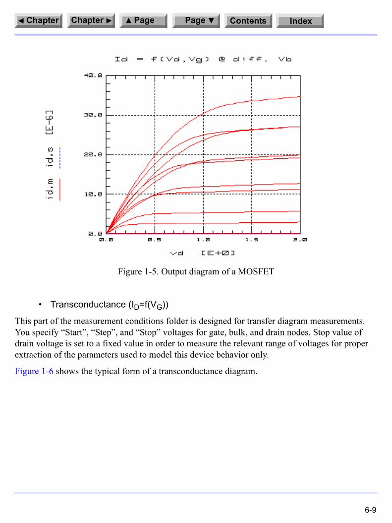
DC Transistor:� Output (ID=f(VD))
Here you specify the stimulus voltages used for measuring the output characteristic of your devices. You define �Start�, �Step�, and �Stop� voltages for drain, gate, and bulk nodes, respectively. For some of the values to be specified you will find a gray shaded entry field. This means, no data can be entered into this field to prevent conditions which could lead to inconsistent parameter extraction. Figure 1-5 shows a typically measured output characteristic of a MOSFET.
6-8
Contents IndexPagePageChapterChapter
Figure 1-5. Output diagram of a MOSFET
� Transconductance (ID=f(VG))
This part of the measurement conditions folder is designed for transfer diagram measurements. You specify �Start�, �Step�, and �Stop� voltages for gate, bulk, and drain nodes. Stop value of drain voltage is set to a fixed value in order to measure the relevant range of voltages for proper extraction of the parameters used to model this device behavior only.
Figure 1-6 shows the typical form of a transconductance diagram.
6-9
Contents IndexPagePageChapterChapter
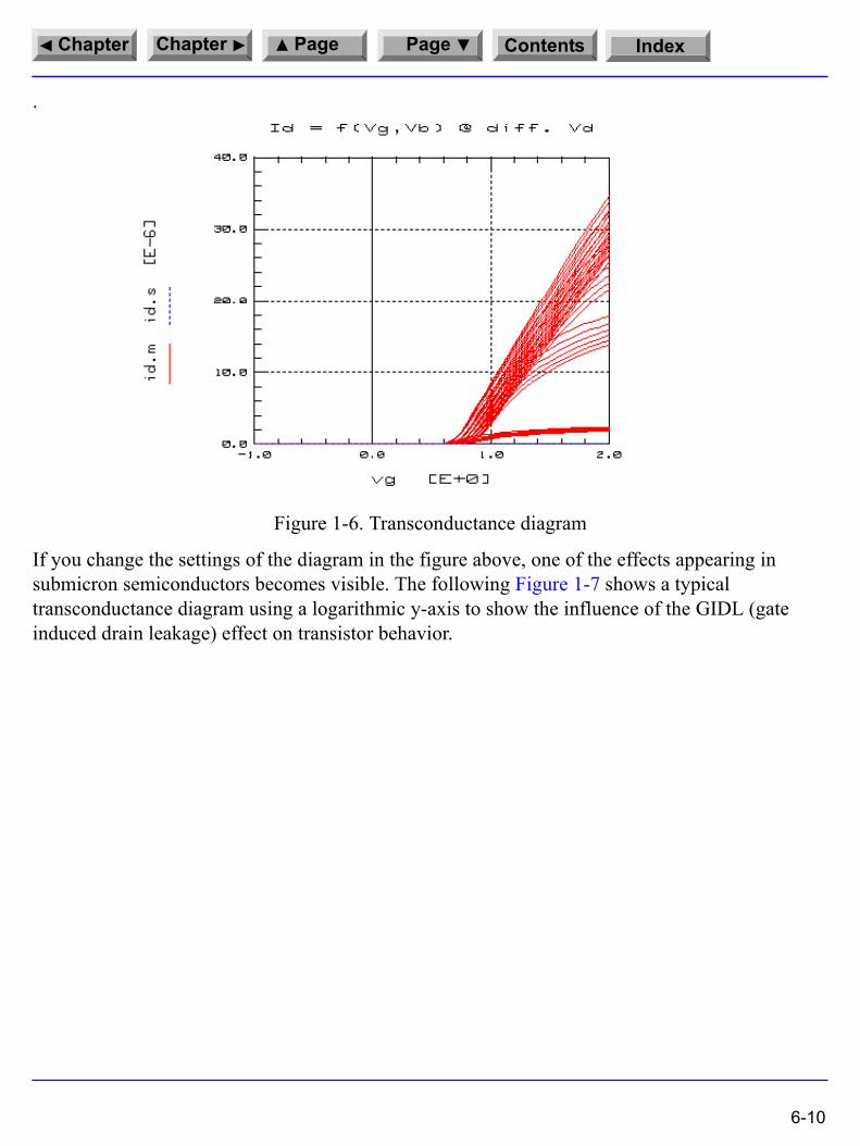
.
Figure 1-6. Transconductance diagram
If you change the settings of the diagram in the figure above, one of the effects appearing in submicron semiconductors becomes visible. The following Figure 1-7 shows a typical transconductance diagram using a logarithmic y-axis to show the influence of the GIDL (gate induced drain leakage) effect on transistor behavior.
6-10

Contents IndexPagePageChapterChapter
Figure 1-7. Transconductance diagram showing GIDL effect
6-11

Contents IndexPagePageChapterChapter
The following figure shows the right part of the measurement conditions folder.
Figure 1-8. Right part of measurement conditions folder
Capacitance:This section is used to define capacitance measurement conditions for junction, oxide/overlap and intrinsic capacities. See Figure 1-9 for a definition of capacitances on a MOSFET.
6-12

Contents IndexPagePageChapterChapter
Figure 1-9. Definition of capacitances on a MOSFET
� Junction
Enter the �Start�, �Step�, and �Stop� values for the bulk voltage used to measure junction capacitance of drain/bulk and source/bulk junctions.
� Oxide/Overlap
Please give values for �Step� and �Stop� voltage used in measuring gate/source, gate/drain and gate/bulk overlap capacities as well as oxide fringing capacity. Start value of the gate voltage is set to a value usually save for the devices to be measured.
� Intrinsic
Here you can specify values for drain and gate voltages used to measure intrinsic capacitances.
DC DiodeThis part of the measurement conditions folder is used to define DC measurements on source/drain-bulk diodes. To be defined is the �Start�, �Step�, and �Stop� voltage for the SMU connected to the drain node. Figure 1-10 shows a cross section of a MOSFET with the source-bulk diode.
Region ofintrinsic capacity
CGDOL
CF
CGDO
Cjunc
6-13

Contents IndexPagePageChapterChapter
Figure 1-10. Measurement of source/drain-bulk diodes
Temperature SetupThis form is intended to define measurements at specified temperatures. Basically, the measurement of all DUT�s is to be performed at SPICE default temperature TNOM, which should be between 20° and 27° Celsius. This temperature could not be deleted.
p +
n +
6-14

Contents IndexPagePageChapterChapter
Note: Please don�t forget to enter the actual temperature during measurement of the devices. Figure 1-11 shows the Temperature Setup folder.
Figure 1-11. Temperature Setup form
Using the buttons provided on the left side of the form, you can Add new temperatures. Enter the desired temperature into the dialog box. Please be sure to enter the appropriate value in degrees Celsius (°C).
If you would like to Delete a measurement temperature, you will be prompted for the temperature to be deleted. If there is a file containing measured data for this temperature, the data file will be deleted if you click OK on the prompt dialog form, see Figure 1-12 below.
Figure 1-12. Dialog boxes to delete temperatures and measured data files, where applicable
6-15

Contents IndexPagePageChapterChapter
Note: You cannot delete the nominal temperature TNOM!
Adding new measurement temperatures results in adding a new column for each of this temperatures in the three DUTs forms (DC Transistor, Capacitance and DC Diode).
Any changes on the Temperature Setup form must be saved prior to selecting another one.
6-16

Contents IndexPagePageChapterChapter
Switch MatrixWithin this form, which is shown in Figure 1-13, you select the kind of measurement you are using a switch matrix for. There are three options: Use switch matrix for DC Transistor Measurements, for Capacitance Measurements and for Diode Measurements. You can select any one or more than one by activating the predefined button(s).
Figure 1-13. Defining the use of a switch matrix for measurements
The Basic Settings provide choice of three different Matrix Models, which are supported by IC-CAP. Enter the appropriate Bus and HP-IB address of the Switch Matrix (22 in our example) as well as the HP-IB-Interface name. See the IC-CAP manual on �Making Measurements� for a
6-17

Contents IndexPagePageChapterChapter
complete description of the HP-IB settings of the switch matrix to be used. Our example shows the use of a 4085 matrix model. For this type of instrument you have to define which port is connected to what SMU or C meter input pin.
Again, you have to save your changes prior to leaving this form.
The actual pin connections are to be entered into the form selected for use of a switch matrix (one of the DC DUTs, Capacitance DUTs or Diode DUTs form or all of them). For example, if you have selected DC Transistor measurements for use with a switch matrix, you must enter the switch matrix pin numbers in the fields below the node names of the transistors to be measured on the DC Transistor DUTs form. This might be especially useful if you make series measurements on wafers using a probe card e.g. for quality control.
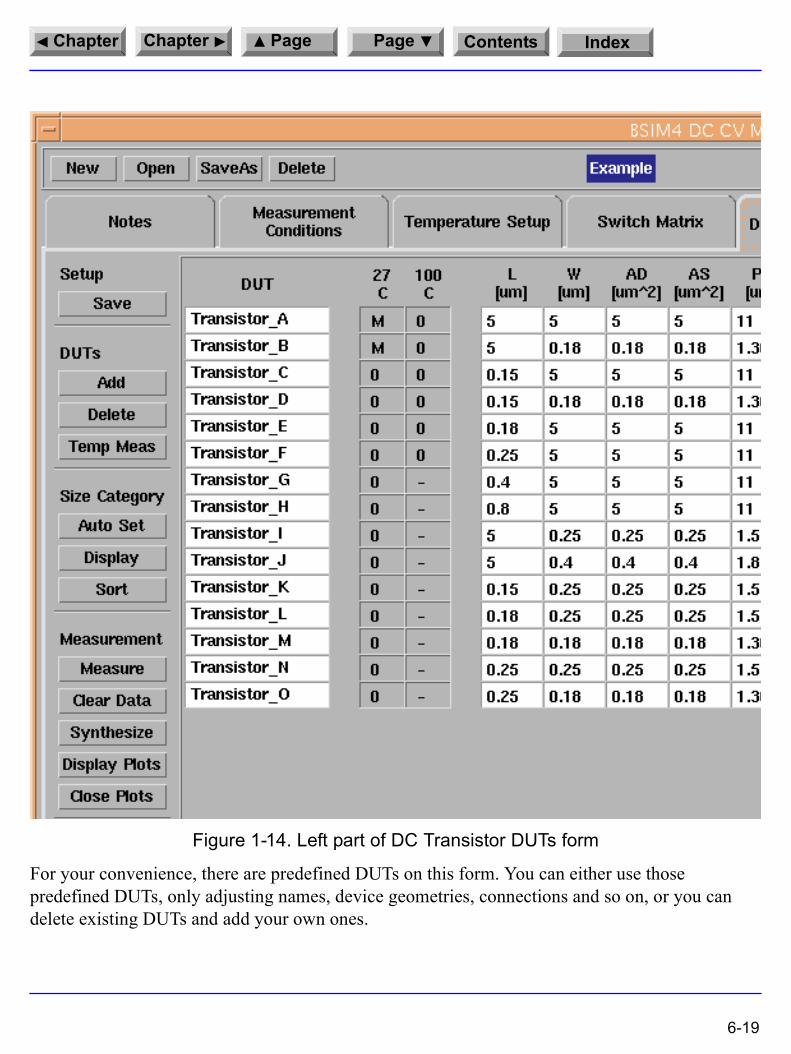
DC Tansistor DUTsThe DC Transistor DUTs form is used to enter DUT names, geometries and connections to the appropriate DUTs.
Figure 1-14 shows the right part of the DC Transistor DUTs form.
6-18
Contents IndexPagePageChapterChapter
Figure 1-14. Left part of DC Transistor DUTs form
For your convenience, there are predefined DUTs on this form. You can either use those predefined DUTs, only adjusting names, device geometries, connections and so on, or you can delete existing DUTs and add your own ones.
6-19
Contents IndexPagePageChapterChapter
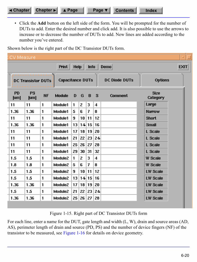
� Click the Add button on the left side of the form. You will be prompted for the number of DUTs to add. Enter the desired number and click add. It is also possible to use the arrows to increase or to decrease the number of DUTs to add. New lines are added according to the number you�ve entered.
Shown below is the right part of the DC Transistor DUTs form.
Figure 1-15. Right part of DC Transistor DUTs form
For each line, enter a name for the DUT, gate length and width (L, W), drain and source areas (AD, AS), perimeter length of drain and source (PD, PS) and the number of device fingers (NF) of the transistor to be measured, see Figure 1-16 for details on device geometry.
6-20

Contents IndexPagePageChapterChapter
If you have no knowledge of drain or source perimeter length, those data is approximated by BSIM4. For further details on how BSIM4 calculates perimeter data, see the BSIM4 manual from the University of California at Berkeley [1].
Remember, all geometries are to be given in microns (µm).
Geometries:
Shown here is a section of a MOSFET where you can find the geometries required by the BSIM4 modeling package.
Figure 1-16. .Cross section of a MOSFET showing device geometries
Figure 1-17. Top view of a multifinger MOSFET
p +
n +
L
DG
SDrain PerimeterPD
Drain AreaAD
WB
Bulk
Source
Gate
Drain
NF = 4
number of fingers:
G
DD SS S
6-21
Contents IndexPagePageChapterChapter
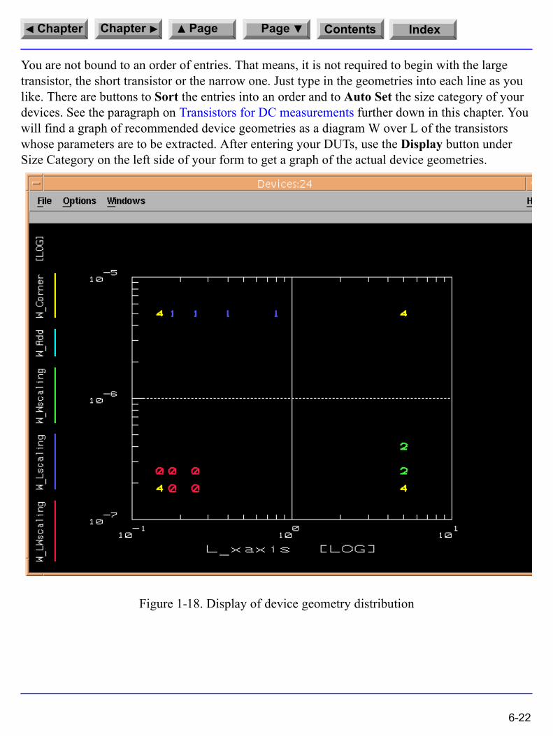
You are not bound to an order of entries. That means, it is not required to begin with the large transistor, the short transistor or the narrow one. Just type in the geometries into each line as you like. There are buttons to Sort the entries into an order and to Auto Set the size category of your devices. See the paragraph on Transistors for DC measurements further down in this chapter. You will find a graph of recommended device geometries as a diagram W over L of the transistors whose parameters are to be extracted. After entering your DUTs, use the Display button under Size Category on the left side of your form to get a graph of the actual device geometries.
Figure 1-18. Display of device geometry distribution
6-22

Contents IndexPagePageChapterChapter
You can compare your settings to the graph shown in Figure 1-18 to see, if your entries fulfil the requirements for proper parameter extraction. If the geometries entered fit into the rectangle of device geometries shown in the figure mentioned above, you can use the Auto Set button to set the Size Category of your devices automatically. Otherwise, you are required to enter size category manually using a form as shown in Figure 1-19 below.
Figure 1-19. Set size category
If you would like to delete DUTs:
� Click the Delete button on the left side of the form. You will be prompted with a list of DUTs (Figure 1-20). Select the DUTs to be deleted and click Delete on the Delete DUT form. A prompt dialog box appears. Select OK if you are satisfied with your choice of DUTs to be deleted.
Figure 1-20. Delete DUTs form
6-23
Contents IndexPagePageChapterChapter
According to your choice of temperatures on the Temperature Setup form, one or more columns marked with the temperatures you�ve entered appear. The fields of those columns show either (0) for no measured data available, (M) for DUT already measured or (-) for DUT not to be measured at that temperature.
� To select devices to be measured at different temperatures: Click the Temp Meas button on the left side of the form. You will be prompted with a list of DUTs. Select the devices to be measured at those temperatures entered in the Temperature Setup folder and click OK.
Note: You cannot exclude a DUT to be measured at TNOM. All DUTs are measured automatically at that temperature. If you have entered one or more temperatures on the Temperature Setup form, the DUTs selected for temperature measurement are all measured at those temperatures. It is not possible to select a DUT for measurement at temperature T1 but not at another temperature T2.
The minimum configuration to extract temperature effects on parameters includes a large, a short and a small device!
You can enter a module name and a comment for each DUT. If you are using a switch matrix, you must enter the pin numbers of the switch matrix pin connections to the transistor in the fields below the node names, see Figure 1-21 for details.
Note: When using module names to measure devices with probe cards, pay attention to the node numbers you are entering. Each device uses 4 connections to the switch matrix. You must enter the correct pin numbers for each DUT and not exceed the total pin count for each port of your matrix.
Connections to the DUTs:
6-24

Contents IndexPagePageChapterChapter
The following figure Figure 1-21 shows an example for a connected device under test (DUT) to the source measurement unit�s (SMU�s) during DC Transistor measurements.
Figure 1-21. SMU connections to the device under test
Measurement of the devicesOnce all DUTs are entered with their respective geometries, switch matrix pin connection and measurement temperatures, the actual measurement of devices can take place. You will find the appropriate buttons under the �Measurement� section on the left side of the DC Transistor DUTs folder.
DUTDB
S
G
SMU1 SMU2 SMU3 SMU4
Switch matrix Pin #,
see the short DUT, Transistor_C,in Fig. 1-14, 1_15
10 12 11 9
6-25

Contents IndexPagePageChapterChapter
� To start measurement of the devices: Click Measure and select the DUT(s) to be measured on the form (Figure 1-22) that opens. You can select measurement temperature (if there is a temperature other than TNOM defined in the temperature setup form) as well as a specific DUT or all DUTs in a module. Start measurement with the Measure button on that form. If measuring at elevated temperatures, be sure to wait until your devices are heated up or cooled down to the desired temperature. Please, be aware of the fact, that you must set your chuck temperature manually, because ICCAP does�nt support heated chuck drivers.
If you select measurement of all DUTs in a module, all DUTs are measured automatically if the use of a switch matrix activated.
Figure 1-22. Select devices and measurement temperatures form
� If you would like to clear some or all measured data, use the Clear button. You can select whether you would like to clear measured data of some or all DUT(s) at specified temperatures and click Clear Data to delete measured data files.
6-26

Contents IndexPagePageChapterChapter
� Using the Synthesize button, you are able to simulate data from existing model parameters. By selecting this feature, already measured data files are overwritten with synthesized data. You will be prompted (Figure 1-23) before existing data files are overwritten.
Figure 1-23. Prompt dialog for synthesizing measurement data
This synthesized data uses the voltages set on the Measurement Conditions form to generate �measurement� data from a known set of SPICE parameters. This might be especially useful to convert parameters of other models into BSIM4 parameters by loading the created �measurement data� into the extraction routines and extract BSIM4 parameters.
� For a glance at the diagrams that are just been measured, use the Display Plots button. You will see a form (Figure 1-24) to select which measured data set you would like to display. After choosing the plots, use the Display Plots button on that form to open up the plots desired. This is a convenient way to detect measurement errors before starting the extraction routines.
Figure 1-24. Selecting measured data to be displayed
6-27

Contents IndexPagePageChapterChapter
� If you are satisfied with data you have just measured, use the Close Plots button to close the plots of measured data.
Test structures for Deep Submicron CMOS ProcessesA very important prerequisite for a proper model parameter extraction is the selection of appropriate test structures. The following subsections describe the necessary test structures for proper determination of CV and DC model parameters. A very detailed description of ideal test structures can be found in the JESSI AC-41 reports [2].
Transistors for DC measurementsThe minimum set of devices for a proper extraction of DC model parameters is marked with ' ' in Figure 1-25. This means one transistor with large and wide channel (and therefore showing no short/narrow effects), one transistor with a narrow channel, one transistor with a short channel and one device with both, short and narrow channel. Please note that with this minimum set of devices some parameters cannot be determined correctly (see the chapter �Extraction of parameters�) and they are set to default values during the extraction. For an extraction of all model parameters and a better fit of the simulated devices over the whole range of designed gate length and gate width it is recommended to use more devices with different gate lengths and gate widths as shown in Figure 1-25 with ' ' signs. You can use additional devices e.g. for evaluating the extraction results for certain channel lengths and widths used in your process. They are marked � �.
6-28

Contents IndexPagePageChapterChapter
Figure 1-25. Recommended Test Transistor Geometries for proper parameter extraction
If you do not have test structures like the ones shown in Figure 1-25, you must be aware, extraction results may not be as accurate as in the ideal case shown above.
If your test structures consist of parallel transistors (e.g. 10 NARROW transistors in parallel), perform all the macros as usual. After the measurements are done, change the BSIM4 model parameter NF (number of device fingers) to 10 in our example. After that, you may continue using the extraction routines as usual.
Requirements for Devices Large
For a proper extraction of the basic model parameters, the short and narrow channel effects should not affect the large device extraction. Also the drain-source-resistance parameters should not have an influence on the simulated behavior of the large device. For a typical 0.25 micron CMOS process with a gate oxide thickness of 6 - 7nm a large device with channel length of 10 microns and channel width of 10 microns was found to meet these requirements.
Forbidden area due toprocess limitations
Design spacedirectly covered by extraction
Extended design space, extrapolated from extraction
6-29

Contents IndexPagePageChapterChapter
You can check this prerequisite if you only extract the parameters in the idvg/Large setup and then perform a simulation of the setup idvg/Large. After that simulation, perform the other geometry extractions and re-simulate the idvg/Large setup again. Now, the diagram ID = f(Vgs) should not change more than roughly 5% compared to the first simulation. If there is more difference, a larger device should be used to enable a good extraction of basic model parameters.
Narrow
For the category 'Narrow' you should use a device with the smallest designed gate width of your process. Using more narrow devices will increase the number of parameters which can be extracted and will lead to a better fit of the curves over the range of different channel widths.
ShortFor the category 'Short' you should use a device with the shortest designed gate length of your process. Using more short devices will increase the number of parameters which can be extracted and will lead to a better fit of the curves over the range of different channel lengths.
SmallFor the category 'Small' you should use a device with the shortest designed gate length and the smallest designed gate width of your process. This small device will incorporate all short and narrow channel effects and will be an indicator how good your parameter extractions are.
In generalIt is recommended to use the designed gate lengths and widths. Effects due to under diffusion or decrease of poly-Si gate length are sufficiently covered by the extraction routines and the model itself.
6-30

Contents IndexPagePageChapterChapter
Capacitance DUTsThis form is used to measure capacitances of devices and to display measured data.
Figure 1-26. Right part of the Capacitance DUTs form
6-31

Contents IndexPagePageChapterChapter
Figure 1-27. Left part of the Capacitance DUTs folder
Within this form, you will find fields to enter names of DUTs, geometries and switch matrix connections, and to select temperatures at which to measure the DUTs.
� To add new DUTs: Click the Add button on the left side of the form. You will be prompted for a group of capacitances to add DUTs to (Figure 1-28). Select the desired group (junction
6-32

Contents IndexPagePageChapterChapter
bulk-drain or bulk-source, oxide, overlap or intrinsic) and click add. New lines are added according to the selection you�ve made.
Note: Selecting overlap capacitances actually adds two DUTs: Overlap_GDS and Overlap_GDSB. It is required for proper parameter extraction to measure both DUTs and extract the parameters from both measurements. Therefore, it only makes sense to add those DUTs together.
Figure 1-28. Add DUTs to measure capacity
For each line, you can change the predefined name for the DUT and enter necessary geometrical data. For your convenience, only relevant data is to be entered for a specific group of capacities. Relevant data fields are shown with white background and can be edited, grey shaded data fields are not editable. For example, DUTs to measure bulk-drain junction capacitances do not require gate length and width (L, W), source area (AS) and perimeter length of source (PS) geometrical data. You only have to enter drain area (AD) and drain perimeter (PD) as well as the number of device fingers (NF) of the transistor to be measured. See Figure 1-29 for some details on capacitances and geometries.
6-33

Contents IndexPagePageChapterChapter
Remember, all geometries are to be given in microns (µm).
Figure 1-29. Device geometries
According to your choice of temperatures on the Temperature Setup form, one or more columns marked with the temperatures you�ve entered appear. The fields of those columns show either (0) for no measured data available, (M) for DUT already measured or (-) for DUT not to be measured at that temperature.
You can enter a module name and a comment for each DUT. When using module names, you are able to measure one complete module with all his DUTs at once. This is intended for use of a prober card and taking measurements using the �step and repeat� function of a wafer prober. If you are using a switch matrix, you must enter the pin numbers of the switch matrix pin connections to the capacity you�re about to measure. The fields for high and low connection of the CV measuring instrument is marked H or L respectively. See the paragraph on �Test Structures for CV Measurements� for details on device geometries and requirements for proper extraction of capacitances of your devices like test lead connections and so on.
PSSource Perimeter
6-34

Contents IndexPagePageChapterChapter
� To delete DUTs: Click the Delete button on the left side of the form. You will be prompted with a list of DUTs. Select the DUT(s) to be deleted and click Delete on the Delete DUT form. A prompt dialog box appears. Select OK if you are satisfied with your choice of DUTs to be deleted.
� To select devices to be measured at different temperatures: Click the Temp Meas button on the left side of the form. You will be prompted with a list of DUTs. Select the devices to be measured at those temperatures entered in the Temperature Setup form and click OK.
Note: You cannot exclude a DUT to be measured at TNOM. All DUTs are measured automatically at that temperature. If you have entered one or more temperatures on the Temperature Setup form, the DUTs selected for temperature measurement are all measured at those temperatures. It is not possible to select a DUT for measurement at temperature T1 but not at another temperature T2.
� To start measurement of the devices: Click Measure and select the DUT(s) to be measured on the form that opens. You can select measurement temperature (if there is a temperature other than TNOM defined in the temperature setup form) as well as a specific DUT or all DUTs. Start measurement with the Measure button on that form. If measuring at elevated temperatures, be sure to wait until your devices are heated up or cooled down to the desired temperature.
6-35

Contents IndexPagePageChapterChapter
Figure 1-30. Selecting DUTs to be measured
� If you would like to clear some or all measured data, use the Clear button. You can select whether you would like to clear measured data of some or all DUT(s) at specified temperatures and click Clear Data to delete measured data files.
6-36

Contents IndexPagePageChapterChapter
Figure 1-31. Selcting DUTs to be deleted
� Using the Synthesize button, you are able to simulate data from existing parameters. This synthesized data uses the voltages set on the Measurement Conditions form to generate �measurement� data from a known set of SPICE parameters. This might be especially useful
6-37

Contents IndexPagePageChapterChapter
to convert parameters of other models into BSIM4 parameters by loading the created �measurement data� into the extraction routines and extract BSIM4 parameters.
Figure 1-32. Synthesize Data Prompt
� For a glance at the diagrams that are just been measured, use the Display Plots button. You will get a form to select which measured data set you would like to display. After choosing the plots you would like to see, use the Display Plots button on that form to open up the plots desired. This is a convenient way to detect measurement errors before starting the extraction routines.
Figure 1-33. Choose the plots of measured data to be displayed
� If you are satisfied with data you have just measured, use the Close Plots button to close the windows which show diagrams of measured data.
6-38

Contents IndexPagePageChapterChapter
Physically connecting test structures to your Capacitance Measurement DeviceFigure 1-34 shows how to connect the CV instrument to measure oxide and overlap capacitances. See also the following paragraph on test structures for CV measurement. In Table 1-1 you�ll find recommended test structures for specific capacitances to be measured together with recommended instrument connections.
Figure 1-34. Measurement of oxide and overlap capacitance
The following Figure 1-35 shows a typical gate-to-drain/source overlap capacitance diagram you would expect to measure with such type of connection and the default values for �Start�, �Step�, and �Stop� voltage VG.
6-39

Contents IndexPagePageChapterChapter
Figure 1-35. Example diagram of measured overlap capacity
Test Structures for CV Measurements
Table 1-1. Test Structures for CV Measurements
Category Shape Applied bias (n-type) Comment
BD Area /BS Area(pn-junction)
Area diode with large area, small perimeter and the doping concentration n+ of the drain/source region (shown here for n-type devices).
min(C g_sdb )
6-40

Contents IndexPagePageChapterChapter
BD Perim/BS Perim(pn-junction)
Finger diode of large perimeter, small area and the doping concentration n+ of the drain/source region (shown here for n-type devices).
BD_Perim_ Gate/ BS_Perim_ Gate(pn-junction)
Finger diode with large perimeter and small area and the doping concentration n+ of the LDD region (shown here for n-type devices).
Oxide(Gate oxide)
Large area MOS capacitor
Overlap GDS(Overlap gate - drain/source)
A large number of parallel switched LDD MOS transistors (e.g. 200 transistors with L=0.25µm, W=10.0µm) or multi-finger transistors (see shape)
Table 1-1. Test Structures for CV Measurements
6-41
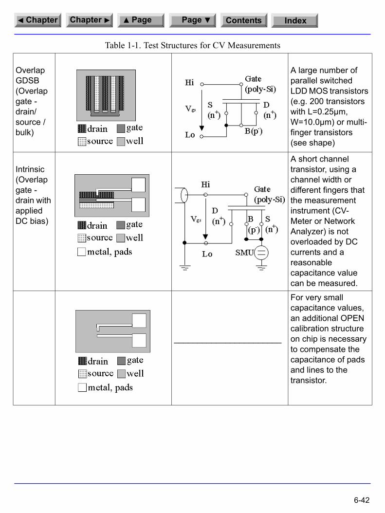
Contents IndexPagePageChapterChapter
Overlap GDSB(Overlap gate - drain/source /bulk)
A large number of parallel switched LDD MOS transistors (e.g. 200 transistors with L=0.25µm, W=10.0µm) or multi-finger transistors (see shape)
Intrinsic(Overlap gate - drain with applied DC bias)
A short channel transistor, using a channel width or different fingers that the measurement instrument (CV-Meter or Network Analyzer) is not overloaded by DC currents and a reasonable capacitance value can be measured.
_______________________
For very small capacitance values, an additional OPEN calibration structure on chip is necessary to compensate the capacitance of pads and lines to the transistor.
Table 1-1. Test Structures for CV Measurements
6-42
Contents IndexPagePageChapterChapter
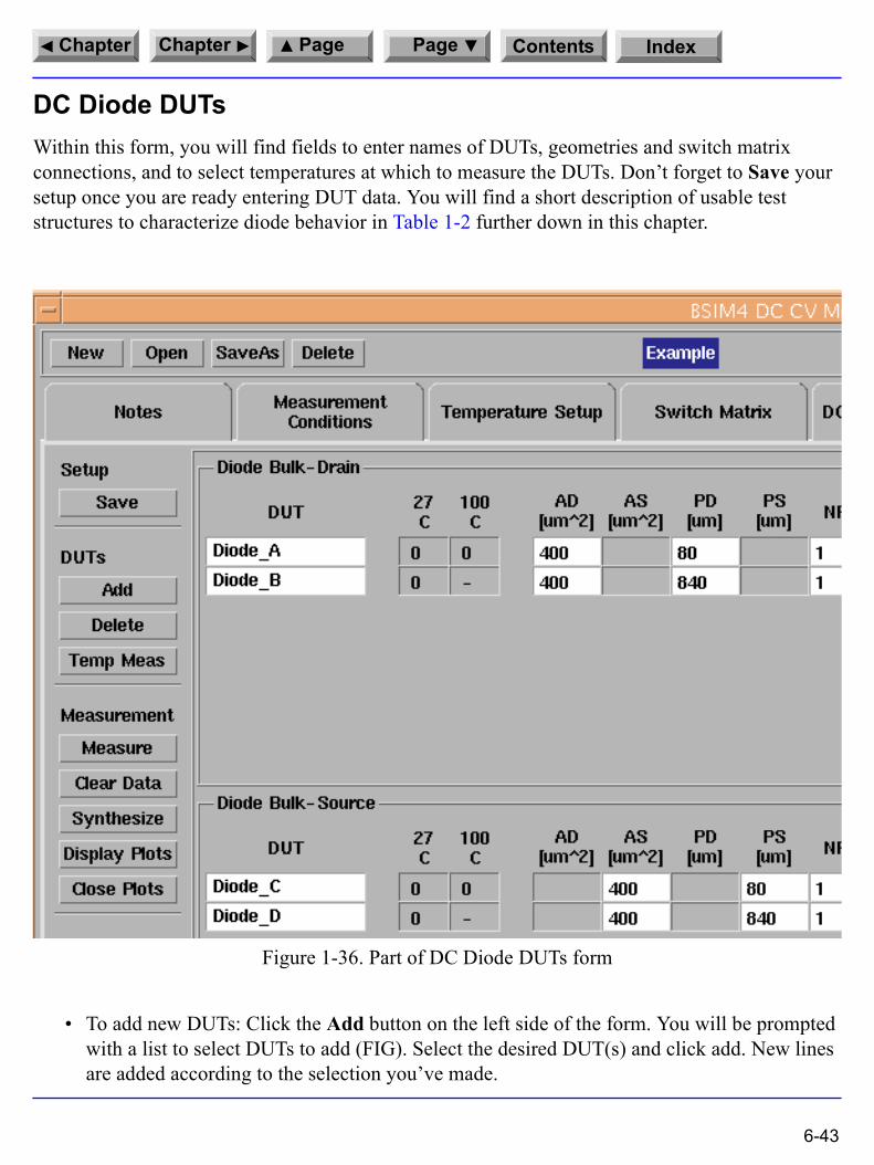
DC Diode DUTsWithin this form, you will find fields to enter names of DUTs, geometries and switch matrix connections, and to select temperatures at which to measure the DUTs. Don�t forget to Save your setup once you are ready entering DUT data. You will find a short description of usable test structures to characterize diode behavior in Table 1-2 further down in this chapter.
Figure 1-36. Part of DC Diode DUTs form
� To add new DUTs: Click the Add button on the left side of the form. You will be prompted with a list to select DUTs to add (FIG). Select the desired DUT(s) and click add. New lines are added according to the selection you�ve made.
6-43

Contents IndexPagePageChapterChapter
Figure 1-37. Add new Diode DUTs
For each line, enter a name for the DUT and necessary geometrical data. For your convenience, only relevant data is to be entered for specific diodes. Relevant data fields are showing white background, unrelevant data fields are grey shaded. For example, DUTs to measure bulk-drain diodes do not require source area (AS) and perimeter length of source (PS) geometrical data.You only have to enter drain area (AD) and drain perimeter (PD) as well as the number of device fingers (NF) of the diode to be measured. Remember, all geometries are to be given in microns (µm).
According to your choice of temperatures on the Temperature Setup form, one or more columns marked with the temperatures you�ve entered appear. The fields of those columns show either (0) for no measured data available, (M) for DUT already measured or (-) for DUT not to be measured at that temperature.
You can enter a module name and a comment for each DUT. If you are using a switch matrix, you must enter the pin numbers of the switch matrix pin connections to the transistor. Only relevant connections are to be entered, in case of the bulk-drain diode, no source connection must be entered (the appropriate field is grey shaded). See Figure 1-29 for details on device geometries and Table 1-2 for requirements on a proper extraction of diode data.
� To delete DUTs: Click the Delete button on the left side of the form. You will be prompted with a list of DUTs. Select the DUT(s) to be deleted and click Delete on the Delete DUT form. A prompt dialog box appears. Select OK if you are satisfied with your choice of DUTs to be deleted.
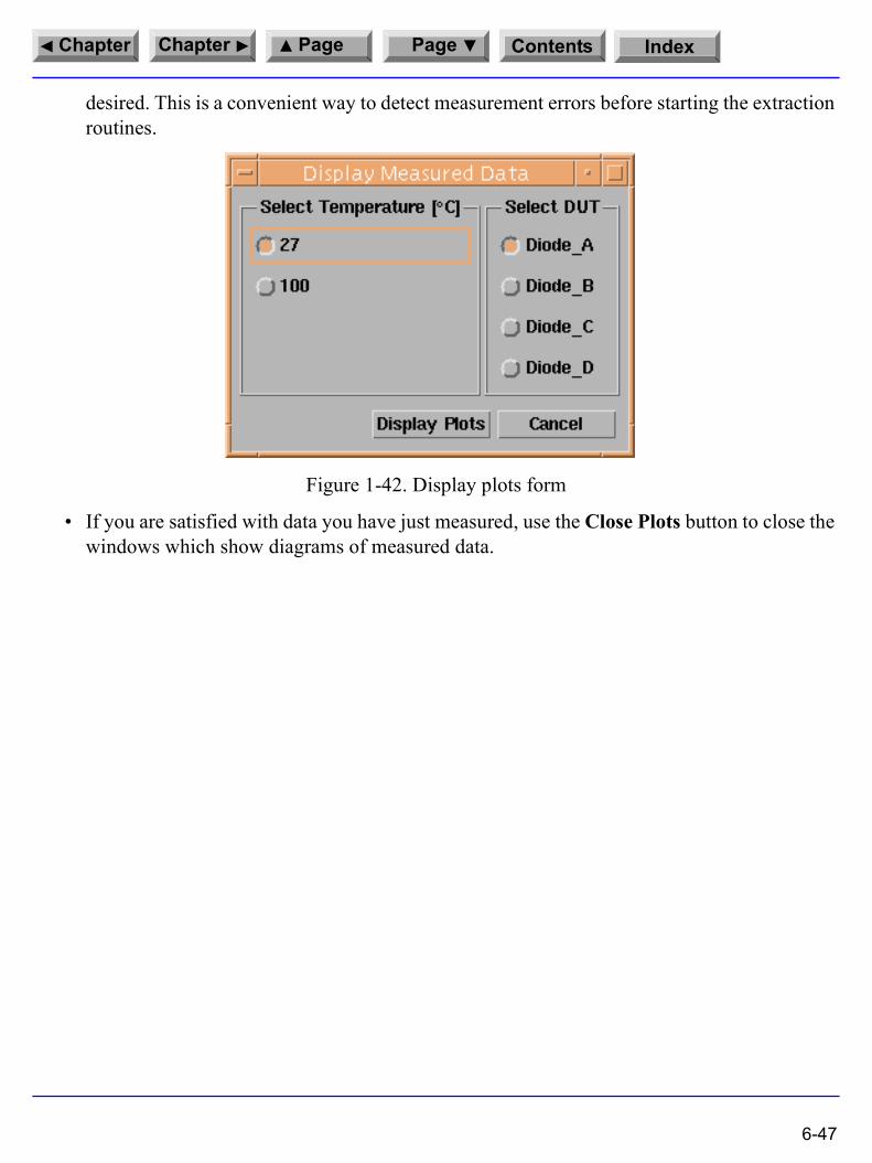
� To select devices to be measured at different temperatures: Click the Temp Meas button on the left side of the form. You will be prompted with a list of DUTs (Figure 1-38). Select the
6-44

Contents IndexPagePageChapterChapter
devices to be measured at those temperatures entered in the Temperature Setup form and click OK.
Figure 1-38. Form to define DUTs to be measured at temperatures entered on the Temperature Setup Form
Note: You cannot exclude a DUT to be measured at TNOM. All DUTs are measured automatically at that temperature. If you have entered one or more temperatures on the Temperature Setup form, the DUTs selected for temperature measurement are all measured at those temperatures. It is not possible to select a DUT for measurement at temperature T1 but not at another temperature T2.
� To start measurement of the devices: Click Measure and select the DUT(s) to be measured on the form that opens (Figure 1-39). You can select measurement temperature (if there is a temperature other than TNOM defined in the temperature setup form) as well as a specific DUT. Start measurement with the Measure button on that form. If measuring at elevated temperatures, be sure to wait until your devices are heated or cooled down to the desired temperature.
Figure 1-39. Measurement prompt
6-45

Contents IndexPagePageChapterChapter
� If you would like to clear data of some or all measured DUTs, use the Clear button. Select whether you would like to clear measured data of some or all DUT(s) at specified temperatures, see (Figure 1-40) and click Clear Data to delete measured data files.
Figure 1-40. Clear measured data
� Using the Synthesize button, you are able to simulate data from existing parameters. This synthesized data uses the voltages set on the Measurement Conditions form to generate �measurement� data from a known set of SPICE parameters. This might be especially useful to convert parameters of other models into BSIM4 parameters by loading the created �measurement data� into the extraction routines and extract BSIM4 parameters.
Figure 1-41. Dialog to synthesize measurement data
� For a glance at diagrams that are just been measured, use the Display Plots button. You will see a form to select which measured data set you would like to display. After choosing the plots you would like to see, use the Display Plots button on that form to open up the plots
6-46
Contents IndexPagePageChapterChapter
desired. This is a convenient way to detect measurement errors before starting the extraction routines.
Figure 1-42. Display plots form
� If you are satisfied with data you have just measured, use the Close Plots button to close the windows which show diagrams of measured data.
6-47

Contents IndexPagePageChapterChapter
Drain/Source � Bulk Diodes for DC Measurements
OptionsThis folder lets you define options for the appearance of the plot windows. You can choose whether you want a fixed window size or a variable size defined by the variables x- and y-size. You can change the window background color from black to white as well.
Extraction of Parameters for the BSIM4 ModelExtraction of parameters is done using the same look of the GUI as in measurement. The following Figure 1-43 shows the GUI used for extraction purposes. You can see the folders for tasks in the extraction process. Again ordered from left to right are folders for Notes, for measurement Information, to Initialize the extraction process, to Extract parameters from measurement data, to Display measured and simulated data to visualize the results of parameter extraction, to set some Environment conditions and to create a report in HTML format for publishing the parameters extracted together with some graphics of simulations using the parameters extracted.
Table 1-2. Test Structures for Drain/Source - Bulk Diodes
Category Shape Comment
BD/BS Perimeter Finger diode with large perimeter and small area (shown here for n-type devices)
BD/BS Area Area diode with large area and small perimeter (shown here for n-type devices)
6-48

Contents IndexPagePageChapterChapter
Figure 1-43. GUI for the Parameter Extraction Process
The top row of the GUI window contains buttons to perform file operations like Open, Save Settings, Export Settings and Import Settings. In the middle of the top row you�ll find the project name on blue background. To the right of the project name there is a Help button to open this manual. The Info button provides some information about the BSIM4 Modeling Package creators, Advanced Modeling Solutions. Far to the right you�ll find the Exit button to leave the GUI.
If you would like to open a project, you can select the project path and name in the Open Project form. Using the Export Settings button open the Export Extraction Settings form to choose path and name of the saved extraction settings file. These settings are the folders Notes, Initialize, Extract and HTML.
You are able to Import Extraction Settings by selecting the path and name of the saved extraction settings file inside the Import Extraction Settings form. This might be useful for example, if you have found a special extraction sequence full filling the need of your parameter extraction process best. You save those sequence by exporting the settings to a file and using this file as template for following extraction processes. Note: Importing extraction settings will overwrite the actual settings within the active extraction process!
The tasks to be performed are ordered from the left to the right side of the main window. They should be performed in this manner. Some of the forms are having default values for your convenience. If you are satisfied with the defaults, those forms could be left as they are. However, you are not bound to follow this order.
6-49
Contents IndexPagePageChapterChapter
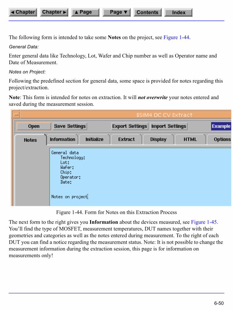
The following form is intended to take some Notes on the project, see Figure 1-44.
General Data:
Enter general data like Technology, Lot, Wafer and Chip number as well as Operator name and Date of Measurement.
Notes on Project:
Following the predefined section for general data, some space is provided for notes regarding this project/extraction.
Note: This form is intended for notes on extraction. It will not overwrite your notes entered and saved during the measurement session.
Figure 1-44. Form for Notes on this Extraction Process
The next form to the right gives you Information about the devices measured, see Figure 1-45. You�ll find the type of MOSFET, measurement temperatures, DUT names together with their geometries and categories as well as the notes entered during measurement. To the right of each DUT you can find a notice regarding the measurement status. Note: It is not possible to change the measurement information during the extraction session, this page is for information on measurements only!
6-50

Contents IndexPagePageChapterChapter
Figure 1-45. Information Page during Extraction
The folder Initialize (Figure 1-46) is intended to set initial conditions for parameter extraction. You�ll find a section �User Defined Defaults� which has fields for Process Parameters and Model Flags. Inside the field Process Parameters you enter process related parameters like the relative dielectric constant of the gate oxide, EPSROX. Advanced CMOS process generations are more and more making use of high-k gate dielectrics. Therefore, you can specify the relative dielectric constant of your process by changing EPSROX from 3.9 (default value for SiO2 gate dielectric).
6-51

Contents IndexPagePageChapterChapter
There are other process parameters to be specified on this page, including electrical, process or measured gate oxide thickness, TOXE, TOXP, TOXM, junction depth, doping concentrations, and sheet resistances. See the manual from UC Berkeley for details on model parameters /UCB manual/. Entering values into the fields starts a routine to check the values entered. This routine will flag an error message and change the color of the field whose parameter is given an unrealistic value. For example, if you enter �-3� into the EPSROX field, this field will be marked with red color and remains red until the value is corrected.
The section �Model Flags� is used to set BSIM4 model flags as defined in the UCB manual /UCB manual/. The fields only allow settings as defined in the BSIM4 model and are predefined to standard settings.
There is a field defining the symmetry of the drain and source areas. Check the appropriate box(es) if drain and source are processed using the same dose of implantation as well as the same geometry and therefore the parameters are equal for drain and source areas.
6-52

Contents IndexPagePageChapterChapter
Figure 1-46. Initialize folder to set initial conditions for extraction
To the left of the form, you�ll find buttons to Reset Model Parameters to known states. You can choose whether the parameters are reset to Circuit Defaults or to User Defined Defaults. Circuit Defaults refer to the defaults set inside BSIM4, resetting user defined parameters. In contrast, User Defined Defaults are resetting the parameters to the values the user has entered before starting an extraction process.
6-53

Contents IndexPagePageChapterChapter
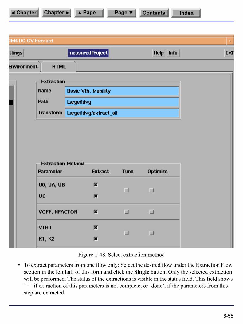
The next folder, Extract, defines the Extraction Flow for the devices. There is a standard extraction flow implemented, but you can change this flow if you find another one suiting your needs better than the default one.
Figure 1-47. Defining the extraction flow
The right half of this folder shows a field named Extraction and one named Extraction Method. The Extraction field shows the name for the selected extraction step together with path and transform used in this step. Under Extraction Method you are able to select whether the parameters are just extracted or, after extraction, tuned or optimized. The Extraction Method field is grouped, as shown in Figure 1-48. For example, the parameter UC is extracted in sequence with U0, UA and UB inside the same parameter group. The tuner or optimizer feature can only be invoked for all parameters in that group, because there is a great influence on each other.
6-54
Contents IndexPagePageChapterChapter
Figure 1-48. Select extraction method
� To extract parameters from one flow only: Select the desired flow under the Extraction Flow section in the left half of this form and click the Single button. Only the selected extraction will be performed. The status of the extractions is visible in the status field. This field shows � - � if extraction of this parameters is not complete, or �done�, if the parameters from this step are extracted.
6-55

Contents IndexPagePageChapterChapter
� To go through the extraction process in one step after the other, click Step by Step. You will be prompted after each single step.
� To automatically extract all parameters using the extraction flows listed under the Extraction Flow section: Click Automatic. The programmed Extraction Flow will be extracting all parameters defined in the active extraction flow list. The programmed extraction flow has to begin with the step: Reset Parameters, otherwise you will get an error message, see the following figure.
Figure 1-49. Warning message, if the extraction flow doesn�t begin with Reset Parameters
In case you would start an extraction of some parameters after you already have extracted some other parameters, you are not able to start from the beginning without resetting all parameters, including the ones already extracted. To re-extract or to optimize one parameter after some other parameters are already extracted, simply add the desired step in the extraction flow list on a place further down the list. In that case, the extraction process uses the parameters already extracted during an earlier step in the extraction process and you overcome the reset parameter step.
� All warnings and errors during the extraction process are written to the failure log, which is opened using the Failure Log button. Note: The contents of the Failure Log window doesn�t contain all the warnings written to the IC-CAP status window. Only the warnings and errors regarding parameter extraction are directed to the Failure Log.
Figure 1-50. Extraction Failure log window
6-56
Contents IndexPagePageChapterChapter
� If you would like to clear the status of extraction, use the Clear Status button to reset the status field to the right of each step in the Extraction Flow to �-�.
� The button Simulate All starts simulating the circuit as defined in IC-CAP.
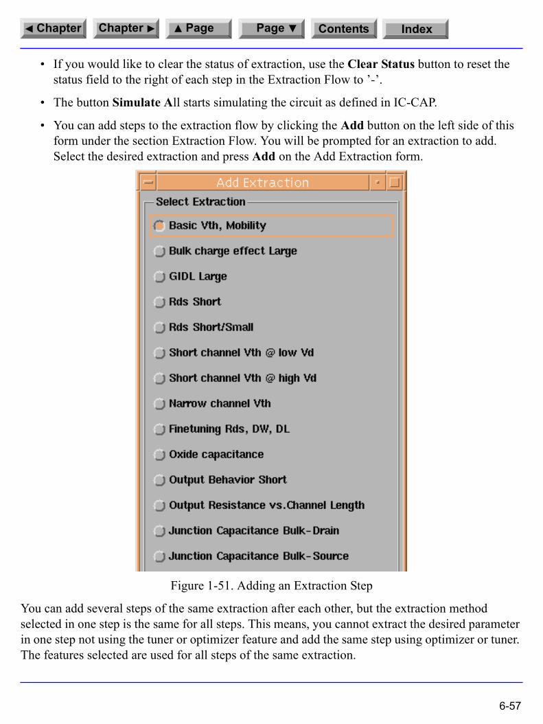
� You can add steps to the extraction flow by clicking the Add button on the left side of this form under the section Extraction Flow. You will be prompted for an extraction to add. Select the desired extraction and press Add on the Add Extraction form.
Figure 1-51. Adding an Extraction Step
You can add several steps of the same extraction after each other, but the extraction method selected in one step is the same for all steps. This means, you cannot extract the desired parameter in one step not using the tuner or optimizer feature and add the same step using optimizer or tuner. The features selected are used for all steps of the same extraction.
6-57

Contents IndexPagePageChapterChapter
� Change the extraction flow by using the Move Up or Move Down buttons to move a selected extraction routine one step up or down.
� The Default button restores the order and number of parameter extractions as it was in the beginning of a project.
� To delete a step: Use the Delete button. Note: You cannot delete the first (Reset Parameters) and the last (Save Parameters) step inside an extraction flow.
� To export the extracted parameters: Use the Export button under Parameters. You will be prompted whether you would like to export the parameters in an IC-CAP-readable format or as an extracted SPICE deck with the extension .lib for use in any SPICE compatible simulator. You must specify the path and the name of the exported parameter file.
Figure 1-52. Export Model Parameters
6-58

Contents IndexPagePageChapterChapter
� There is a button provided for Import of parameters, e.g. from an earlier project. You will receive a warning message, stating that importing parameters will overwrite the actual model parameters in IC-CAP.
Figure 1-53. Import Model Parameters
The next folder to the right, Display, is used to display diagrams of measured and simulated setups together to view the results of parameter extraction. It has sections for DC Transistor, Capacitance, and DC Diode behavior. Within those sections, there are fields representing diagrams and their relevant parameters. By clicking on one of the predefined lines, simulation of the selected setup using the voltages defined in �Measurement Conditions� takes place and is displayed in diagrams.
Note: The environmental settings regarding size and background color are effective in displaying the diagrams using this folder.
6-59

Contents IndexPagePageChapterChapter
Figure 1-54. Displaying simulation results using the parameters extracted
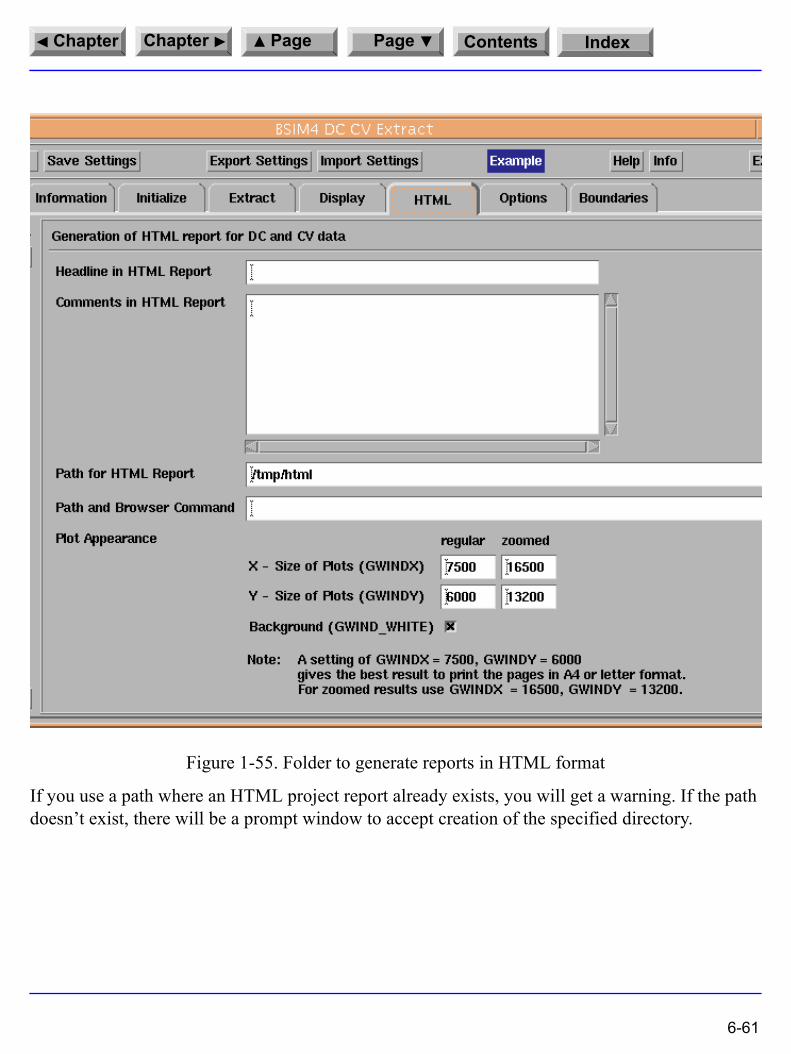
The folder HTML is used to generate a report file in HTML format. You can define a headline and comments for the report, specify the path to save the report as well as the command to start the browser. You can also define the size of plots and the diagram background as it appears in the HTML report.
6-60
Contents IndexPagePageChapterChapter
Figure 1-55. Folder to generate reports in HTML format
If you use a path where an HTML project report already exists, you will get a warning. If the path doesn�t exist, there will be a prompt window to accept creation of the specified directory.
6-61

Contents IndexPagePageChapterChapter
The following figures are showing part of a generated HTML report. This report could be published over the intranet for use inside your company or over the web for use of customers.
6-62

Contents IndexPagePageChapterChapter
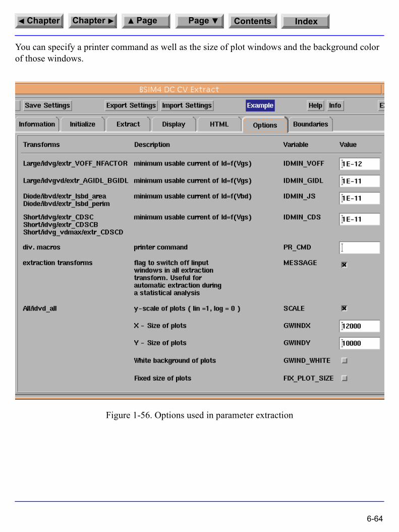
The folder Options lets you define some environmental conditions used in extraction. There are predefined values for the variables, you are able to change those variables or accept the values.
Using those variables you can define a minimum usable current for extraction. The purpose of these variables is to cut out noisy current measurements by defining the lower limit of currents used for extraction of different parameters.
6-63
Contents IndexPagePageChapterChapter
You can specify a printer command as well as the size of plot windows and the background color of those windows.
Figure 1-56. Options used in parameter extraction
6-64
Contents IndexPagePageChapterChapter
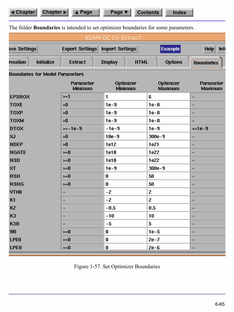
The folder Boundaries is intended to set optimizer boundaries for some parameters.
Figure 1-57. Set Optimizer Boundaries
6-65
Contents IndexPagePageChapterChapter
Displayed is part of the Boundaries folder. On the left side, you can see the parameter to be optimized. The following columns display the minimum for the named parameter (the parameter�s reasonable physical minimum), an optimizer minimum and maximum column, followed by the parameter�s maximum, if a reasonable one exists. The white fields let you enter optimizer settings fitting your process needs. You can export these settings for future extractions using the Export button inside the Boundaries field to the left. If you have exported boundaries, you can use those boundaries by clicking the Import button.
The buttons OK and Defaults refer to accepting the optimizer boundaries for just this extraction session respective to re-establish the default boundaries which come with the BSIM4 Modeling Package.
References:[1] BSIM4.0.0 Manual, University of California at Berkeley, Copyright © 2001 The Regents of
the University of California. See the web site of the device research group at UCB. You can download the manual from the Internet, using the following Web address : http://www-device.eecs.berkeley.edu:80/~bsim3/bsim4_get.html
Acknowledgements:The BSIM4 model was developed by the UC Berkeley BSIM Research Group.
6-66