Embed Size (px)
Citation preview
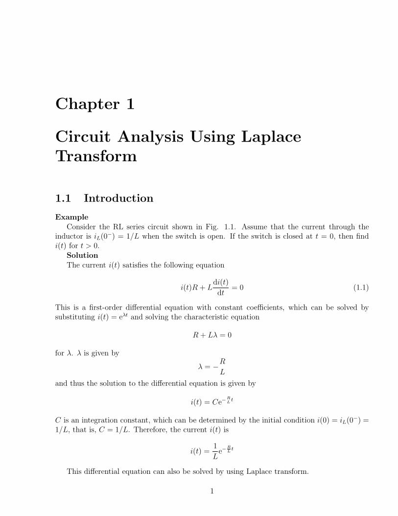
Chapter 1
Circuit Analysis Using LaplaceTransform
1.1 Introduction
ExampleConsider the RL series circuit shown in Fig. 1.1. Assume that the current through the
inductor is iL(0−) = 1/L when the switch is open. If the switch is closed at t = 0, then findi(t) for t > 0.
SolutionThe current i(t) satisfies the following equation
i(t)R + Ldi(t)
dt= 0 (1.1)
This is a first-order differential equation with constant coefficients, which can be solved bysubstituting i(t) = eλt and solving the characteristic equation
R + Lλ = 0
for λ. λ is given by
λ = −R
L
and thus the solution to the differential equation is given by
i(t) = Ce−RL
t
C is an integration constant, which can be determined by the initial condition i(0) = iL(0−) =1/L, that is, C = 1/L. Therefore, the current i(t) is
i(t) =1
Le−
RL
t
This differential equation can also be solved by using Laplace transform.
1

2 CHAPTER 1. CIRCUIT ANALYSIS USING LAPLACE TRANSFORM
1.2 Review of Laplace Transform
DefinitionLet f(t) be a given function defined for t ≥ 0. Then, its Laplace transform is defined as
F (s) = Lf(t) =∫ ∞
0e−stf(t)dt
which shows that the function f(t) in time domain is transformed to the function F (s) in sor complex frequency domain by Laplace transform operation. F (s) and Lf(t) is called theLaplace transform of f(t), and the original function f(t) is called the inverse transform orinverse of F (s), denoted by L−1F (s), that is,
f(t) = L−1F (s)
Properties
1. Linearity
Laf(t) + bg(t) = aLf(t) + bLg(t)
Laf(t) + bg(t) =∫ ∞
0e−st[af(t) + bg(t)]dt
= a∫ ∞
0e−stf(t)dt + b
∫ ∞
0e−stg(t)dt
= aLf(t) + bLg(t) (1.2)
2. First Shifting Theorem
Leatf(t) = F (s − a)eatf(t) = L−1F (s − a) (1.3)
F (s − a) =∫ ∞
0e−(s−a)tf(t)dt
=∫ ∞
0e−st[eatf(t)]dt
= Leatf(t) (1.4)
3. Transform of Derivatives
Lf (n)(t) = snLf(t) − sn−1f(0) − sn−2f ′(0) − · · · − sf (n−2)(0) − f (n−1)(0)
Case n = 1

1.2. REVIEW OF LAPLACE TRANSFORM 3
Lf ′(t) =∫ ∞
0e−stf ′(t)dt
=∫ ∞
0e−stdf(t)
=[e−stf(t)
]∞0
+ s∫ ∞
0e−stf(t)dt
= sLf(t) − f(0) (1.5)
d(uv) = vdu + udv
uv =∫
d(uv) =∫
vdu +∫
udv∫
udv = uv −∫
vdu
Case n = 2
Lf ′′(t) = sLf ′(t) − f ′(0)= s[sLf(t) − f(0)] − f ′(0)= s2Lf(t) − sf(0) − f ′(0) (1.6)
4. Transform of Integral
L∫ t
0f(τ)dτ
=
1
sF (s)
∫ t
0f(τ)dτ = L−1
1
sF (s)
(1.7)
F (s) = Lf(t) = L
(∫ t
0f(τ)dτ
)′
= sL∫ t
0f(τ)dτ
−∫ 0
0f(τ)dτ
= sL∫ t
0f(τ)dτ
(1.8)
which implies that L∫ t
0 f(τ)dτ
= 1sF (s).
5. Initial Value Theorem
f(0) = lims→∞
sF (s)
6. Final Value Theorem
f(∞) = limt→∞
f(t) = lims→0
sF (s)

4 CHAPTER 1. CIRCUIT ANALYSIS USING LAPLACE TRANSFORM
7. Table of Lapace Transforms
unit impulse δ(t) 1unit step 1(t) 1
s
unit ramp t 1s2
unit acceleration t2
21s3
n-th order ramp tn
n!1
sn+1
exponential e−at 1s+a
n-th order exponential tn
n!e−at 1
(s+a)n+1
sine sin ωt ωs2+ω2
cosine cos ωt ss2+ω2
damped sine e−at sin ωt ω(s+a)2+ω2
damped cosine e−at cos ωt s+a(s+a)2+ω2
1.3 Differential Equations
Consider a second-order differential equation with constant coefficients:
y′′(t) + ay
′(t) + by(t) = u(t), y(0) = K1, y
′(0) = K2 (1.9)
with constant a and b. Here u(t) is the input (driving force and current source or voltagesource) applied to the (mechanical and electrical) system and y(t) is the output (response) ofthe system. Laplace transform method involves the following three steps:
1. Taking the transform on both sides of (1.9) gives
[s2Y (s) − sy(0) − y′(0)] + a[sY (s) − y(0)] + bY (s) = U(s)
which is called the subsidiary equation. Collecting Y -terms, we have
(s2 + as + b)Y (s) = (s + a)y(0) + y′(0) + U(s)
2. Solving the subsidiary equation algebraically for Y (s) produces
Y (s) = [(s + a)y(0) + y′(0)]Q(s) + U(s)Q(s) (1.10)
where Q(s) is transfer function and is defined as
Q(s) =1
s2 + as + b
If y(0) = y′(0) = 0, then (1.10) becomes Y (s) = U(s)Q(s). Thus, Q(s) is the quotient
Q(s) =Y (s)
U(s)=
LoutputLinput
which explains the name of Q(s).

1.4. PARTIAL FRACTIONS 5
3. Using partial fractions, reduce (1.10) to a sum of terms whose inverses can be found fromthe table, so that the solution y(t) = L−1Y (s) of (1.9) is obtained.
Example
Solve the differential equation (1.1), that is,
i(t)R + Ldi(t)
dt= 0, i(0) = 1/L
Taking the Laplace transform on both sides yields
I(s)R + LsI(s) − 1 = 0
Solving this equation gives
I(s) =1
Ls + R=
1L
s + RL
Taking the inverse on both sides produces
i(t) =1
Le−
RL
t
1.4 Partial Fractions
The Solution Y (s) of a subsidiary equation of a differential equation usually comes out as aquotient of two polynomials,
Y (s) =P (s)
Q(s)
In order to find y(t) by taking the inverse of Y (s), it is better to write Y (s) as a sum of partialfractions. The form of the partial fractions depends on the types of factors in the product formof Q(s). We often encounter the following cases.
1. Unrepeated factors (s − a1)(s − a2)
Y (s) =A1
s − a1
+A2
s − a2
2. Repeated factors (s − a)2
Y (s) =A1
s − a+
A2
(s − a)2
3. Complex factors [s − (α + jβ)][s − (α − jβ)]
Y (s) =As + B
[s − (α + jβ)][s − (α − jβ)]=
As + B
(s − α)2 + β2
6 CHAPTER 1. CIRCUIT ANALYSIS USING LAPLACE TRANSFORM
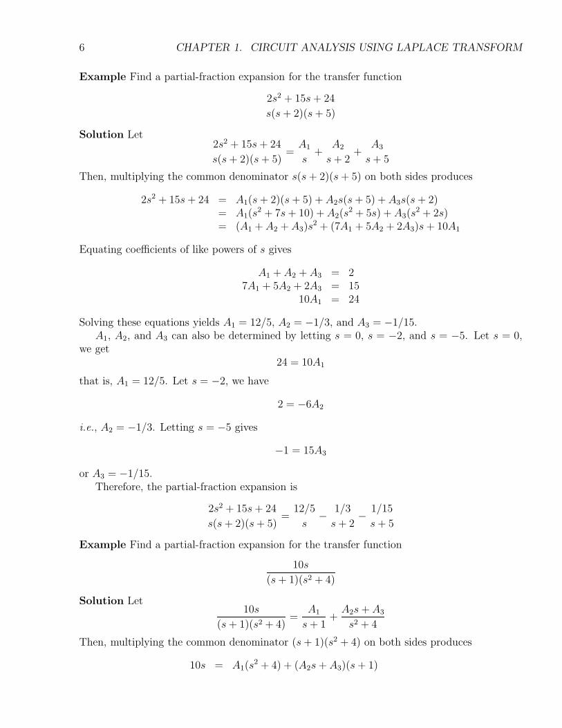
Example Find a partial-fraction expansion for the transfer function
2s2 + 15s + 24
s(s + 2)(s + 5)
Solution Let2s2 + 15s + 24
s(s + 2)(s + 5)=
A1
s+
A2
s + 2+
A3
s + 5
Then, multiplying the common denominator s(s + 2)(s + 5) on both sides produces
2s2 + 15s + 24 = A1(s + 2)(s + 5) + A2s(s + 5) + A3s(s + 2)= A1(s
2 + 7s + 10) + A2(s2 + 5s) + A3(s
2 + 2s)= (A1 + A2 + A3)s
2 + (7A1 + 5A2 + 2A3)s + 10A1
Equating coefficients of like powers of s gives
A1 + A2 + A3 = 27A1 + 5A2 + 2A3 = 15
10A1 = 24
Solving these equations yields A1 = 12/5, A2 = −1/3, and A3 = −1/15.A1, A2, and A3 can also be determined by letting s = 0, s = −2, and s = −5. Let s = 0,
we get24 = 10A1
that is, A1 = 12/5. Let s = −2, we have
2 = −6A2
i.e., A2 = −1/3. Letting s = −5 gives
−1 = 15A3
or A3 = −1/15.Therefore, the partial-fraction expansion is
2s2 + 15s + 24
s(s + 2)(s + 5)=
12/5
s− 1/3
s + 2− 1/15
s + 5
Example Find a partial-fraction expansion for the transfer function
10s
(s + 1)(s2 + 4)
Solution Let10s
(s + 1)(s2 + 4)=
A1
s + 1+
A2s + A3
s2 + 4
Then, multiplying the common denominator (s + 1)(s2 + 4) on both sides produces
10s = A1(s2 + 4) + (A2s + A3)(s + 1)

1.5. ELECTRICAL ELEMENT MODELS 7
= A1(s2 + 4) + (A2s
2 + A2s + A3s + A3)= (A1 + A2)s
2 + (A2 + A3)s + 4A1 + A3
Equating coefficients of like powers of s gives
A1 + A2 = 0A2 + A3 = 10
4A1 + A3 = 0
Solving these equations yields A1 = −2, A2 = 2, and A3 = 8.Therefore, the partial-fraction expansion is
10s
(s + 1)(s2 + 4)= − 2
s + 1+
2s + 8
s2 + 4
Example Find a partial-fraction expansion for the transfer function
4 − 2s
(s2 + 1)(s − 1)2
Solution Let4 − 2s
(s2 + 1)(s − 1)2=
A1s + A2
s2 + 1+
A3
s − 1+
A4
(s − 1)2
Then, multiplying the common denominator (s2 + 1)(s − 1)2 on both sides produces
4 − 2s = (A1s + A2)(s − 1)2 + A3(s2 + 1)(s − 1) + A4(s
2 + 1)= (A1s + A2)(s
2 − 2s + 1) + A3(s3 − s2 + s − 1) + A4(s
2 + 1)= (A1s
3 + A2s2 − 2A1s
2 − 2A2s + A1s + A2) + A3(s3 − s2 + s − 1) + A4(s
2 + 1)= (A1 + A3)s
3 + (A2 − 2A1 − A3 + A4)s2 + (−2A2 + A1 + A3)s + A2 − A3 + A4
Equating coefficients of like powers of s gives
A1 + A3 = 0 A1 = −A3
A2 − 2A1 − A3 + A4 = 0 A4 = −A3 − 1−2A2 + A1 + A3 = −2 A2 = 1
A2 − A3 + A4 = 4 A3 = −2
Solving these equations yields A1 = 2, A2 = 1, A3 = −2, and A4 = 1. Therefore, the partial-fraction expansion is
4 − 2s
(s2 + 1)(s − 1)2=
2s + 1
s2 + 1− 2
s − 1+
1
(s − 1)2
1.5 Electrical Element Models
Resistorv(t) = Ri(t) V (s) = RI(s)

8 CHAPTER 1. CIRCUIT ANALYSIS USING LAPLACE TRANSFORM
Capacitor
i(t) = Cdv(t)
dtI(s) = CsV (s) − CVC(0) or V (s) =
1
CsI(s) +
1
sVC(0)
Inductor
v(t) = Ldi(t)
dtV (s) = LsI(s) − LiL(0) or I(s) =
V (s)
Ls+
1
siL(0)
1.6 Analysis of Electrical Network by Laplace Transform
1. Determine the initial conditions.
2. Draw equivalent circuit in s-domain.
3. Write loop voltage equations or node current equations.
4. Solve the resulting algebraic equations for unknown variables.
5. Reduce the equations for the unknowns to a sum of terms by partial fractions.
6. Take the inverses and find the expressions for the unknowns in time domain.
Example
Find the current in the following circuit by Laplace transform, assuming that all initialconditions are zero.

1.6. ANALYSIS OF ELECTRICAL NETWORK BY LAPLACE TRANSFORM 9
SolutionApplying Laplace transform yields the following circuit:
By Kirchhoff’s voltage law, we get
I(s) =5
s+1
6 + s + 8s
=5s
(s + 1)(s2 + 6s + 8)
=5s
(s + 1)(s + 2)(s + 4)
Now let5s
(s + 1)(s + 2)(s + 4)=
A1
s + 1+
A2
s + 2+
A3
s + 4
Multiplying the common denominator (s + 1)(s + 2)(s + 4) on both sides gives
5s = A1(s + 2)(s + 4) + A2(s + 1)(s + 4) + A3(s + 1)(s + 2)
Let s = −1, we get −5 = 3A1 or A1 = −5/3.Let s = −2, we have −10 = −2A2 or A2 = 5.Let s = −4, we obtain −20 = 6A3 or A3 = −10/3.Therefore,
I(s) = − 5/3
s + 1+
5
s + 2− 10/3
s + 4
Taking inverse on both sides yields
i(t) = −5
3e−t + 5e−2t − 10
3e−4t
ExampleConsider the following RLC parallel circuit with R = 3/4Ω, C = 1/3F , L = 1H, vC(0−) =
2V , and iL(0−) = 0. The switch is closed at t = 0. Find v(t) for t > 0.
Solution

10 CHAPTER 1. CIRCUIT ANALYSIS USING LAPLACE TRANSFORM
Taking Laplace to transform, we get the equivalent circuit in s domain as follows
which is equivalent to the circuit to the right by Norton Theorem. By Kirchhoff’s currentlaw, we get
I = IC + IR + IL
which is equivalent to
2C = sCV (s) +1
RV (s) +
1
sLV (s)
Solving for V (s) produces
V (s) =2C
sC + 1R
+ 1sL
=23
s3
+ 43
+ 1s
=2s
s2 + 4s + 3
=2s
(s + 1)(s + 3)
Now, let us take a partial-fraction expansion. Set
2s
(s + 1)(s + 3)=
A1
s + 1+
A2
s + 3
Multiplying the common denominator (s + 1)(s + 3) on both sides gives
2s = A1(s + 3) + A2(s + 1)
Setting s = −1 gives A1 = −1, setting s = −3 gives A2 = 3. Therefore, we get
V (s) = − 1
s + 1+ 3
1
s + 3
Taking inverse on both sides produces
v(t) = 3e−3t − e−t
ExampleConsider the following electrical circuit with R = 30Ω, L = 10mH, C = 50µF , and
is(t) =
−50mA t ≤ 050mA t > 0

1.6. ANALYSIS OF ELECTRICAL NETWORK BY LAPLACE TRANSFORM 11
Find the current through the inductor by Laplace transform.
SolutionFirst let us determine the initial condition for the voltage across the capacitor C. Note that
at t = 0− the circuit reaches a steady-state, so iL(0−) = 0 and
VC(0−) = is(0−)R = (−50mA)(30Ω) = −1.5V
Applying Laplace transform gives the following circuit
By Kirchhoff’s voltage law, I(s) can be found from
I(s)(R + sL +
1
sC
)= RIs(s) −
vC(0)
s
that is,
I(s)(30 + 10 × 10−3s +
1
50 × 10−6s
)= 30 × 50 × 10−3 1
s− −1.5
sor
I(s)(30 +
s
100+
20000
s
)=
3
s
Multiplying 100s on both sides produces
I(s)(3000s + s2 + 2000000) = 300
that is,
I(s) =300
(3000s + s2 + 2000000)=
300
(s + 1000)(s + 2000)
Let300
(s + 1000)(s + 2000)=
A1
s + 1000+
A2
s + 2000
Multiplying (s + 1000)(s + 2000) on both sides of the above equation gives
300 = A1(s + 2000) + A2(s + 1000)

12 CHAPTER 1. CIRCUIT ANALYSIS USING LAPLACE TRANSFORM
Letting s = −1000 gives A1 = 0.3 and s = −2000 gives A2 = −0.3. Then, we get
I(s) =0.3
s + 1000− 0.3
s + 2000
Taking inverse on both sides gives
i(t) = 0.3e−1000t − 0.3e−2000t
ExampleConsider the following electrical circuit with R = 2Ω, L = 1H, C = 1F , and
vs(t) =
4V t ≤ 04e−tV t > 0
Find v0(t) by Laplace transform.
SolutionFirst we need to determine the initial conditions. Note that the circuit reaches its steady-
state condition at t = 0−, that is, the current through the capacitor is zero and the voltageacross the inductor is zero. Therefore, we get
iL(0−) =vs(0
−)
2Ω + 2Ω=
4V
4Ω= 1A
vC(0−) = v0(0−) = iL(0−)(2Ω) = (1A)(2Ω) = 2V
Then, taking Laplace transform produces the following circuit in s domain.
By writing mesh equations for I1 and I2, we have
0 =4
s + 1− 2I1 −
1
s(I1 − I2) −
2
s
0 =2
s− 1
s(I2 − I1) − (s + 2)I2 + 1
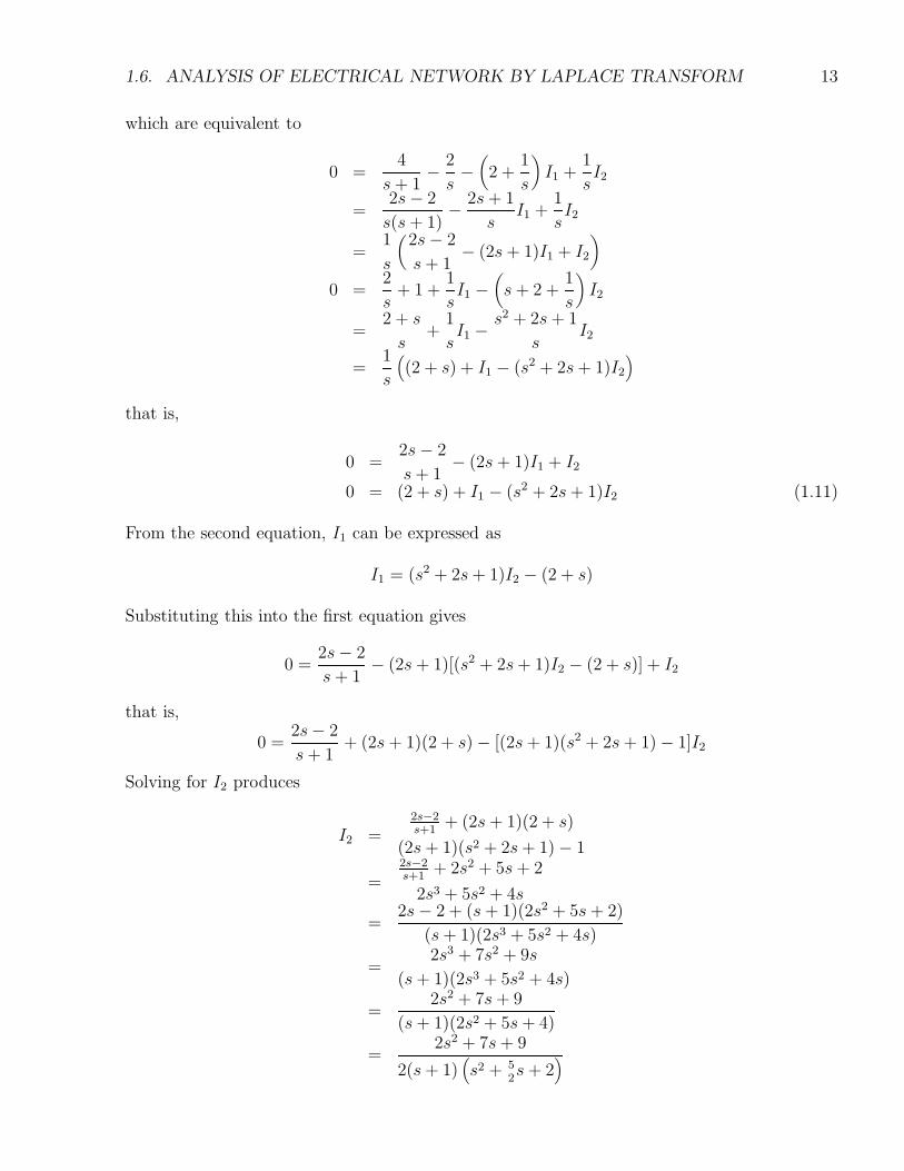
1.6. ANALYSIS OF ELECTRICAL NETWORK BY LAPLACE TRANSFORM 13
which are equivalent to
0 =4
s + 1− 2
s−(2 +
1
s
)I1 +
1
sI2
=2s − 2
s(s + 1)− 2s + 1
sI1 +
1
sI2
=1
s
(2s − 2
s + 1− (2s + 1)I1 + I2
)
0 =2
s+ 1 +
1
sI1 −
(s + 2 +
1
s
)I2
=2 + s
s+
1
sI1 −
s2 + 2s + 1
sI2
=1
s
((2 + s) + I1 − (s2 + 2s + 1)I2
)
that is,
0 =2s − 2
s + 1− (2s + 1)I1 + I2
0 = (2 + s) + I1 − (s2 + 2s + 1)I2 (1.11)
From the second equation, I1 can be expressed as
I1 = (s2 + 2s + 1)I2 − (2 + s)
Substituting this into the first equation gives
0 =2s − 2
s + 1− (2s + 1)[(s2 + 2s + 1)I2 − (2 + s)] + I2
that is,
0 =2s − 2
s + 1+ (2s + 1)(2 + s) − [(2s + 1)(s2 + 2s + 1) − 1]I2
Solving for I2 produces
I2 =2s−2s+1
+ (2s + 1)(2 + s)
(2s + 1)(s2 + 2s + 1) − 1
=2s−2s+1
+ 2s2 + 5s + 2
2s3 + 5s2 + 4s
=2s − 2 + (s + 1)(2s2 + 5s + 2)
(s + 1)(2s3 + 5s2 + 4s)
=2s3 + 7s2 + 9s
(s + 1)(2s3 + 5s2 + 4s)
=2s2 + 7s + 9
(s + 1)(2s2 + 5s + 4)
=2s2 + 7s + 9
2(s + 1)(s2 + 5
2s + 2
)
14 CHAPTER 1. CIRCUIT ANALYSIS USING LAPLACE TRANSFORM
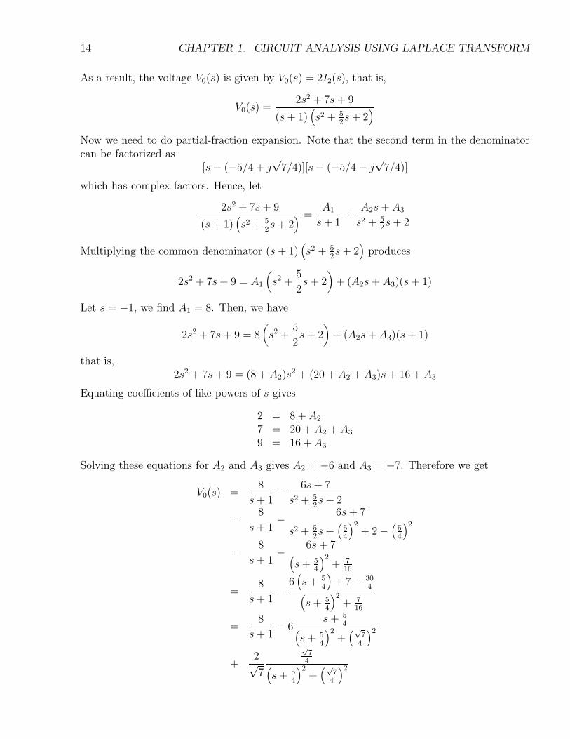
As a result, the voltage V0(s) is given by V0(s) = 2I2(s), that is,
V0(s) =2s2 + 7s + 9
(s + 1)(s2 + 5
2s + 2
)
Now we need to do partial-fraction expansion. Note that the second term in the denominatorcan be factorized as
[s − (−5/4 + j√
7/4)][s − (−5/4 − j√
7/4)]
which has complex factors. Hence, let
2s2 + 7s + 9
(s + 1)(s2 + 5
2s + 2
) =A1
s + 1+
A2s + A3
s2 + 52s + 2
Multiplying the common denominator (s + 1)(s2 + 5
2s + 2
)produces
2s2 + 7s + 9 = A1
(s2 +
5
2s + 2
)+ (A2s + A3)(s + 1)
Let s = −1, we find A1 = 8. Then, we have
2s2 + 7s + 9 = 8(s2 +
5
2s + 2
)+ (A2s + A3)(s + 1)
that is,2s2 + 7s + 9 = (8 + A2)s
2 + (20 + A2 + A3)s + 16 + A3
Equating coefficients of like powers of s gives
2 = 8 + A2
7 = 20 + A2 + A3
9 = 16 + A3
Solving these equations for A2 and A3 gives A2 = −6 and A3 = −7. Therefore we get
V0(s) =8
s + 1− 6s + 7
s2 + 52s + 2
=8
s + 1− 6s + 7
s2 + 52s +
(54
)2+ 2 −
(54
)2
=8
s + 1− 6s + 7(s + 5
4
)2+ 7
16
=8
s + 1−
6(s + 5
4
)+ 7 − 30
4(s + 5
4
)2+ 7
16
=8
s + 1− 6
s + 54(
s + 54
)2+(√
74
)2
+2√7
√7
4(s + 5
4
)2+(√
74
)2

1.6. ANALYSIS OF ELECTRICAL NETWORK BY LAPLACE TRANSFORM 15
Taking inverse on both sides gives
vo(t) = 8e−t − 6e−54t cos
(√7
4t
)
+2√7e−
54t sin
(√7
4t
)
ExampleConsider the following half-wave rectifier circuit with an inductive R − L load. vi =
Vmax sin ωt =√
2V sin ωt. Find the current i(t) through the load.
SolutionDuring the positive half cycle of the input voltage, the diode is forward biased and so
current flow commences as the supply voltage goes positive. The presence of L delays thecurrent change. The current continues to flow at the end of the positive half cycle because ofthis inductance. The diode remains on and the load sees the negative supply voltage until thecurrent decays to zero. This process can be analyzed mathematically as follows.
By writing Kirchhoff voltage equation, we get
vi = VL + VR
that is,
Vmax sin ωt = Ldi(t)
dt+ Ri(t)
Note that i(0) = 0. Taking the Laplace transform on both sides of the above equation gives
ωVmax
s2 + ω2= sLI(s) + RI(s)
Solving for I(s) produces
I(s) =ωVmax
(s2 + ω2)(R + sL)=
ωVmax
L(s2 + ω2)(s + RL)
Let a = RL. Then, it follows that
I(s) =ωVmax
L(s2 + ω2)(s + a)=
ωVmax
L
1
(s2 + ω2)(s + a)
Let1
(s2 + ω2)(s + a)=
As + B
(s2 + ω2)+
C
s + a

16 CHAPTER 1. CIRCUIT ANALYSIS USING LAPLACE TRANSFORM
Multiplying the common denominator (s2 + ω2)(s + a) yields
1 = (As + B)(s + a) + C(s2 + ω2)= As2 + Aas + Bs + Ba + Cs2 + Cω2
= (A + C)s2 + (Aa + B)s + Ba + Cω2
By equating coefficients of like powers of s, we get
A + C = 0Aa + B = 0
Ba + Cω2 = 1
The first equation gives C = −A and the second gives B = −aA. Substituting both C = −Aand B = −aA into the third equation produces
−a2A − ω2A = 1
that is,
A = − 1
a2 + ω2
So, we have C = 1a2+ω2 and B = a
a2+ω2 .Therefore, I(s) is given by
I(s) =ωVmax
L
− 1a2+ω2 s + a
a2+ω2
s2 + ω2+
1a2+ω2
(s + a)
=ωVmax
L(a2 + ω2)
− s
s2 + ω2+
a
s2 + ω2+
1
(s + a)
=ωVmax
L(R2
L2 + ω2)
− s
s2 + ω2+
a
s2 + ω2+
1
(s + a)
=ωLVmax
R2 + (ωL)2)
− s
s2 + ω2+
a
ω
ω
s2 + ω2+
1
(s + a)
Taking the inverse transform gives
i(t) =ωLVmax
R2 + (ωL)2)
− cos ωt +
a
ωsin ωt + e−at
=ωLVmax
R2 + (ωL)2)
a
ωsin ωt − cos ωt + e−at
=ωLVmax
Z2
a
ωsin ωt − cos ωt + e−at
with Z =√
R2 + (ωL)2.Now let
a
ωsin ωt − cos ωt = A sin(ωt − φ)
Then, we havea
ωsin ωt − cos ωt = A sin ωt cos φ − A cos ωt sin φ

1.6. ANALYSIS OF ELECTRICAL NETWORK BY LAPLACE TRANSFORM 17
By letting ωt = 0 and ωt = π2, we get
−1 = −A sin φa
ω= A cos φ
which implies that
tanφ =ω
a=
ωL
R
and
A2 = 1 +a2
ω2= 1 +
R2
(ωL)2=
(ωL)2 + R2
(ωL)2=
Z2
(ωL)2
Hence,
A =Z
ωL
Therefore, we have derived the following.
i(t) =ωLVmax
Z2
Z
ωLsin(ωt − φ) + e−at
=Vmax
Z
ωL
Z
Z
ωLsin(ωt − φ) +
ωL
Ze−at
=Vmax
Z
sin(ωt − φ) +
ωL
Ze−at
Recall that A sin φ = 1 with A = ZωL
. Hence
sin φ =1
A=
ωL
Z
Therefore, the current takes the form of
i(t) =Vmax
Z
sin(ωt − φ) + sin φe−
RL
t
Now let us calculate the time at which the current decays to zero. To this end, assume thatthe current will become zero at ωt = β, that is,
Vmax
Z
sin(β − φ) + sin φe−
RL
βω
= 0
The solution to this equation has no analytical form, so we have to use the numerical methodto solve for β.
This differential equation can also be solved as follows:Let i(t) = if (t) + in(t) where if (t) is force response or steady-state response and in(t) is
natural response or zero-state response.if(t) is determined by the phasor analysis as
if (t) =vi(t)
Z=
Vmax
Zsin(ωt − φ)
where Z =√
R2 + (Lω)2 and φ = tan−1 LωR
.

18 CHAPTER 1. CIRCUIT ANALYSIS USING LAPLACE TRANSFORM
in(t) is determined by in(t) = Ae−tτ with τ = L
R.
Then, we have
i(t) =Vmax
Zsin(ωt − φ) + Ae−
tτ
where A is determined from the initial condition i(0) = 0, i.e.
A =Vmax
Zsin φ

Chapter 2
Thyristors
A thyristor is a four-layer seniconductor device of PNPN structure with three PN-junctions. Ithas three terminals: anode, cathode, and gate. The thyristor symbol and the sectional view ofthree PN-junctions are shown in the figure below.
There are several members of the thyristor family. The more commonly used thyristors are
1. silicon-controlled rectifiers (SCRs)
2. gate-turn-off (GTO) thyristors
3. bi-directional triode thyristors (TRIACs)
2.1 Silicon-Controlled Rectifiers
The SCR is a four-layer PNPN semiconductor device. A dc voltage is applied to the SCR acrossthe anode and cathode through a resistor RA and another dc voltage source is connected tothe gate through a switch S and a resistor RG, as shown in the figure below. Assume that theswitch is open initially.
19

20 CHAPTER 2. THYRISTORS
In order to see how the SCR works, let us divide the middle PN regions along the dottedline, and model the SCR by a PNP transistor and an NPN transistor (two transistor model).
S is open initially
In this case, there is no gate current, only small leakage current flows from anode to cathodeand no conduction can take place. The SCR is said to be in the forward blocking or off-statecondition, and the leakage current is known as off-state or forward leakage current ID.
If the anode-to-cathode voltage VAK is increased to a sufficiently large value VBO, thereversed-biased junction will break. This is known as avalanche break down and VBO is calledforward breakdown voltage. A large forward anode current flows from anode to cathode andthe SCR is in a conducting state or on state.
When the cathode voltage is positive with respect to the anode, the SCR will be in thereverse blocking state or off-state and a reverse leakage current would flow through the device.Reverse breakdown will take place if the reverse voltage reaches reverse breakdown voltage(VRBO).
S is closed
There is a current iG flowing into the gate, Q2 will conduct and a current from the collectorof Q2 to emitter of Q2 will flow. This is drawn from the base of Q1 which causes Q1 to conduct.Now the main current from Q1 is fed into the base of Q2 which holds Q2 on. Hence, if thegate current is removed, conduction process continues and the current iA flows from anode tocathode.
In the on-state, the voltage drop across the SCR is very small, typically, 1V. The anodecurrent is limited by the external resistance RL. The anode current must be more than a valueknown as latching current IL, which is the minimum anode current required to maintain thethyristor in the on-state immediately after a SCR has been turned on and the gate signal hasbeen removed.
Once a SCR conducts, it behaves like a conducting diode and keep on-state until the forwardanode current is reduced below a level known as the holding current IH , which is the minimumanode current to maintain the SCR in the on-state. IH is in the order of milliamperes and lessthan IL.
A typical v − i characteristic of a SCR is shown in the following figure.
SCR Turn-On
A SCR can be turned on by the following methods.
1. Gate current. If an SCR is forward biased, the injection of gate current by applyingpositive gate voltage between the gate and cathode terminals would turn on the SCR. Asthe gate current is increased, the forward blocking voltage is decreased.

2.1. SILICON-CONTROLLED RECTIFIERS 21
2. High voltage. If the forward anode-to-cathode voltage is greater than VBO, the SCR willbe turned on. However, this type of turn-on may be destructive and should be avoided.
3. Light. If light is allowed to strike the junctions of a SCR, the elctron-hole pairs willincrease; and the SCR may be turned on. The light-activated thyristors are turned on byallowing light to strike the silicon wafers.
4. Thermals. If the temperature of a SCR is high, the SCR may be turned on. This typeof turn-on is normally avoided because it may cause thermal runaway.
5. dv/dt. The SCR may be turned on by high rate of rise of the anode-to-cathode voltage,which can cause damage of the SCR and should be avoid.
SCR Turn-Off
A SCR is normally switched on by applying a pulse of gate signal. Once the SCR is turnedon and the output requirements are satisfied, it is usually necessary to turn it off. The turn-offmeans that the forward conduction of the SCR has ceased and the reapplication of a positivevoltage to the anode will not cause current flow without applying the gate signal. Commutationis the process of turning off a SCR and it normally causes transfer of current flow to other partsof the circuit. There are many techniques to commutate a SCR. However, these can be broadlyclassified as two types:
1. Natural commutation
2. Forced commutation
Natural Commutation
If the source (or input) voltage is ac, the SCR current goes through a natural zero, anda reverse voltage appears across the SCR. The device is then automatically turned off dueto the natural behavior of the source voltage. This is known as natural commutation or linecommutation.
The figure below shows the circuit arrangement for natural commutation and the voltageand current waveforms with a delay angle α. The delay angle α is defined as the angle betweenthe zero crossing of the input voltage and the instant the SCR is fired. Note that a train ofgate current pulses is applied to the gate terminal. The SCR is triggered and turned on by thegate current pulses whenever the voltage across anode and cathode is positive. On the otherhand, the SCR is switched off whenever the applied voltage goes negative.

22 CHAPTER 2. THYRISTORS
The natural commutation is applied in ac voltage controllers, phase-controllerd rectifier,and cycloconverters.Forced Commutation
In circuits where the signal to be controlled will never have a negative period, the SCR mustbe switched off by using an external circuit, which is known as commutation circuit. This isachieved by diverting the anode current flow. This technique is called forced commutation andnormally applied in dc-dc converters (choppers) and dc-ac converters (inverters).
The forced commutation can be clearly illustrated by the following circuit.
When SCR T1 is fired, the load R1 is connected to the supply voltage Vs, and at the sametime the capacitor C is charged to Vs through the other load with R2. When SCR2 is fired,the capacitor is then placed across SCR1 and the load R2 is connected to the supply voltageVs. SCR1 is reverse biased and is turned off. Once SCR1 is switched off, the capacitor voltageis reversed to −Vs through R1, SCR2, and the supply. If SCR1 is fired again, SCR2 is turnedoff and the cycle is repeated. Normally, the two SCRs conduct with equal time intervals. Thewaveforms for voltages and currents are shown in the figure below
(a) SCR1 is fired at t = t1. Redefining the time origin at t1. Assume that the capacitor hasbeen charged to Vs in the previous commutation, that is, VC(0) = −Vs. By Kirchhof voltagelaw,
vs(t) = Ri(t) + vc(t) = RCdvc(t)
dt+ vc(t)
which has a solution ofvc(t) = Vs − 2Vse
− tRC
(b) SCR2 is fired at t = t2. Redefining the time origin at t = t2, vc(t) satisfies
vs(t) = −Ri(t) − vc(t) = RCdvc(t)
dt+ vc(t), vC(0) = Vs
which has a solution ofvc(t) = −Vs + 2Vse
− tRC

2.2. GATE-TURN-OFF THYRISTORS 23
2.2 Gate-Turn-Off Thyristors
The GTO is yet another for layer device with 3 therminals. The following figure shows thesymbol for GTO.
Although the symbol is different, operation is similar to SCR and two transistor analogystill applies. However, the gate can be used to turn the device on and off. A positive gatecurrent pulse will switch the GTO on, while a negative gate current pulse will switch the GTOoff. Since the GTO can be turned off by a short negative pulse to its gate, it has advantageover SCRs: elimination of commutating components in forced commutation.
2.3 DIAC
A DIAC is a device containing five semiconductor layers (PNPNP) that behaves like two PNPNdiodes connected back to back. It can conduct in either direction once the breakover voltageis exceeded. It turns on when the applied voltage in either direction exceeds BBO. Once it isturned on, a DIAC remains on until its current falls below IH .
The name DIAC is derived from the word diode with AC applications.
2.4 TRIAC: Bidirectional Triode Thyristors
A TRIAC is a device that behaves like two SCRs connected back to back with a common gatelead. It can conduct in either direction once its breakover voltage is exceeded. The breakovervoltage in a TRIAC decreases with increasing gate current in just the same manner as it doesin an SCR, except that a TRIAC responds to either positive or negative pulses at its gate.Once it is turned on, a TRIAC remains on until its current falls below IH .
TRI implies ”three terminal device” and AC implies AC application.
Because a single TRIAC can conduct in both directions, it can replace a more complex pairof back-to-back SCRs in many AC control circuits. However, TRIACs generally switch more

24 CHAPTER 2. THYRISTORS
slowly then SCRs, and are available only at lower power ratings. As a result, their use is largelyrestricted to low- to medium-power applications in 50Hz or 60Hz circuits, such as light dimmercircuits.
2.5 TRIAC-DIAC Applications
Although DIACs can be used as the main power switch device, they are merely always used inthe gate circuit of the TRIAC circuit. Since VBO is accurately known, it can provide an accuratefiring (Triggering) voltage to the TRIAC. The following circuit is used to fire a TRIAC with aDIAC.
An adjustable resistance R, together with a capacitor C, makes a single-element phase shiftnetwork. When the voltage across C reaches VBO of the DIAC, the DIAC is turned on and C isdischarged through the DIAC and TRIAC gate. The discharging current triggers the TRIACinto the conduction mode for the remainder of that half cycle. Triggering is in the 1st quadrantand 3rd quadrant modes of the circuit. This circuit has many small range applications, suchas light dimmer control, heater and fan speed control.
vC(t) satisfies the following differential equation
vs(t) = (R + RL)CdvC(t)
dt+ vC(t)
with vs(t) = Vm sin ωt and vC(0) = 0. Assume that
vC(t) = vCf(t) + vCn(t)
Then,
vCf(t) =Vm√
1 + ω2C2(R + RL)2sin(ωt − φ)
with φ = tan−1[ωC(R + RL)]. vCn(t) satisfies
0 = (R + RL)CdvC(t)
dt+ vC(t)
which has a solution of the form vCn(t) = Aet
R(R+RL) with A determined by vC(0) = 0, that is,
0 =Vm√
1 + ω2C2(R + RL)2sin(−φ) + A
So
A =Vm√
1 + ω2C2(R + RL)2sin(φ)
Therefore, we get
vCf (t) =Vm√
1 + ω2C2(R + RL)2
(sin(ωt − φ) + sin φe
tR(R+RL)
)

Chapter 3
DC Drives
3.1 Basic Characteristics of DC Motors
The equivalent circuit for a separately excited dc motor is shown in Fig. 14-2. When aseparately excited motor is excited by a field current if and an armature current if flows in thearmature circuit, the motor develops a back emf and a torque to balance the load torque at acertain speed. The equations describing the characteristics of a separately excited motor canbe determined as follows:
The instantaneous field current if can be found from
vf = Rf if + Lfdifdt
and the instantaneous armature current ia can be determined by
va = Raia + Ladiadt
+ eg
The motor back emf eg is given byeg = Kvωif
and the torque developed by the motor is
Td = Ktif ia
which must be equal to the load torque
Td = Jdω
dt+ Bω + TL
where
ω = motor speed, rad/sB = viscous friction constant, N · m/rad/s
Kv = voltage constant, V/A-rad/sKt = = Kvtorque constantLa = armature circuit inductance, H
25
26 CHAPTER 3. DC DRIVES
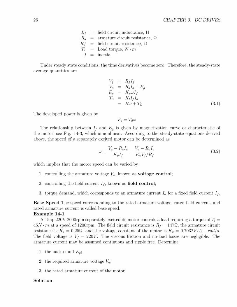
Lf = field circuit inductance, HRa = armature circuit resistance, ΩRf = field circuit resistance, ΩTL = Load torque, N · mJ = inertia
Under steady state conditions, the time derivatives become zero. Therefore, the steady-stateaverage quantities are
Vf = RfIf
Va = RaIa + Eg
Eg = KvωIf
Td = KtIfIa
= Bω + TL (3.1)
The developed power is given byPd = Tdω
The relationship between If and Eg is given by magnetization curve or characteristic ofthe motor, see Fig. 14-3, which is nonlinear. According to the steady-state equations derivedabove, the speed of a separately excited motor can be determined as
ω =Va − RaIa
KvIf=
Va − RaIa
KvVf/Rf(3.2)
which implies that the motor speed can be varied by
1. controlling the armature voltage Va, known as voltage control;
2. controlling the field current If , known as field control;
3. torque demand, which corresponds to an armature current Ia for a fixed field current If .
Base Speed The speed corresponding to the rated armature voltage, rated field current, andrated armature current is called base speed.Example 14-1
A 15hp 220V 2000rpm separately excited dc motor controls a load requiring a torque of Tl =45N ·m at a speed of 1200rpm. The field circuit resistance is Rf = 147Ω, the armature circuitresistance is Ra = 0.25Ω, and the voltage constant of the motor is Kv = 0.7032V/A − rad/s.The field voltage is Vf = 220V . The viscous friction and no-load losses are negligible. Thearmature current may be assumed continuous and ripple free. Determine
1. the back emmf Eg;
2. the required armature voltage Va;
3. the rated armature current of the motor.
Solution

3.2. OPERATING MODES 27
1.
ω =2πn
60=
2π(1200rpm)
60= 125.66rad/s
If =Vf
Rf=
220V
147Ω= 1.497
Eg = KvωIf = 0.7032 × 125.66 × 1.497 = 132.28V
2.
Ia =Td
KtIf
=45
0.7032 × 1.497= 42.75
Va = RaIa + Eg = 0.25 × 42.75 + 132.28 = 142.97V
3. Since 1hp is equal to 746W,
Irated =Prated
Vrated
=15 × 746
220= 50.87A
3.2 Operating Modes
In variable-speed applications, a dc motor may be operating in one or more modes: motoring,regenerative braking, dynamic braking, plugging, and four quadrants.
Motoring The arrangement for motoring is shown in Fig. 14-7a. In this mode,
Eg < Va
Ia > 0If > 0
The motor develops torque to meet the load demand.Regenerative braking The arrangement for regenerative braking is shown in Fig. 14-7b.
In this mode, the motor acts as a generator and develops an induced voltage Eg.
Eg > Va
Ia < 0If > 0
The kinetic energy of the motor is returned to the supply.Dynamic braking The arrangement for dynamic braking, as shown in Fig.14-7c, is similar
to that of regenerative braking, except the supply voltage Va is replaced by a braking resistanceRb. The kinetic energy of the motor is dissipated in Rb.
Plugging Plugging is a type of braking. Fig.14-7d shows the connection for plugging. Thearmature terminals are reversed while running. The supply voltage Va and Eg are in the samedirection. The armature current produces a braking torque. The field current is positive.
Four quadrants Fig. 14-8 shows the polarities of Va, Eg, and Ia for a separately exciteddc motor.
Quadrant I: forward motoring
Va > 0

28 CHAPTER 3. DC DRIVES
Eg > 0Va > Eg
Ia > 0ω > 0
Td > 0
Quadrant II: forward braking
Va > 0Eg > 0Va < Eg
Ia < 0ω > 0
Td < 0
Quadrant III: reverse motoring
Va < 0Eg < 0
−Va > −Eg
Ia < 0ω < 0
Td < 0
Note that the polarity of Eg can be reversed by changing the direction of field current or byreversing the armature terminals.
Quadrant IV: reverse braking
Va < 0Eg < 0
−Va < −Eg
Ia > 0ω < 0
Td > 0
3.3 Single-Phase Full-Wave Converter Drive
In order to control the speed of the motor, we need to adjust the armature supply voltage Va
or the field supply voltage Vf , which implies that we need variable dc voltage supplies. As weknow, controlled rectifiers provide a variable dc output voltage from a fixed as voltage, whereaschoppers can provide a variable dc voltage from a fixed dc voltage. According to variable dcsupplies, dc drives can be classified into three types:
1. Single-phase drives
(a) Single-phase half-wave converter drives (up to 0.5kW)

3.3. SINGLE-PHASE FULL-WAVE CONVERTER DRIVE 29
(b) Single-phase semi-converter drives (up to 15kW)
(c) Single-phase full-wave converter drives (up to 15kW)
(d) Single-phase dual converter drives (up to 15kW)
2. Three-phase drives
(a) Three-phase half-wave converter drives (up to 40kW)
(b) Three-phase semi-converter drives (up to 115kW)
(c) Three-phase full-wave converter drives (up to 1500kW)
(d) Three-phase dual converter drives (up to 1500kW)
3. Chopper drives
We shall consider only single-phase full-wave converter drive here due to time limitations.Fig. 14-13 shows a connection of single-phase full-converter drive. Both armature and field
circuits are supplied by single-phase full-wave converters. The armature converter provides+Va or −Va, and allows operation in the first and fourth quadrants. During reverse braking inquadrant IV, the back emf of the motor can be reversed by reversing the field excitation.
Recall that a single-phase full-wave converter provides an output voltage
Va =2Vm
πcos αa, 0 ≤ αa ≤ π
for the armature circuit, and
Vf =2Vm
πcos αf , 0 ≤ αf ≤ π
for the field circuit.Example 14-3 The speed of a separately excited dc motor is controlled by a one-phase full-wave converter in Fig. 14-13a. The field circuit is also controlled by a full converter and thefield current is set to the maximum possible value. The ac supply voltage to the armature andfield converters is one-phase, 440V, 60Hz. The armature resistance is Ra = 0.25Ω, the fieldcircuit resistance is Rf = 175Ω, and the motor voltage constant is Kv = 1.4V/A − rad/s. Thearmature current corresponding to the load demand is Ia = 45A. The viscous friction andno-load losses are negligible. The inductances of the armature and field circuits are sufficientto make the armature and field currents continuous and ripple-free. If the delay angle of thearmature converter is αa = 60() and the armature current is Ia = 45A, determine
1. the torque developed by the motor Td,
2. the speed ω,
3. the input power factor PF of the drive.
Solution: Vs = 440V, Vm =√
2 × 440 = 622.25V, Ra = 0.25Ω, Rf = 175Ω, αa = 60, andKv =1.4V/A − rad/s.

30 CHAPTER 3. DC DRIVES
1. The maximum field voltage(and current) would be obtained for a delay angle of αf = 0and
Vf =2Vm
π=
2 × 622.25
π= 396.14V
The field current is
If =Vf
Rf=
396.14
175= 2.26A
The developed torque is
Td = TL = KvIfIa = 1.4 × 2.26 × 45 = 142.4N · m
2. The armature voltage is
Va =2Vm
πcos 60 =
2 × 622.25
πcos 60 = 198.07V
The back emf is
Eq = Va − IaRa = 198.07 − 45 × 0.25 = 186.82V
The speed is
ω =Eq
KvIf=
186.82
1.4 × 2.26= 59.05rad/s or 564rpm
3. Assuming lossless converters, the total input power from the supply is
Pi = VaIa + VfIf = 198.07 × 45 + 396.14 × 2.26 = 9808.4W
The input current of the armature converter for a highly inductive load is shown in Fig.14-9b and its rms value is Isa = Ia = 45A. The rms value of the input current of fieldconverter is Isa = If = 2.26A. The effective rms supply current can be found from
Is = (I2sa + I2
sf)1/2
= (452 + 2.262)1/2 = 45.06A (3.3)
and the input volt-ampere rating, V I = VsIs = 440 × 45.06 = 19, 826.4. Neglecting theripples, the input power is approximately
PF =Pi
V I=
9808.4
19, 826.4= 0.495(lagging)
From Eq. (5-27),
PF =
(2√
2
π)
)cos αa =
(2√
2
π)
)cos 60 = 0.45(lagging)
ExampleA 220V, 3hp, 1800rpm seperately excited dc motor is controlled by a one-phase full-wave
converter with an ac source of 230V at 60Hz. Assume that full load efficiency of the motor is88% and enough field inductance is added to ensure continuous current for any torque greaterthan 25% of rated torque. Ra = 1.5Ω.
3.3. SINGLE-PHASE FULL-WAVE CONVERTER DRIVE 31
1. Determine the firing angle α to obtain rated torque at 1200rpm.
2. Compute the firing angle for the rated breaking torque at -1800rpm.
3. Find the firing angle corresponding to a torque of 35N ·m and speed of 480rpm, assumingcontinuous conduction.
Solution
1. Since η = Pout/Pin and Pin = VaIa, we have
Ia =Pin
Va=
Poutη
Va=
746(3hp)(0.88)
220V= 11.56A
It follows from Va = Ea + IaRa that the back emf at rated speed of 1800rpm is given by
(Ea)1800 = Va − IaRa = 220V − (11.56A)(1.5Ω) = 202.66V
Note that (Ea)1800 = Kvω1800If and (Ea)1200 = Kvω1200If . Then, we have
(Ea)1800
(Ea)1200
=ω1800
ω1200
As a result, the back emf at the speed of 1200rpm is
(Ea)1200 =ω1200
ω1800(Ea)1800 =
1200
1800202.66 = 135.11V
In order to obtain rated torque at 1200rpm, the armature voltage should be
Va = (Ea)1200 + IaRa = 135.11V + (11.56A)(1.5Ω) = 152.36V
which is the output voltage of the full-wave converter, that is,
Va =2Vm cos α
π=
2√
2Vs cos α
π
which implies that
cos α =Vaπ
2√
2Vs
=152.36π
2√
2(230V )= 0.736
So, the firing angle is α = 42.6.
2. Note that (Ea)−1800 = −202.66V , which means that the armature voltage for the ratedbraking torque at -1800rpm is
Va = (Ea)−1800 + IaRa = −202.66V + (11.56A)(1.5Ω) = −185.32
Then, we get
cos α =Vaπ
2√
2Vs
=−185.32π
2√
2(230V )= −0.8953
So, the firing angle is α = 153.5.

32 CHAPTER 3. DC DRIVES
3. The speed in radian per second for n = 1800rpm is
ω =2πn
60=
2π(1800)
60= 188.57rad/s
Note Ea = KvωIf . Then the motor voltage constant Kv satisfies
KvIf =Ea
ω=
202.66V
188.57rad/s= 1.075
The armature current corresponding to the torque of 35N · m is
Ia =Td
KvIf=
35N · m1.075
= 32.56A
The back emf is given by
(Ea)480 = KvIfω480 = 1.0752π(480rpm)
60= 54V
The armature voltage is calculated as
Va = (Ea)480 + IaRa = 54V + (32.56A)(1.5Ω) = 102.84V
Then, we get
cos α =Vaπ
2√
2Vs
=102.84π
2√
2(230V )= 0.4967
So, the firing angle is α = 60.2.
ExampleThe speed of a 125hp, 600V, 1800rpm, separately excited dc motor is controlled by a three-
phase full converter as shown below. The converter is operated from a three-phase, 480V,60Hz supply. The rated armature current of the motor is 164A. The motor parameters areRa = 0.0874Ω, La = 6.5mH, and KaΦ = 0.33V/rpm. The converter and ac supply areconsidered to be ideal.
1. Find no-load speeds at firing angles α = 0 and α = 30. Assume that, at no load, thearmature current is 10% of the rated current and is continuous.
2. Find the firing angle to obtain the rated speed of 1800rpm at rated motor current.
3. Compute the speed regulation for the firing angle obtained in part 2.
Solution
1. No-load condition. The armature current is
Ia = 10% = 16.5A

3.3. SINGLE-PHASE FULL-WAVE CONVERTER DRIVE 33
and the supply phase voltage is
Vp =480√
3= 277V
The motor terminal voltage is
Vt =3√
6 × 277
πcos α = 648 cosα
For α = 0, Vt = 648V , so the motor back emf is
Ea = Vt − IaRa = 648 − (16.5 × 0.0874) = 646.6V
and no-load speed is
n0 =Ea
KaΦ=
646.6
0.33= 1959rmp
For α = 30, Vt = 648 cos 30 = 561.2V , so the motor back emf is
Ea = Vt − IaRa = 561.2 − (16.5 × 0.0874) = 559.8V
and no-load speed is
n0 =Ea
KaΦ=
559.8
0.33= 1696rmp
2. Full-load condition. The motor back emf Ea at 1800rpm is
Ea = KaΦn = 0.33 × 1800 = 594V
The motor terminal voltage at rated current is
Vt = Ea + IaRa = 594 + (165 × 0.0874) = 608.4V
Therefore,
α = cos−1(
Vt
648
)= cos−1
(608.4
648
)= 20.1
3. Speed regulation. At full load the motor current is 165A and the speed is 1800rpm. Ifthe load is thrown off, keeping the firing angle the same at α = 20.1, the motor currentdecreases to 16.5A. Therefore
Ea = Vt − IaRa = 608.4 − (16.5 × 0.0874) = 606.96V
and the no-load speed is
n0 =Ea
KaΦ=
606.96
0.33= 1839.3rmp
The speed regulation is
SP =1839.3 − 1800
1800× 100% = 2.18%