Embed Size (px)
Citation preview

7/27/2019 Chap6-Introduction to Digital Electronics
http://slidepdf.com/reader/full/chap6-introduction-to-digital-electronics 1/81
Jaeger/Blalock 9/25/03
Microelectronic Circuit DesignMcGraw-Hill
Chap 6 - 1
Chapter 6
Introduction to Digital Electronics
Microelectronic Circuit Design
Richard C. Jaeger Travis N. Blalock
7/27/2019 Chap6-Introduction to Digital Electronics
http://slidepdf.com/reader/full/chap6-introduction-to-digital-electronics 2/81
Jaeger/Blalock 9/25/03
Microelectronic Circuit DesignMcGraw-Hill
Chap 6 - 2
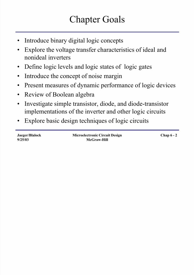
Chapter Goals
• Introduce binary digital logic concepts
• Explore the voltage transfer characteristics of ideal and
nonideal inverters
• Define logic levels and logic states of logic gates• Introduce the concept of noise margin
• Present measures of dynamic performance of logic devices
• Review of Boolean algebra
• Investigate simple transistor, diode, and diode-transistor
implementations of the inverter and other logic circuits
• Explore basic design techniques of logic circuits

7/27/2019 Chap6-Introduction to Digital Electronics
http://slidepdf.com/reader/full/chap6-introduction-to-digital-electronics 3/81
Jaeger/Blalock 9/25/03
Microelectronic Circuit DesignMcGraw-Hill
Chap 6 - 3
Brief History of Digital Electronics
• Digital electronics can be found in many applications inthe form of microprocessors, microcontrollers, PCs, DSPs,and an uncountable number of other systems.
• The design of digital circuits has progressed from resistor-
transistor logic (RTL) and diode-transistor logic (DTL) totransistor-transistor logic (TTL) and emitter-coupled logic(ECL) to complementary MOS (CMOS)
• The density and number of transistors in microprocessors
has increased from 2300 in the 1971 4-bit 4004microprocessor to 25 million in the more recent IA-64 chipand it is projected to reach over one billion transistors by2010

7/27/2019 Chap6-Introduction to Digital Electronics
http://slidepdf.com/reader/full/chap6-introduction-to-digital-electronics 4/81
Jaeger/Blalock 9/25/03
Microelectronic Circuit DesignMcGraw-Hill
Chap 6 - 4
Ideal Logic Gates
• Binary logic gates are the most common style of
digital logic
• The output will consist of either a 0 (low) or a 1 (high)
• The most basic digital building block is the inverter

7/27/2019 Chap6-Introduction to Digital Electronics
http://slidepdf.com/reader/full/chap6-introduction-to-digital-electronics 5/81
Jaeger/Blalock 9/25/03
Microelectronic Circuit DesignMcGraw-Hill
Chap 6 - 5
The Ideal Inverter
The ideal inverter has the following voltage transfer characteristic
(VTC) and is described by the following symbol
V+ and V- are the supply rails, and VH and VL describe
the high and low logic levels at the output

7/27/2019 Chap6-Introduction to Digital Electronics
http://slidepdf.com/reader/full/chap6-introduction-to-digital-electronics 6/81
Jaeger/Blalock 9/25/03
Microelectronic Circuit DesignMcGraw-Hill
Chap 6 - 6
Logic Level Definitions
An inverter operating with power supplies at V+ and0 V can be implemented using a switch with a
resistive load

7/27/2019 Chap6-Introduction to Digital Electronics
http://slidepdf.com/reader/full/chap6-introduction-to-digital-electronics 7/81
Jaeger/Blalock 9/25/03
Microelectronic Circuit DesignMcGraw-Hill
Chap 6 - 7
Logic Voltage Level Definitions
• VL – The nominal voltage corresponding to a low-logic
state at the input of a logic gate for vi = VH
• VH – The nominal voltage corresponding to a high-logic
state at the output of a logic gate for vi = VL
• VIL – The maximum input voltage that will be recognized
as a low input logic level
• VIH – The maximum input voltage that will be recognized
as a high input logic level
• VOH – The output voltage corresponding to an inputvoltage of VIL
• VOL – The output voltage corresponding to an input
voltage of VIH

7/27/2019 Chap6-Introduction to Digital Electronics
http://slidepdf.com/reader/full/chap6-introduction-to-digital-electronics 8/81
Jaeger/Blalock 9/25/03
Microelectronic Circuit DesignMcGraw-Hill
Chap 6 - 8
Logic Voltage Level Definitions (cont.)
Note that for the VTC of the nonideal inverter, there is now an
undefined logic state

7/27/2019 Chap6-Introduction to Digital Electronics
http://slidepdf.com/reader/full/chap6-introduction-to-digital-electronics 9/81
Jaeger/Blalock 9/25/03
Microelectronic Circuit DesignMcGraw-Hill
Chap 6 - 9
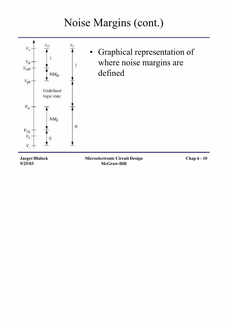
Noise Margins
• Noise margins represent “safety margins” that
prevent the circuit from producing erroneous
outputs in the presence of noisy inputs
• Noise margins are defined for low and high inputlevels using the following equations:
NML = VIL – VOL
NMH = VOH – VIH
7/27/2019 Chap6-Introduction to Digital Electronics
http://slidepdf.com/reader/full/chap6-introduction-to-digital-electronics 10/81
Jaeger/Blalock 9/25/03
Microelectronic Circuit DesignMcGraw-Hill
Chap 6 - 10
Noise Margins (cont.)
• Graphical representation of
where noise margins are
defined

7/27/2019 Chap6-Introduction to Digital Electronics
http://slidepdf.com/reader/full/chap6-introduction-to-digital-electronics 11/81
Jaeger/Blalock 9/25/03
Microelectronic Circuit DesignMcGraw-Hill
Chap 6 - 11
Logic Gate Design Goals
• An ideal logic gate is highly nonlinear that attempts toquantize the input signal to two discrete states, but in anactual gate, the designer should attempt to minimize theundefined input region while maximizing noise margins
• The input should produce a well-defined output, andchanges at the output should have no effect on the input
• Voltage levels of the output of one gate should becompatible with the input levels of a proceeding gate
• The gate should have sufficient fan-out and fan-incapabilities
• The gate should consume minimal power (and area for ICs) and still operate under the design specifications

7/27/2019 Chap6-Introduction to Digital Electronics
http://slidepdf.com/reader/full/chap6-introduction-to-digital-electronics 12/81
Jaeger/Blalock 9/25/03
Microelectronic Circuit DesignMcGraw-Hill
Chap 6 - 12
Dynamic Response of Logic Gates
• An important figure of merit to describe logic
gates is their response in the time domain
• The rise and fall times, tf and tr , are measured at
the 10% and 90% points on the transitions between the two states as shown by the following
expressions:
V10% = VL + 0.1ΔV
V90% = VL + 0.9ΔV = VH – 0.1ΔV

7/27/2019 Chap6-Introduction to Digital Electronics
http://slidepdf.com/reader/full/chap6-introduction-to-digital-electronics 13/81
Jaeger/Blalock 9/25/03
Microelectronic Circuit DesignMcGraw-Hill
Chap 6 - 13
Propagation Delay
• Propagation delay describes the amount of time between a
change at the 50% point input to cause a change at the 50%
point of the output described by the following:
• The high-to-low prop delay, τPHL, and the low-to-high prop
delay, τPLH, are usually not equal, but can be described asan average value:
2
PLHPHLP
2
LH50%
V V V

7/27/2019 Chap6-Introduction to Digital Electronics
http://slidepdf.com/reader/full/chap6-introduction-to-digital-electronics 14/81
Jaeger/Blalock 9/25/03
Microelectronic Circuit DesignMcGraw-Hill
Chap 6 - 14
Dynamic Response of Logic Gates

7/27/2019 Chap6-Introduction to Digital Electronics
http://slidepdf.com/reader/full/chap6-introduction-to-digital-electronics 15/81
Jaeger/Blalock 9/25/03
Microelectronic Circuit DesignMcGraw-Hill
Chap 6 - 15
Power Delay Product
• The power-delay product (PDP) is use as a metric
to describe the amount of energy required to
perform a basic logic operation and is given by the
following equation when P is the average power dissipated be the logic gate:
P P PDP

7/27/2019 Chap6-Introduction to Digital Electronics
http://slidepdf.com/reader/full/chap6-introduction-to-digital-electronics 16/81
Jaeger/Blalock 9/25/03
Microelectronic Circuit DesignMcGraw-Hill
Chap 6 - 16
Review of Boolean Algebra
A Z
0 1
1 0
A B Z
0 0 0
0 1 11 0 1
1 1 1
A B Z
0 0 0
0 1 01 0 0
1 1 1
NOT
Truth Table
OR Truth Table
ANDTruth Table
A B Z
0 0 1
0 1 01 0 0
1 1 0
A B Z
0 0 1
0 1 11 0 1
1 1 0
NOR Truth Table
NANDTruth Table

7/27/2019 Chap6-Introduction to Digital Electronics
http://slidepdf.com/reader/full/chap6-introduction-to-digital-electronics 17/81
Jaeger/Blalock 9/25/03
Microelectronic Circuit DesignMcGraw-Hill
Chap 6 - 17
Logic Gate Symbols and BooleanExpressions
7/27/2019 Chap6-Introduction to Digital Electronics
http://slidepdf.com/reader/full/chap6-introduction-to-digital-electronics 18/81
Jaeger/Blalock 9/25/03
Microelectronic Circuit DesignMcGraw-Hill
Chap 6 - 18
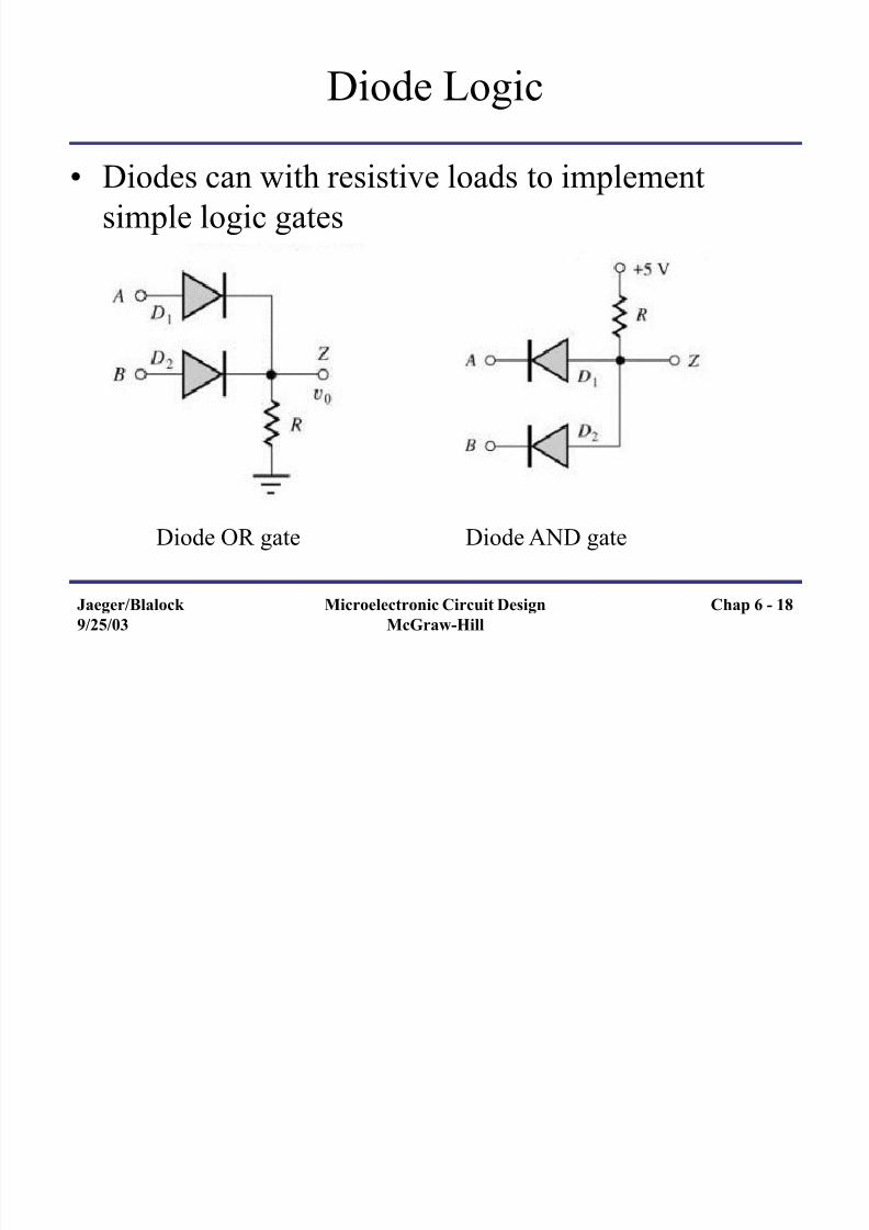
Diode Logic
• Diodes can with resistive loads to implement
simple logic gates
Diode OR gate Diode AND gate

7/27/2019 Chap6-Introduction to Digital Electronics
http://slidepdf.com/reader/full/chap6-introduction-to-digital-electronics 19/81
Jaeger/Blalock 9/25/03
Microelectronic Circuit DesignMcGraw-Hill
Chap 6 - 19
Diode Transistor Logic
• Since diode gates are limited to AND and OR functions, the diodes can be combined withtransistors to complete the basic logic functions
such as the following NAND gate

7/27/2019 Chap6-Introduction to Digital Electronics
http://slidepdf.com/reader/full/chap6-introduction-to-digital-electronics 20/81
Jaeger/Blalock 9/25/03
Microelectronic Circuit DesignMcGraw-Hill
Chap 6 - 20
NMOS Logic Design
• MOS transistors (both PMOS and NMOS) can be
combined with resistive loads to create single
channel logic gates
• The circuit designer is limited to altering circuit
topology and width-to-length, or W/L, ratio since
the other factors are dependent upon processing parameters
7/27/2019 Chap6-Introduction to Digital Electronics
http://slidepdf.com/reader/full/chap6-introduction-to-digital-electronics 21/81
Jaeger/Blalock 9/25/03
Microelectronic Circuit DesignMcGraw-Hill
Chap 6 - 21
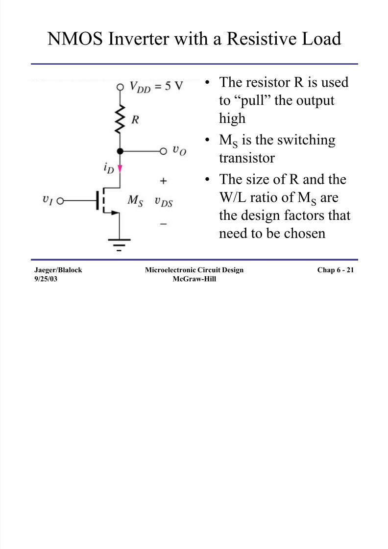
NMOS Inverter with a Resistive Load
• The resistor R is used
to “pull” the output
high
• MS is the switchingtransistor
• The size of R and the
W/L ratio of MS arethe design factors that
need to be chosen

7/27/2019 Chap6-Introduction to Digital Electronics
http://slidepdf.com/reader/full/chap6-introduction-to-digital-electronics 22/81
Jaeger/Blalock 9/25/03
Microelectronic Circuit DesignMcGraw-Hill
Chap 6 - 22
Load Line Visualization
• The following
illustrates the
operation of the
NMOS output (vDS)characteristics where
the following
equation describes
the load line
RiV v D DD DS

7/27/2019 Chap6-Introduction to Digital Electronics
http://slidepdf.com/reader/full/chap6-introduction-to-digital-electronics 23/81
Jaeger/Blalock 9/25/03
Microelectronic Circuit DesignMcGraw-Hill
Chap 6 - 23
NMOS with Resistive Load DesignExample
• Design a NMOS resistive load inverter for
– VDD = 3.3 V
– P = 0.1 mW when VL = 0.2 V
– K n = 60 μA/V2
– VTN = 0.75 V
• Find the value of the load resistor R and the W/Lratio of the switching transistor MS

7/27/2019 Chap6-Introduction to Digital Electronics
http://slidepdf.com/reader/full/chap6-introduction-to-digital-electronics 24/81
Jaeger/Blalock 9/25/03
Microelectronic Circuit DesignMcGraw-Hill
Chap 6 - 24
Example continued
• First the value of the current through the resistor
must be determined by using the following:
• The value of the resistor can now be found by the
following which assumes that the transistor is on
or the output is low:
AV
mW
V
P
I DD DD 3.303.3
1.0
k A
V V
I
V V R
DD
L DD 1023.30
2.03.3

7/27/2019 Chap6-Introduction to Digital Electronics
http://slidepdf.com/reader/full/chap6-introduction-to-digital-electronics 25/81
Jaeger/Blalock 9/25/03
Microelectronic Circuit DesignMcGraw-Hill
Chap 6 - 25
Example Continued
• For vI = VL = 0.2V, the transistor’s vGS will be less
than the threshold voltage, therefore it will be
operating in the triode region. Using the linear
equation for a MOSFET, the W/L ratio can befound:
1
1
1
03.1
2.022.075.03.310603.30
2
6
'
S
S
L L
TN H
S
n D
L
W
LW A
V V
V V L
W K I

7/27/2019 Chap6-Introduction to Digital Electronics
http://slidepdf.com/reader/full/chap6-introduction-to-digital-electronics 26/81
Jaeger/Blalock 9/25/03
Microelectronic Circuit DesignMcGraw-Hill
Chap 6 - 26
On-Resistance of MS
• The NMOS resistive load
inverter can be thought of
as a resistive divider
when the output is low,described by the
following expression:
R R RV V on
on DD L

7/27/2019 Chap6-Introduction to Digital Electronics
http://slidepdf.com/reader/full/chap6-introduction-to-digital-electronics 27/81
Jaeger/Blalock 9/25/03
Microelectronic Circuit DesignMcGraw-Hill
Chap 6 - 27
On-Resistance of MS (cont.)
2
1
' DS TN GS n
D
DS on
vV v
L
W K
i
v R
When the NMOS resistive load inverter’s output is
low, the On-Resistance of the NMOS can be
calculated with the following expression:
Note that R on should be kept small compared to R toensure that VL remains low, and also that its value is
nonlinear which has a dependence on vDS

7/27/2019 Chap6-Introduction to Digital Electronics
http://slidepdf.com/reader/full/chap6-introduction-to-digital-electronics 28/81
Jaeger/Blalock 9/25/03
Microelectronic Circuit DesignMcGraw-Hill
Chap 6 - 28
Noise Margin Analysis
• The following equations can be used to determine
the various parameters needed to determine the
noise margin of NMOS resistive load inverters
R K
V V
R K V
R K V V
R K V V
R K V V
n
DDOL
n
DD
n
TN IH
n
DDOH
n
TN IL
3
2
63.11
2
1
1
7/27/2019 Chap6-Introduction to Digital Electronics
http://slidepdf.com/reader/full/chap6-introduction-to-digital-electronics 29/81
Jaeger/Blalock 9/25/03
Microelectronic Circuit DesignMcGraw-Hill
Chap 6 - 29
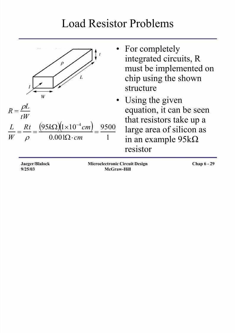
Load Resistor Problems
• For completelyintegrated circuits, R must be implemented onchip using the shownstructure
• Using the givenequation, it can be seen
that resistors take up alarge area of silicon asin an example 95k Ωresistor
1
9500
001.0
10195 4
cm
cmk Rt
W
L
tW
L R

7/27/2019 Chap6-Introduction to Digital Electronics
http://slidepdf.com/reader/full/chap6-introduction-to-digital-electronics 30/81
Jaeger/Blalock 9/25/03
Microelectronic Circuit DesignMcGraw-Hill
Chap 6 - 30
Using Transistors in Place of a Resistor
• NMOS load w/a) gate connected
to the source b) gate connected
to groundc) gate connected
to VDD
d) gate biased to
linear region
e) a depletionmode NMOS
Note that a) and b)are not useful

7/27/2019 Chap6-Introduction to Digital Electronics
http://slidepdf.com/reader/full/chap6-introduction-to-digital-electronics 31/81
Jaeger/Blalock 9/25/03 Microelectronic Circuit DesignMcGraw-Hill Chap 6 - 31
Static Design of the NMOS SaturatedLoad Inverter
Schematic for a NMOS
saturated load inverter
Cross-section for a NMOS
saturated load inverter

7/27/2019 Chap6-Introduction to Digital Electronics
http://slidepdf.com/reader/full/chap6-introduction-to-digital-electronics 32/81
Jaeger/Blalock 9/25/03 Microelectronic Circuit DesignMcGraw-Hill Chap 6 - 32
NMOS Saturated Load Inverter DesignStrategy
• Given VDD, VL, and the power level, find IDD from VDD and
power
• Assume MS off, and find high output voltage level VH
• Use the value of VH for the gate voltage of MS andcalculate (W/L)S of the switching transistor based on the
design values of IDD and VL
• Find (W/L)L (load transistor) based on IDD and VL
• Check the operating region assumptions of MS and ML for vo = VL
• Verify design with a SPICE simulations

7/27/2019 Chap6-Introduction to Digital Electronics
http://slidepdf.com/reader/full/chap6-introduction-to-digital-electronics 33/81
Jaeger/Blalock 9/25/03 Microelectronic Circuit DesignMcGraw-Hill Chap 6 - 33
NMOS Saturated Load Inverter DesignExample
• Design an saturated load inverter given the
following specifications:
A I
V V
V V
DD
L
DD
30
2.0
3.3
V
V
V V V
V A K
F
TOTN
n
6.02
5.0
75.0
/25 2'

7/27/2019 Chap6-Introduction to Digital Electronics
http://slidepdf.com/reader/full/chap6-introduction-to-digital-electronics 34/81
Jaeger/Blalock 9/25/03 Microelectronic Circuit DesignMcGraw-Hill Chap 6 - 34
NMOS Saturated Load Inverter DesignExample
• First find VH
V V V
V V
V V V V V V
H
H H
F F H TO DDTNL DD H
01.4,11.2
6.06.05.075.03.3
22

7/27/2019 Chap6-Introduction to Digital Electronics
http://slidepdf.com/reader/full/chap6-introduction-to-digital-electronics 35/81
Jaeger/Blalock 9/25/03 Microelectronic Circuit DesignMcGraw-Hill Chap 6 - 35
NMOS Saturated Load Inverter DesignExample
• For vo = VL,MS is
off (triode
region) and ML is
in saturation, findthe W/L ratios of
the two
transistors
19.2
1
81.02.03.3102530
81.06.06.02.05.075.0
1
76.4
2.02
2.075.011.2102530
2
26
2'
6
'
L
L
TNL
TNLGSL
L
n DL
S
S
L L
TN H
S
n DS
L
W
L
W A
V V
V V L
W K I
L
W
L
W A
V V
V V L
W K I

7/27/2019 Chap6-Introduction to Digital Electronics
http://slidepdf.com/reader/full/chap6-introduction-to-digital-electronics 36/81
Jaeger/Blalock 9/25/03 Microelectronic Circuit DesignMcGraw-Hill Chap 6 - 36
NMOS Saturated Load Inverter Design Noise Margin Analysis
• The basic noise margin equations are still the same as for
previous inverters, but there are different expressions for the
components
OL R
TNLOL DDOLTNS IH
L
S R
F F OLTOTNL
R
TNL DDOL
TNL DD H OH
TNS IL
V K
V V V V V V
LW LW K
V V V
K
V V V
V V V V
V V
22
)/()/(
22
31
The equations can be written as a
quadratic equation,but an iterative
process must be used to solve for VOL
and VTNL
1) Choose an initial VOL
2) Calculate the corresponding VTNL
3) Update VOL
4) Repeat 2 and 3 until the system
converges

7/27/2019 Chap6-Introduction to Digital Electronics
http://slidepdf.com/reader/full/chap6-introduction-to-digital-electronics 37/81
Jaeger/Blalock 9/25/03 Microelectronic Circuit DesignMcGraw-Hill Chap 6 - 37
NMOS Inverter with a Linear LoadDevice
• This alternative inverter has a load transistor that is biased with VGG
defined by thefollowing:
• This causes the loadtransistor to operate inthe linear region
TNL DDGG V V V

7/27/2019 Chap6-Introduction to Digital Electronics
http://slidepdf.com/reader/full/chap6-introduction-to-digital-electronics 38/81
Jaeger/Blalock 9/25/03 Microelectronic Circuit DesignMcGraw-Hill Chap 6 - 38
NMOS Inverter with a Depletion-modeLoad
• With the addition of a
depletion-mode NMOS
(VTH < 0V), it is possible
to configure an inverter as shown
• VGSL = 0 V for this
configuration meaning
that ML is always
operating in saturation

7/27/2019 Chap6-Introduction to Digital Electronics
http://slidepdf.com/reader/full/chap6-introduction-to-digital-electronics 39/81
Jaeger/Blalock 9/25/03 Microelectronic Circuit DesignMcGraw-Hill Chap 6 - 39
Design of a NMOS Inverter with aDepletion-mode Load
• To find (W/L)L given iDL:
• To find (W/L)S where VH = VDD use the same
technique as used for the resistor load inverter:
2'
2 TNL L
n
DL
V L
W K i
L L
TN H
S
n D V V
V V L
W K I
2
'
7/27/2019 Chap6-Introduction to Digital Electronics
http://slidepdf.com/reader/full/chap6-introduction-to-digital-electronics 40/81
Jaeger/Blalock 9/25/03 Microelectronic Circuit DesignMcGraw-Hill Chap 6 - 40
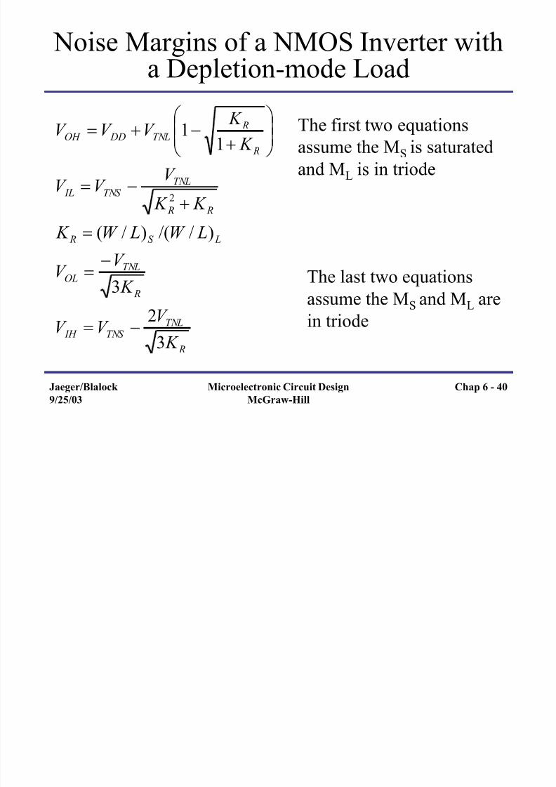
Noise Margins of a NMOS Inverter witha Depletion-mode Load
R
TNLTNS IH
R
TNLOL
LS R
R R
TNL
TNS IL
R
RTNL DDOH
K
V V V
K
V V
LW LW K
K K
V V V
K
K V V V
3
23
)//()/(
11
2
The first two equations
assume the MS is saturated
and ML is in triode
The last two equations
assume the MS and ML arein triode

7/27/2019 Chap6-Introduction to Digital Electronics
http://slidepdf.com/reader/full/chap6-introduction-to-digital-electronics 41/81
Jaeger/Blalock 9/25/03 Microelectronic Circuit DesignMcGraw-Hill Chap 6 - 41
NMOS Inverter Summary
• Resistive load inverter takes up too much area for and IC
design
• The saturated load configuration is the simplest design, but
VH
never reaches VDD
and has a slow switching speed
• The linear load inverter fixes the speed and logic level
issues, but it requires an additional power supply for the
load gate
• The depletion-mode NMOS load requires the most
processing steps, but needs the smallest area to achieve the
highest speed, VH = VDD, and best combination of noise
margins

7/27/2019 Chap6-Introduction to Digital Electronics
http://slidepdf.com/reader/full/chap6-introduction-to-digital-electronics 42/81
Jaeger/Blalock 9/25/03 Microelectronic Circuit DesignMcGraw-Hill Chap 6 - 42
Typical Inverter Characteristic
Inverter w/
Resistor
Load
Saturated
Load
Inverter
Linear
Load
Inverter
Inverter w/
Depletion-
Mode Load
VH 5.0 V 3.4 V 5.0 V 5.0 V
VL 0.25 V 0.25 V 0.25 V 0.25 V
NML 0.34 V 0.32 V 0.02 V 0.69 V
NMH 1.43 V 0.69 V 2.78 V 2.25 VArea (μm2) 9500 6.92 9.36 4.21
7/27/2019 Chap6-Introduction to Digital Electronics
http://slidepdf.com/reader/full/chap6-introduction-to-digital-electronics 43/81
Jaeger/Blalock 9/25/03 Microelectronic Circuit DesignMcGraw-Hill Chap 6 - 43
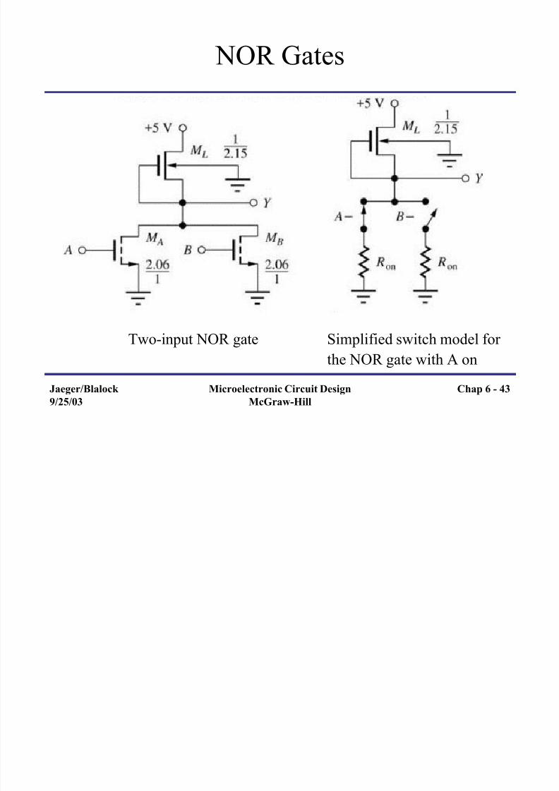
NOR Gates
Simplified switch model for
the NOR gate with A on
Two-input NOR gate

7/27/2019 Chap6-Introduction to Digital Electronics
http://slidepdf.com/reader/full/chap6-introduction-to-digital-electronics 44/81
Jaeger/Blalock
9/25/03
Microelectronic Circuit Design
McGraw-Hill
Chap 6 - 44
NAND Gates
Simplified switch model
for the NOR gate with Aand B on (right)
Two-input NAND gate
(left)

7/27/2019 Chap6-Introduction to Digital Electronics
http://slidepdf.com/reader/full/chap6-introduction-to-digital-electronics 45/81
Jaeger/Blalock
9/25/03
Microelectronic Circuit Design
McGraw-Hill
Chap 6 - 45
NAND Gate Device Size Selection
• The NAND switching transistors can be sized based on the
depletion-mode load inverter
• To keep the low voltage level to be comparable to the
inverter, the desired R ON of MA and MB must be 0.5R ON of MS,Inverter
• This can be accomplished by approximately doubling the
(W/L)A and (W/L)B
• The sizes can also be chosen by using the design value of VL and using the following equation:
DS TN GS
S
n DS DS TN GS
S
n D vV v L
W K vvV v
L
W K i
'' 5.0

7/27/2019 Chap6-Introduction to Digital Electronics
http://slidepdf.com/reader/full/chap6-introduction-to-digital-electronics 46/81
Jaeger/Blalock
9/25/03
Microelectronic Circuit Design
McGraw-Hill
Chap 6 - 46
NAND Gate Device Size Selection(continued)
• Two sources of error that arise are the facts that
VSB and VGS of the two transistors do not equal.
These factors should be considered for proper gate
design
• The technique used to calculate the size of the load
transistor for the depletion-mode load inverter is
the exact same as for this NAND gate

7/27/2019 Chap6-Introduction to Digital Electronics
http://slidepdf.com/reader/full/chap6-introduction-to-digital-electronics 47/81
Jaeger/Blalock
9/25/03
Microelectronic Circuit Design
McGraw-Hill
Chap 6 - 47
Layout of the NMOS Depletion-Mode NOR and NAND Gates

7/27/2019 Chap6-Introduction to Digital Electronics
http://slidepdf.com/reader/full/chap6-introduction-to-digital-electronics 48/81
Jaeger/Blalock
9/25/03
Microelectronic Circuit Design
McGraw-Hill
Chap 6 - 48
Complex NMOS Logic Design
An advantage of NMOS technology is that it is simple to design
complex logic functions based on the NOR and NAND gates
The circuit in thefigure has the logic
function:
Y = A + BC + BD

7/27/2019 Chap6-Introduction to Digital Electronics
http://slidepdf.com/reader/full/chap6-introduction-to-digital-electronics 49/81
Jaeger/Blalock
9/25/03
Microelectronic Circuit Design
McGraw-Hill
Chap 6 - 49
Complex Logic Gate Transistor Sizing
• There are two ways to find the W/L ratios of the
switching transistors
1) Using the worst case (longest) path and choosing theW/L ratio such that the R ON of the multiple legs match
similar to the technique used to find the W/L ratios in
the NAND Gate
2) Partitioning the circuit into series sub-networks, and
make the equivalent on-resistances equal

7/27/2019 Chap6-Introduction to Digital Electronics
http://slidepdf.com/reader/full/chap6-introduction-to-digital-electronics 50/81
Jaeger/Blalock
9/25/03
Microelectronic Circuit Design
McGraw-Hill
Chap 6 - 50
Complex Logic Gate Transistor Sizing
The figure on the leftshows the worst casetechnique to find thesizes where(W/L)S=2.06 is thereference inverter ratiofor this technology andthe longest path is 3transistors are in series
The figure on the rightshows the partitioning
technique to find thesizes which gives two4.12/1 ratios in serieswhich is 2(2.06/1)

7/27/2019 Chap6-Introduction to Digital Electronics
http://slidepdf.com/reader/full/chap6-introduction-to-digital-electronics 51/81
Jaeger/Blalock
9/25/03
Microelectronic Circuit Design
McGraw-Hill
Chap 6 - 51
Static Power Dissipation
• Static Power Dissipation is the average power
dissipation of a logic gate when the output is in both
the high and low states
• IDDH = current in the circuit for vO = VH
• IDDL = current in the circuit for vO = VL
• Since IDDH = 0 A for vO = VH:
2 DDL DD DDH DD
av I V I V P
2
DDL DDav
I V P
7/27/2019 Chap6-Introduction to Digital Electronics
http://slidepdf.com/reader/full/chap6-introduction-to-digital-electronics 52/81
Jaeger/Blalock
9/25/03
Microelectronic Circuit Design
McGraw-Hill
Chap 6 - 52
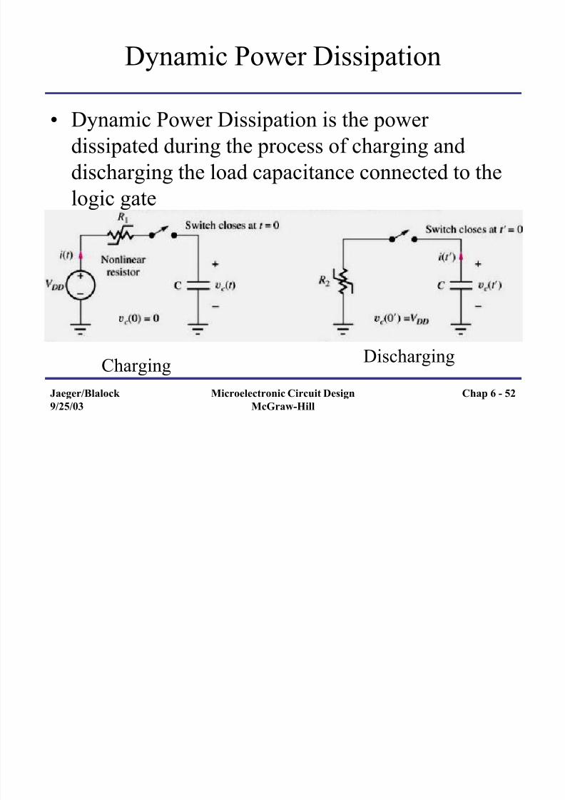
Dynamic Power Dissipation
• Dynamic Power Dissipation is the power
dissipated during the process of charging and
discharging the load capacitance connected to the
logic gate
DischargingCharging

7/27/2019 Chap6-Introduction to Digital Electronics
http://slidepdf.com/reader/full/chap6-introduction-to-digital-electronics 53/81
Jaeger/Blalock
9/25/03
Microelectronic Circuit Design
McGraw-Hill
Chap 6 - 53
Dynamic Power Dissipation
• Based on the energy equation, the energy delivered to
the capacitor can be found by:
• The energy stored by the capacitor is:
• The energy lost in the resistive elements is given by:
2
)(
)0(0
)()( DD
V
V
C DD DD D CV dvt iV C dt t iV E C
C
2
2
DD D
CV E
2
2
DDS D L
CV E E E

7/27/2019 Chap6-Introduction to Digital Electronics
http://slidepdf.com/reader/full/chap6-introduction-to-digital-electronics 54/81
Jaeger/Blalock
9/25/03
Microelectronic Circuit Design
McGraw-Hill
Chap 6 - 54
Dynamic Power Dissipation
• The total energy lost in the first charging and
discharging of the capacitor through resistive elements
is given by:
• Thus it can be seen that for every cycle (frequency)
that the gate is changed, the dynamic power
dissipation is given by:
2
22
22DD
DD DDTD CV CV CV E
f CV P DD D
2
7/27/2019 Chap6-Introduction to Digital Electronics
http://slidepdf.com/reader/full/chap6-introduction-to-digital-electronics 55/81
Jaeger/Blalock
9/25/03
Microelectronic Circuit Design
McGraw-Hill
Chap 6 - 55
Power Scaling in MOS Logic
• By reducing the W/L of the load and switching
transistors of an inverter, it is possible to reduce
the power dissipation by the same factor without
sacrificing VH and VL. This same concept worksfor increasing the power which will increase the
dynamic response.

7/27/2019 Chap6-Introduction to Digital Electronics
http://slidepdf.com/reader/full/chap6-introduction-to-digital-electronics 56/81
Jaeger/Blalock
9/25/03
Microelectronic Circuit Design
McGraw-Hill
Chap 6 - 56
Power Scaling in MOS Logic
a) Original Saturated Load Inverter
b) Saturated Load inverter designed to operate at 1/3 the power
c) Original Depletion-Mode Inverter
d) Depletion-mode inverter designed to operate at twice the power
7/27/2019 Chap6-Introduction to Digital Electronics
http://slidepdf.com/reader/full/chap6-introduction-to-digital-electronics 57/81
Jaeger/Blalock
9/25/03
Microelectronic Circuit Design
McGraw-Hill
Chap 6 - 57
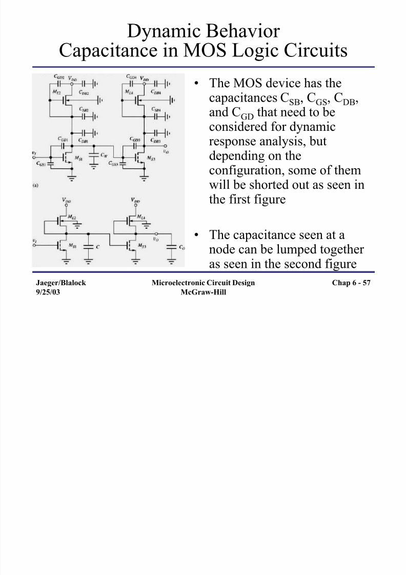
Dynamic Behavior Capacitance in MOS Logic Circuits
• The MOS device has thecapacitances CSB, CGS, CDB,and CGD that need to beconsidered for dynamic
response analysis, butdepending on theconfiguration, some of themwill be shorted out as seen inthe first figure
• The capacitance seen at anode can be lumped together as seen in the second figure

7/27/2019 Chap6-Introduction to Digital Electronics
http://slidepdf.com/reader/full/chap6-introduction-to-digital-electronics 58/81
Jaeger/Blalock
9/25/03
Microelectronic Circuit Design
McGraw-Hill
Chap 6 - 58
Fan-out Limitations
• Static design constraints are not usually important
for MOS logic circuits since they normally drive
capacitive loads (i.e. the gate of a MOS)
• As the number of gates the output (fan-out) of alogic device has to drive, the load capacitance
increases, and the time response decreases
• This notion implies that the fan-out that a logic
circuit can drive will be limited to time delay
tolerances of the circuit

7/27/2019 Chap6-Introduction to Digital Electronics
http://slidepdf.com/reader/full/chap6-introduction-to-digital-electronics 59/81
Jaeger/Blalock
9/25/03
Microelectronic Circuit Design
McGraw-Hill
Chap 6 - 59
Dynamic Response of the NMOSInverter with a Resistive Load
• The rise and fall times and propagation delays are
given by the relationships:
where R and C are the resistance and capacitance
seen at the output
RC
RC t t
PHL PLH
f r
69.0
2.2

7/27/2019 Chap6-Introduction to Digital Electronics
http://slidepdf.com/reader/full/chap6-introduction-to-digital-electronics 60/81
Jaeger/Blalock
9/25/03
Microelectronic Circuit Design
McGraw-Hill
Chap 6 - 60
Dynamic Response of the NMOSInverter with a Resistive Load
• There are four
important times
that need to be
considered whencharacterizing the
dynamic response
of a logic circuit
which are denotet1 – t4 in the figure

7/27/2019 Chap6-Introduction to Digital Electronics
http://slidepdf.com/reader/full/chap6-introduction-to-digital-electronics 61/81
Jaeger/Blalock
9/25/03
Microelectronic Circuit Design
McGraw-Hill
Chap 6 - 61
Dynamic Response of the NMOSInverter with a Resistive Load
• It is also possible to calculate τPHL and tf by a
piecewise analysis technique, and are given by the
following equations:
TNS H
TNS
H
TNS H onS f
TNS H
TNS
L H
TNS H onS PHL
V V
V V
V V
V V V C Rt t t
V V
V
V V
V V C Rt t t t
1.022
9.0
9.02ln
214ln)(
14
2233

7/27/2019 Chap6-Introduction to Digital Electronics
http://slidepdf.com/reader/full/chap6-introduction-to-digital-electronics 62/81
Jaeger/Blalock
9/25/03
Microelectronic Circuit Design
McGraw-Hill
Chap 6 - 62
NMOS Inverter with a Depletion-ModeLoad Dynamic Response
• Just as in the resistive
load inverter, the
depletion-mode load
inverter has the same
dynamic responsecharacteristics that need
to be considered, and
has four times that
needed for calculations

7/27/2019 Chap6-Introduction to Digital Electronics
http://slidepdf.com/reader/full/chap6-introduction-to-digital-electronics 63/81
Jaeger/Blalock
9/25/03
Microelectronic Circuit Design
McGraw-Hill
Chap 6 - 63
NMOS Inverter with a Depletion-ModeLoad Dynamic Response
• The following are the basic equations for calculating
dynamic response characteristics
TNL
LTNL H TNLonLr
TNS H
TNS
H
TNS H
onS f
TNL
LTNL H
L H
TNLonL PLH
TNS H
TNS
L H
TNS H onS PHL
V
V V V V
V
V C Rt t t
V V
V V
V V
V V V
C Rt
V
V V V
V V
V C Rt t t
V V
V
V V
V V C Rt t t t
1.021
20ln
1.02
29.0
9.02
ln
214ln
214ln)(
14
223
2233
i h l i d

7/27/2019 Chap6-Introduction to Digital Electronics
http://slidepdf.com/reader/full/chap6-introduction-to-digital-electronics 64/81
Jaeger/Blalock
9/25/03
Microelectronic Circuit Design
McGraw-Hill
Chap 6 - 64
NMOS Inverter with a Depletion-ModeLoad Dynamic Response Example
• Find tf , tr , τPHL, τPLH and τ p for a depletion-mode
load inverter where:
– (W/L)S = 2.06/1 and (W/L)L = 1/2.15
– CLOAD = 0.1 pF – VTNS = 1 V and VTNL = -3 V
– VDD = 5 V and VL = 0.25 V
– K S = (2.06)(25 10-6 A/V2)
– K L = (25 10-6 A/V2)/2.15
– Neglect body effect
OS i h l i d

7/27/2019 Chap6-Introduction to Digital Electronics
http://slidepdf.com/reader/full/chap6-introduction-to-digital-electronics 65/81
Jaeger/Blalock
9/25/03
Microelectronic Circuit Design
McGraw-Hill
Chap 6 - 65
NMOS Inverter with a Depletion-ModeLoad Dynamic Response Example
• First find the on-resistances of the two NMOS
k
V
AV K R
k
V
AV V K R
TNL L
onL
TNS H S
onS
7.28
3
15.2
25
11
85.4
152506.2
11
2
2
NMOS I i h D l i M d

7/27/2019 Chap6-Introduction to Digital Electronics
http://slidepdf.com/reader/full/chap6-introduction-to-digital-electronics 66/81
Jaeger/Blalock
9/25/03
Microelectronic Circuit Design
McGraw-Hill
Chap 6 - 66
NMOS Inverter with a Depletion-ModeLoad Dynamic Response Example
• It is now possible to calculate the propagation
delays
ns
ns pF k
V
V V V
V V
V C R
ns pF k
V V
V
V V
V V C R
PHL PLH p
PLH
TNL
LTNL H
L H
TNLonL PLH
PHL
TNS H
TNS
L H
TNS H onS PHL
58.22
56.4)59.1)(1.0)(7.28(
214ln
590.0)22.1)(1.0)(85.4(
214ln
NMOS I i h D l i M d

7/27/2019 Chap6-Introduction to Digital Electronics
http://slidepdf.com/reader/full/chap6-introduction-to-digital-electronics 67/81
Jaeger/Blalock
9/25/03
Microelectronic Circuit Design
McGraw-Hill
Chap 6 - 67
NMOS Inverter with a Depletion-ModeLoad Dynamic Response Example
ns pF k t
V
V V V V
V
V C Rt
ns pF k t
V V
V V
V V
V V V C Rt
r
TNL
LTNL H TNL
onLr
f
TNS H
TNS
H
TNS H onS f
47.9)03.3)(1.0)(7.28(
1.021
20ln
25.1)57.2)(1.0)(85.4(
1.022
9.0
9.02ln
The rise and fall times can be calculated in the following
manner
NMOS I i h S d L d

7/27/2019 Chap6-Introduction to Digital Electronics
http://slidepdf.com/reader/full/chap6-introduction-to-digital-electronics 68/81
Jaeger/Blalock
9/25/03
Microelectronic Circuit Design
McGraw-Hill
Chap 6 - 68
NMOS Inverter with a Saturated LoadDynamic Response
• The following are the basic equations for calculating
dynamic response characteristics and can be used in a
similar manner as the previous example
C Rt
V V
V V
V V
V V V C Rt
C R
V V
V
V V
V V C R
onLr
TNS H
TNS
H
TNS H onS f
onL PLH
TNS H
TNS
L H
TNS H onS PHL
9
160
1.022
9.0
9.02ln
2
214ln

7/27/2019 Chap6-Introduction to Digital Electronics
http://slidepdf.com/reader/full/chap6-introduction-to-digital-electronics 69/81
Jaeger/Blalock
9/25/03
Microelectronic Circuit Design
McGraw-Hill
Chap 6 - 69
Comparison of Load Devices
• The current has
been normalized
to 50 μ Afor
vo
=VOL
=0.25V
isthefigurefor
thevarious
typesof
inverters

7/27/2019 Chap6-Introduction to Digital Electronics
http://slidepdf.com/reader/full/chap6-introduction-to-digital-electronics 70/81
Jaeger/Blalock
9/25/03
Microelectronic Circuit Design
McGraw-Hill
Chap 6 - 70
Comparison of Load Devices
• Body effect degrades the performance of the loaddevice
• The saturated load devices have the poorest τPLH since they have the lowest load current delivery
• The saturated load devices also reach zero current before the output reaches 5 V
• The linear load device is faster than the saturated
load device, but still slower than the resistive loadinverter.
• The fastest τPLH is from the depletion-mode device

7/27/2019 Chap6-Introduction to Digital Electronics
http://slidepdf.com/reader/full/chap6-introduction-to-digital-electronics 71/81
Jaeger/Blalock
9/25/03
Microelectronic Circuit Design
McGraw-Hill
Chap 6 - 71
Comparison of Load Devices
Simulated fall times for a
0.1 pF load
Simulated rise times for
a 0.1 pF load
7/27/2019 Chap6-Introduction to Digital Electronics
http://slidepdf.com/reader/full/chap6-introduction-to-digital-electronics 72/81
Jaeger/Blalock
9/25/03
Microelectronic Circuit Design
McGraw-Hill
Chap 6 - 72
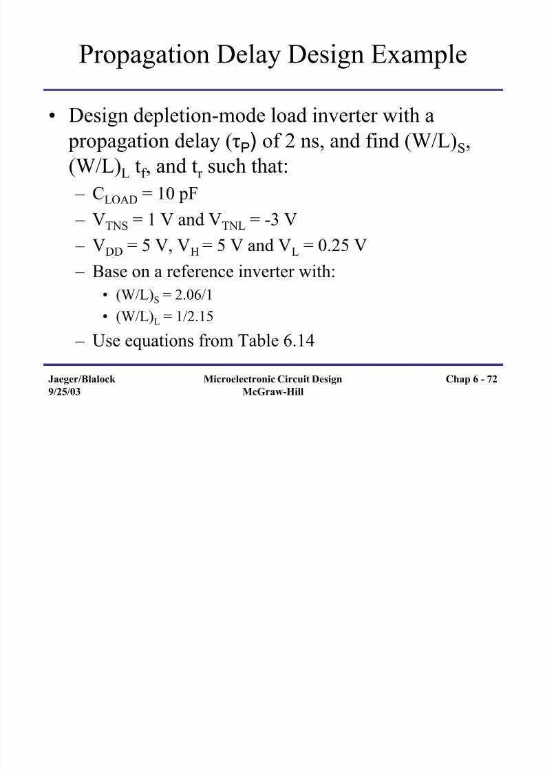
Propagation Delay Design Example
• Design depletion-mode load inverter with a
propagation delay (τP) of 2 ns, and find (W/L)S,
(W/L)L tf , and tr such that:
– CLOAD = 10 pF – VTNS = 1 V and VTNL = -3 V
– VDD = 5 V, VH = 5 V and VL = 0.25 V
– Base on a reference inverter with:
• (W/L)S = 2.06/1
• (W/L)L = 1/2.15
– Use equations from Table 6.14
7/27/2019 Chap6-Introduction to Digital Electronics
http://slidepdf.com/reader/full/chap6-introduction-to-digital-electronics 73/81
Jaeger/Blalock
9/25/03
Microelectronic Circuit Design
McGraw-Hill
Chap 6 - 73
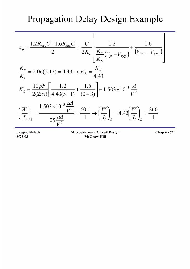
Propagation Delay Design Example
1
26643.4
1
1.60
25
10503.1
10503.1)30(
6.1
)15(43.4
2.1
)2(2
10
43.443.4)15.2(06.2
6.12.1
22
6.12.1
2
2
3
2
3
LS L
L
S L
L
S
TNLGSLTNS H
L
S L
onLonS p
L
W
L
W
V
AV A
L
W
V
A
ns
pF K
K K K K
V V V V
K
K K
C C RC R

7/27/2019 Chap6-Introduction to Digital Electronics
http://slidepdf.com/reader/full/chap6-introduction-to-digital-electronics 74/81
Jaeger/Blalock
9/25/03
Microelectronic Circuit Design
McGraw-Hill
Chap 6 - 74
Propagation Delay Design Example
ns
V V K L
W
C t
ns
V V K
L
W
C t
TNS H S
S
f
TNLGSL L
L
r
977.06.2
32.73.3

7/27/2019 Chap6-Introduction to Digital Electronics
http://slidepdf.com/reader/full/chap6-introduction-to-digital-electronics 75/81
Jaeger/Blalock
9/25/03
Microelectronic Circuit Design
McGraw-Hill
Chap 6 - 75
Propagation Delay Design Example
• Repeat the example, but use Table 6.16 to include
body effect
• First a scaling factor is needed to match this
design problems specifications
1551.0
10
2
1.3
1
2
2
1
pF
pF
ns
ns
C
C
P
P

7/27/2019 Chap6-Introduction to Digital Electronics
http://slidepdf.com/reader/full/chap6-introduction-to-digital-electronics 76/81
Jaeger/Blalock
9/25/03
Microelectronic Circuit Design
McGraw-Hill
Chap 6 - 76
Propagation Delay Design Example
nsns
nsns
t
t t t
nsns
nsns
t
t t t
L
W
L
W
L
W
L
W
P
P f f
P
P r r
L L
S S
97.01.3
25.1
4.81.3
213
1
1.72
15.2
1
155
1
319
1
06.2155
1
212
1
212
12
12

7/27/2019 Chap6-Introduction to Digital Electronics
http://slidepdf.com/reader/full/chap6-introduction-to-digital-electronics 77/81
Jaeger/Blalock
9/25/03
Microelectronic Circuit Design
McGraw-Hill
Chap 6 - 77
PMOS Logic
• PMOS logic circuits predated NMOS logic circuit, but
were replaced since they are usually operate at slower
speeds (note the change in the power supplies)
Resistive Load Saturated Load Linear Load Depletion-mode Load

7/27/2019 Chap6-Introduction to Digital Electronics
http://slidepdf.com/reader/full/chap6-introduction-to-digital-electronics 78/81
Jaeger/Blalock
9/25/03
Microelectronic Circuit Design
McGraw-Hill
Chap 6 - 78
PMOS NAND and NOR Gates
NOR Gate NAND Gate

7/27/2019 Chap6-Introduction to Digital Electronics
http://slidepdf.com/reader/full/chap6-introduction-to-digital-electronics 79/81

7/27/2019 Chap6-Introduction to Digital Electronics
http://slidepdf.com/reader/full/chap6-introduction-to-digital-electronics 80/81
Jaeger/Blalock
9/25/03
Microelectronic Circuit Design
McGraw-Hill
Chap 6 - 80
Silicon Art Examples

7/27/2019 Chap6-Introduction to Digital Electronics
http://slidepdf.com/reader/full/chap6-introduction-to-digital-electronics 81/81
End of Chapter 6