Embed Size (px)
Citation preview
CHAP,TER . ,' .., . t"' : "..
··ME,·D,I,UM SCALE INTEGRATION
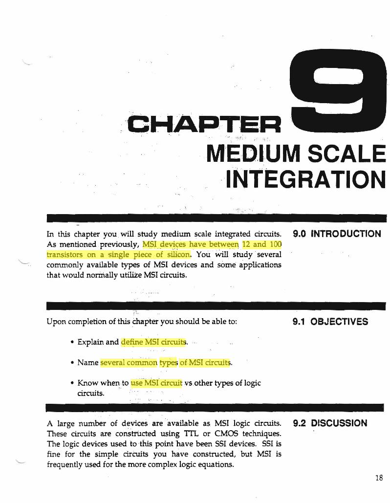
In this chapter you .will study medium scale integrated circuits. 9.0 INTRODUCTION As mentioned previously, MSJ.,~e~~es havebetwee~ 12 and 100 transistors on a ' single piece . of sruc-on. You Wmstudy several commonly available types of MSI devices and some appUcations that would normally utiliZeMSI circuits.
Upon completion of this chapter you should be able to: 9.1 OBJECTIVES
• Explain and def!ne MSI circuits.
• Name several common types oiMSI circuits.
• Know when,to useMSI circuit vsother types of logic circuits. '. , ..
A large number ·of devices ·are .available as MSI logic circuits. 9.2 DISCUSSION These circuits are constfuctedusing TIL or CMOS techniques. The logic devices used tothls point 'have been SS! devices. SS! is fine for the simple circuits you have constructed, but MSI is frequently used for the more complex logic equations.
18
. , ,
I ,, ' , _ ,
• ' ... 0 • .' , : .(, ,':t \ ' , I., ' . '~ ; .
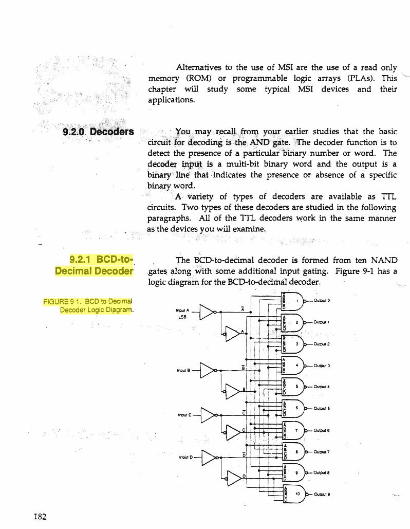
9.2.1 BCD-toDecimal Decoder
FIGURE 9-1. BCD to Decimal Decoder Logic DiSlgram.
Alternatives to the use of MSI are the use of a read only memory (ROM) or programmable logic arrays (PLAs). This 'chapter will study some typical MSI devices and their applications.
" . . . ¥OlJ"maYI:'~aJJ from your ~arlier studies that the basic "circtikior ~ecodirtg is ·,t11~ ANn 'gate. "-;'['he decoder function is to detect the presence of a particular 'b'mary number or word. The decoder ~!, is a multi-bit binary word and the output is a hmary :line that ,indicates the presence or absence of a specific binary wqrd.
, ~. . A, variety of types of decoders are available as TIL circuits. Two types of these decoders are studied in the following paragraphs. All of the TTL decoders work in the same manner as the .devicesyou will examine.
. .. ; ~ f . • 'c " . .... • .
, .. .
The BCD-to-decimal decoder is formed from ten NAND gates along ,With some 'addltlortal input gating. Figure '9-l has a logiC diagram for the BCD-to-decimcil decoder.
I"put A
LSB
Input B
InPut C
182
The MSlcomponent that implements the BCD-todecimal decode function is the 7442. This device is also known as a four ..t6-ten line d~pder. Select one of the possible output states and convince yourself that the output will only be true for a specific set of input drCUJl'\Stances.
Notice that ,1}ot all of , the possible input states are decoded: Decoding aU ' ,!i\P1Jt combinaq.oIlS would result in erroneous decoder out;putshotild a rtWIll:>er which is not between zero and nine appear on the input.
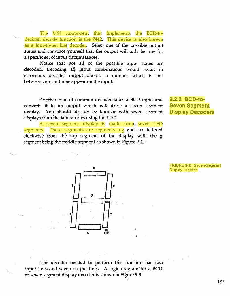
Another type of common decoder takeS a BCD input and converts it to an output which will drive a seven segment display. You shol.l1d 'aITeady be fanliliarwith seven segment displays from the laborat()ries using the LD-2.
A seven segment display is made from seven LED segments. These segments are segments a-g and are lettered clockwise from the top segment of the display with the g segment being the middle segment as shown in Figure 9-2. '
a I I
b
g
e c
"I r' "-----.;.I" •d DP
The decoder needed to perform this function has fOUI
input lines and seven output lines. A logic diagram fora BCDto-seven segment-display decoder is ~hown in Figure" 9-3.
9.2.2 BCD-toSeven Segment Display Decoders
FIGURE 9-2. Seven-Segment Display Labeling.
183
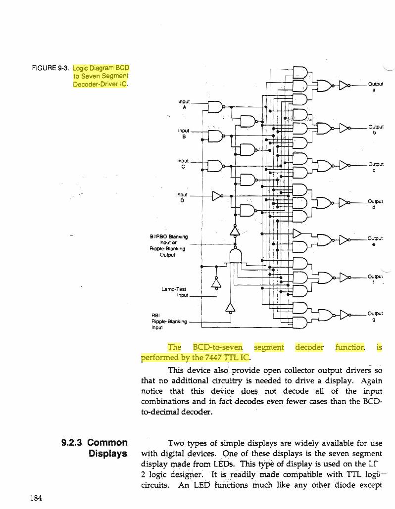
FIGURE 9-3. Logic Diagram BCD to Seven Segment Decoder-Driver IC. ;0--- OutPUt
a
Input _-.J-.....
A ~~----~ ~-+-+1-'1~
;»-__...,.... OutputInpUt_........;--'" bB .~H----~~
tm:m:1
~___ Output
Input ---+---l )c~t+----H...j-O..++-~ o .;:10--- Output
d
BIIRBO Blanki~ :»-__ Output Input or e
Ripple-Blanking Output
~__Output
I
Lamp·Test Input _.....--__
.»-_ OutputRBI Ripple-Blanking --t--_....J g Input L..-..--'-________-lo-.../
The BCD-to-seven segment decoder function is performed by the 74471TL IC.
, - This device also' provide open collector output drivers so
that no additional ciiCliitry is needed to drive a display. Again notice that this device ~o~ not. decode all of the input combinations and in fattdecodes even fewer cases than the BCDto-decimal decoder.
9.2.3 Common Two types of simple displays are widely available for use Displays with digjtal devices~ ,One of these displays is the seven segment
display made from LEOS. This type. of display is used on the Lr 2 logic desi~er. ' It is, readily' made compatible with TIL IOgll circuits. An 'LED functions much like any other diode except
184
c
that when it ,'conductsswficient current, the device will emit light. The two 'methods of driving an LED with a gate output are to:
1. Connect the gate output to ' the anode of the LED and the cathode of the 'LED to ground through a resistor. The LED will light 'wheri the gate output is HI. This is ,known as current sourcing operation. This"type of . operation is not the ,p;referred
: melliodofbiasing an LED to emit tight when using TIL qevices.
2. Connect the gate' otitput to the :cathode of the ' LED and , the anode of the LED to Vcc through a resistor. In this cOriliguration;the ::LEO will light when the gate output 'is LO. This is the current sinking mode of operation. Current sinking operation is preferred since most ITL ' gates can sink more current than they can source. Note that when a 'gate is-used to drive a LED that the current requirements of the LED are so high that no other 1TL device can ' be driven from the output of the gate driving the LED.
The different ways oLdriving LEOs have,resulted in two similar configurations of seven segment displays. The Common anode devices are made to be driven : by current sinking lOgic. The Common cathode ",C!cuit is ~<?r use , with, current sourcing lOgic. LED displays can be driven from, Jatchesor , can be multiplexed so that one decoder I driver can supply the needs of several digits of a display. When LEP displays are multiplexed, drive current is' modulated to the displays , which ' can result in brightness problems-if the drive puls~ are too short.
The second _ type of display which is frequently encountered is the Liquid Crystal Display , or LCD. This type of display is made from ' crystals ," which will change their light transmittance properties in the preSence of an electric field. This means that the ' LCO\ requires a'light source to be 'visible. Most LCOs receive enough room light to give good readability. Those that do not get ' enoug~ room ,light for "good readability often h~ve a backlight , Which provideS good ' readability in reduced ambient lighting. ' ,
The LCD works by changing the light's polarization. The LCD is constructed from two pieces of glass which sandwich the
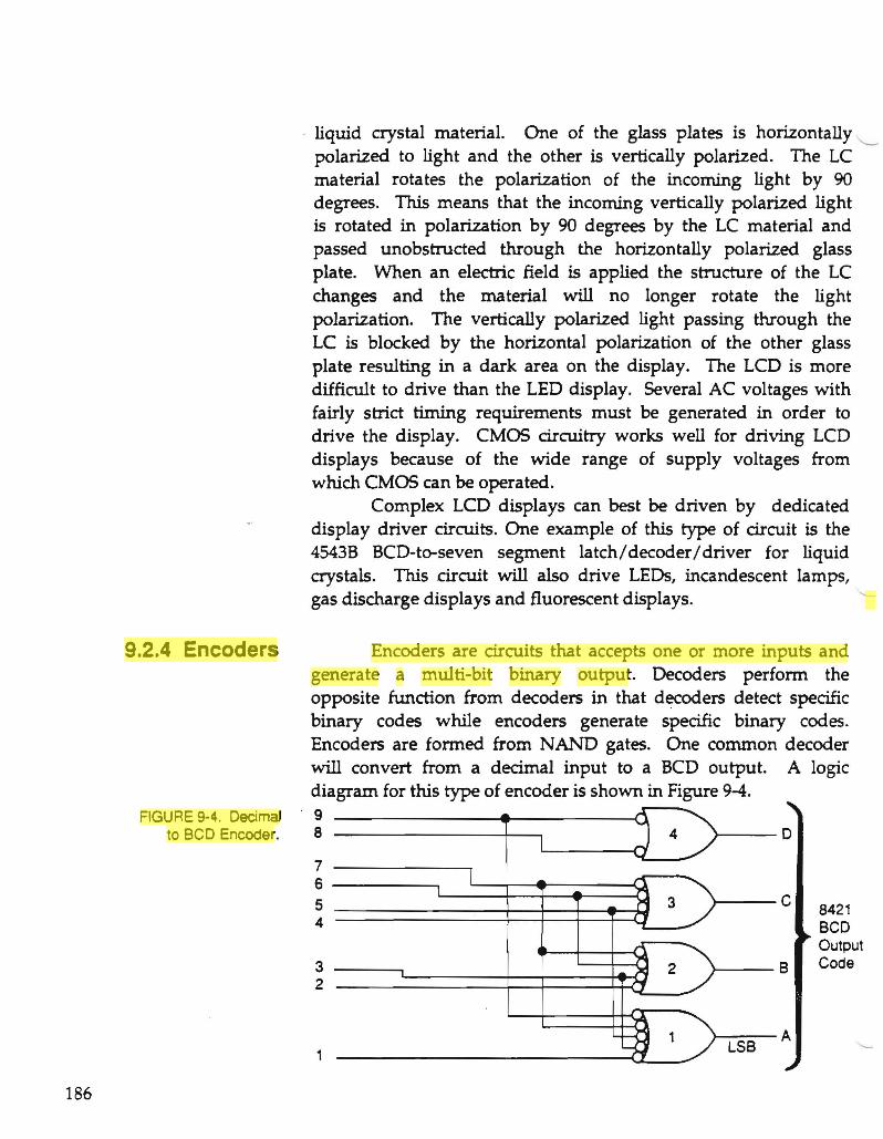
9.2.4 Encoders
FIGURE 9-4. Decimal to BCD Encoder.
liquid crystal material. One of the glass plates is horizontally ,--polarized to light and the other is vertically polarized. The LC material rotates the polarization of the incoming light by 90 degrees. This means that the incoming vertically polarized light is rotated in polarization by 90 degrees by the LC material and passed unobstructed through the hOrizontally polarized glass plate. When an electric field is applied the structure of the LC changes and the material will no longer rotate the light polarization. The vertically polarized light passing through the LC is blocked by the horizontal polarization of the other glass plate resulting in a dark area on the display. The LCD is more difficult to drive than the LED display. Several AC voltages with fairly strict timing requirements must be generated in order to drive the display. CMOS circuitry works well for driving LCD displays because of the wide range of supply voltages from which CMOS can be operated.
Complex LCD displays can best be driven by dedicated display driver circuits. One example of this type of circuit is the 4543B BCD-to-seven segment latch/decoder/driver for liquid crystals. This circuit will also drive LEOs, incandescent lamps, gas discharge displays and fluorescent displays. '
Encoders are circuits that accepts one or more inputs and generate a multi-bit binary output. Decoders perform the opposite function from decoders in that decoders detect specific binary codes while encoders generate specific binary codes. Encoders are formed from NAND gates. One common decoder will convert from a decimal input to a BCD output. A logic diagram for this type of encoder is shown in Figure 9-4. 9 8 j 4
I ..,.. 7"- 3
r1
~ 2 ..t1
:r ~ 1~~
0
7 6
C5 8421 4 BCD
Output Code3 B
2
A LSB1
186
This type of encoder would be used to convert from a decimal keypad like a ten-key.to,a B<;D output.
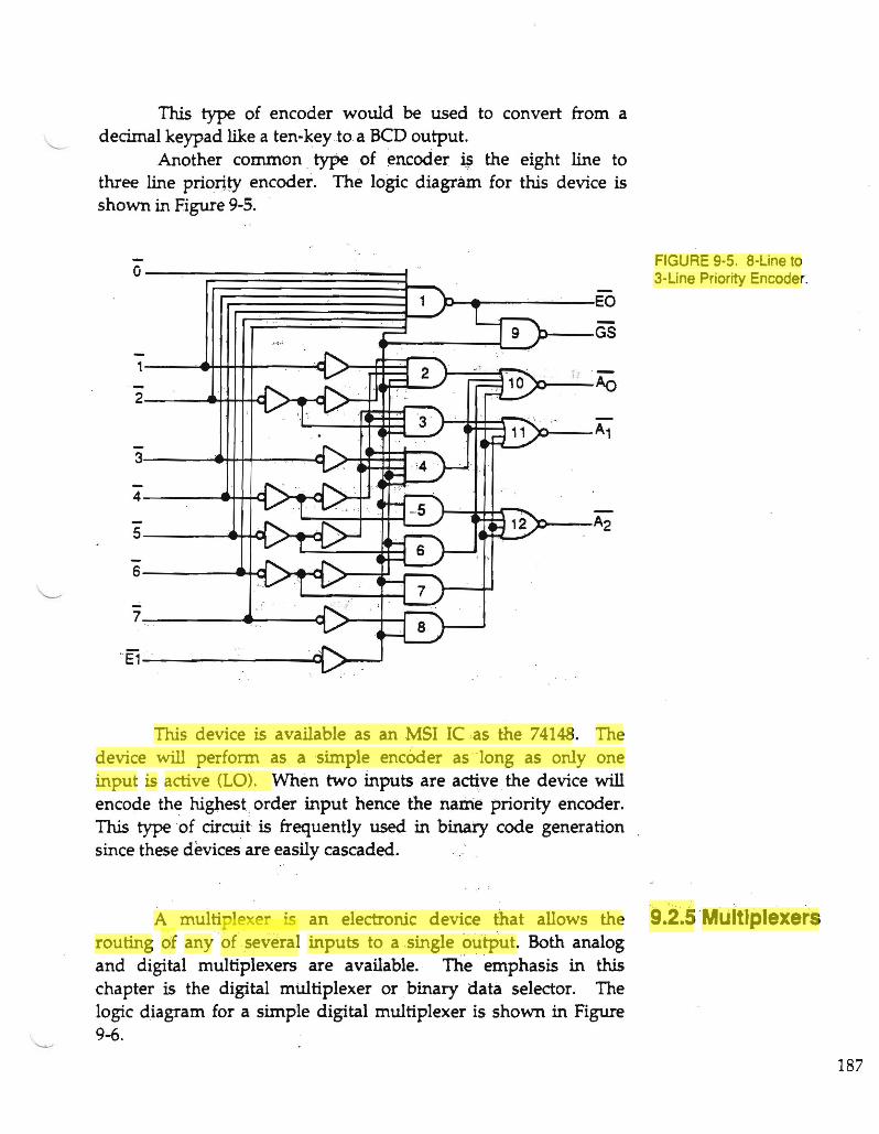
Another common , type of en(:oder i,? the eight line to three line prioIit.Y encoder. The logic diagram for this device is shown in Figure 9-5.
'2-_____~+++.g
-3------~~~~--Q
4---__t++-Q
-S----"4~.Q
-6------+<l
-7________~~----~
' E1-' '-----------....q ~---'
This device is available as anMSI IC ,as the 74148. The device will perform as a simple encOder as "long as only one input is active (LO). When two inputs are active the device will encode the highest order input hence the name priority encoder. This type of circuit is frequently used in binary code generation since these devices are easily cascaded..
A multiplexer is an electronic device that allows the routing df any ofseveral inputs to a single output. Both analog and digital multiplexers are available. The emphasis in this chapter is the digital multiplexer or binary data selector. The logic diagram for a simple digital multiplexer is shown in Figure 9-6.
FIGURE 9-5. a-Line to 3-Line Priority Encoder.
9.2.5 Multiplexers
187
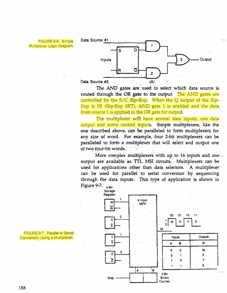
FIGURE 9-6, Simple Multiplexer Logic Diagram,
FIGURE 9-7. Parallel to Serial Conversion, Using a Multiplexer.
Data Source .!#~1__~_~_-r--~
0.-____,' S
>--OutputInputs
R 2
Data Source #2 (A) "
The AND gates are ' used to select which data source is routed through the 0:R gate to the output. The AND gates are controlled by· the SIC flip-:flop. ,When the Q output of the flipflop is HI (flip-flop SET), 'A,NDgClte lis enabled and the data from source 1 is ~~pplied to the ORgate for output.
The multiplexer .~ have several data inputs, one data output and soine contrOrihputs. Simple multiplexers, like the one described above/~rt be , paralleled to fonn multiplexers for any size of ,word. For eXam,ple, four 2-bit multiplexers can be paralleled. to form a multi,plexer that will select and output one of two four-bit words. " ._.. ': '
More complex mulfiplex~rS - With up to 16 inputs and one' output are available as TIL MSI circuits. Multiplexers can be
, used for applications other than data selectors. A ' multiplexer can be used for , parallel to , serial conversion by sequencing through the data inputs. This type of application is shown in
Figure 9-7. 4.Bit
Storage Register
2 Bit Step ---4 Binary
I.-.._......._~ Counter
o
4 Input MPX
00 01 10 11
1 rvilx r7l t01" L.J ' L~
Inputs
A B M
o 0 W
01 X
o V
Z
188
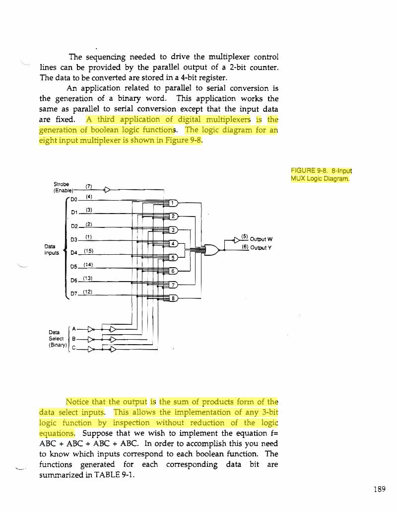
The sequencing needed to drive the multiplexer control lines can be provided by the parallel output of a 2-bit counter. The data to be converted are stored in a 4-bit register.
An application related to parallel to serial conversion is the generation of a binary word. This application works the same as parallel to serial conversion except that the input data are fixed. A third application of digital multiplexers is the generation of boolean logic functions. The logic diagram for an eight input multiplexer is shown in Figure 9-8.
Strobe (7) J"...(Enable)
D0
D1
D2
D3
D4
D5
(4)
(3)
(2)
(1 )
(15)
(14)
D6 . (13)
D7 (12)
!AB C
.----{)
I---{)
.....
I I
r..... .,..... .r-.. ..... J'.. ....
1-~
3r-.
4 ~ --2... rfL./
...§)--
7r---B
Output W r:-;,Data (6) Output Y Inputs
DataSelect (Binary)
Notice that the output is the sum of products form of the data select inputs. This allows the implementation of any 3-bit logic function by inspection without reduction of the logic equations. Suppose that we wish to implement the equation f= .ABC + ABC + ABC + ABC. In order to accomplish this you need to know which inputs correspond to each boolean function. The functions generated for each corresponding data bit are summarized in TABLE 9-1.
FIGURE 9-S. S-Input MUX Logic Diagram.
189
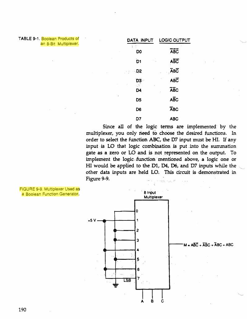
TABLE 9-1. Boolean Products of an 8-Bit Multiplexer.
FIGURE 9-9. Multiplexer Used as a Boolean Function Generator.
DATA INPUT LOGIC OUTPUT
DO ABC
01 ABC
' ,Q2 ,ABC
03 ' ABC ""
Dot -:. ABC
05 ABC
D6 ABC
07 ABC
Since all of the logic terms are implemented" by the multiplexer, you only need to choose the desired functions. In order to select the function ABC, ' the 07 input must be HI. H any input "is LO that logic comb~tionis put -into the summation gate as a zero or LO and is not _represented on the output. To implement the logkiunction " mentioned above, a logi~ one or HI would be applied to the .01, ·04, D6,and 07 inputs while the '-other data inputs are held LO. This circuit is demonstrated in Figure 9-9. "
"" a -Input . Multiplexer
...5 V
0
'II 1
2
3
4
" , , . " , .s ;
" 6 '.
. . , ":,: . "
7LSB ~~-
I I ,
M. ABE ... ABC ... ABC ... ABC
ABC
190
Other more, complex boolean functions can be generated by using input" va~bles instead ' of fixed input levels. For example, a four-bit truth table can 'be implemented utilizing an eight input m~,tiph~xer by using the 0 (fourth) data bit and it's complement as data inputs.
This type of circUit ' is ~oWh as a , folded data selector circuit. This type of circuit is desirable since implementing a four-bit truth 'table 'with fixed logic would require a sixteen input multiplexer which is a much more complex and costly circuit.
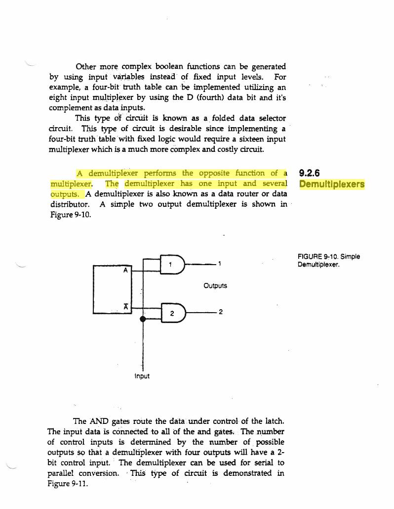
A demultiplexer performs the opposite function of a multiplexer. Th~ demultiplexer has one input and several outputs. A demultiplexer is also known as a data router or data distributor. A simple two output demultiplexer is shown in Figure 9-10.
A
X
~ 1
Outputs
2 2
Input
The AND gates route the data',under control of the latch. The input data is connected to all of the and gates; " The number of control inputs is determined by the number of " possible outputs so that a demultiplexer with four outputs will have a 2bit control inpht. • The demultiplexer can be used for serial to parallel conversion. . ThiS type of circuit is demonstrated in Figure 9-11.
'
9.2.6 Demultiplexers
'
FIGURE ~'O. Simple Demultiplexer.
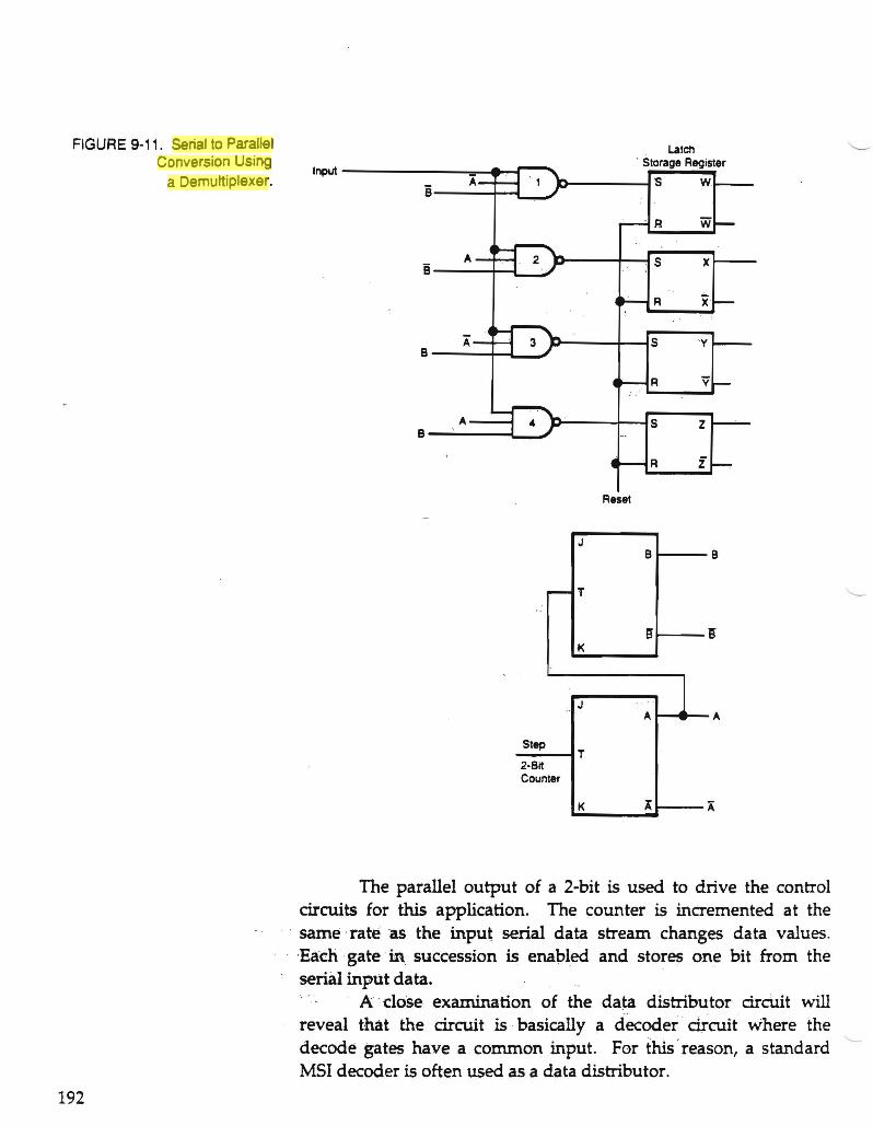
FIGURE 9-11. Serial to Parallel Latch Conversion Using . Siorage Register
Input a Demultiplexer. A s
B .
- R
A . SB
R
X
A----i B-----4-~
Reset
A S Y B
z
i
J B B
TI""""""
•...
~ K
J A
Step
2·Bit Counter
T
K A
A
The parallel output of a 2-bit is used to drive the control circuits for this application. The counter is incremented at the
. same 'rate -as the input serial data stream changes data values. . ·Each ·gate 'in succession is enabled and stores one bit from the
serial input data. . A dose examination of the data diStributor circuit will
reveal that the circuit is ·basically a decoder ' ctTcuit where the decode gates have a common input. For this "reason, a standard MSI decoder is often used as a data distributor.
192
The multiplexer and demultiplexers just discussed often receive their inputs from or deliver their outputs to some sort of
'- register. In bussed systems where the potential ·.for input from multiple data sources exists, 3-state registers provide a convenient method of providing these inputs and outputs.
3-state registers are available in any and all of the common register formats (PIPO, SISO, PISO, SIPO) and are available in packages with four, eight and sixteen bit widths. These registers operate in the same manner as the registers that you are familiar with except that they also have the capability of providing a high impedance output state.
9.2.7 3-State Registers
In this chapter you have studied MSI circuits. You learned what 9.3 SUMMARY MSI circuits are and some of their applications. You have studied decoders and their applications of detecting specific data and driving displays. You also learned about encoders and some of their applications.
Multiplexers and their applications . as data selectors, parallel to serial converters, and boolean equation generators were discussed. You studied demultiplexers and some typical applications of these devices and how some demultiplexers can be implemented with decoders. The final topic covered was the use of 3-state logic in conjunction with the circuits studied in this chapter.
1. Define a MSI circuit. 9.4 REVIEW QUESTIONS
193
2. What alternatives are available for the implementation of logic citcuits?
3. What is the basic decoder circuit?
4. Name the basic encoder circuit.
... ::·· t, 'I.'
5. Define a digital multiplexer.
6. . Describe a digital demultiplexer.
7. Give two applications of decoders.
194
8. What are three applications of multiplexers?
9. Name an application of demultiplexers.
10. How many control lines are needed for a 16 input multiplexer?
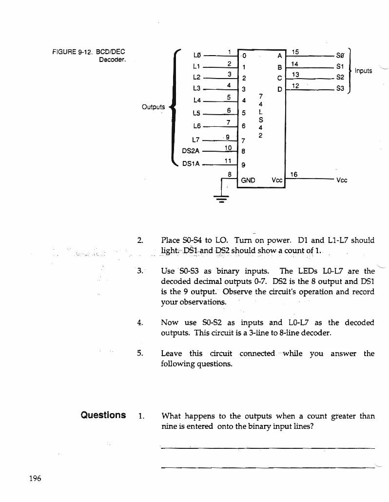
,---. In this lab exercise you will begin your study of MSLcircuits. In this 'lab exercise you Will also study the 4-line to ID-line decoder. This circuit is often used as a BCD to decimal decoder. It can also be used as a decoder for any number of binary .inputs less than four such as 3-line to 8-line decoders and 2-line to 4-line decoders.
LAB EXERCISE 9.1 Decoders
Objectives
LD-2 Logic Designer Materials
74LS42 4-Line to 10-Line Decoder
Jumper Wires
TIL Data Book
1. Wire DS1 DE and DS2 DE to 5 VOC. Now wire the circuit Procedure shown in Figure 9-12. This is the circuit for a BCD/DEC decoder.
195
1L0 2L1 3L2 4L3 5L4
6LS 7L6
9 · L7 10DS2A
11DS1A
r-L ,
- .....
0 A
1 B
2 C
3
4
5
6
7
7 4 L S 4 2
D
8
9
GND Vee
15 S9' 14 S1
Inputs13 S2 12 S3
16 Vee
FIGURE 9-12. BCDIOEC Decoder.
Outputs
2. Place 50-54 to LO. Turn on power. 01 and LI-L7 should light.i" DSlandQS2 should showa cOunt of 1. . . . ~- :. -. . ._. . ' '. . .. __, . .' .1. . ... ..;.. . . .. ," . '. . ' . ' . ,
·3. Use 50-53 as binary inputs. The LEOs LO-L7are the - decoded decimal outputs ~7. 052 is the 8 output and OSl is the 9 output. .. Observe the circuit's operation and record yoUr observations.
4. Now use SO-52 as inputs and LO-L7 as the decoded outputs. This circuit is a 3-line to B-line decoder.
5. Leave this circuit connected while you answer the following questions.
Questions 1. What happens to the outputs when a count greater than nine is entered onto the binary input lines?
196
2. What type of circuit could you use to tell that an invalid input had been entered on the 50-53 inputs?
3. What type of circult would you need to use to detect invalid inputs f()r the 3·iine to 8·linedecoder?
4. Are the outputs of the 74LS42 LO true or HI true?
5. The LD·2 itas ~. in~ernal display driver so that the outputs of the 74LS42 are driVing a ITL ' load 'and not a directly connected LED. Can the 74LS42 be used to drive an LED indicator directly? Explain your anSwer. '
In this lab exercise you will investigate the use oithe 7447 BCD· T~5EVEN·SEGMENT DECODERS/DRIVERS. You will also learn about the use of seven-segment displays. You will study implementing simple displays.
LAB EXERCISE 9.2 Decoder/Drivers
Objectives
LD-2 Logic Designer
7447 BCD-T0-7·Segment Decoders/Drivers
TIL 312 Common·Anode 7·Segment Display
Materials
Jumper Wires
197