Embed Size (px)
Citation preview

1
Shingo Tamaru
Spintronics Research Center (SRC)
National Institute of Advanced Industrial Science and Technology (AIST)
Seminar at AGH University of Science and Technology
May. 10th, 2016
Challenges in using spin torque oscillator
(STO) for practical microwave applications

2
Outline
1. Brief introduction of AIST and SRC
2. Challenges in using STOs for practical
microwave applications
1. STO based Phase locked loop (STO-PLL)
2. Ultrahigh sensitivity FMR (I-FMR)
3. Spatially resolved FMR (SRFMR)
3. Summary
Outline
3
1. Brief introduction of AIST and SRC
Brief introduction of AIST
4
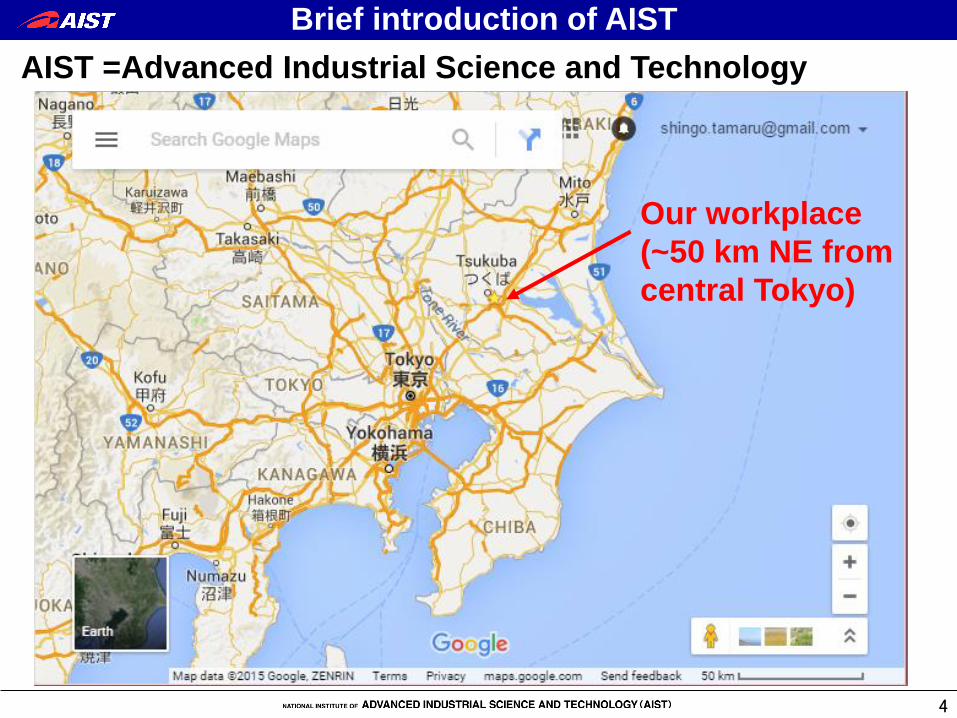
AIST =Advanced Industrial Science and Technology
Brief introduction of AIST
Our workplace
(~50 km NE from
central Tokyo)

5
Organization of Spintronics Research Center (SRC)
Brief introduction of AIST
Director: Shinji Yuasa
Deputy director: Akio Fukusima
Metal
Spintronics team
Semiconductor
Spintronics team
Theory
team
STT team
Leader: Hitoshi Kubota
Elec. field effect team
I belong to
this team.
Outside collaborators
• Osaka Univ.
• Tohoku Univ.
• CNRS Thales (France)
• Toshiba Corp.
• Tokyo Electron Corp.
• Denso Corp.
• Many other…..

6
Member photo of Spintronics Research Center
Brief introduction of AIST
Yuasa-san
Fukushima-san
Kubota-san
Me
Anna-san

7
AIST’s mission statement
Brief introduction of AIST
Greeting from President of AIST
(Mr. Chubachi)
AIST has been pursuing research
under the slogan of bringing
“technology to society” ….
US Department of Commerce, “ The advanced technology program: Reform with a purse” (2002.2)
Valley
of deathFindings in
basic
research
Technologies
useful for
society
AIST is here!
8
2. Challenges in using STOs for practical
microwave applications
1. STO based phase locked loop (STO-PLL)
Challenges in STOs

Rader
Google soli
9
Challenges in STOs
STO’s potential
applications
Consumer wireless
communications
Satellite
communications
Data storage
MAMR STO reader(Zhu, 2008) (Sato, 2012)
Microwave imaging
These apps require
highly stable yet
flexible microwave
source!

10
Challenges in STOs
The main topic of this presentation
• Wireless communication is the most demanding
microwave application in terms of oscillator
performance!
– Why? Because users have insatiable appetite for data
bandwidth.
– Phase noise is the dominant cause of spectrum
broadening.
– Narrower spectrum (equivalently, lower phase noise)
gives wider data bandwidth.
Let’s think about what needs to be done to use
STOs in wireless communication systems.
11
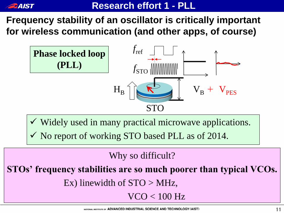
Widely used in many practical microwave applications.
No report of working STO based PLL as of 2014.
Frequency stability of an oscillator is critically important
for wireless communication (and other apps, of course)
Voltage Controlled Oscillator (VCO)
fVCO
VPES
frefPhase locked loop
(PLL)
Why so difficult?
STOs’ frequency stabilities are so much poorer than typical VCOs.
Ex) linewidth of STO > MHz,
VCO < 100 Hz
HB VB
STO
fSTO
VPES+
fref
Research effort 1 - PLL

12
Why STO based PLL?
Ref. in
10-100 MHz
Phase
Frequency
Detector
Voltage
Controlled
Oscillator
1/N
Down counter
Microwave
frequencyVar. in
•Current PLLs use either LC tank or dielectric
resonator based oscillator as a VCO.
•LC tank and dielectric resonators are quite large
(.1 ~ 1 mm).
•STO is much smaller than such VCOs, leading
to significant size and cost reduction!
Phase Error Signal
(VPES)
VCTR
in
RF
out
Loop
Filter
Block diagram of standard PLL
C.-W. Hsu et al., CICC, Sep. 2011
Research effort 1 - PLL
13
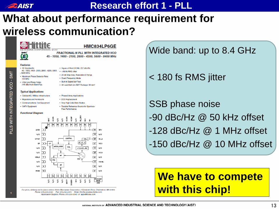
What about performance requirement for
wireless communication?
Research effort 1 - PLL
Wide band: up to 8.4 GHz
< 180 fs RMS jitter
SSB phase noise
-90 dBc/Hz @ 50 kHz offset
-128 dBc/Hz @ 1 MHz offset
-150 dBc/Hz @ 10 MHz offset
We have to compete
with this chip!

14
Structure of STO used in this work
MgO(1)FeB(2)
MgO(1)
CoFeB(3)Ru(0.85)
CoFe(2.5)PtMn(15)
Ta(5)
Mfree
Mref
d=400 nm
H. Kubota et. al, APEX 6, 103003 (2013)
VB (mV)
STO having a perpendicularly magnetized free layer, (PMF-STO)
Research effort 1 - PLL

15
-60
-50
-40
-30
-20
-10
0
7.244 7.294 7.344 7.394 7.444
Spectrum of free running PMF-STO
output under different VB
114.9
120.2125.6
128.2130.9
136.2
141.5
VB
(mV)
Frequency (GHz)
Pow
er (
dB
m)
7.31
7.32
7.33
7.34
7.35
7.36
7.37
113 118 123 128 133 138 143
Pea
k f
req.
(G
Hz)
VB (mV)
𝑑𝑓
𝑑𝑉𝐵= −2.1
Agility
MHz/mV
Research effort 1 - PLL
16
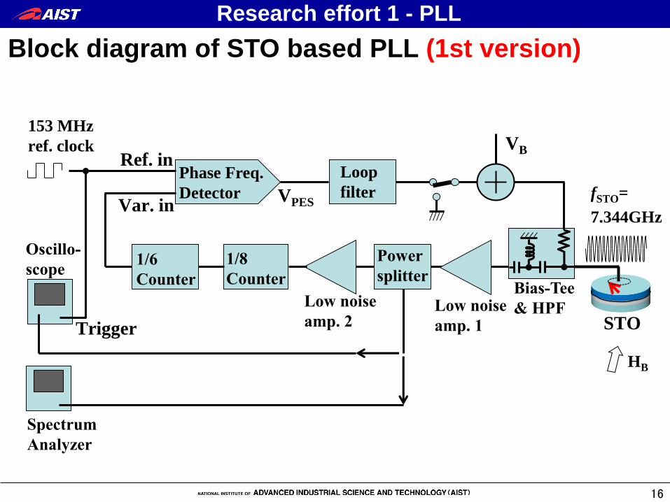
Ref. in
153 MHz
ref. clock
Phase Freq.
DetectorVar. in
VPES
Loop
filter
Bias-Tee
& HPF
HB
STOLow noise
amp. 1
1/8
Counter
1/6
Counter
fSTO=
7.344GHz
VB
Power
splitter
Spectrum
Analyzer
Low noise
amp. 2
Oscillo-
scope
Trigger
Block diagram of STO based PLL (1st version)
Research effort 1 - PLL

17
Research effort 1 - PLL
STO Based PLL 1st version
18
-50
-45
-40
-35
-30
-25
-20
-15
-10
-5
0
7.319 7.344 7.369
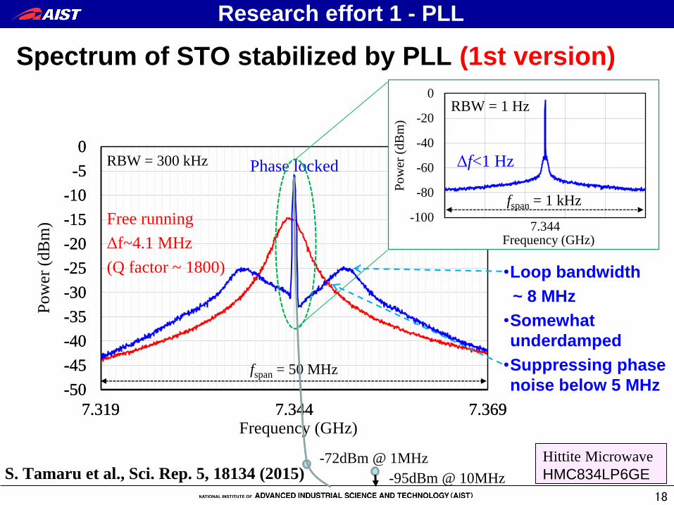
Spectrum of STO stabilized by PLL (1st version)
Frequency (GHz)
Pow
er (
dB
m)
fspan = 50 MHz
-50
-45
-40
-35
-30
-25
-20
-15
-10
-5
0
7.319 7.344 7.369
Phase locked
-100
-80
-60
-40
-20
0
Frequency (GHz)7.344
Po
wer
(d
Bm
)
RBW = 1 Hz
fspan = 1 kHz
Δf<1 Hz
Free running
Δf~4.1 MHz
(Q factor ~ 1800)
RBW = 300 kHz
-72dBm @ 1MHz
-95dBm @ 10MHz
Hittite Microwave
HMC834LP6GE
Research effort 1 - PLL
S. Tamaru et al., Sci. Rep. 5, 18134 (2015)
•Loop bandwidth
~ 8 MHz
•Somewhat
underdamped
•Suppressing phase
noise below 5 MHz

19
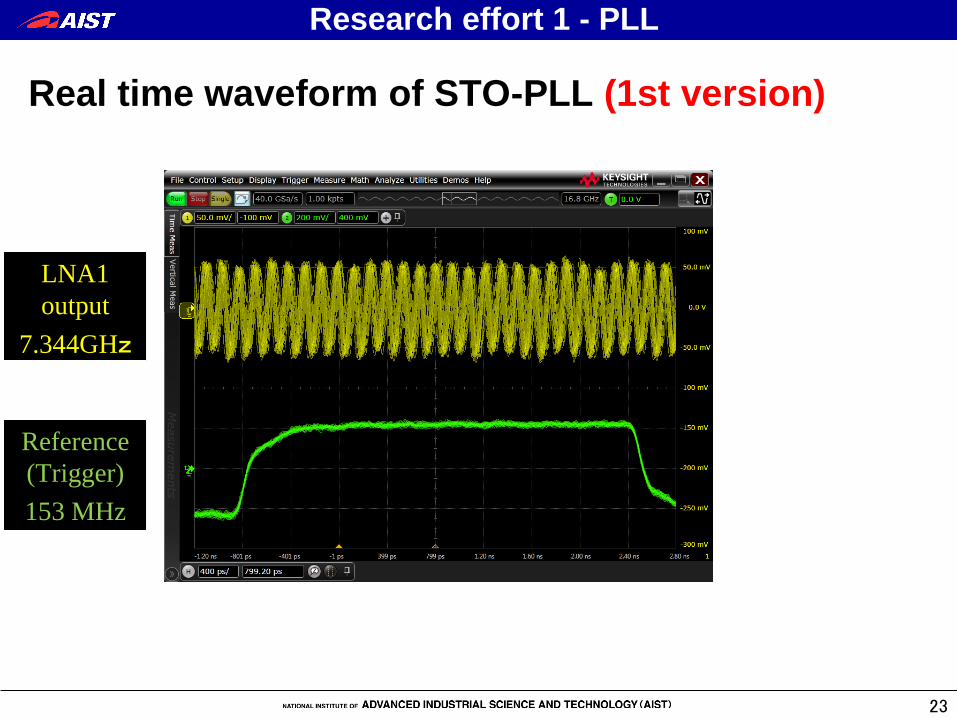
Real time waveform of STO-PLL (1st version)
Timing jitter
σ ~ 20 ps
Reference
(Trigger)
LNA1
output
Commercial
PLLs
σ ~ 0.2 ps
Research effort 1 - PLL

20
Research effort 1 - PLL
STO Based PLL 2nd version
21
Research effort 1 - PLL
-45
-40
-35
-30
-25
-20
-15
-10
-5
0
5
6.971 6.996 7.021
-45
-40
-35
-30
-25
-20
-15
-10
-5
0
5
6.971 6.996 7.021
Phase locked
Frequency (GHz)
Pow
er (
dB
m)
fspan = 50 MHz
Free running
Δf~4.7 MHz
(Q factor ~ 1500)
RBW = 300 kHz
Spectrum of STO stabilized by PLL (2nd version)
S. Tamaru et al., APEX, 9, 053005 (2016)
•Loop bandwidth
~ 16 MHz
(x2 wider than 1st ver.)
•Somewhat
underdamped
•Suppressing phase
noise below 10 MHz
(x2 wider than 1st ver.)

22
Research effort 1 - PLL
Reference
(Trigger)
251.5 MHz
LNA1
output
6.996GHz
Real time waveform of STO-PLL (2nd version)
23
Research effort 1 - PLL
Reference
(Trigger)
153 MHz
LNA1
output
7.344GHz
Real time waveform of STO-PLL (1st version)
24
Research effort 1 - PLL
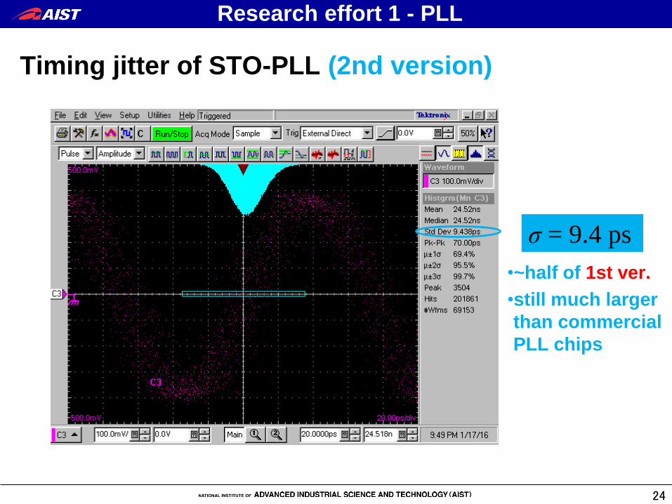
Timing jitter of STO-PLL (2nd version)
σ = 9.4 ps
•~half of 1st ver.
•still much larger
than commercial
PLL chips
25
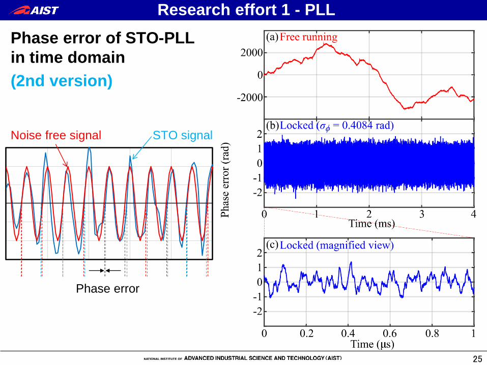
Research effort 1 - PLL
Phase error of STO-PLL
in time domain
(2nd version)
Noise free signal STO signal
Phase error

26
Research effort 1 - PLL
Phase error of STO-PLL
in frequency domain
(2nd version)
(top)
Power spectrum
of phase error
(bot.)
Power spectrum
of freq. fluctuation
(Calculated from
Sν = Sϕ / f 2)
Thermal
agitation
1/f fluctuation
(source
unknown)Relaxation
rate of
precession
trajectory
PLL’s
bandwidth
Unclear why it dosen’t
drop monotonically.
Free running
Phase locked
Free running
Phase locked

27
Research effort 1 - PLL
• Very difficult to build such a PLL circuit (i.e. a bandwidth >> 50 MHz).
• Even if we can, STO may not follow.
Phase error of STO-PLL
in frequency domain
(2nd version)
Magnified view
of phase error
• Up to 100 MHz
• Linear scale for
both x and y axes
Free running
Phase locked
How can we further reduce timing jitter? Simple scaling:
1/10 of timing jitter → 1/100 of total noise power → 100 higher Q factor
• Thermal agitation is the dominant noise source (1/f is negligible).
• 92.5% of total noise power is contained in this region.
• If this part were completely eliminated, total timing jitter would be 2.6ps.

28
Research effort 1 - PLL
Ref. in
291.5 MHz
ref. clock
Phase Freq.
DetectorVar. in
VPES
Loop
filter
Bias-Tee
& HPF
HB
STOLow noise
amp. 1
1/24
Counter
fSTO=
6.996GHz
VB
Power
splitter
Block diagram of STO-PLL
Requirements for frequencies in STO-PLL
6.996 GHz 291.5 MHz ~16 MHz 4.7 MHz
STO
frequency
Reference
frequency
Loop
bandwidth
STO
linewidth>> >> >>
This seems the only value that may be improved.

29
Research effort 1 - PLL
What about power?
Noise causes timing
error at down counter
Larger noise cause
counting error
S. Tamaru et al., submitted to JJAP (2016)

30
Research effort 1 - PLL
What about power?
Timing jitter caused by Johnson / shot noises
This result indicates that STO’s output power
has to be larger than -20 dBm (10 μW)!

31
Challenges in STOs
In order to use a STO for wireless communication,
We have to achieve,
• Output power on the order of 10 μW,
(Current world record: 2.5 μW @ 6.75GHz)Wang et al., JSAP Autumn Meeting, Nagoya, Japan (2015)
Quantitative analysis submitted to Jap. J. App. Phys.
• Q factor on the order of (perhaps) million,
(Current world record: ~3200 @ 15GHz for
MTJ-STO)Maehara et al., APEX 7.2, 023003 (2014)
Quantitative analysis now underway
These values look really formidable, don’t they?

32
Challenges in STOs
2. Challenges in using STOs for practical
microwave applications
2. Ultrahigh sensitivity FMR (I-FMR)

33
Challenges in STOs
Efforts to improve STO performance within AIST
• Better MTJ for higher MR ratio and lower RA
(Yakushiji et al.)
• Different STO structures (Kubota et al.)
• Phase locking of multiple STOs through
electrical connection (Tsunegi)
• Larger STO size (Tamaru)
• Search for new ideas (Everyone)

34
Why larger STO size? > For higher thermostability
But if we simply make a STO larger, what happens?
• Higher order modes excited
• Mode hopping
Challenges in STOs
Power spectral density of
STO as a function of VB
HB=257mT
Real time waveform
of STO signal
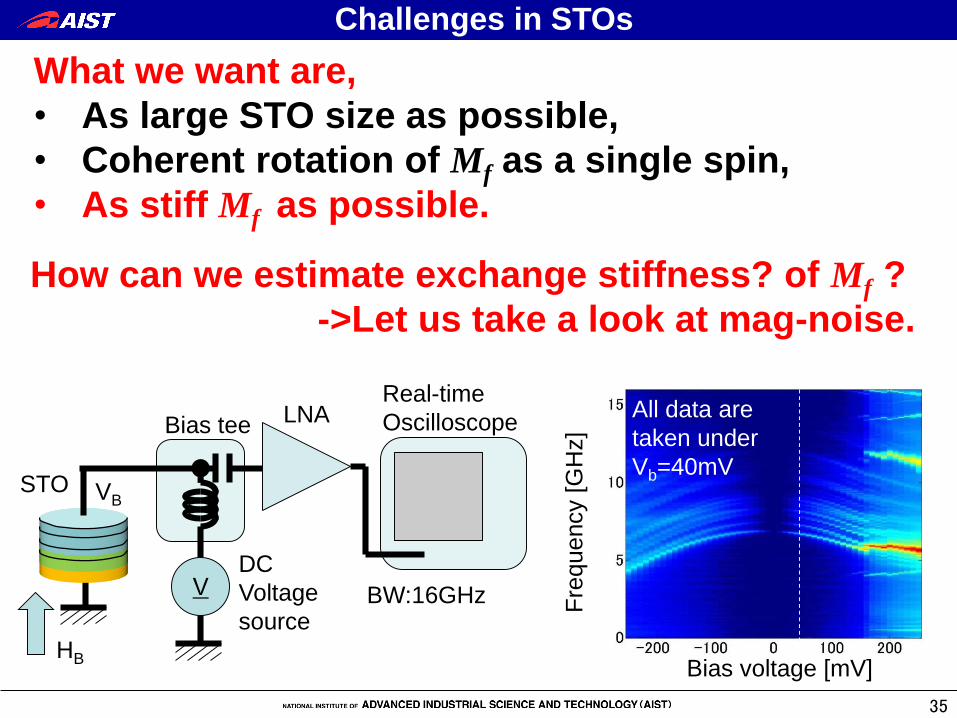
35
What we want are,
• As large STO size as possible,
• Coherent rotation of Mf as a single spin,
• As stiff Mf as possible.
Challenges in STOs
How can we estimate exchange stiffness? of Mf ?
->Let us take a look at mag-noise.
VB
-
Bias tee
DC
Voltage
source
V
LNA
BW:16GHz
Real-time
Oscilloscope
HB
STO
Fre
quency [
GH
z]
Bias voltage [mV]
All data are
taken under
Vb=40mV

36
Challenges in STOs
300nm
200nm
Log(W
) 100nm
Mag-noise spectra of three PMF-STOs
Wider mode intervals for smaller
STOs.
Mode frequencies shift linearly as
HB increases.
Spin wave resonances excited on
perpendicularly saturated free layer
AEX can be estimated from mode
intervalS. Tamaru et al., MMM Denver (2013)
37
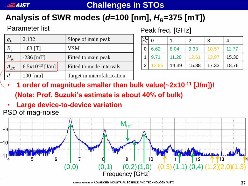
Challenges in STOs
Analysis of SWR modes (d=100 [nm], HB=375 [mT])
gL 2.132 Slope of main peak
BS 1.83 [T] VSM
HK -236 [mT] Fitted to main peak
AEX 6.5x10⁻¹³ [J/m] Fitted to mode intervals
d 100 [nm] Target in microfabrication
0 1 2 3 4
0 6.62 8.04 9.33 10.57 11.77
1 9.71 11.20 12.61 13.97 15.30
2 12.85 14.39 15.88 17.33 18.76
PSD of mag-noise
Peak freq. [GHz]
(0,0) (0,1) (0,2)(1,0) (0,3) (1,1) (0,4) (1,3)(1,2)(2,0)
Mref
Parameter list
• 1 order of magnitude smaller than bulk value(~2x10-11 [J/m])!
(Note: Prof. Suzuki’s estimate is about 40% of bulk)
• Large device-to-device variation
rc
Frequency [GHz]

38
Challenges in STOs
Some researchers I met in MMM2013 or in Japan
• The estimated AEX may be correct, judging from the good
agreement.
• Then what about other parameters affected by exchange
coupling, such as TC or domain wall thickness?
• Why does AEX vary for difference devices?
• How and why does Aex vary as a function of film thickness?
Prof. Slavin
• Shingo’s AEX should be wrong.
• Interlayer coupling should be taken into account.(J. Phys. Condens. Matter 22 (2010) 136001)
My decision:
I have to take out the free layer from STO and measure FMR!

39
Challenges in STOs
Conventional VNA-FMR setup
VNA
P1
S21
CPW
Magnetic dot
HRF
HB
P2
If the dot is small,• an array of dots is needed to compensate for low sensitivity.
• Q: Is the signal from an array the same as from one dot?
FMR on single nanodot is desirable!
But how can I achieve such a high sensitivity?
A: Not always.

40
Challenges in STOs
Ultrahigh sensitivity FMR based on microwave
interferometer (I-FMR)
VNA
P1
S21
CPW
Magnetic element
HRF
HB+HLF
P2 Rec.
Phase shifter Var. attenuator
Power
divider
Power
combiner
LNA
Tamaru et al. IEEE Magn. Lett., 5, 3700304 (2014)
41
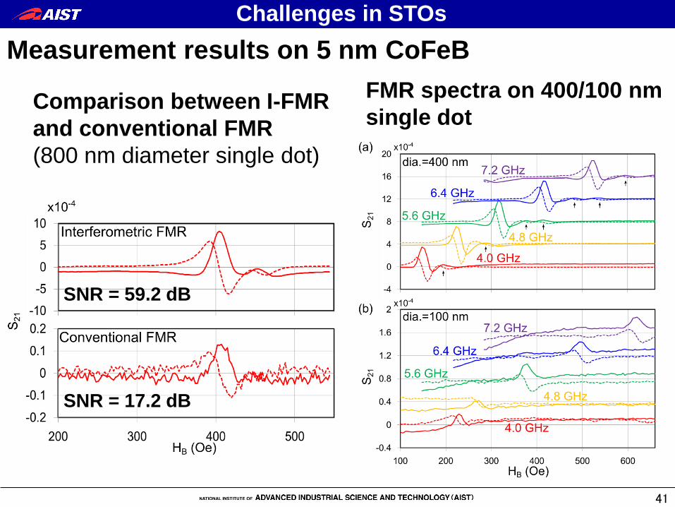
Measurement results on 5 nm CoFeB
FMR spectra on 400/100 nm
single dot
SNR = 59.2 dB
SNR = 17.2 dB
Comparison between I-FMR
and conventional FMR
(800 nm diameter single dot)
Challenges in STOs
42
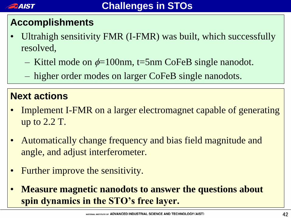
Accomplishments
• Ultrahigh sensitivity FMR (I-FMR) was built, which successfully
resolved,
– Kittel mode on f=100nm, t=5nm CoFeB single nanodot.
– higher order modes on larger CoFeB single nanodots.
Next actions
• Implement I-FMR on a larger electromagnet capable of generating
up to 2.2 T.
• Automatically change frequency and bias field magnitude and
angle, and adjust interferometer.
• Further improve the sensitivity.
• Measure magnetic nanodots to answer the questions about
spin dynamics in the STO’s free layer.
Challenges in STOs
43
Challenges in STOs
2. Challenges in using STOs for practical
microwave applications
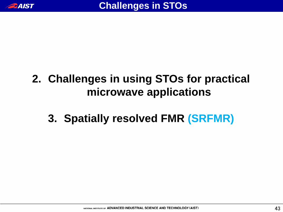
3. Spatially resolved FMR (SRFMR)

44
V. Demidov et al., Nat. Mater., 9, 984 (2010) M. Madami et al., Nat. Nanotechnol., 6, 635 (2011)
Direct observation of a propagating spin wave
induced by spin-transfer torque
Direct observation and mapping of spin waves
emitted by spin-torque nano-oscillators
AIST wants to see spin dynamics excited by STO oscillation
Challenges in STOs

45
Spatially resolved ferromagnetic resonance (SRFMR)
Is Microfocuse BLS the only solution to do this measurement? NO!
Challenges in STOs
Incident light
Bias field
Reflected light
Excitation field
Block diagram of SRFMR
Tamaru et al., JAP, 91, 8034 (2002)
1D profile of decaying plane MSSW
propagating on Py film
Tamaru et al., RPB, 70, 104416 (2004)
Spatial mode profiles of spin wave
eigenmodes on square Py film
Am
p.
Ph
ase
50
mm
Tamaru et al., JAP, 91, 8034 (2002)

46
Limitation
in SRFMR
Excitation frequency must be an integer multiple of the laser
repetition rate, which is fixed at 80 MHz in Ti:S mode-locked laser
New SRFMR
design goals
• Work at arbitrary frequencies between 20MHz-20GHz
• Detect in-plane dynamic magnetization
• Maintain high spatial resolution
Block diagram of new SRFMR
Semicon.
laser
PLL Freq.
synthesizer
Microwave
synthesizer
10MHz
Master clock
-
4.6KHz
Modulation
signal
Lock-in
amp.
Two-split
photo
detector
NPBS
Obj. lens
Sample
XY motorized
state
Trig. in
Ref. in.
Mod. in.
Ref. in.
Sig. inRef. in.
PPulse width: 25ps
Host PC
Challenges in STOs

47
Measurement of magnetostatic surface wave (MSSW)
Py Coupon
(100x100 mm2)
Coplanar waveguide
8 GHz
Drive Current
340 Oe
Bias field
Spin
Waves
Sample geometry
0-50 50-25 25
Position [mm]
Phase [
rad]
p
-p
0
-12
-16
-20
-24
-28Log(a
mplit
ude)
[arb
.]
Laser pulse rate: 40 MHz
Challenges in STOs

48
What are good about SRFMR?
• Much cheaper than MF-BLS,
• Comparable or higher sensitivity,
• Same spatial resolution (optical diffraction limited),
• Vectorial component detection,
• Good at relatively low frequencies (currently targeting
20MHz ~ 20 GHz), so that it can capture vortex dynamics,
• Easily converted to TR-MOKE,
• Phase sensitive.
Should be a powerful tool to study spin dynamics!
Challenges in STOs
49
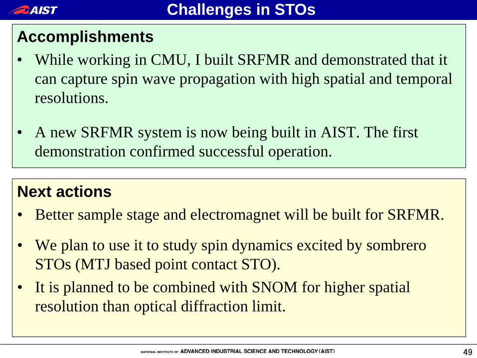
Accomplishments
• While working in CMU, I built SRFMR and demonstrated that it
can capture spin wave propagation with high spatial and temporal
resolutions.
• A new SRFMR system is now being built in AIST. The first
demonstration confirmed successful operation.
Next actions
• Better sample stage and electromagnet will be built for SRFMR.
• We plan to use it to study spin dynamics excited by sombrero
STOs (MTJ based point contact STO).
• It is planned to be combined with SNOM for higher spatial
resolution than optical diffraction limit.
Challenges in STOs

50
3. Summary
Summary
51
Summary
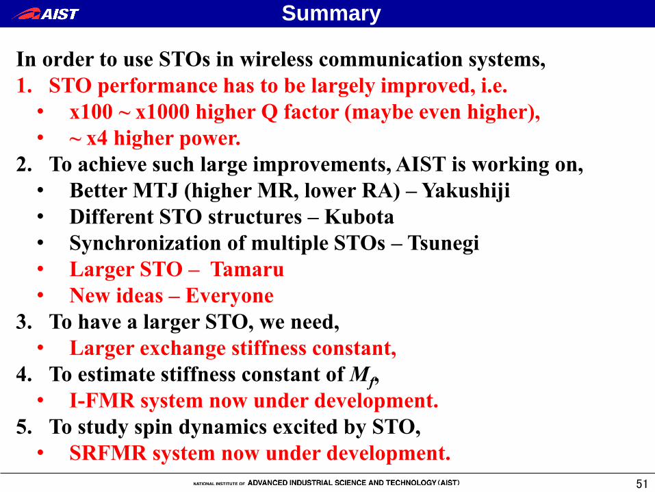
In order to use STOs in wireless communication systems,
1. STO performance has to be largely improved, i.e.
• x100 ~ x1000 higher Q factor (maybe even higher),
• ~ x4 higher power.
2. To achieve such large improvements, AIST is working on,
• Better MTJ (higher MR, lower RA) – Yakushiji
• Different STO structures – Kubota
• Synchronization of multiple STOs – Tsunegi
• Larger STO – Tamaru
• New ideas – Everyone
3. To have a larger STO, we need,
• Larger exchange stiffness constant,
4. To estimate stiffness constant of Mf,
• I-FMR system now under development.
5. To study spin dynamics excited by STO,
• SRFMR system now under development.
52
Summary
I think it is time for every one of
us to get together and propose
new ideas to overcome these
difficulties in order to make
STOs useful for human society.
Any comment on this talk is
highly appreciated!