Embed Size (px)
Citation preview
CHALLENGES IN EMBEDDED MEMORY DESIGN AND TESTHistory and Trends In Embedded System Memory
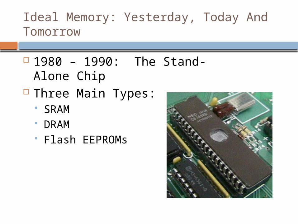
Ideal Memory: Yesterday, Today And Tomorrow
1980 – 1990: The Stand-Alone Chip
Three Main Types: SRAM DRAM Flash EEPROMs
1980-1990: The Stand-Alone Chip
SRAM – The “S” is for “Static” 6T variety used in handheld systems due
to: Low standby power Wide noise margin Ease of use
4T variety typically used for cache, especially for systems using mostly DRAM
1980-1990: The Stand-Alone Chip
DRAM – The “D” is for “Dynamic” Must be refreshed periodically because the
bits are stored with a capacitor, which leaks current
Small cell size and high density made them ideal for larger memory systems.
However, slower performance typically required the use of an SRAM cache
Higher power consumption due to the need for refreshing, not suitable for handheld embedded systems.
1990-2000: Memory Integrated With Logic
From 1990-2000, logic began to be integrated onto memory chips
Sub-micron processes increased logic speed, requiring faster memories
Also provided room for logic on the memory chip, allowing them to be synchronous
Refresh circuitry for DRAMs now located on chip, allowed them to operate in an SRAM socket (P-SRAM, “P” stands for “Pseudo”)
2000-2005: Scaled Embedded Memory
Era of true embedded memory begins 100’s of millions of gates on a chip allows
for a large portion of chips to contain memory that are functionally not a memory
Embedded memory has different characteristics than standalone memory: Wide on-chip buses + parallelism High-speed operation not as important
Commercial IP becomes equivalent of a memory standard
The Product Perspective: Trends in SoC Design
Memory content in SoC increasing dramatically from year to year.
Memory either organized as large chunks of “hand optimized” blocks or smaller memories generated by compilers.
Re-used logic and memory blocks exceed number of newly designed functions Why? Designs are stable faster allowing
device manufacturers to meet a faster market window
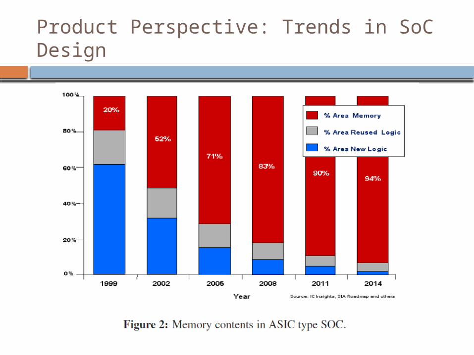
Product Perspective: Trends in SoC Design
Advantages and Challenges To Embed Memories
Why embed all this memory? If tailored properly you can achieve:
Improved performance Lower power consumption On-demand memory activation / refined stand-
by modes Higher bandwidth Package cost reduction and overall cost
reduction Generalized form factor / board space
advantages
Advantages and Challenges To Embed Memories
BUT: Drawbacks vs. using multiple chips Increased development complexity Memories need to be area optimized Need new design methodologies Need new testing methodologies Higher mask cost Higher effort to ramp one complex product Decreased flexibility and extendibility
Implementation of Embedded Memory Devices: A Case Study
Need to develop a communication device with the following requirements: Doubled Functionality 30% Performance Gain Compared To Multi-
Device Solution Power must be optimized so that the device
still fits into its former package
Implementation of Embedded Memory Devices: Case Study
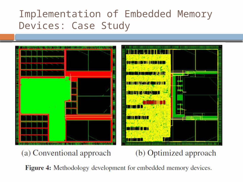
Only solution was to embed all memory: Multi-chip failed: Off-chip driver for the
larger memories absorbed 30% of power budget alone
Need a customized floor plan where logic placement was optimized with respect to memory location.
I.E. More than just sticking a big blob of SRAM on the chip somewhere
Implementation of Embedded Memory Devices: Case Study
Embedded Memory Test and Repair: Trends and Challenges
Today’s SoCs have moved from being logic-dominant to memory dominant
More memory needed for today’s memory hungry applications
Aggressive design of embedded memories leads to greater manufacturing and field reliability problems than any other part of the chip
Overall yield thus relies heavily on the memory yield, significantly affecting cost
Embedded Memory Test and Repair: Trends and Challenges
Yield can be improved by offering redundancy in memories
Requires determining the adequate type and amount from memory design techniques and failure history
Further, need ability to detect where defects occur and knowledge of how to then incorporate redundant elements
Test and Repair Power-Up Soft Repair
Manufacturing Cost
Traditional approach of Test-and-Repair requires extensive equipment and can contribute as much as 40% of the overall manufacturing cost of a chip
Need to keep these costs down especially for high-volume consumer electronics or anything that is particularly cost-sensitive.
Time-To-Volume
Time-To-Volume is the time it takes a design to become sufficiently mature such that it can be manufactured in high volume at lower cost
Dependent upon two factors: Initial SoC design time
Re-use of proven IP cores Production ramp-up time
Yield optimization: detect, analyze and correct problems
Time-To-Volume
Time-to-market pressure may require a shortened ramp-up period
Can minimize TTV if yield optimization starts before ramp-up period Memory IP cores need to be tested in silicon and
optimized beforehand to improve yield once incorporated into an SoC: “Silicon-Proven IP”
Memory IP should already include all necessary diagnosis and failure analysis functions which can then be used during ramp-up
Memory repair functions need to be designed together with the system as a whole to simplify the SoC ramp-up.

Questions