Embed Size (px)
Citation preview

Challenges and Opportunities with
Place and Route of
Modern FPGA Designs
Raymond Nijssen
VP of Systems Engineering
Achronix Semiconductor, Santa Clara, CA
ISPD 2016

Acknowledgements
Mike Riepe
Dan Pugh
Amit Singh
2
4/4/2016
ISPD 2016 (c) Achronix Semiconductor Corp.

Evolution of FPGA place and route systems
• FPGA place and route CAD has evolved rapidly in the last 10-15
years
• Initial FPGA EDA flows were fairly unsophisticated compared to
ASIC flows.
• Design sizes were small enough to permit slower algorithms
• Focus was on making the user design fit
• What has changed ?
• Modern FPGA designs can have 5M placeable objects
• Fast runtimes are competitive make-or-break criteria
• Extreme QoR pressure to maximize performance
• FPGA EDA flows now employ P&R algorithms first employed in
ASIC flows.
4/4/2016
3 ISPD 2016 (c) Achronix Semiconductor Corp.

Key Differences between ASIC and FPGA
design flows
• No parasitics extraction,
• No on-the-fly delay calculation
• No cell sizing
• No buffering
• Specialized clock routing
• No power routing (coming, but not as we know it)
• No nasty design rules
• No antenna rule fixing
• No global routing (*)
• What’s left ?
• RTL Synthesis, TD P&R, STA, GUI, IP configurators, Bitstream gen…
4/4/2016
4 ISPD 2016 (c) Achronix Semiconductor Corp.

The Straightjacket
• The FPGA itself is a design
• EDA for FPGAs == fitting a (user) design within a (FPGA) design.
• Solution space is highly discrete (non-continuous)
• FPGA itself is pre-designed consisting of small number of different resource types
• LUT
• ALU chains
• FF’s
• Various sizes of embedded memories
• Special logic building blocks: DSP
• MUXes
• Resource types have fixed locations
• Clocks cannot be freely routed
• Limited number of clock resources per area
• Few different type routing resources
• No smooth trade-offs: no cell sizing, buffering etc.
4/4/2016
5 ISPD 2016 (c) Achronix Semiconductor Corp.

FPGA Logic Tile Simplified Example
Many connections omitted for clarity
Programmable input and output crossbar switches not shown
Synthesis converts user RTL to netlist of these primitives
4/4/2016
6 ISPD 2016 (c) Achronix Semiconductor Corp.

Multi-Resource Placement
• Locally varying resource utilization not correlated between
resource types
• Supply vs Demand must be modeled per-resource type
• Overlapping density maps for different types
• Density maps are loosely and strongly related at the same time….
• Conflicting de-overlap gradients pose challenging placement
convergence problems
• Example:
• In some area, LUT utilization may be high, while FF utilization is low
• Timing-critical FF gets pulled into low-FF utilization area
• but associated LUTs cannot be legalized there due to high LUT utilization
• Pre-clustering often used to sidestep this
• Cyclical dependency: post-placement timing criticality is hard to predict
4/4/2016
7 ISPD 2016 (c) Achronix Semiconductor Corp.

Special Resources are few and far between
• Block Ram, Local Ram and DSP
resources are spread out across
core area
• Moving any of these creates often
very disruptive to convergence
• Generic modeling required in
algorithms to support multiple
different FPGA fabrics
4/4/2016
8 ISPD 2016 (c) Achronix Semiconductor Corp.
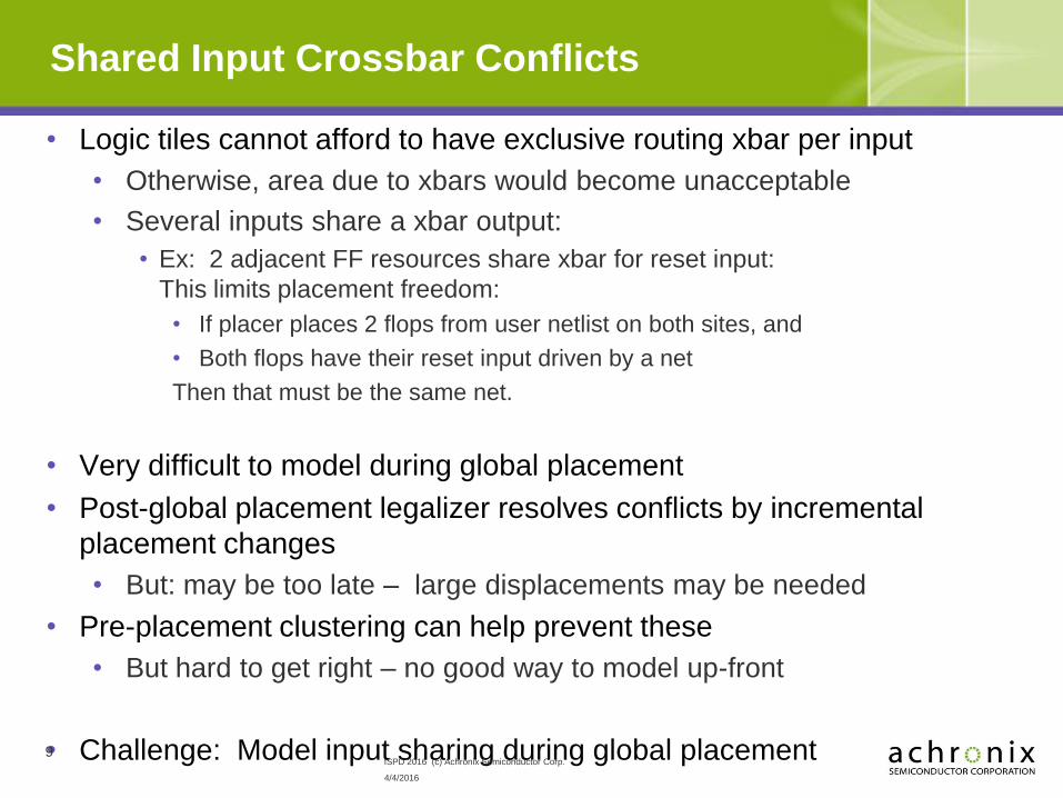
Shared Input Crossbar Conflicts
• Logic tiles cannot afford to have exclusive routing xbar per input
• Otherwise, area due to xbars would become unacceptable
• Several inputs share a xbar output:
• Ex: 2 adjacent FF resources share xbar for reset input:
This limits placement freedom:
• If placer places 2 flops from user netlist on both sites, and
• Both flops have their reset input driven by a net
Then that must be the same net.
• Very difficult to model during global placement
• Post-global placement legalizer resolves conflicts by incremental
placement changes
• But: may be too late – large displacements may be needed
• Pre-placement clustering can help prevent these
• But hard to get right – no good way to model up-front
• Challenge: Model input sharing during global placement
4/4/2016
9 ISPD 2016 (c) Achronix Semiconductor Corp.

Carry Chains formed by vertical tile concatenation
• Carry chains are very fast
• Great for implementing wide logic
• Counters
• Wide AND/OR
• Comparators
• Etc
• Limitations:
• Can get long (eg. 64 bits or more)
• Must be placed in contiguous way
• Can run in only 1 direction
• Share inputs with other logic in the
tile
4/4/2016
10 ISPD 2016 (c) Achronix Semiconductor Corp.

Carry Chain Legalization
11
4/4/2016
ISPD 2016 (c) Achronix Semiconductor Corp.
1. Global Placer determines approximate area for each carry chain 2. Carry Chain Legalizer must transitively nudge carry chains around :
• Guarantee overlap-free assignment to FPGA resources within given placement region
• Minimize max displacement • Moving other resources with moving carry chains • Obeying pre-placed logic • Minimize WNS
Solution space is very non-smooth, full of poor local minima Challenge: Model carry chain legalizability during global placement
•Green bar: carry
chain
•Red bar: fixed block
RAM
•Grey: LUTs and FFs

Global to Legal Placement Delta
12
4/4/2016
global legal
Red dot: placement overlap Red line: instance displacement by legalizer
ISPD 2016 (c) Achronix Semiconductor Corp.

Carry Chain Placement Challenge
•Designs will contain carry chains with different lengths • Length heterogeneity greatly complicates fitting
• Especially in high-carry chain utilization areas • Often carry chains span many tiles vertically
• Carry chains are heavily connected to other logic and carry chains • Any movement is a great disruption to placement and timing closure • Very unpredictable
• Carry Chains tend to “snap” to far-away locations
• How to do better ? • Placement algorithm combined with FPGA architectural innovations welcome !
4/4/2016
13 ISPD 2016 (c) Achronix Semiconductor Corp.

Trend: Modern FPGAs have high IO Bandwiths
Example:
Achronix 22nm FinFET FPGA
In volume production since 2015
Programmable logic core
interfaces with many very-high
speed IOs
• 64x 10Gbps SerDes
• 2x 100 Gbps Ethernet
• 2x 100 Gbps Interlaken
• 2x 64 Gbps PCIe Gen3x8
• ~1000x 1.6 Gbps GPIO
• 6x DDR3@1600 x72
Protocol controllers hardened as
ASIC blocks around FPGA core
4/4/2016
14 ISPD 2016 (c) Achronix Semiconductor Corp.

3.12 6.25
12.5
25
50
100
0
20
40
60
80
100
120
90 65 28 16 7 5
Peak SerDes line rate (Gpbs) per lane
Normalized effective per-LUT delay
Historical and
projected
trends
Technology node (nm)
Network Line Rates Accelerate on Hyper-Moore Curve
Per-lane SerDes IO data rates increases > 1.5x per technology node
Logic and interconnect delay reductions not keeping up…..
User-design architectural response:
“Just double the parallel datapath width” ….
FPGA Architectural improvements mitigate gap somewhat
15
4/4/2016
ISPD 2016 (c) Achronix Semiconductor Corp.

22nm FPGA 100 Gbps Ethernet Interface Architecture
16
SerDes SerDes SerDes
1010110
…
1010110…
1010110
…
1010110…
1010110
…
1010110…
100 GbE MACPCS
SerDes lane
aggregation:
10x10Gbps
or
4x25Gbps
FPGA core with user design
Typical Fmax <300 MHz
N-byte wide
word parallel
bus interface.
• 100.0% sustained bandwidth must be guaranteed
• Under any circumstance
• Requires certain minimum required frequency on N-byte i/f 4/4/2016
ISPD 2016 (c) Achronix Semiconductor Corp.

Widening Parallel Data Path to Reduce its Frequency
Requirement:
Bandwidth of parallel data path > SerDes line rate
Traditional FPGA user logic in practice should not target
frequencies > 300 MHz.
Faster is possible with careful coding and user-level pipelining.
… but most designers won’t be productive
Bus_bandwidth = bits_per_word * clock_frequency
So, in order to guarantee minimum bandwidth: widen the
datapath until Fmax low enough in practice.
17
4/4/2016
ISPD 2016 (c) Achronix Semiconductor Corp.

100 Gigabit Ethernet Parallel Bus Requirements
18
When bus width is doubled, min required frequency does not get halved
N-byte
bus size
(Bytes)
ACTUAL
minimum
required
clock rate
(MHz)
IDEAL
minimum
required
clock rate
(MHz)
8 1550 1550
16 779 775
32 442 388
64 295 194
96 214
128 168 97
256 149 49
512 149 25
100
200
400
800
1600
8 16 32 64 128 256 512
MINIMUM REQUIRED CLOCK RATE (MHz)
Ideal parallel bus bandwidth (Gbps)
FPGA design practical Fmax (MHz)
Line rate bandwidth (Gbps)
bytes
4/4/2016
ISPD 2016 (c) Achronix Semiconductor Corp.
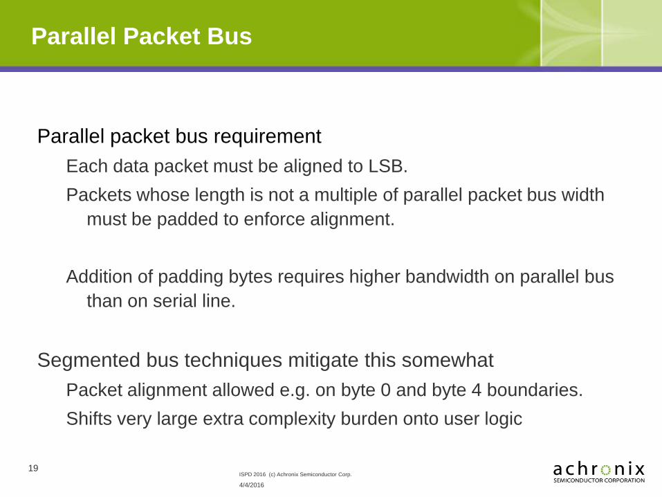
Parallel Packet Bus
Parallel packet bus requirement
Each data packet must be aligned to LSB.
Packets whose length is not a multiple of parallel packet bus width
must be padded to enforce alignment.
Addition of padding bytes requires higher bandwidth on parallel bus
than on serial line.
Segmented bus techniques mitigate this somewhat
Packet alignment allowed e.g. on byte 0 and byte 4 boundaries.
Shifts very large extra complexity burden onto user logic
19
4/4/2016
ISPD 2016 (c) Achronix Semiconductor Corp.
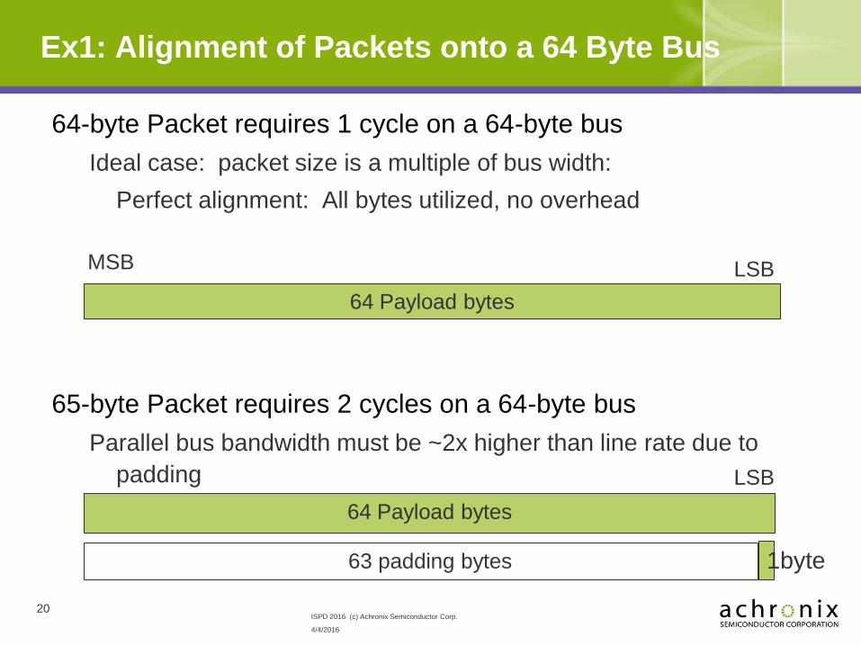
Ex1: Alignment of Packets onto a 64 Byte Bus
64-byte Packet requires 1 cycle on a 64-byte bus
Ideal case: packet size is a multiple of bus width:
Perfect alignment: All bytes utilized, no overhead
65-byte Packet requires 2 cycles on a 64-byte bus
Parallel bus bandwidth must be ~2x higher than line rate due to
padding
20
64 Payload bytes
1byte 63 padding bytes
64 Payload bytes
LSB
LSB MSB
4/4/2016
ISPD 2016 (c) Achronix Semiconductor Corp.

Required Minimum Bus Frequency
for 100GbE over 64-Byte Bus
21
100
150
200
250
300
64
90
116
142
168
194
220
246
272
298
324
350
376
402
428
454
480
506
532
558
584
610
636
662
688
714
740
766
792
818
844
870
896
922
948
974
1000
1026
1052
1078
1104
1130
1156
1182
1208
1234
1260
1286
1312
1338
1364
1390
1416
1442
1468
1494
Minimum Parallel Bus Frequency (MHz) due to Packet Size (Bytes)
4/4/2016
ISPD 2016 (c) Achronix Semiconductor Corp.

Ex2: Alignment of Packets onto a 128 Byte Bus
64-byte Packet requires 1 cycle on a 128-byte bus
Again, parallel bus bandwidth must be ~2x higher than line rate due
to padding
With segmentation, 2 subsequent packets could be packed in
one 128 Byte word
Again at the expense of increased complexity
22
64 padding bytes 64 Payload bytes
LSB MSB
4/4/2016
ISPD 2016 (c) Achronix Semiconductor Corp.

400 Gigabit Ethernet Parallel Bus Requirements
23
N-Byte bus
size
(bytes)
ACTUAL
minimum required
clock rate (MHz)
8 6197
16 3115
32 1765
64 1177
96 854
128 672
256 596
512 596
100
200
400
800
1600
3200
8 16 32 64 128 256 512
MINIMUM REQUIRED CLOCK RATE (MHz)
Ideal parallel bus bandwidth (Gbps)
FPGA design practical Fmax (MHz)
Line rate bandwidth (Gbps)
bytes
Naive doubling of bus width alone cannot reduce clock parallel bus frequency to
currently practicable rates 4/4/2016
ISPD 2016 (c) Achronix Semiconductor Corp.

External Memory Bus Width vs Internal Bus Width
DDR3/4 transaction sizes are multiples of 64 (w/o ECC) or 72 (w/ ECC) Bytes
No wide bus bandwidth breakdown due to alignment
Until internal bus width > 64 Bytes (ie. > 512 bits) -- impact application dependent
Very wide busses required in FPGA core to match external memory bus BW
Complex design architectural measures being employed to mitigate effect
partially
Increasing practically achievable core logic Fmax incrementally is insufficient 24
100
200
400
800
1600
144 288 576 1152
Fmin (MHz) x72 DDR4@3200 Mbps
Fmin (MHz) x72 LPDDR4@4266 Mbps
Fmin (MHz) x72 DDR4@2400 Mbps
Fmin (MHz) x72 DDR3@1600 Mbps
Practical Fmax (MHz)
Internal bus width to FPGA core (bits)
4/4/2016
ISPD 2016 (c) Achronix Semiconductor Corp.

The External IO Bandwidth Explosion Challenge
Summary:
• Increasingly poor return on huge resource expense for little
frequency reduction
• Widening busses does not even help to sufficiently lower
interface frequency to practically acceptable level
• Implementing extremely wide busses is very challenging in
FPGAs
• Very wide logic functions required
• > 2000 bit wide carry chains ?
• Worse: logic gets spread far apart
• Introduces very long wires with extra timing closure challenges
despite lower frequency.
• Resource usage increase with such busses is unacceptable
25
4/4/2016
ISPD 2016 (c) Achronix Semiconductor Corp.

Simply Exchanging Fast & Narrow for Slow
& Wide is Coming to an End
Low Resource Usage
Fast Resources needed
26
High Resource Usage
Slow Resources suffice 4/4/2016
ISPD 2016 (c) Achronix Semiconductor Corp.

Impact
• Extremely wide logic will become commonplace
• Even longer carry chains than today
• Placement-driven splitting and/or folding
• Various sequential optimizations:
• Useful clock skew
• HW support required
• On-the-fly retiming during P&R
• Maybe use time borrowing through latches
• Heavy Pipelining of FPGA architecture
• Requires much more pervasive and complex clocking infrastructure
• E.g. Use pulse latches in interconnect, cf. Altera Stratix 10
• Or go entirely asynchronous: e.g. Achronix PicoPIPE technology > 1 GHz.
• Radical FPGA architecture innovations to reduce average interconnect delays
This is driving majority of current and future FPGA P&R innovation and development 27
4/4/2016
ISPD 2016 (c) Achronix Semiconductor Corp.

Total Bandwidth of SerDes IO in&out of FPGA Core
Increasing #SerDes
lanes per FPGA vs
technology node
This is a multiplier on
top of per lane BW
Ex: Modern FPGA with 64 full duplex 10Gbps SerDes lanes
Total SerDes BW in & out of FPGA core > 1 Tbps
~ 106 simultanous HD video streams
Soon available: > 10 Tbps per FPGA
28
4/4/2016
ISPD 2016 (c) Achronix Semiconductor Corp.

Incremental Flow
• Users of FPGA flows demand “incremental P&R” flows
• When small part of design logic is changed, change only small part
of P&R solution
• Goals:
1. Must-Have: Preserve known-good results from previous runs
• Only change P&R of logic that changed / got added / etc.
• This is to minimize flow iterations
2. Nice-to-Have: reduce flow runtime
• Depends on how much got changed, what and where
• How to surgically remove and replace chunks of logic ….
• With no or minimum displacement of not-changed logic
• With no or minimum rip-up & re-route of not-changed logic
4/4/2016
29 ISPD 2016 (c) Achronix Semiconductor Corp.
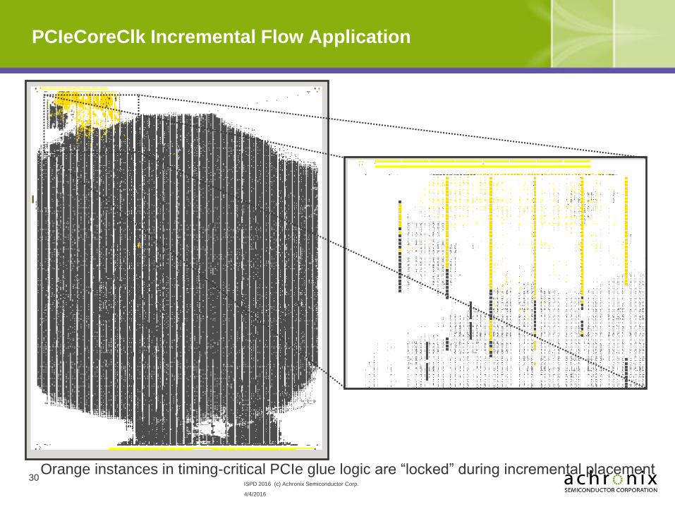
PCIeCoreClk Incremental Flow Application
30 Orange instances in timing-critical PCIe glue logic are “locked” during incremental placement
4/4/2016
ISPD 2016 (c) Achronix Semiconductor Corp.

Application: Find Best Solution for each Clock Domain,
Freeze it for all subsequent runs if not changed
Implementation clock name fMax
impl_1 PCIeCoreClk 435.7 MHz
impl_2 PCIeCoreClk 425.0 MHz
impl_3 PCIeCoreClk 432.9 MHz
impl_4 PCIeCoreClk 405.2 MHz
impl_5 PCIeCoreClk 390.8 MHz
impl_6 PCIeCoreClk 442.5 MHz
impl_7 PCIeCoreClk 411.8 MHz
impl_8 PCIeCoreClk 413.6 MHz
impl_9 PCIeCoreClk 420.6 MHz
impl_10 PCIeCoreClk 386.2 MHz
Implementation clock name fMax
impl_1 PCIeCoreClk 442.5 MHz
impl_2 PCIeCoreClk 442.5 MHz
impl_3 PCIeCoreClk 442.5 MHz
impl_4 PCIeCoreClk 442.5 MHz
impl_5 PCIeCoreClk 442.5 MHz
impl_6 PCIeCoreClk 442.5 MHz
impl_7 PCIeCoreClk 442.5 MHz
impl_8 PCIeCoreClk 442.5 MHz
impl_9 PCIeCoreClk 442.5 MHz
impl_10 PCIeCoreClk 442.5 MHz
31
PCIeCoreClk Target = 425.0 MHz. • The best PCIe related logic implementation (impl_6) was selected from the multiprocess run • Copied into all other implementations, and • Re-compiled incrementally. Note that the PCIeCoreClock timing remained identical in the second compile. This is because the placement and routing were locked.
4/4/2016
ISPD 2016 (c) Achronix Semiconductor Corp.

Achronix Semiconductor Corporation Confidential Information © 2014
.v .prt
prep
place
route
acxdb
acxdb
acxdb
.v’ .prt
incr. prep tear+stitch
incr. place
incr. route
acxdb
acxdb
acxdb
incremental netlist changes
typical
optional
optional
Incremental Flow:
“reference run” to “incremental run”
32

Typical Problem Example: Placement Trap.
Incremental run ends with 185 overflows.
33
Yellow: Frozen Placement
Grey: Incrementally added logic
Routed solution: overflows that
cannot be resolved without
moving added logic far away 4/4/2016
ISPD 2016 (c) Achronix Semiconductor Corp.

Incremental Flow Challenges
• Current incremental flow offers
• Stable QoR
• Practical runtimes
But: Surprise non-feasibility happens occasionally
• Router runtime challenge
• Difficult trade-offs between preserving existing routes and finding
good paths for new nets quickly
• Placement challenge: traps difficult to model
• How to nudge existing logic minimally to make room for new logic ?
4/4/2016
34 ISPD 2016 (c) Achronix Semiconductor Corp.

Thank You !
35
4/4/2016
ISPD 2016 (c) Achronix Semiconductor Corp.