Embed Size (px)
Citation preview
ELE 3230 - Chapter 6 1
Chapter 6 8284 Clock Generator
Bus Demux Bus Cycle
(Brey: ch8; Hall: ch7)
ELE 3230Microprocessors and Computer
Systems
ELE 3230 - Chapter 6 2
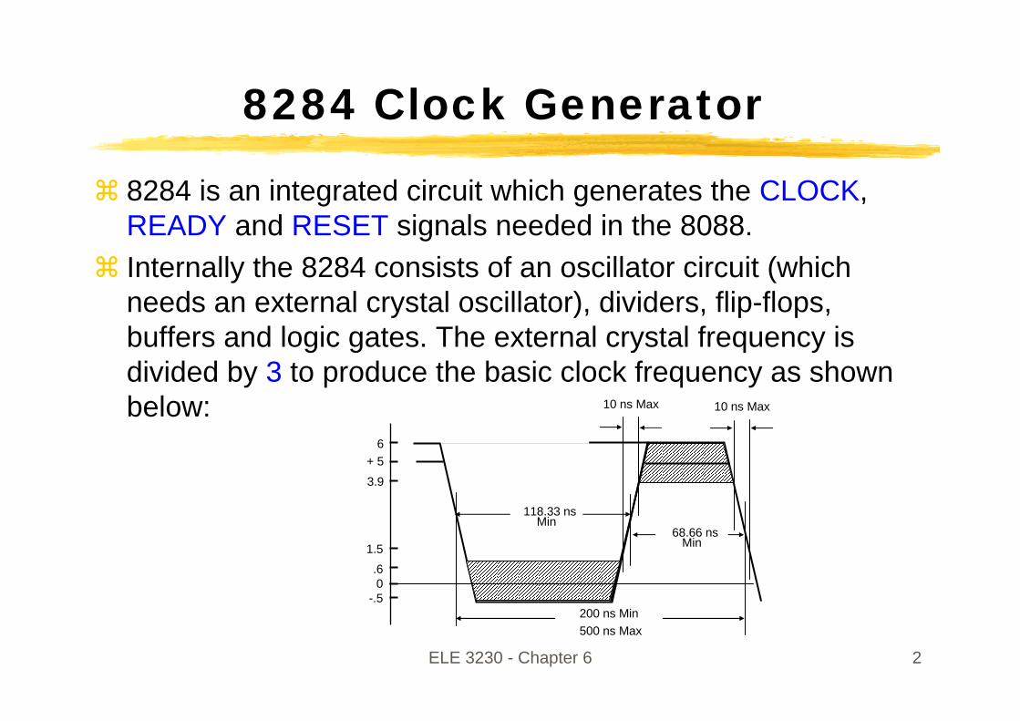
8284 Clock Generator
8284 is an integrated circuit which generates the CLOCK, READY and RESET signals needed in the 8088.Internally the 8284 consists of an oscillator circuit (which needs an external crystal oscillator), dividers, flip-flops, buffers and logic gates. The external crystal frequency is divided by 3 to produce the basic clock frequency as shown below:
200 ns Min500 ns Max
6+ 5
3.9
1.5.6 0
-.5
10 ns Max 10 ns Max
118.33 ns Min
68.66 ns Min
ELE 3230 - Chapter 6 3
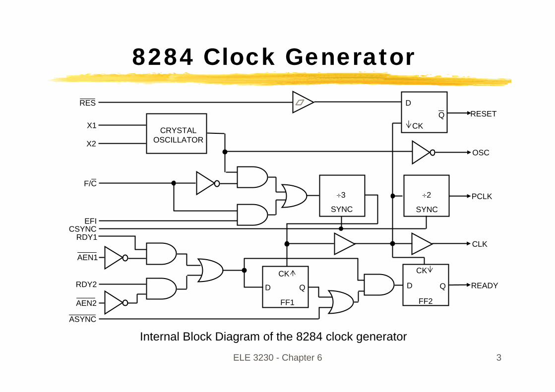
8284 Clock Generator
Internal Block Diagram of the 8284 clock generator
EFI
D
CKQ RESET
RES
÷3
SYNC
÷2
SYNCPCLK
F/C
RDY1
AEN1
RDY2
AEN2
READY
CK
D Q
FF2
CK
D Q
FF1
ASYNC
CRYSTAL OSCILLATOR
OSC
X1
X2
CLK
CSYNC
ELE 3230 - Chapter 6 4
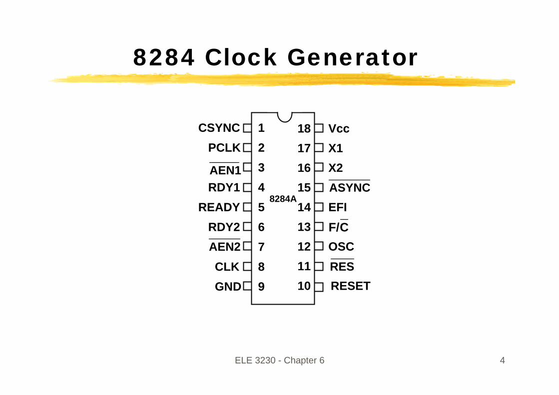
8284 Clock Generator
CSYNC 1PCLK 2
3RDY1 4
READY 5RDY2 6
7CLK 8GND 9
18 Vcc17 X116 X21514 EFI1312 OSC1110 RESET
8284A
CF/
ASYNC
RES
AEN1
AEN2
ELE 3230 - Chapter 6 5
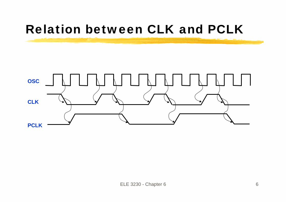
8284 Output PinsPCLK - peripheral clock; outputs clock signal which is at half the frequency of the main CLK output.
CLK – clock; outputs a 33% duty cycle periodic clock which runs at one third the frequency as the EFI or crystal frequency.
OSC - oscillator output; provides a buffered periodic waveform running at the crystal frequency. Output is suitable for driving the EFI input of another 8284.
RESET - generates an output suitable for the reset input of the 8088.
READY - generates READY signal suitable for 8088 READY input.
ELE 3230 - Chapter 6 6
Relation between CLK and PCLK
OSC
CLK
PCLK
ELE 3230 - Chapter 6 7
8284 Input PinsVCC, GND - power supply pins
RDY1 and RDY2 - bus ready, accepts input of the bus ready signal
AEN1, AEN2 - address enable (qualifies RDY1 and RDY2)
- ready synchronization select (selects one or two stages of synchronization for the RDY1 and RDY2 inputs
X1, X2 - crystal inputs (for connection of external clock signal input)
EFI - external frequency input (external clock signal input)
CSYNC - clock synchronization used with the EFI to synchronize the clock output in multiprocessor systems. MUST BE GROUNDED if the crystal oscillator is used.
- frequency/crystal (selects crystal oscillator or EFI as source)
- reset input (accept input from a switch for generating reset)
ASYNC
F/C
RES
ELE 3230 - Chapter 6 8
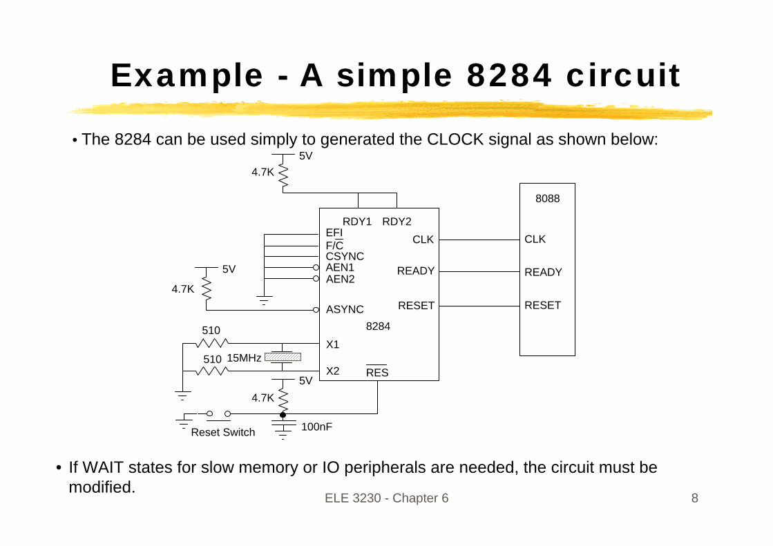
Example - A simple 8284 circuit
• If WAIT states for slow memory or IO peripherals are needed, the circuit must be modified.
• The 8284 can be used simply to generated the CLOCK signal as shown below:5V
5V
5V
RDY1 RDY2EFIF/CCSYNCAEN1AEN2
ASYNC
X1
X2 RES
RESET
READY
CLK
8284
RESET
READY
CLK
8088
Reset Switch 100nF
4.7K
4.7K
4.7K
510
510 15MHz
9
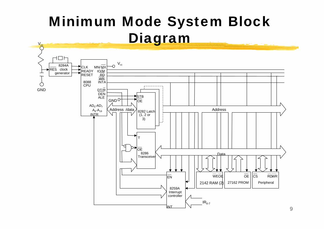
Minimum Mode System Block DiagramVcc
Vcc
GND
GND
Address /data Address
Data
IR0-7
CLK MXMN/READY MIO/RESET RD
WR8088 INTACPU
RDT/DENALE
A8-A19INTR
T
OE8286
Transceiver
EN
8259AInterruptcontroller
INT
STBOE
8282 Latch(1, 2 or
3)
WEOE
2142 RAM (2)
OE
27162 PROM
CS WRRD
Peripheral
8284ARES clock
generator
AD0-AD7
ELE 3230 - Chapter 6 10
Demultiplexing the Address and Data Bus
Address and data bus are multiplexed in 8086 (AD0-AD15) and 8088(AD0-AD7) to reduce the number of pins required.
Address and Data need to be demultiplexed from the bus. (Q: Why not leave it multiplexed?)
How to maintain a stable address throughout a read or write cycle?
ELE 3230 - Chapter 6 11
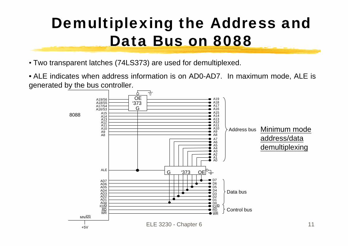
Demultiplexing the Address and Data Bus on 8088
• Two transparent latches (74LS373) are used for demultiplexed.
• ALE indicates when address information is on AD0-AD7. In maximum mode, ALE is generated by the bus controller.
Minimum mode address/data demultiplexing
G ‘373 OE
8088
A19/S6A18/S5A17/S4A16/S3
A15A14A13A12A11A10A9A8
ALE
MN/MX
+5V
RD
AD0
AD7AD6AD5AD4AD3AD2AD1
IO/M
WR
A13
A3
A19A18A17A16A15A14
A12A11A10A9
A6
A8A7
A5A4
A2A1A0
Address bus
D7D6D5D4D3D2D1D0
WRRDIO/M
Data bus
Control bus
OE‘373
G

ELE 3230 - Chapter 6 12
Latches
The address and data bus of the 8088 are multiplexed on pins AD0 to AD7. Address information are contained on AD0-AD7 only when ALE (address latch enable) is asserted.
External Latches are needed to store (“latch”) the addressing information before AD0-AD7 change to carrying data.
A latch simply consists of a D-type flip-flop with additional logic to select when to read and output data.
ELE 3230 - Chapter 6 13
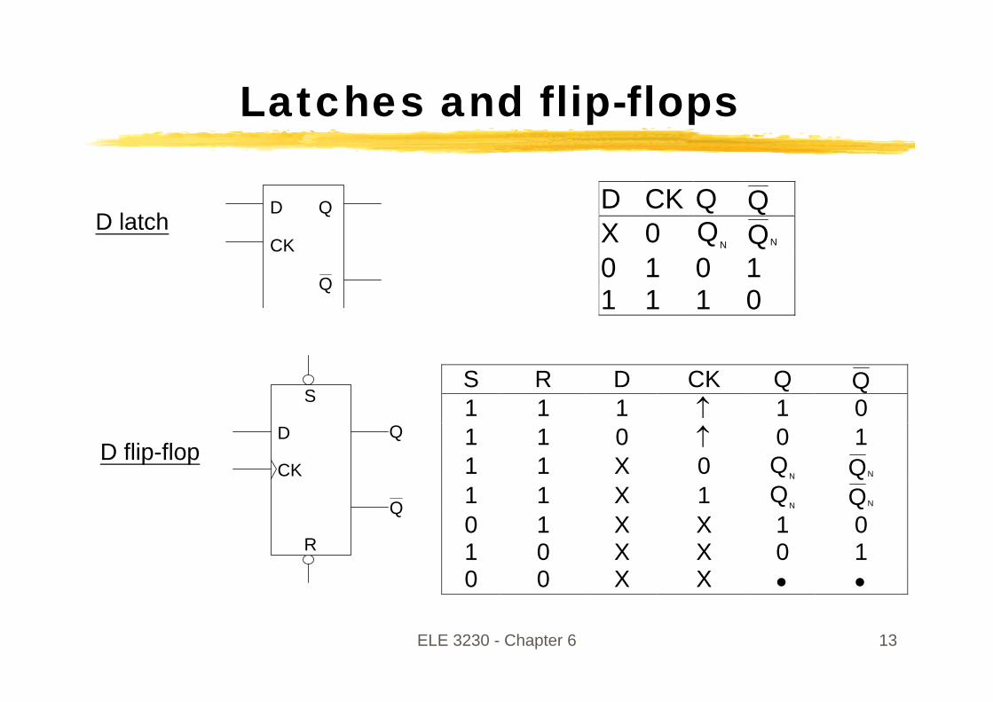
Latches and flip-flops
D CK Q QX 0 N
Q NQ0 1 0 11 1 1 0
S R D CK Q Q1 1 1 ↑ 1 01 1 0 ↑ 0 11 1 X 0 N
Q NQ1 1 X 1 N
Q NQ0 1 X X 1 01 0 X X 0 10 0 X X • •
D latch
D flip-flop
D Q
CK
Q
Q
Q
S
D
CK
R
ELE 3230 - Chapter 6 14
Latches(cont.)
Integrated circuits containing many latches (one latch is needed per bit) are available to perform the latching function of an address line e.g. 8282, 74LS373.
These packages typically have a single input, called “strobe”(STB), “latch enable” (LE) or “Gate” (G), which qualifies the data (i.e. passes the data to the flip-flops only when it the strobe or gate input is high).
Some latches also have an “output enable” (OE) input which qualifies the output data (when OE is low, the outputs are open circuit).
ELE 3230 - Chapter 6 15
8088 Fan-out and Buffers
In order to drive the system buses, which typically have many devices attached and with large capacitance, the address and data output pins must be buffered.
A buffer merely amplifies the output current.
Demultiplexed pins are already buffered by latches (e.g. 74LS373).
Un-multiplexed address pins can be buffered by 74LS245
octal bi-directional buffer and 74LS244 uni-directional buffer.
16
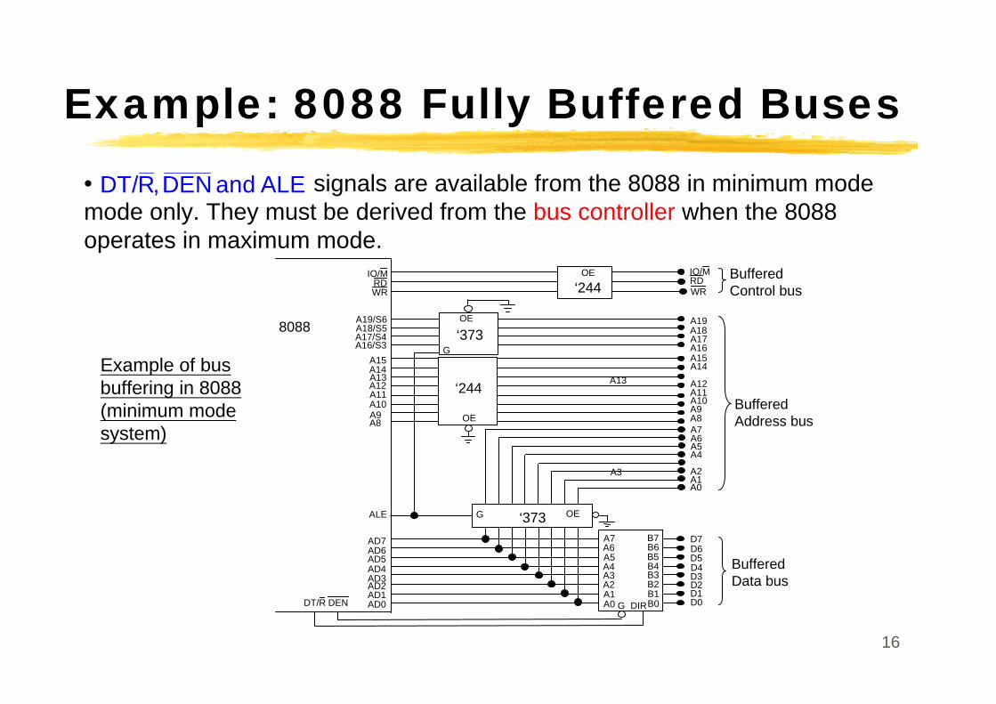
Example: 8088 Fully Buffered Buses
A13
A3
• signals are available from the 8088 in minimum mode mode only. They must be derived from the bus controller when the 8088 operates in maximum mode.
DT/R, DEN and ALE
Example of bus buffering in 8088 (minimum mode system)
OE
‘373G
A19A18A17A16A15A14
A12A11A10A9
A6
A8A7
A5A4
A2A1A0
Buffered Address bus
G ‘373 OE
WRRDIO/M Buffered
Control bus‘244
D7D6D5D4D3D2D1D0
Buffered Data bus
A7A6A5A4A3A2A1A0
B7B6B5B4B3B2B1B0
8088 A19/S6A18/S5A17/S4A16/S3
A15A14A13A12A11A10A9A8
ALE
AD4
AD0
AD7AD6AD5
AD3AD2AD1
RDIO/M
WR
DT/R DEN G DIR
‘244
OE
OE
17
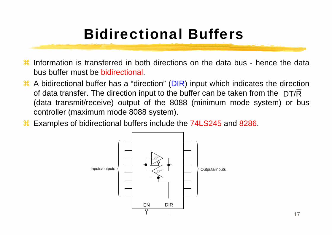
Bidirectional Buffers
Information is transferred in both directions on the data bus - hence the data bus buffer must be bidirectional.A bidirectional buffer has a “direction” (DIR) input which indicates the direction of data transfer. The direction input to the buffer can be taken from the(data transmit/receive) output of the 8088 (minimum mode system) or bus controller (maximum mode 8088 system).Examples of bidirectional buffers include the 74LS245 and 8286.
RDT/
DIREN
Outputs/inputsInputs/outputs
ELE 3230 - Chapter 6 18
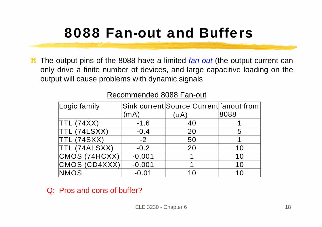
8088 Fan-out and Buffers
The output pins of the 8088 have a limited fan out (the output current can only drive a finite number of devices, and large capacitive loading on the output will cause problems with dynamic signals
Logic family Sink current(mA)
Source Current(µA)
fanout from8088
TTL (74XX) -1.6 40 1TTL (74LSXX) -0.4 20 5TTL (74SXX) -2 50 1TTL (74ALSXX) -0.2 20 10CMOS (74HCXX) -0.001 1 10CMOS (CD4XXX) -0.001 1 10NMOS -0.01 10 10
Recommended 8088 Fan-out
Q: Pros and cons of buffer?
19
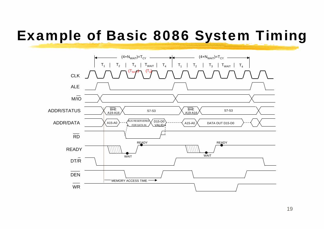
Example of Basic 8086 System Timing
MEMORY ACCESS TIME
T1 T2 T3 TWAIT T4 T1 T2 T3 TWAIT T4
(4+NWAIT)=TCY (4+NWAIT)=TCY
CLK
ALE
M/IO
S7-S3A19-A16BHE
A19-A16BHE S7-S3ADDR/STATUS
WAIT
READY
WAIT
READY
READY
BUS RESERVERED
FOR DATA INA15-A0 D15-D0
VALID A15-A0 DATA OUT D15-D0
RD
ADDR/DATA
DT/R
DEN
WR
(TWAIT) (T3)
ELE 3230 - Chapter 6 20
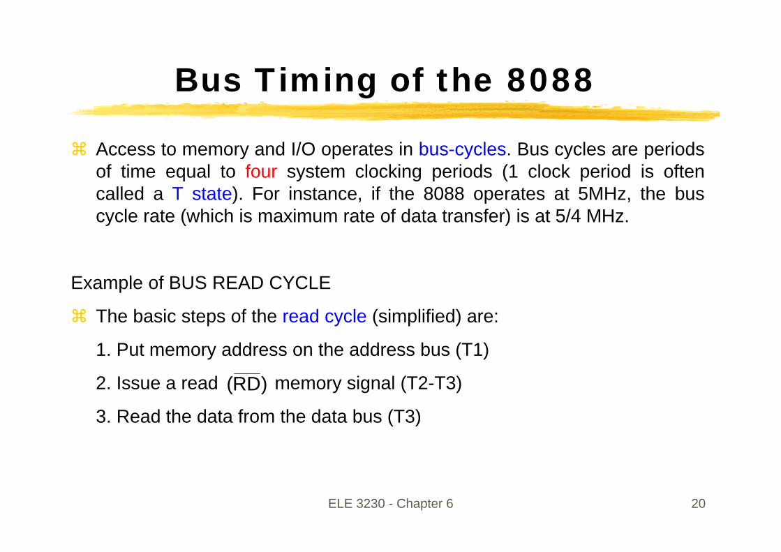
Bus Timing of the 8088
Access to memory and I/O operates in bus-cycles. Bus cycles are periods of time equal to four system clocking periods (1 clock period is often called a T state). For instance, if the 8088 operates at 5MHz, the bus cycle rate (which is maximum rate of data transfer) is at 5/4 MHz.
Example of BUS READ CYCLE
The basic steps of the read cycle (simplified) are:
1. Put memory address on the address bus (T1)
2. Issue a read memory signal (T2-T3)
3. Read the data from the data bus (T3)
)RD(
ELE 3230 - Chapter 6 21
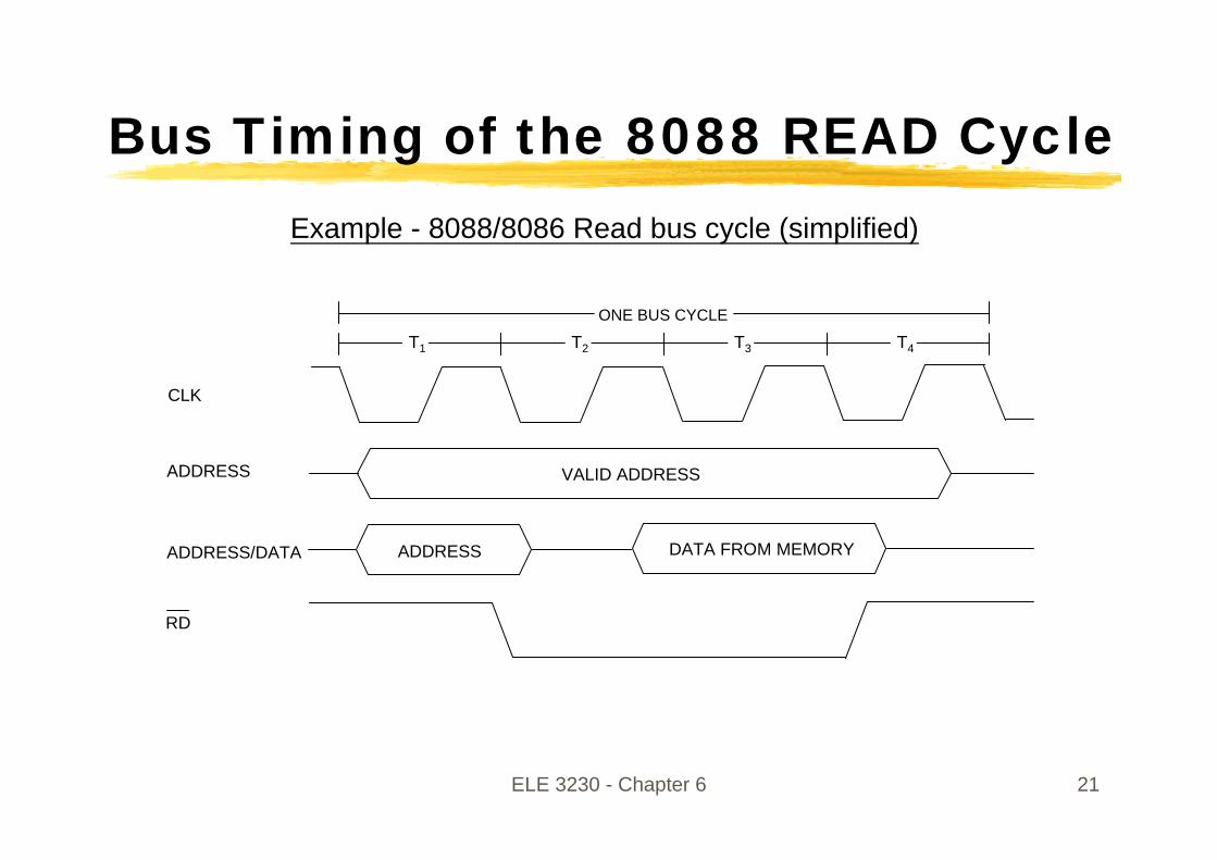
Bus Timing of the 8088 READ CycleExample - 8088/8086 Read bus cycle (simplified)
VALID ADDRESS
ONE BUS CYCLE
T1 T2 T3 T4
ADDRESS DATA FROM MEMORY
CLK
ADDRESS
ADDRESS/DATA
RD
ELE 3230 - Chapter 6 22
Bus Timing Diagrams (General)
To transfer data without error on the system bus, the signals in the bus must change and hold the values within a certain period of time in a bus cycle.
Physically, a system bus consists of conducting wires or tracks on circuit board. These have distributed inductance and capacitance which tend to distort the signal waveforms.
Long system buses can have clock skew (there is a delay in signals received by distant peripherals - and their clock is slightly out of phase with the clock received by the microprocessor).
The rise-time, fall-time, and duration of signals must be within the specifications of the device or microprocessor - otherwise errors will occur in transferring data. The manufacturer’s data sheet contain important information on the timing requirements which can be quite demanding.
ELE 3230 - Chapter 6 23
Bus Cycle Operation
T1 - start of bus cycle. Actions include setting control signals (or S0-S2 status lines) to give the required values for ALE, and , and putting a valid address onto the address bus.
RDT/ IO/M
T2 - the or control signals are issued, is asserted and in the case of a write, data is put onto the data bus. The turns on the data bus buffers to connect the cpu to the external data bus. The READY input to the cpu is sampled at the end of T2 and if READY is low, a wait state TW (one or more) is inserted before T3 begins.
WRRD DENDEN
ELE 3230 - Chapter 6 24
Bus Cycle Operation
T3 - this clock period is provided to allow memory to access the data. If the bus cycle is a read cycle, the data bus is sampled at the end of T3.
T4 - all bus signals are deactivated in preparation for the next clock cycle. The 8088 also finishes sampling the data (in a read cycle) in this period. For the write cycle, the trailing edge of the signal transfers data to the memory or I/O, which activates and writes when
returns to logic 1 level.
WR
WR
ELE 3230 - Chapter 6 25
Read Cycle Timing
The most important information contained in the read timing diagram is the amount of the time allowed for getting data from memory.
Memory chips usually have a specified memory access time.
The memory access time is defined as the interval from when a valid address is put on the address bus (near the start of T1) to the time when the data is read (near the end of T3). The permitted memory access time is therefore less than three T states if no wait states are added.
To find the exact access time permitted by the read timing diagram:1. Find the maximum interval necessary for a valid address to appear after the start
of T1. This interval is given the symbol TCLAV (clock-to-address valid) the microprocessor data sheet (For a 5MHz 8088, TCLAV=110ns)
ELE 3230 - Chapter 6 26
Read Cycle Timing (cont.)
2. Valid data must appear on the data bus before the end of T3 in order to allow the data to be read. The minimum time interval before the end of T3 for valid data to appear is given the symbol TDVCL (data valid-to clock) and is specified as 30ns for the 5MHz 8088.
3. The maximum memory access time=3T-TCLAV-TDVCL which, for the 5MHz 8088, is 600-110-30=460 (ns). Actually the memory access time must be less than this since there will be propagation delays in going through buffers (about another 40ns).
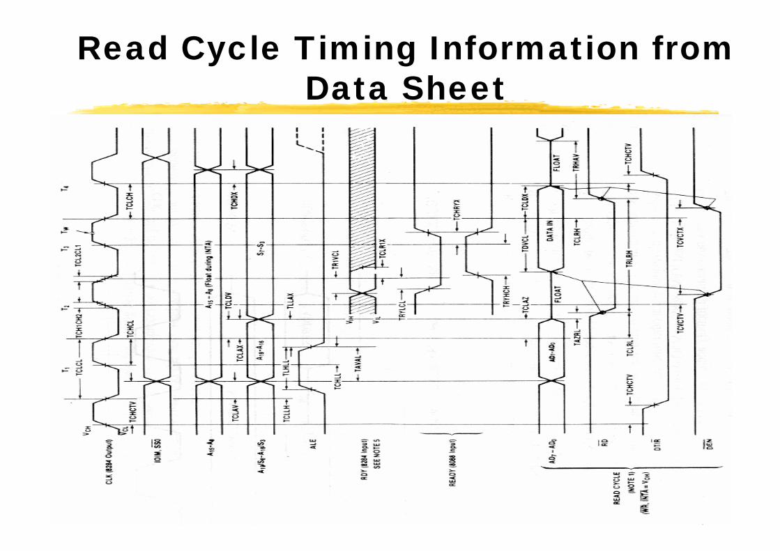
Read Cycle Timing Information from Data Sheet
ELE 3230 - Chapter 6 28
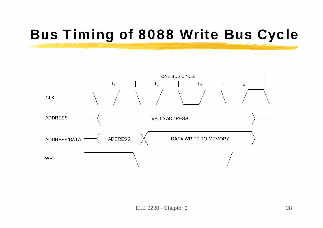
Bus Timing of 8088 Write Bus Cycle
VALID ADDRESS
ONE BUS CYCLE
T1 T2 T3 T4
ADDRESS DATA WRITE TO MEMORY
CLK
ADDRESS
ADDRESS/DATA
WR
ELE 3230 - Chapter 6 29
Write bus cycle (simplified) consists of :1. Put memory address on the address bus (T1)2. Issue a write to memory signal (T2-T3)3. Send data to data bus (T2-T3) and write to memory
Actual (non-simplified) read and write bus cycle include changes on other signals such as M/IO, ALE, DEN, DT/R and READY. The actual cycles will be investigated in detail later.
T4 in the bus cycle is used to deactivate all the signals in preparation for the next bus cycle.
Example - 8088/8086 Write Bus Cycle (simplified)
)(WR
ELE 3230 - Chapter 6 30
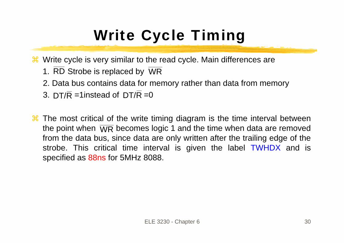
Write Cycle TimingWrite cycle is very similar to the read cycle. Main differences are 1. Strobe is replaced by2. Data bus contains data for memory rather than data from memory3. =1instead of =0
The most critical of the write timing diagram is the time interval between the point when becomes logic 1 and the time when data are removed from the data bus, since data are only written after the trailing edge of the strobe. This critical time interval is given the label TWHDX and is specified as 88ns for 5MHz 8088.
RD WR
RDT/ RDT/
WR
ELE 3230 - Chapter 6 31
Write Cycle Timing
TW
TCLAX
T1 T2 T3 T4
VCH
VCL
CLK(8284 Output)
AD7-AD0
DEN
WR
WRITE CYCLE NOTE 1
TCH1CH2 TCL2CL1
TCLAVTCLDV TCHDX
TCVCTV AD0TCVCTV
TCVCTV
TWLWH
TCVCTX
TWHDX
AD7-AD0 DATA OUT
ELE 3230 - Chapter 6 32
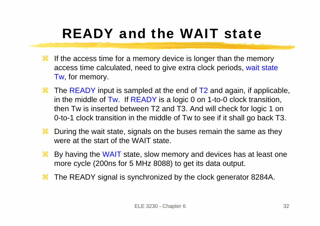
READY and the WAIT stateIf the access time for a memory device is longer than the memoryaccess time calculated, need to give extra clock periods, wait stateTw, for memory.
The READY input is sampled at the end of T2 and again, if applicable, in the middle of Tw. If READY is a logic 0 on 1-to-0 clock transition, then Tw is inserted between T2 and T3. And will check for logic 1 on 0-to-1 clock transition in the middle of Tw to see if it shall go back T3.
During the wait state, signals on the buses remain the same as they were at the start of the WAIT state.
By having the WAIT state, slow memory and devices has at least one more cycle (200ns for 5 MHz 8088) to get its data output.
The READY signal is synchronized by the clock generator 8284A.
ELE 3230 - Chapter 6 33
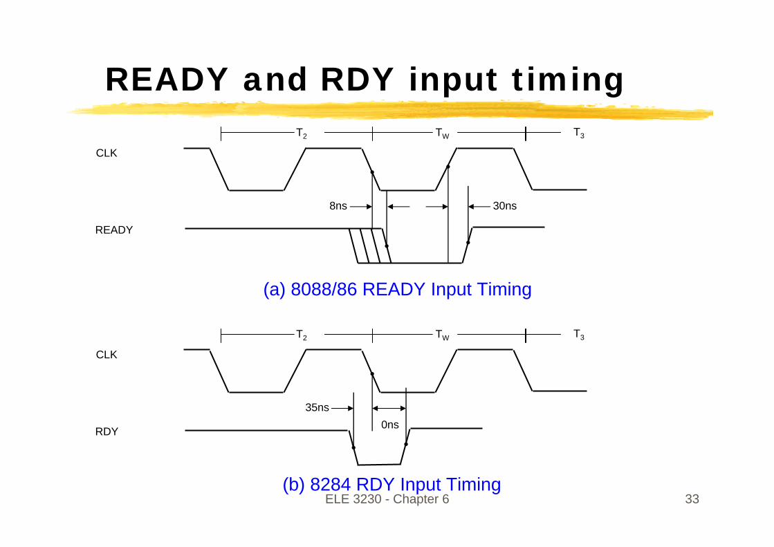
READY and RDY input timing
CLK
READY
T2 TW T3
8ns 30ns
CLK
RDY
T2 TW T3
35ns0ns
(b) 8284 RDY Input Timing
(a) 8088/86 READY Input Timing
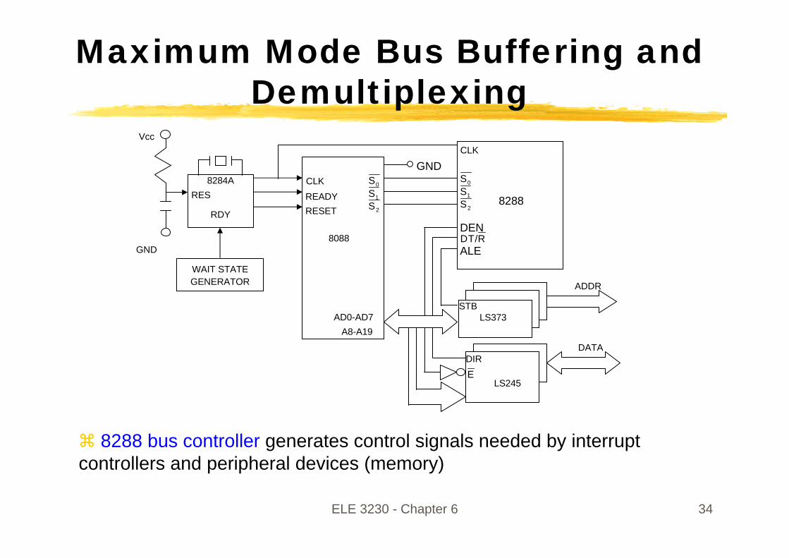
ELE 3230 - Chapter 6 34
Maximum Mode Bus Buffering and Demultiplexing
8288 bus controller generates control signals needed by interrupt controllers and peripheral devices (memory)
8284A
RDY
CLK READY RESET
8088
AD0-AD7A8-A19
CLK
8288
STBLS373
DIR
LS245
WAIT STATEGENERATOR
RES
GND0S1S2S
0S1S2S
DEN
ALEDT/R
E
GND
Vcc
ADDR
DATA
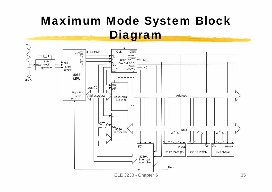
ELE 3230 - Chapter 6 35
Vcc
NC
GND
GND
Address/data Address
Data
IR0-7
MXMN/
0S
1SCLK 2SREADYRESET
8088MPU
70 ADAD −
198 AA −INTR
T
OE8286
Transceiver
EN
8259AInterruptcontroller
INT
STB
OE
8282 Latch(1, 2 or 3)
WEOE
2142 RAM (2)
OE
27162 PROM
CS WRRD
Peripheral
8284ARES clock
generator
CLK MRDC
0S MWTC
1S AMWC2S IORC
DEN IOWCRDT/ IOWCA
ALE INTA
Maximum Mode System Block Diagram
GND
NC
8288Bus Ctrl
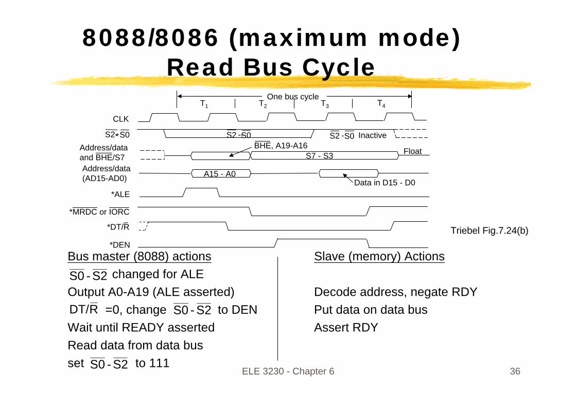
ELE 3230 - Chapter 6 36
Bus master (8088) actions Slave (memory) Actionschanged for ALE
Output A0-A19 (ALE asserted) Decode address, negate RDY=0, change to DEN Put data on data bus
Wait until READY asserted Assert RDYRead data from data busset to 111
8088/8086 (maximum mode) Read Bus Cycle
RDT/
S2-S0
S2-S0
One bus cycle
CLK
S2- S0* S2 S0-- S2 S0- InactiveAddress/data and BHE/S7
BHE, A19-A16S7 - S3 Float
Address/data (AD15-AD0) A15 - A0
Data in D15 - D0*ALE
*MRDC or IORC
*DT/R
*DEN
T1 T4T3T2
Triebel Fig.7.24(b)
S2-S0
ELE 3230 - Chapter 6 37
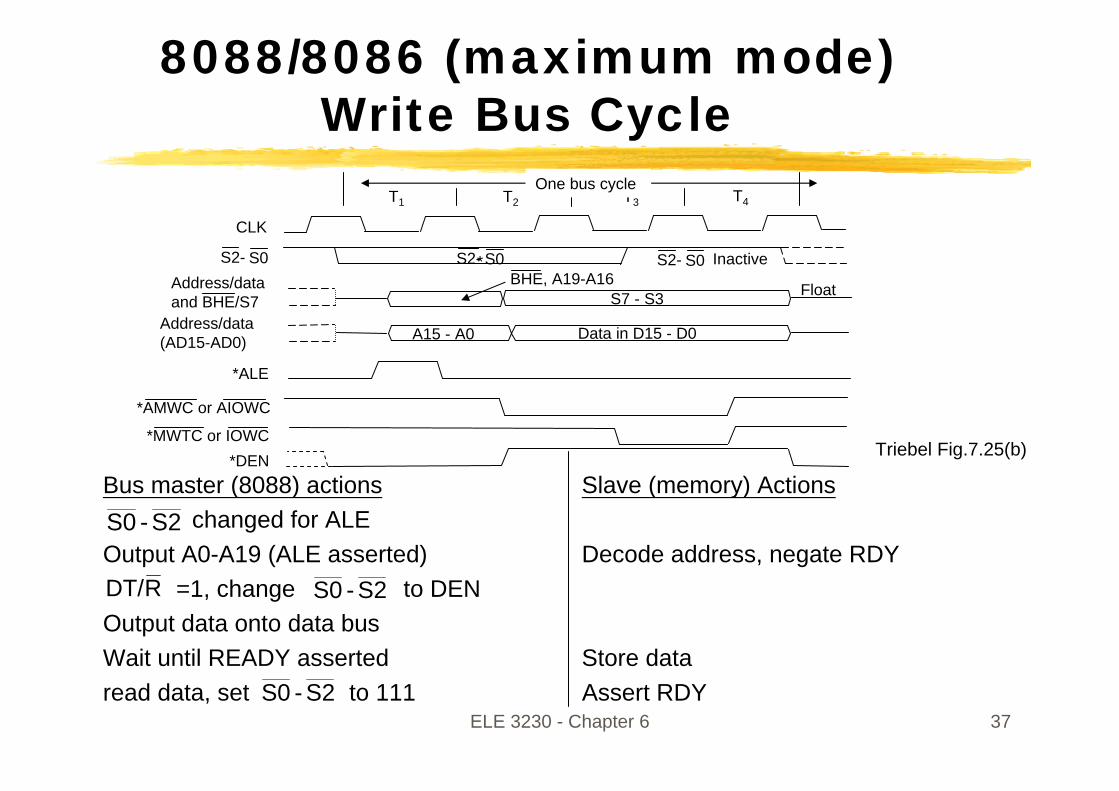
8088/8086 (maximum mode) Write Bus Cycle
Address/data (AD15-AD0)
T1 T4T3T2One bus cycle
CLK
S2- S0 S2- S0* S2- S0 InactiveAddress/data and BHE/S7
BHE, A19-A16S7 - S3 Float
*ALE
*AMWC or AIOWC
A15 - A0 Data in D15 - D0
*MWTC or IOWC*DEN
Triebel Fig.7.25(b)
Bus master (8088) actions Slave (memory) Actionschanged for ALE
Output A0-A19 (ALE asserted) Decode address, negate RDY=1, change to DEN
Output data onto data busWait until READY asserted Store dataread data, set to 111 Assert RDY
RDT/ S2-S0
S2-S0
S2-S0


![8203 3200-3230 Fastrac Spec (UK) - RS Duncan Plant Hire5]JCB... · Pipework/hose: BSP standard. Standard Plus Auxiliary Hydraulic Package 3200 3230 3200 3230 ... JCB FASTRAC | 3200/3230](https://img.pdfslide.us/doc/110x75/5e9f5b91316bde65821be733/8203-3200-3230-fastrac-spec-uk-rs-duncan-plant-5jcb-pipeworkhose-bsp.jpg)