Embed Size (px)
Citation preview
CENG 5534 Advanced Digital System Design Summer 2016
Final Project Due Date: July 26
You have designed and validated various components in VHDL throughout the semester using Xilinx ISE. In your final VHDL project, you are to design a simple CPU using previously designed components as well as a few new ones. You should email your project (VHDL code and report) to TA by 1pm, Tuesday, July 26. In addition, the hardcopy of your report should be submitted on the same day in class. Your submission is not complete until we receive both your typed report and your source codes as an email attachment. Late submissions will get 0. In your report, you need to add necessary comments in each VHDL code (including design and testbench) and provide explanations on the waveforms.
NOTE: You are allowed to work in groups of two for this project and submit single report. Both students will receive the same grade.
Code Submission Guidelines: o Each problem in a homework is a Xilinx workspace folder o Name each program with a decent name (e.g., project_Inst_regist.vhd, etc.) o Zip all workspace folders in one zip folder o Name the zip file in the following format: ceng5534_project_yourlastname.zip (e.g.,
ceng5534_project_koc.zip) o Subject of the email should contain “ceng5534-project” o Email the zip file to TA
Project Description: (100 pts) You are to design a simple CPU that would allow you to perform the following operations:
1. Load Instructions into your Instruction memory. 2. Load a value into register A. (Ld A) 3. Load a value into register B. (Ld B) 4. Perform any logical operation using the ALU (16-bit operations) and store the result in
register C. 5. Store the value of register C back to memory. (Store C) 6. Read the data stored in data memory at the given Address. (RdMem) 7. Exit the program without further execution. (Exit)
All the instructions must be stored in memory before the execution starts. Your CPU will access the memory to fetch the instructions and execute them one after the other.
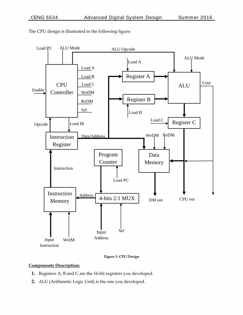
CENG 5534 Advanced Digital System Design Summer 2016
The CPU design is illustrated in the following figure:
Figure 1: CPU Design
Components Description:
1. Registers A, B and C are the 16-bit registers you developed.
2. ALU (Arithmetic Logic Unit) is the one you developed.
CPU Controller
Register A
Register B
Register C
Instruction Register
Instruction Memory
Program Counter
Data Memory
ALU
4-bits 2:1 MUX
WeIM Input
Address Sel
DM out CPU out
Cout
ALU Mode
Load C Load B
Load A Load A
Load B Load C
WeDM
ReDM
Sel
Opcode Load IR
Data/Address
Instruction
Address
Load PC ALU Mode ALU Opcode
WeDM ReDM
Load PC
Enable
Input Instruction
CENG 5534 Advanced Digital System Design Summer 2016
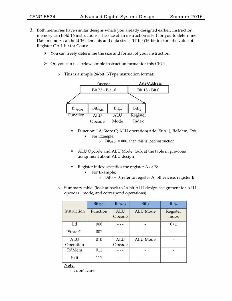
3. Both memories have similar designs which you already designed earlier. Instruction memory can hold 16 instructions. The size of an instruction is left for you to determine. Data memory can hold 16 elements and data size is 17-bit (16-bit to store the value of Register C + 1-bit for Cout):
You can freely determine the size and format of your instruction.
Or, you can use below simple instruction format for this CPU:
o This is a simple 24-bit I-Type instruction format:
Function: Ld; Store C; ALU operation(Add, Sub,..); RdMem; Exit
• For Example: o Bit23-21 = 000, then this is load instruction.
ALU Opcode and ALU Mode: look at the table in previous
assignment about ALU design
Register index: specifies the register A or B: • For Example:
o Bit16 = 0: refer to register A; otherwise, register B
o Summary table: (look at back to 16-bit ALU design assignment for ALU opcodes , mode, and correspond operations)
Instruction
Bit23-21 Bit20-18 Bit17 Bit16
Function ALU Opcode
ALU Mode Register Index
Ld 000 - - - - 0/1
Store C 001 - - - - -
ALU Operation
010 ALU Opcode
ALU Mode -
RdMem 011 - - - - -
Exit 111 - - - - -
Note: - : don’t care
Register Index
ALU Mode
ALU Opcode
Function
Data/Address Opcode Bit 23 - Bit 16 Bit 15 - Bit 0
Bit23-21 Bit20-18 Bit17 Bit16
CENG 5534 Advanced Digital System Design Summer 2016
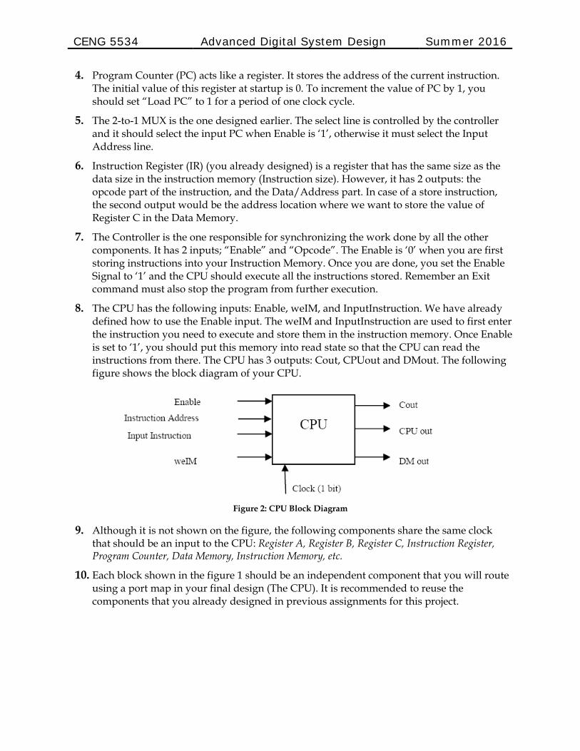
4. Program Counter (PC) acts like a register. It stores the address of the current instruction. The initial value of this register at startup is 0. To increment the value of PC by 1, you should set “Load PC” to 1 for a period of one clock cycle.
5. The 2-to-1 MUX is the one designed earlier. The select line is controlled by the controller and it should select the input PC when Enable is ‘1’, otherwise it must select the Input Address line.
6. Instruction Register (IR) (you already designed) is a register that has the same size as the data size in the instruction memory (Instruction size). However, it has 2 outputs: the opcode part of the instruction, and the Data/Address part. In case of a store instruction, the second output would be the address location where we want to store the value of Register C in the Data Memory.
7. The Controller is the one responsible for synchronizing the work done by all the other components. It has 2 inputs; “Enable” and “Opcode”. The Enable is ‘0’ when you are first storing instructions into your Instruction Memory. Once you are done, you set the Enable Signal to ‘1’ and the CPU should execute all the instructions stored. Remember an Exit command must also stop the program from further execution.
8. The CPU has the following inputs: Enable, weIM, and InputInstruction. We have already defined how to use the Enable input. The weIM and InputInstruction are used to first enter the instruction you need to execute and store them in the instruction memory. Once Enable is set to ‘1’, you should put this memory into read state so that the CPU can read the instructions from there. The CPU has 3 outputs: Cout, CPUout and DMout. The following figure shows the block diagram of your CPU.
Figure 2: CPU Block Diagram
9. Although it is not shown on the figure, the following components share the same clock that should be an input to the CPU: Register A, Register B, Register C, Instruction Register, Program Counter, Data Memory, Instruction Memory, etc.
10. Each block shown in the figure 1 should be an independent component that you will route using a port map in your final design (The CPU). It is recommended to reuse the components that you already designed in previous assignments for this project.
CENG 5534 Advanced Digital System Design Summer 2016
A sample set of instructions:
Remember, you have to set Enable to ‘0’ in order to set these instructions. They must NOT be hardcoded into your memory. They should be fed to your CPU using your test bench.
1. Ld A 0x0003
2. Ld B 0x0006
3. ADD 0x0000 (0x0000 is stored with the instruction when no value is needed)
4. Store C 0x0001 (Store value of the addition to location 0x0001 of data memory)
5. AND 0x0000
6. Store C 0x0002
7. RdMem 0x0001
8. Ld B 0x000B
9. Mult AB 0x0000 (Remember, only the 8 LSB of A and B are multiplied)
10. Store C 0x0003
11. RdMem 0x0003
12. Exit 0x0000
13. RdMem 0x0000 (Should not happen).
Your testbench must include a “good” set of instructions that would test the functionality of your CPU. Any missing particular case would make you lose points. The testbench is what determines if your design is working or not. So, make sure you think well about how to design one.
In your report, make sure to include the VHDL codes of the newly designed components along with their testbenches and the commented waveforms. That is, provide the latter for the following components:
Program Counter
Instruction Register
Data Memory
Instruction Memory
CPU controller
CPU design
CENG 5534 Advanced Digital System Design Summer 2016
Grading Guidelines:
1. Program Counter (8 pt)
Code (4 pt)
Waveform (3 pt)
Explain (1 pt)
2. Instruction Register (8 pt)
Code (4 pt)
Waveform (3 pt)
Explain (1 pt)
3. Data Memory (8 pt)
Code (4 pt)
Waveform (3 pt)
Explain (1 pt)
4. Instruction Memory (8 pt)
Code (4 pt)
Waveform (3 pt)
Explain (1 pt)
5. Controller (18 pt)
Code (8 pt)
Waveform (6 pt)
Explain (4 pt)
6. CPU Design (40 pt)
Code (10 pt)
Waveform (20 pt)
Explain (10 pt)
7. Report Overall (10 pt)
--------------------------------------------- Total: 100pts