Embed Size (px)
Citation preview
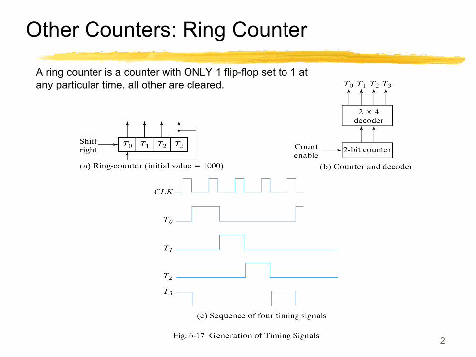
2
Other Counters: Ring Counter
A ring counter is a counter with ONLY 1 flip-flop set to 1 at any particular time, all other are cleared.
3
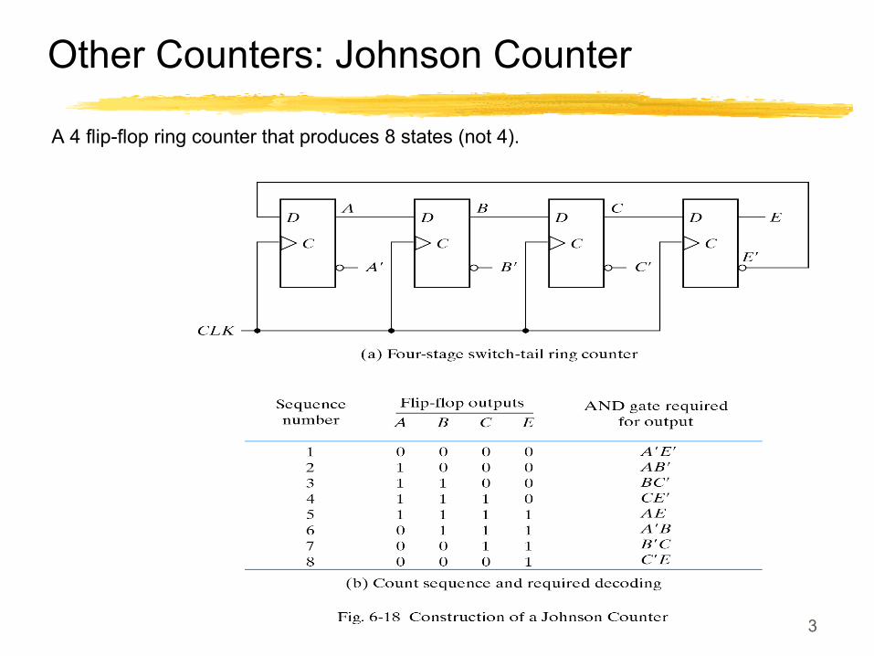
Other Counters: Johnson Counter
A 4 flip-flop ring counter that produces 8 states (not 4).
4
Memory
Memory unit: Stores binary information A collection of cells
Two types of memory: RAM-Random Access Memory ROM-Read Only Memory
RAM: Can read and write ROM:Programmable Logic Device (PLD)
5
Programmable Logic Device: PLD
Programming: hardware procedure to insert bits into the configuration.
Different PLDs: ROM, Program Logic Array (PLA), Program Array Logic (PAL), Field Programmable Field Array (FPGA)
PLD may include hundreds of millions of gates
To show logic we use concise forms
6
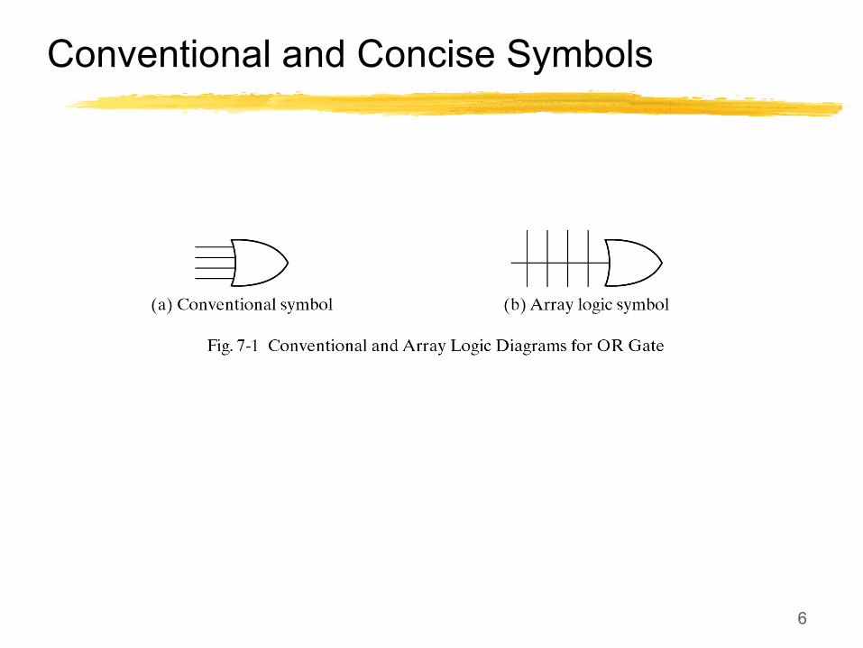
Conventional and Concise Symbols
7
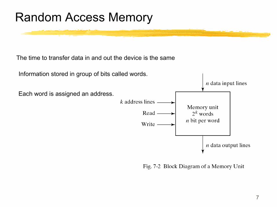
Random Access Memory
The time to transfer data in and out the device is the same
Information stored in group of bits called words.
Each word is assigned an address.
8
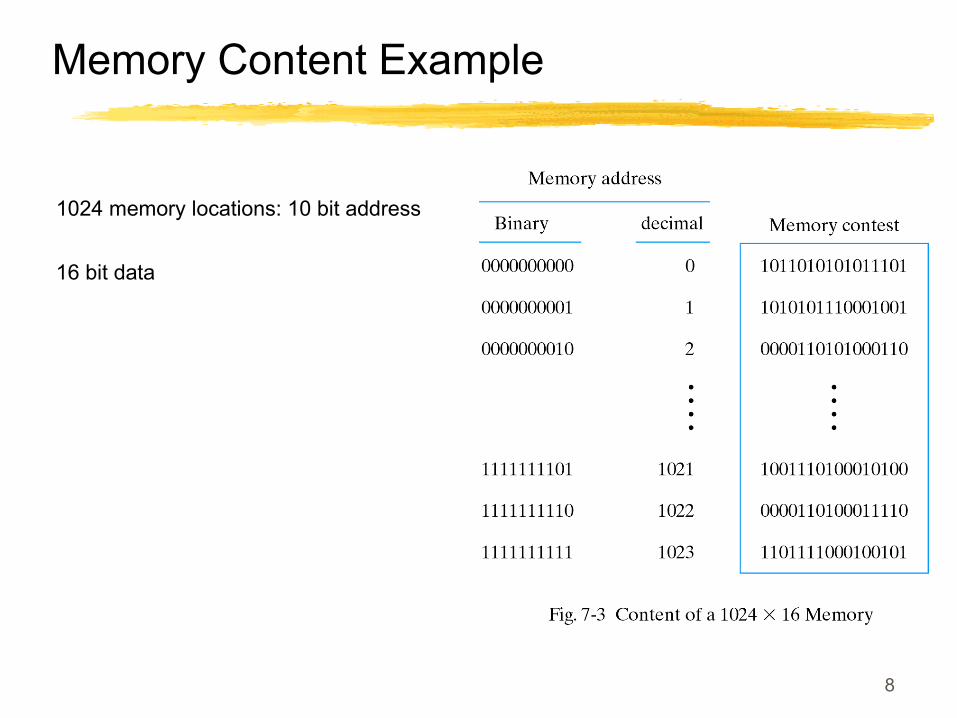
Memory Content Example
1024 memory locations: 10 bit address
16 bit data
9
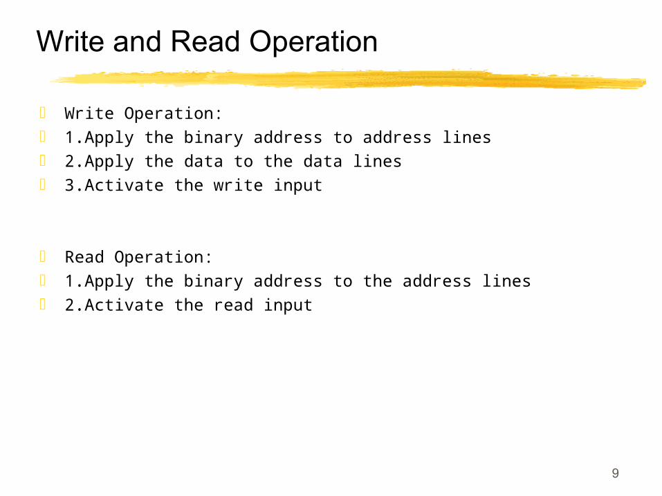
Write and Read Operation
Write Operation: 1.Apply the binary address to address lines 2.Apply the data to the data lines 3.Activate the write input
Read Operation: 1.Apply the binary address to the address lines 2.Activate the read input
10
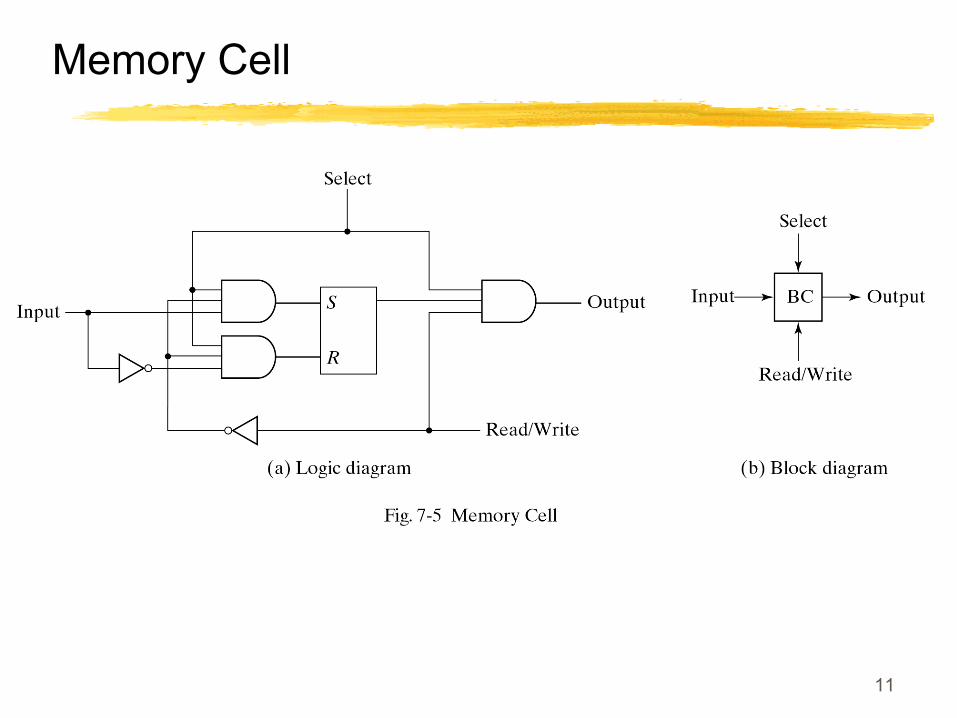
Memory Decoding
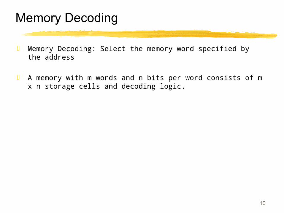
Memory Decoding: Select the memory word specified by the address
A memory with m words and n bits per word consists of m x n storage cells and decoding logic.
11
Memory Cell
12
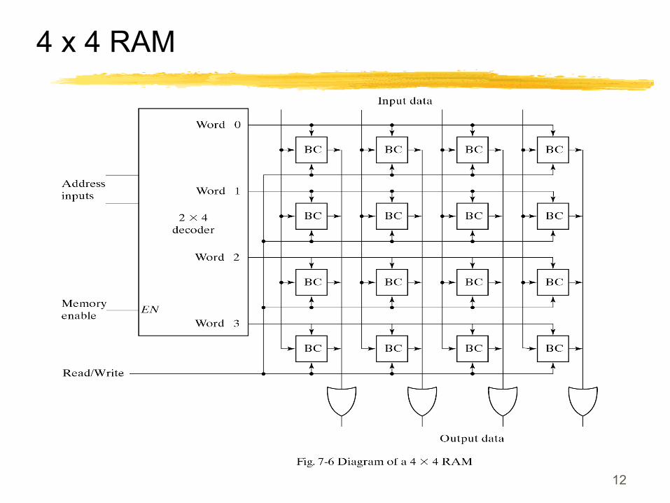
4 x 4 RAM
13
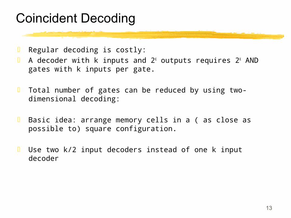
Coincident Decoding
Regular decoding is costly: A decoder with k inputs and 2K outputs requires 2K AND
gates with k inputs per gate.
Total number of gates can be reduced by using two-dimensional decoding:
Basic idea: arrange memory cells in a ( as close as possible to) square configuration.
Use two k/2 input decoders instead of one k input decoder
14
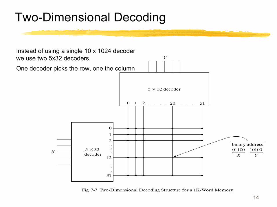
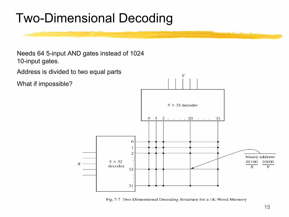
Two-Dimensional Decoding
Instead of using a single 10 x 1024 decoderwe use two 5x32 decoders.
One decoder picks the row, one the column
15
Two-Dimensional Decoding
Needs 64 5-input AND gates instead of 102410-input gates.
Address is divided to two equal parts
What if impossible?
16
Address Multiplexing
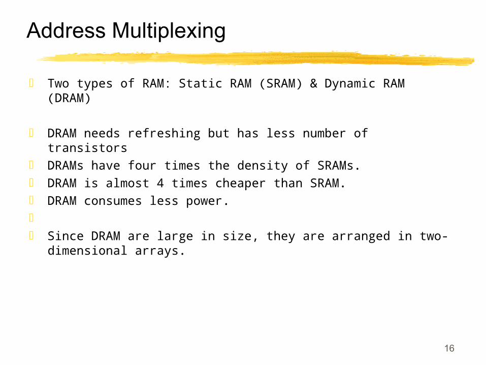
Two types of RAM: Static RAM (SRAM) & Dynamic RAM (DRAM)
DRAM needs refreshing but has less number of transistors
DRAMs have four times the density of SRAMs. DRAM is almost 4 times cheaper than SRAM. DRAM consumes less power. Since DRAM are large in size, they are arranged in two-
dimensional arrays.
17
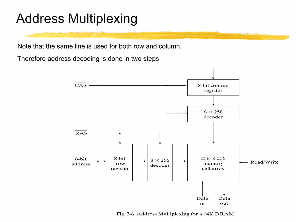
Address Multiplexing
Note that the same line is used for both row and column.
Therefore address decoding is done in two steps
18
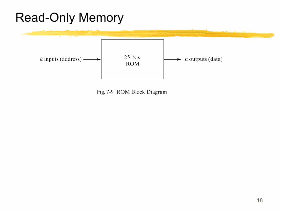
Read-Only Memory
19
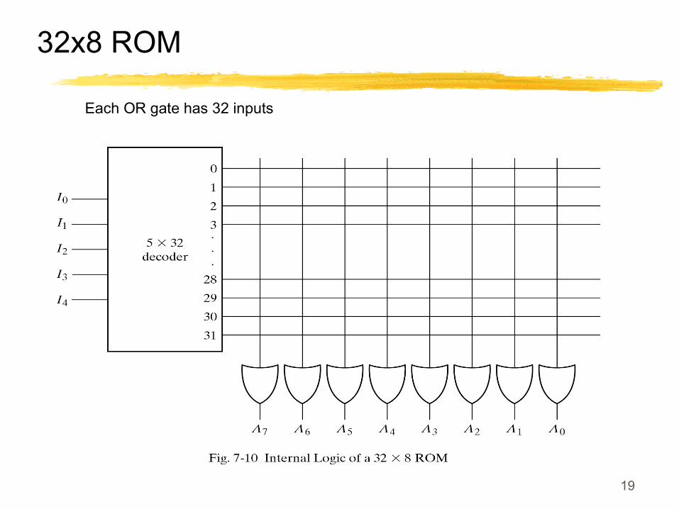
32x8 ROM
Each OR gate has 32 inputs
20
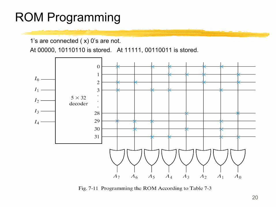
ROM Programming
At 00000, 10110110 is stored. At 11111, 00110011 is stored.
1’s are connected ( x) 0’s are not.
21
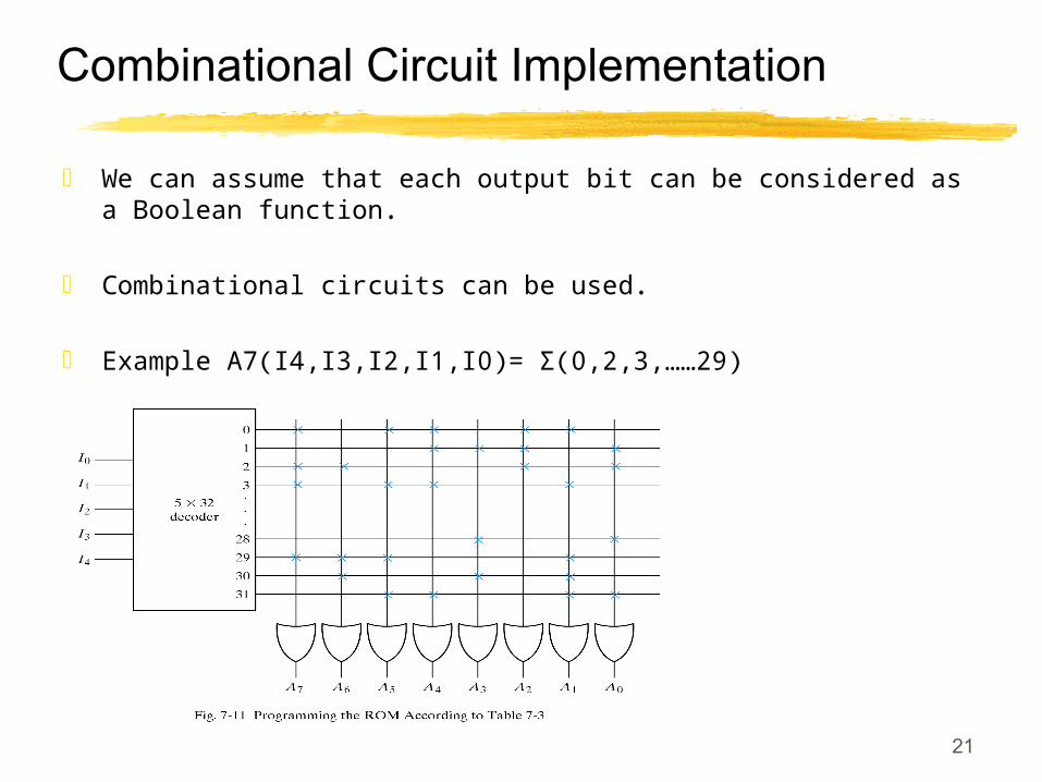
Combinational Circuit Implementation
We can assume that each output bit can be considered as a Boolean function.
Combinational circuits can be used.
Example A7(I4,I3,I2,I1,I0)= Σ(0,2,3,……29)
22
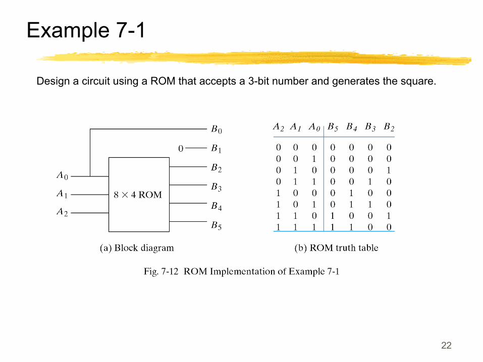
Example 7-1
Design a circuit using a ROM that accepts a 3-bit number and generates the square.
23
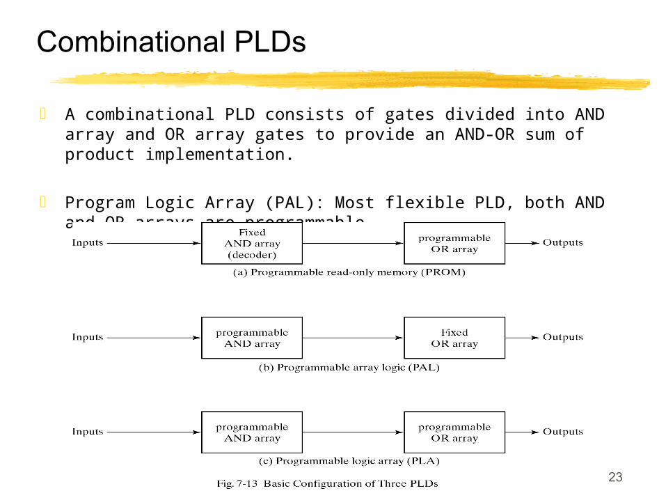
Combinational PLDs
A combinational PLD consists of gates divided into AND array and OR array gates to provide an AND-OR sum of product implementation.
Program Logic Array (PAL): Most flexible PLD, both AND and OR arrays are programmable
24
Programmable Logic Array
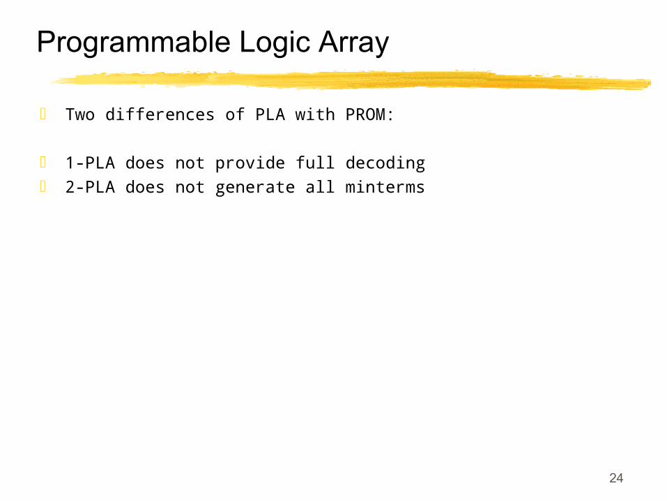
Two differences of PLA with PROM:
1-PLA does not provide full decoding 2-PLA does not generate all minterms
25
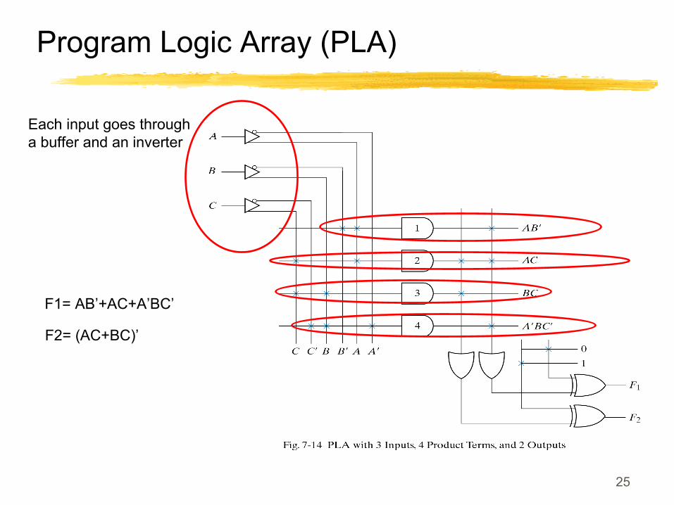
Program Logic Array (PLA)
Each input goes through a buffer and an inverter
F1= AB’+AC+A’BC’
F2= (AC+BC)’
26
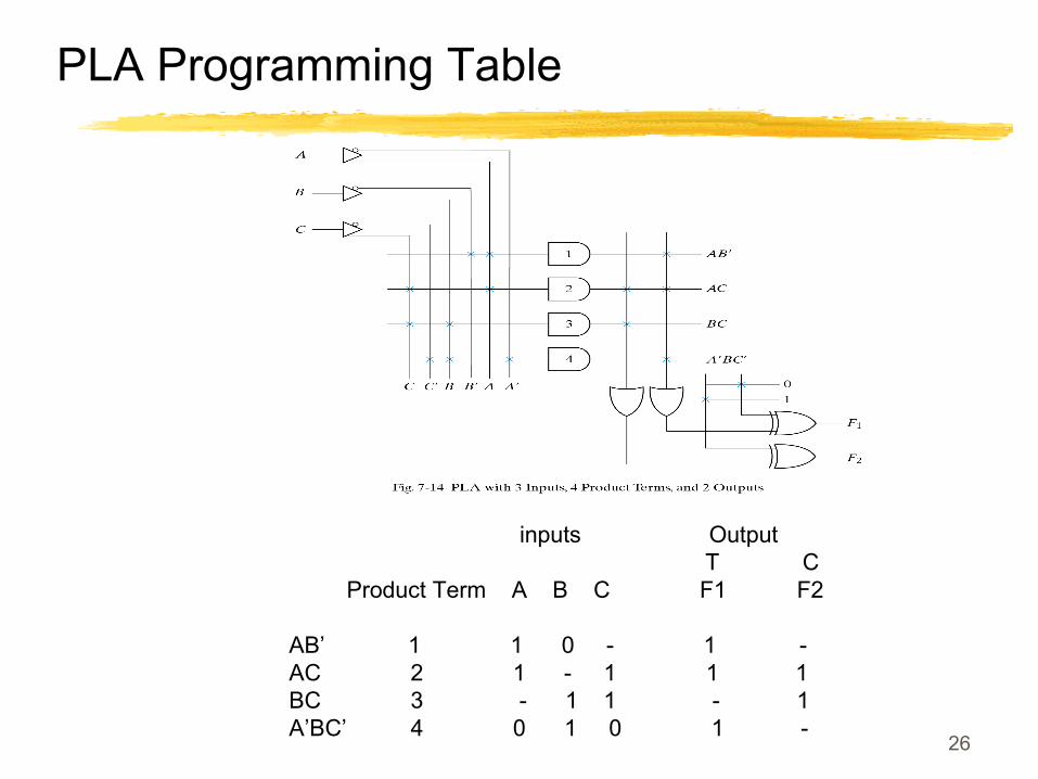
PLA Programming Table
inputs Output T C Product Term A B C F1 F2
AB’ 1 1 0 - 1 -AC 2 1 - 1 1 1BC 3 - 1 1 - 1 A’BC’ 4 0 1 0 1 -
27
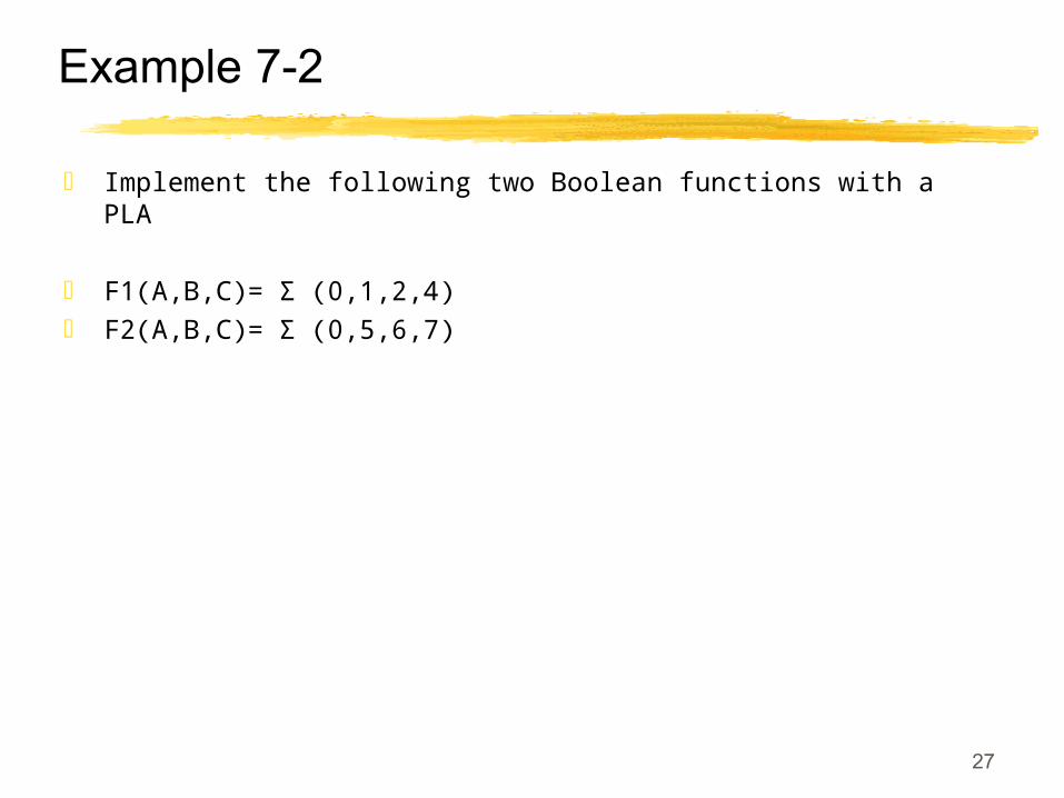
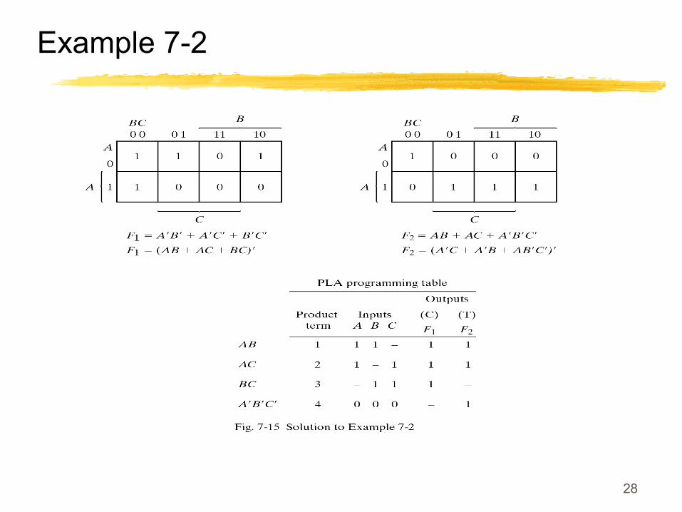
Example 7-2
Implement the following two Boolean functions with a PLA
F1(A,B,C)= Σ (0,1,2,4) F2(A,B,C)= Σ (0,5,6,7)
28
Example 7-2
29
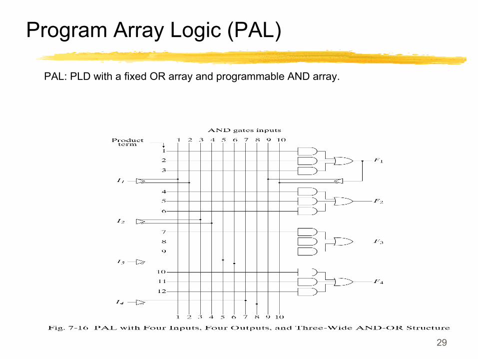
Program Array Logic (PAL)
PAL: PLD with a fixed OR array and programmable AND array.
30
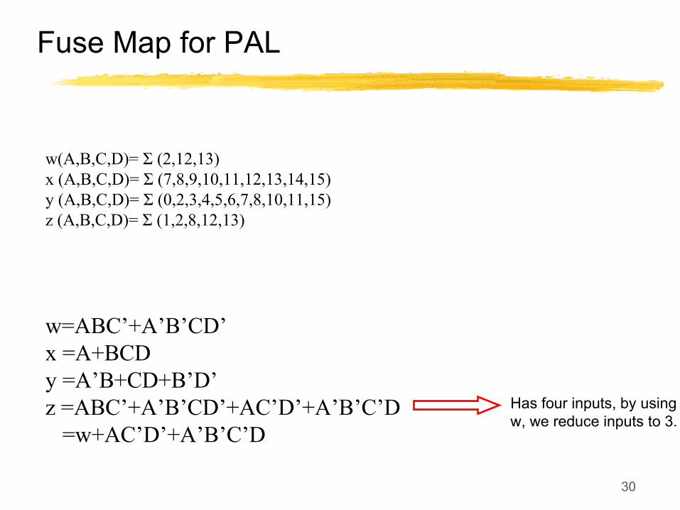
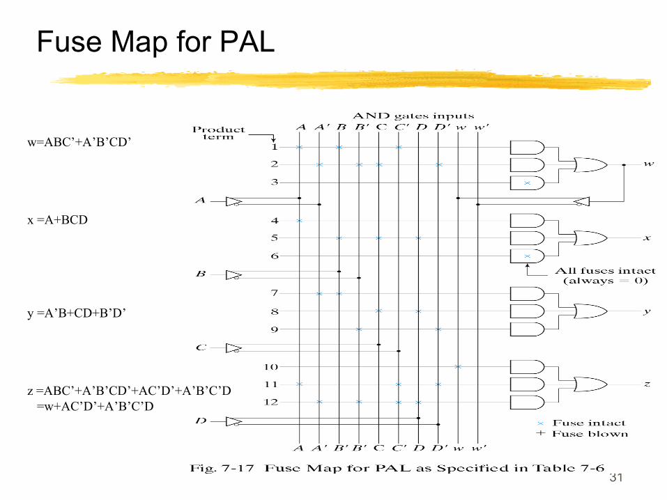
Fuse Map for PAL
w(A,B,C,D)= Σ (2,12,13)x (A,B,C,D)= Σ (7,8,9,10,11,12,13,14,15)y (A,B,C,D)= Σ (0,2,3,4,5,6,7,8,10,11,15)z (A,B,C,D)= Σ (1,2,8,12,13)
w=ABC’+A’B’CD’x =A+BCDy =A’B+CD+B’D’z =ABC’+A’B’CD’+AC’D’+A’B’C’D =w+AC’D’+A’B’C’D
Has four inputs, by usingw, we reduce inputs to 3.
31
Fuse Map for PAL
w=ABC’+A’B’CD’
x =A+BCD
y =A’B+CD+B’D’
z =ABC’+A’B’CD’+AC’D’+A’B’C’D =w+AC’D’+A’B’C’D
32
2003 final exam
A 32Kx8 memory uses coincident decoding by splitting the internaldecoder into X-selection and Y-selection. a)What is the decoder size foreach selection and how many gates and transistors are required fordecoding the address? b)What will the decoder size and the number oftransistor and gates be if coincident decoding is not used?(12 points)
33
Summary
Memory & Programmable Logic