Embed Size (px)
Citation preview
Some of the possibilities offered by x-ray tomography,
electron tomography, ion beam tomography and
atom probe tomography
P. BleuetCEA-Leti / DTSI / SCMC
MINATEC Campus, 17 rue des Martyrs
38054 GRENOBLE Cedex 9

© CEA. All rights reserved
Noesis workshop @ Lafarge 13/10/2011 | 2
Technological ResearchApplication to KETs
Fundamental ResearchDevelopment of new
caracterisation technics
IndustryService to entreprise
Nano Characterisation platformScience
Industry
Technology

© CEA. All rights reserved
Noesis workshop @ Lafarge 13/10/2011 | 3
Microelectronics & 3D
� Characterisation is essentially 2D so far� Surface analyses within the first nanometers (TEM,ion, XPS, XRR)
� Micro & nanoelectronics is now 3D� MEMS, NEMS
� 3D integration
� 3D transistors
� 3D techniques and tomographic techniques are crucial !

© CEA. All rights reserved
Noesis workshop @ Lafarge 13/10/2011 | 4

© CEA. All rights reserved
Noesis workshop @ Lafarge 13/10/2011 | 5
Microtomography & resolution
� CCD (or CMOS)-based detection� Fast, low
� Dynamic range, cooling
� Readout time < 0.1s
� Matrix & pixel size
� Optics� X/visible conversion
� Virtual pixel size
� Typically 0.28 to 20 microns
Beam
Sample
Scintillator screen Lenses and mirror
CCD
Lack of lateral resolution
Resolution mainly determined by detector

© CEA. All rights reserved
Noesis workshop @ Lafarge 13/10/2011 | 6
Synchrotron for nanotomography
Bending magnets
Focusing magnetsInsertion device
(undulators or wigglers)
Bending magnets
•Deviate the beam, close the path
•Produce 2nd generation synchrotron radiation
•Large horizontal divergence, wide beam
•Limited brightness but real white beam
Insertion device (undulator or wiggler)
•Produce 3rd generation synchrotron radiation
•Small divergence, narrow beam
•High brilliance, pink beam (~1keV)

© CEA. All rights reserved
Noesis workshop @ Lafarge 13/10/2011 | 7
Synchrotron for nanotomography

© CEA. All rights reserved
Noesis workshop @ Lafarge 13/10/2011 | 8
Synchrotron beamline for nanotomography
Bleuet et al. APL, 2008

© CEA. All rights reserved
Noesis workshop @ Lafarge 13/10/2011 | 9
Acquisition in tomography
Unknown Sample
X-ray source
2Dradiographs
Rotationaxis

© CEA. All rights reserved
Noesis workshop @ Lafarge 13/10/2011 | 10
Acquisition in tomography
Radiographs = Rθθθθ (x,z)x
z
x
θ
Sinogram = Sz (x, θθθθ)

© CEA. All rights reserved
Noesis workshop @ Lafarge 13/10/2011 | 11
Tomographic reconstruction
x
θSinogram = Sz (x, θθθθ)
x
y

© CEA. All rights reserved
Noesis workshop @ Lafarge 13/10/2011 | 12
2D����3D
� Parallel beam
� Just repeat the same thing at another altitude !
� Perform reconstruction of all slices
� And stack them all.
x
z

© CEA. All rights reserved
Noesis workshop @ Lafarge 13/10/2011 | 13
Scanning chemical imaging

© CEA. All rights reserved
Noesis workshop @ Lafarge 13/10/2011 | 14
Energy dispersive
detector
Scanning tomography for chemical
imaging
� EELS-like scanningCa K-α Fe K-α Zn K-α
X-r
ay
beam
Sample
I0
It

© CEA. All rights reserved
Noesis workshop @ Lafarge 13/10/2011 | 15
Reconstruction in XFCT
� Inverse problem complex
Beam
∫∫∫∫==== duuspSignalMeasured Zcefluorescen ),(. )(αααα
)(nAttenuatio 0EBA→→→→
)(nAttenuatio mCB E→→→→
A
B
C
Get it from the transmissiontomography
UNKNOWN !!
Energydispersive
detector

© CEA. All rights reserved
Noesis workshop @ Lafarge 13/10/2011 | 16
XFCT Reconstruction
� Correction from attenuation not directly possible� Problem critical for elements not accessible to measurement (Z<15)
� Algorithmic solution� Optimal estimation of attenuation maps by combination of transmission,
fluorescence and Compton tomographies
Golosio et al., J. Appl. Phys. 2003
)(~)x()( ZceFluorescen Z
p ρρρρ Spatial distribution of the mass density of each chemical elements
)x(156
)(∑∑∑∑<<<<<<<<Z
Zoptρρρρ Spatial distribution of the mass density of elements between Z=6 and Z=15

© CEA. All rights reserved
Noesis workshop @ Lafarge 13/10/2011 | 17
Solid Oxide Fuel Cell
Bleuet et al. Trends in Analytical Chemistry, 2010

© CEA. All rights reserved
Noesis workshop @ Lafarge 13/10/2011 | 18
An AFM tip….
Bleuet et al. Rev. Sci. Instr., 2009

© CEA. All rights reserved
Noesis workshop @ Lafarge 13/10/2011 | 19
(Powder) Diffraction tomography
� Goal
� Be sensitive to the crystalline phases �Scanning diffraction tomography
� Principle
� Focus x-rays as small as possible
� Raster scan (y,ϕ) while recording powder diffraction image
� Move the sample up and proceed to a new raster scan

© CEA. All rights reserved
Noesis workshop @ Lafarge 13/10/2011 | 20
Ny××××Nωωωω Diffraction Images
1cm
y
ωωωω
Sum Sinogram
Sum Pattern
Azimuthal Integrations
Ny××××Nωωωω Diffraction Patterns
Fit2d software
Phase Sinograms
ωωωωy
PyMcasoftware
ReconstructionCapillary
Calcite
Ferrite
Cubic
sp3
25µµµµm
y
x
Bleuet et al, Nature Materials, June 2008

© CEA. All rights reserved
Noesis workshop @ Lafarge 13/10/2011 | 21
Direct analysis : Reconstruction for each d-spacing
Glass capillary (111) (220)
x
y
d-spacing (channels)
Alvarez-Murga, Bleuet, J-L. Hodeau et al. J. Appl. Cryst. 44, 1( 2011).

© CEA. All rights reserved
Noesis workshop @ Lafarge 13/10/2011 | 22
Tomography & Sensitivity
� Minor phases are lost !
2D slice of 3Dsample
1D diffraction profile
X-ray beam

© CEA. All rights reserved
Noesis workshop @ Lafarge 13/10/2011 | 23
Reverse analysis in 2D
x
2θθθθ
x
y
Axial (x,y) reconstruction
(x, 2θθθθ) reconstruction

© CEA. All rights reserved
Noesis workshop @ Lafarge 13/10/2011 | 24
Reminder: electrons & x-rays
� Hard x-rays (15keV or more)� Deep (sub)-µµµµm resolution
� Wavelength @30keV=41.3pm
� Huge lever arms, Complex optics
� Quasi-unlimited penetration power� “Attenuation length”
� http://henke.lbl.gov/optical_constants/atten2.html
� Electrons� nm resolution
� Wavelength @200kV=2.5pm
� Efficient optics
� Aberration limits the resolution to 50pm
� Very limited penetration power� “Mean Free Path”, “Stopping power”
� “Continuous Slowing Down Approximation range”
� http://xdb.lbl.gov/Section3/Sec_3-2.html

© CEA. All rights reserved
Noesis workshop @ Lafarge 13/10/2011 | 25
Electron tomography
� Similar to x-ray tomography
� Technique widely used by biologists
� For hard condensed matter� Sample preparation required
� 200nm max
� Principle� Collection of e- at large scattering angles
� Low diffraction contrast
� Projection requirement fulfilled
© CEA. All rights reserved
Noesis workshop @ Lafarge 13/10/2011 | 26
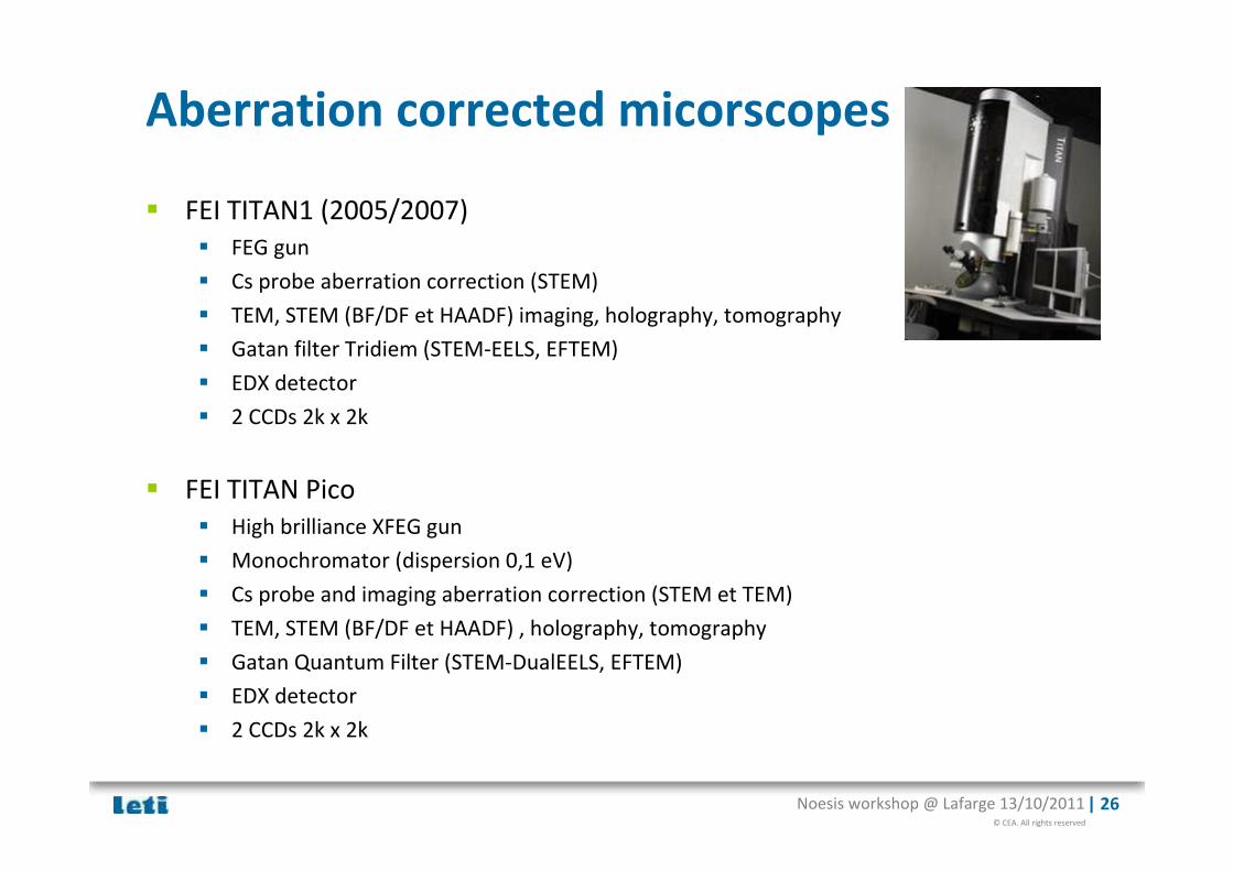
Aberration corrected micorscopes
� FEI TITAN1 (2005/2007)
� FEG gun
� Cs probe aberration correction (STEM)
� TEM, STEM (BF/DF et HAADF) imaging, holography, tomography
� Gatan filter Tridiem (STEM-EELS, EFTEM)
� EDX detector
� 2 CCDs 2k x 2k
� FEI TITAN Pico
� High brilliance XFEG gun
� Monochromator (dispersion 0,1 eV)
� Cs probe and imaging aberration correction (STEM et TEM)
� TEM, STEM (BF/DF et HAADF) , holography, tomography
� Gatan Quantum Filter (STEM-DualEELS, EFTEM)
� EDX detector
� 2 CCDs 2k x 2k

© CEA. All rights reserved
Noesis workshop @ Lafarge 13/10/2011 | 27
71 HAADF images (@ 300 kV with α = 15 mrad)acquired between -73 and +70°
Gate all around transistors
10nm TiN
3nm Hf02
15nm SiGe
SiN hard mask
SiGe wires

© CEA. All rights reserved
Noesis workshop @ Lafarge 13/10/2011 | 28
Destructive tomography
� Reasons for a sample to be precious � Only one sample exists (e.g. cultural heritage)
� Sequential analyses of the same sample by different probes
� X-rays and electrons radiation damage…
� Samples may often be destroyed� Microelectronics: billions of device per wafer
� Materials science: “random” ROI
� Alloys, polymers, cements
� Biology: selection of a few cells out of a large population of cells

© CEA. All rights reserved
Noesis workshop @ Lafarge 13/10/2011 | 29
From Uchic and HolzerMRS Bulletin 2007
« Slice and view » FIB nano-tomography

© CEA. All rights reserved
Noesis workshop @ Lafarge 13/10/2011 | 30
Zeta FIB column (Ga+)• Resolution 4 nm @ 30 kV / 0.1 pA• Accelerating voltage 1 kV to 30 kV• Current 0.1 pA to 45 nA @ 30 kV
Four channelGas Injection System• TEOS, C, Pt deposits• Liquid, solid state
and gas precursors
Gemini FEG SEM columnResolution 1.1 nm @ 20 kV and 2.5 nm @ 1 kV Accelerating voltage 100 V to 30 kVProbe current 4 pA to 20 nA
In-lens SE and EsBGood low-voltage performance
EDX (Brucker)
SE and SI
STEMBright field & dark field
Eucentric stageX 100 mm - Y 100 mm - Z 43 mmZ’ 10 mm - Tilt -10/+60°- R 360°6 motorized axisLoad lock 4”
QBSE
Detectors :
« Slice and view » FIB nano-tomography

© CEA. All rights reserved
Noesis workshop @ Lafarge 13/10/2011 | 31
« Slice and view » FIB nano-tomography
� Robust technique
� Works well both for large volumes @ nm resolution� No reconstruction, no local tomography
� Orientation & chemical contrast � SE & BSE images at low voltage
� Great potential� FIB-SEM � 3D morphology
� FIB-SEM-EDX � 3D chemical imaging
� FIB-SEM-EBSD � 3D grain & strain imaging

© CEA. All rights reserved
Noesis workshop @ Lafarge 13/10/2011 | 32
� Why sub-nanometer tomography in micro & nanoelectronics ?� 32 nm node (2010), 22nm (2011), 16nm (2013), 11nm (2015)
� Devices are now 3D !
� Multigate, tri gate, gate all around transistors
� Seeing, locating and identifying atoms in 3D becomes important
� Only 3D analytical technique available� Atom Probe Tomography (ancestor of Field Ion Microscopy)
Sub-nanometer tomography
DrainGate
Source

© CEA. All rights reserved
Noesis workshop @ Lafarge 13/10/2011 | 33
� Principle � Cryogenically-cooled needle shaped sample
� UHV + trace gas
� Progressive evaporation of surface atoms
� Pulsed voltage
� Recent evolutions� Position sensitive detector
� 2D depth resolved mapping
� Pulsed LASER
� Time of flight spectrometer
� Chemically sensitive
� 10 millions of atoms !
Atom Probe Tomography
Miller & Forbes, Mat. Charac. (2009)

© CEA. All rights reserved
Noesis workshop @ Lafarge 13/10/2011 | 34
Atom Probe Tomography
� Spatial resolutions� X,Y resolution ~ 0.1-0.3nm
� Z resolution ~0.3-0.5nm
� Detection efficiency ~60%
� Volume ~200,000nm3/hr
� FoV ~ 2000nm

© CEA. All rights reserved
Noesis workshop @ Lafarge 13/10/2011 | 35
Towards Nanometer3
Resolution
Probedvolume
100nm 1µµµµm
1000mm3
1000 µµµµ m3
1000nm3
Hard x-rayMicrotomography
Towards hard x-rayNanotomography
Electron & FIBNanotomography
Atom ProbeTomography
10nm1 A
5µm
Si
Cu Void
γγγγ-ray and neutronTomography
1mm
10nm

© CEA. All rights reserved
Noesis workshop @ Lafarge 13/10/2011 | 36
� Georg Haberfehlner (CEA-LETI)
� Matt Smith (MIT)
� Romain Quey (ex-CEA-LETI, now CNRS)
� Gérard Delette (CEA-LITEN)
� Jérôme Laurencin(CEA-LITEN)
� Pierre-Henri Jouneau(CEA-INAC)
� Adeline Grenier(CEA-LETI)
� Vincent Delaye
� Peter Cloetens (ESRF)
� Heikki Suhonen (ESRF)
� Jean-Louis Hodeau (CNRS)
� Frédéric Souchon (CEA-LETI)
� Patrick Leduc (CEA-LETI)
� Julien Bertheau (ST Microelectronics)
� Jean Charbonnier (CEA-LETI)
� And the Noesis & Lafarge organizers
Thanks to…