Embed Size (px)
Citation preview

1
Data sheet acquired from Harris SemiconductorSCHS135F
Features
• True and Complementary Outputs
• Buffered Inputs and Outputs
• Fanout (Over Temperature Range)- Standard Outputs . . . . . . . . . . . . . . . 10 LSTTL Loads- Bus Driver Outputs . . . . . . . . . . . . . 15 LSTTL Loads
• Wide Operating Temperature Range . . . -55oC to 125oC
• Balanced Propagation Delay and Transition Times
• Significant Power Reduction Compared to LSTTLLogic ICs
• HC Types- 2V to 6V Operation- High Noise Immunity: NIL = 30%, NIH = 30% of VCC
at VCC = 5V
• HCT Types- 4.5V to 5.5V Operation- Direct LSTTL Input Logic Compatibility,
VIL= 0.8V (Max), VIH = 2V (Min)- CMOS Input Compatibility, Il ≤ 1µA at VOL, VOH
Description
The ’HC75 and ’HCT75 are dual 2-bit bistable transparentlatches. Each one of the 2-bit latches is controlled byseparate Enable inputs (1E and 2E) which are active LOW.When the Enable input is HIGH data enters the latch andappears at the Q output. When the Enable input (1E and 2E)is LOW the output is not affected.
PinoutCD54HC75, CD54HCT75 (CERDIP)
CD74HC75 (PDIP, SOIC, SOP, TSSOP)CD74HCT75 (PDIP, SOIC, TSSOP)
TOP VIEW
Ordering Information
PART NUMBERTEMP. RANGE
(oC) PACKAGE
CD54HC75F3A -55 to 125 16 Ld CERDIP
CD54HCT75F3A -55 to 125 16 Ld CERDIP
CD74HC75E -55 to 125 16 Ld PDIP
CD74HC75M -55 to 125 16 Ld SOIC
CD74HC75MT -55 to 125 16 Ld SOIC
CD74HC75M96 -55 to 125 16 Ld SOIC
CD74HC75NSR -55 to 125 16 Ld SOP
CD74HC75PW -55 to 125 16 Ld TSSOP
CD74HC75PWR -55 to 125 16 Ld TSSOP
CD74HCT75E -55 to 125 16 Ld PDIP
CD74HCT75M -55 to 125 16 Ld SOIC
CD74HCT75PWT -55 to 125 16 Ld TSSOP
NOTE: When ordering, use the entire part number. The suffixes 96and R denote tape and reel. The suffix T denotes a small-quantityreel of 250.
14
15
16
9
13
12
11
10
1
2
3
4
5
7
6
8
1Q0
1D0
1D1
2E
VCC
2D0
2Q1
2D1
1Q0
1Q1
1E
GND
2Q0
2Q0
2Q1
1Q1
March 1998 - Revised October 2003
CAUTION: These devices are sensitive to electrostatic discharge. Users should follow proper IC Handling Procedures.
Copyright © 2003, Texas Instruments Incorporated
CD54HC75, CD74HC75,CD54HCT75, CD74HCT75
Dual 2-Bit BistableTransparent Latch
[ /Title(CD74HC75,CD74HCT75)/Sub-ject(Dual2-BitBistable

2
Functional Diagram
Logic Diagram
TRUTH TABLE
INPUTS OUTPUTS
D E Q Q
L H L H
H H H L
X L Q0 Q0
H= High LevelL= Low LevelX= Don’t CareQ0 = The level of Q before the transition of E.
D02 (6)
3 (7)
16 (10)
Q1
Q0
D1
13 (4)E
1 (11)
14 (8)
15 (9)
Q0
Q1
1 OF 2LATCHES
FIGURE 1. LOGIC DIAGRAM FIGURE 2. LATCH DETAIL
D0
3 (7)
2 (6)LATCH 0
QD
LE LE
16 (10)
1 (11)
Q0
Q0
E
13 (4)
LATCH 1
QD
LE LE
D1
14 (8)
Q1
15 (9)Q1
5
12GND
VCC
P
N
LE
LE Q
P
N
LE
LE
Q
CD54HC75, CD74HC75, CD54HCT75, CD74HCT75

3
Absolute Maximum Ratings Thermal InformationDC Supply Voltage, VCC . . . . . . . . . . . . . . . . . . . . . . . . -0.5V to 7VDC Input Diode Current, IIK
For VI < -0.5V or VI > VCC + 0.5V . . . . . . . . . . . . . . . . . . . . . .±20mADC Drain Current, per Output, IO
For -0.5V < VO < VCC + 0.5V . . . . . . . . . . . . . . . . . . . . . . . . . .±25mADC Output Diode Current, IOK
For VO < -0.5V or VO > VCC + 0.5V . . . . . . . . . . . . . . . . . . . .±20mADC Output Source or Sink Current per Output Pin, IO
For VO > -0.5V or VO < VCC + 0.5V . . . . . . . . . . . . . . . . . . . .±25mADC VCC or Ground Current, ICC . . . . . . . . . . . . . . . . . . . . . . . . .±50mA
Operating ConditionsTemperature Range, TA . . . . . . . . . . . . . . . . . . . . . . -55oC to 125oCSupply Voltage Range, VCC
HC Types . . . . . . . . . . . . . . . . . . . . . . . . . . . . . . . . . . . . .2V to 6VHCT Types . . . . . . . . . . . . . . . . . . . . . . . . . . . . . . . . .4.5V to 5.5V
DC Input or Output Voltage, VI, VO . . . . . . . . . . . . . . . . . 0V to VCCInput Rise and Fall Time
2V . . . . . . . . . . . . . . . . . . . . . . . . . . . . . . . . . . . . . . 1000ns (Max)4.5V. . . . . . . . . . . . . . . . . . . . . . . . . . . . . . . . . . . . . . 500ns (Max)6V . . . . . . . . . . . . . . . . . . . . . . . . . . . . . . . . . . . . . . . 400ns (Max)
Package Thermal Impedance, θJA (see Note 1)
E (PDIP) package . . . . . . . . . . . . . . . . . . . . . . . . . . . . . .67oC/WM (SOIC) package . . . . . . . . . . . . . . . . . . . . . . . . . . . . . .73oC/WNS (SOP) package . . . . . . . . . . . . . . . . . . . . . . . . . . . . .64oC/WPW (TSSOP) package. . . . . . . . . . . . . . . . . . . . . . . . . .108oC/W
Maximum Junction Temperature (Hermetic Package or Die) . . . 175oCMaximum Junction Temperature (Plastic Package) . . . . . . . . 150oCMaximum Storage Temperature Range . . . . . . . . . .-65oC to 150oCMaximum Lead Temperature (Soldering 10s) . . . . . . . . . . . . . 300oC
(SOIC - Lead Tips Only)
CAUTION: Stresses above those listed in “Absolute Maximum Ratings” may cause permanent damage to the device. This is a stress only rating and operationof the device at these or any other conditions above those indicated in the operational sections of this specification is not implied.
NOTE:
1. The package thermal impedance is calculated in accordance with JESD 51-7.
DC Electrical Specifications
PARAMETER SYMBOL
TESTCONDITIONS
VCC (V)
25oC -40oC TO 85oC -55oC TO 125oC
UNITSVI (V) IO (mA) MIN TYP MAX MIN MAX MIN MAX
HC TYPES
High Level InputVoltage
VIH - - 2 1.5 - - 1.5 - 1.5 - V
4.5 3.15 - - 3.15 - 3.15 - V
6 4.2 - - 4.2 - 4.2 - V
Low Level InputVoltage
VIL - - 2 - - 0.5 - 0.5 - 0.5 V
4.5 - - 1.35 - 1.35 - 1.35 V
6 - - 1.8 - 1.8 - 1.8 V
High Level OutputVoltageCMOS Loads
VOH VIH orVIL
-0.02 2 1.9 - - 1.9 - 1.9 - V
4.5 4.4 - - 4.4 - 4.4 - V
6 5.9 - - 5.9 - 5.9 - V
High Level OutputVoltageTTL Loads
- - - - - - - - - V
-4 4.5 3.98 - - 3.84 - 3.7 - V
-5.2 6 5.48 - - 5.34 - 5.2 - V
Low Level OutputVoltageCMOS Loads
VOL VIH orVIL
0.02 2 - - 0.1 - 0.1 - 0.1 V
4.5 - - 0.1 - 0.1 - 0.1 V
6 - - 0.1 - 0.1 - 0.1 V
Low Level OutputVoltageTTL Loads
- - - - - - - - - V
4 4.5 - - 0.26 - 0.33 - 0.4 V
5.2 6 - - 0.26 - 0.33 - 0.4 V
Input LeakageCurrent
II VCC orGND
- 6 - - ±0.1 - ±1 - ±1 µA
CD54HC75, CD74HC75, CD54HCT75, CD74HCT75

4
Quiescent DeviceCurrent
ICC VCC orGND
0 6 - - 4 - 40 - 80 µA
HCT TYPES
High Level InputVoltage
VIH - - 4.5 to5.5
2 - - 2 - 2 - V
Low Level InputVoltage
VIL - - 4.5 to5.5
- - 0.8 - 0.8 - 0.8 V
High Level OutputVoltageCMOS Loads
VOH VIH orVIL
- 0.02 4.5 4.4 - - 4.4 - 4.4 - V
High Level OutputVoltageTTL Loads
-4 4.5 3.98 - - 3.84 - 3.7 - V
Low Level OutputVoltage CMOS Loads
VOL VIH orVIL
0.02 4.5 - - 0.1 - 0.1 - 0.1 V
Low Level OutputVoltageTTL Loads
4 4.5 - - 0.26 - 0.33 - 0.4 V
Input LeakageCurrent
II VCCandGND
- 5.5 - ±0.1 - ±1 - ±1 µA
Quiescent DeviceCurrent
ICC VCC orGND
0 5.5 - - 4 - 40 - 80 µA
Additional QuiescentDevice Current PerInput Pin: 1 Unit Load
∆ICC(Note 2)
VCC- 2.1
- 4.5 to5.5
- 100 360 - 450 - 490 µA
NOTE:
2. For dual-supply systems theoretical worst case (VI = 2.4V, VCC = 5.5V) specification is 1.8mA.
DC Electrical Specifications (Continued)
PARAMETER SYMBOL
TESTCONDITIONS
VCC (V)
25oC -40oC TO 85oC -55oC TO 125oC
UNITSVI (V) IO (mA) MIN TYP MAX MIN MAX MIN MAX
HCT Input Loading Table
INPUT UNIT LOADS
D0, D1 0.8
1E, 2E 1.2
NOTE: Unit Load is ∆ICC limit specified in DC Electrical Specifica-tions table, e.g., 360µA max at 25oC.
Prerequisite For Switching Specifications
PARAMETER SYMBOLTEST
CONDITIONSVCC(V)
25oC -40oC TO 85oC -55oC TO 125oC
UNITSMIN TYP MAX MIN MAX MIN MAX
HC TYPES
Pulse Width Enable Input tW - 2 80 - - 100 - 120 - ns
4.5 16 - - 20 - 24 - ns
6 14 - - 17 - 20 - ns
Setup Time D to Enable tSU - 2 60 - - 75 - 90 - ns
4.5 12 - - 15 - 18 - ns
6 10 - - 13 - 15 - ns
CD54HC75, CD74HC75, CD54HCT75, CD74HCT75

5
Hold Time Enable to D tH - 2 3 - - 3 - 3 - ns
4.5 3 - - 3 - 3 - ns
6 3 - - 3 - 3 - ns
HCT TYPES
Pulse Width Enable Input tW - 4.5 16 - - 20 - 24 - ns
Setup Time D to Enable tSU - 4.5 12 - - 15 - 18 - ns
Hold Time Enable to D tH - 4.5 3 - - 3 - 3 - ns
Switching Specifications Input tr, tf = 6ns
PARAMETER SYMBOLTEST
CONDITIONSVCC(V)
25oC -40oC TO 85oC -55oC TO 125oC
UNITSMIN TYP MAX MIN MAX MIN MAX
HC TYPES
Propagation Delay,Data to Q
tPLH, tPHL CL = 50pF 2 - - 110 - 140 - 165 ns
CL = 50pF 4.5 - - 22 - 28 - 33 ns
CL = 15pF 5 - 9 - - - - - ns
CL = 50pF 6 - - 19 - 24 - 28 ns
Propagation Delay,Data to Q
tPLH, tPHL CL = 50pF 2 - - 130 - 165 - 195 ns
CL = 50pF 4.5 - - 26 - 33 - 39 ns
CL = 15pF 5 - 10 - - - - - ns
CL = 50pF 6 - - 22 - 28 - 33 ns
Propagation Delay,Enable to Q
tPLH, tPHL CL = 50pF 2 - - 130 - 165 - 195 ns
CL = 50pF 4.5 - - 26 - 33 - 39 ns
CL = 15pF 5 - 10 - - - - - ns
CL = 50pF 6 - - 22 - 28 - 33 ns
Propagation Delay,Enable to Q
tPLH, tPHL CL = 50pF 2 - - 130 - 165 - 195 ns
CL = 50pF 4.5 - - 26 - 33 - 39 ns
CL = 15pF 5 - 11 - - - - - ns
CL = 50pF 6 - - 22 - 28 - 33 ns
Output Transition Time tTLH, tTHL CL = 50pF 2 - - 75 - 95 - 110 ns
CL = 50pF 4.5 - - 15 - 19 - 22 ns
CL = 50pF 6 - - 13 - 16 - 19 ns
Input Capacitance CI - - - - 10 - 10 - 10 pF
Power Dissipation Capacitance(Notes 3, 4)
CPD - 5 - 46 - - - - - pF
HCT TYPES
Propagation Delay,Data to Q
tPLH, tPHL CL = 50pF 4.5 - - 28 - 35 - 42 ns
CL = 15pF 5 - 11 - - - - - ns
Propagation Delay,Data to Q
tPLH, tPHL CL = 50pF 4.5 - - 28 - 35 - 42 ns
CL = 15pF 5 - 11 - - - - - ns
Propagation Delay,Enable to Q
tPLH, tPHL CL = 50pF 4.5 - - 28 - 35 - 42 ns
CL = 15pF 5 11 - - - - - ns
Prerequisite For Switching Specifications (Continued)
PARAMETER SYMBOLTEST
CONDITIONSVCC(V)
25oC -40oC TO 85oC -55oC TO 125oC
UNITSMIN TYP MAX MIN MAX MIN MAX
CD54HC75, CD74HC75, CD54HCT75, CD74HCT75

6
Propagation Delay,Enable to Q
tPLH, tPHL CL = 50pF 4.5 - - 30 - 38 - 45 ns
CL = 15pF 5 - 12 - - - - - ns
Output Transition Time tTLH, tTHL CL = 50pF 4.5 - - 15 - 19 - 22 ns
Input Capacitance CI - - - - 10 - 10 - 10 pF
Power Dissipation Capacitance(Notes 3, 4)
CPD - 5 - 46 - - - - - pF
NOTES:
3. CPD is used to determine the dynamic power consumption, per latch.
4. PD = VCC2 fi (CPD + CL) where fi = input frequency, CL = output load capacitance, VCC = supply voltage.
Switching Specifications Input tr, tf = 6ns (Continued)
PARAMETER SYMBOLTEST
CONDITIONSVCC(V)
25oC -40oC TO 85oC -55oC TO 125oC
UNITSMIN TYP MAX MIN MAX MIN MAX
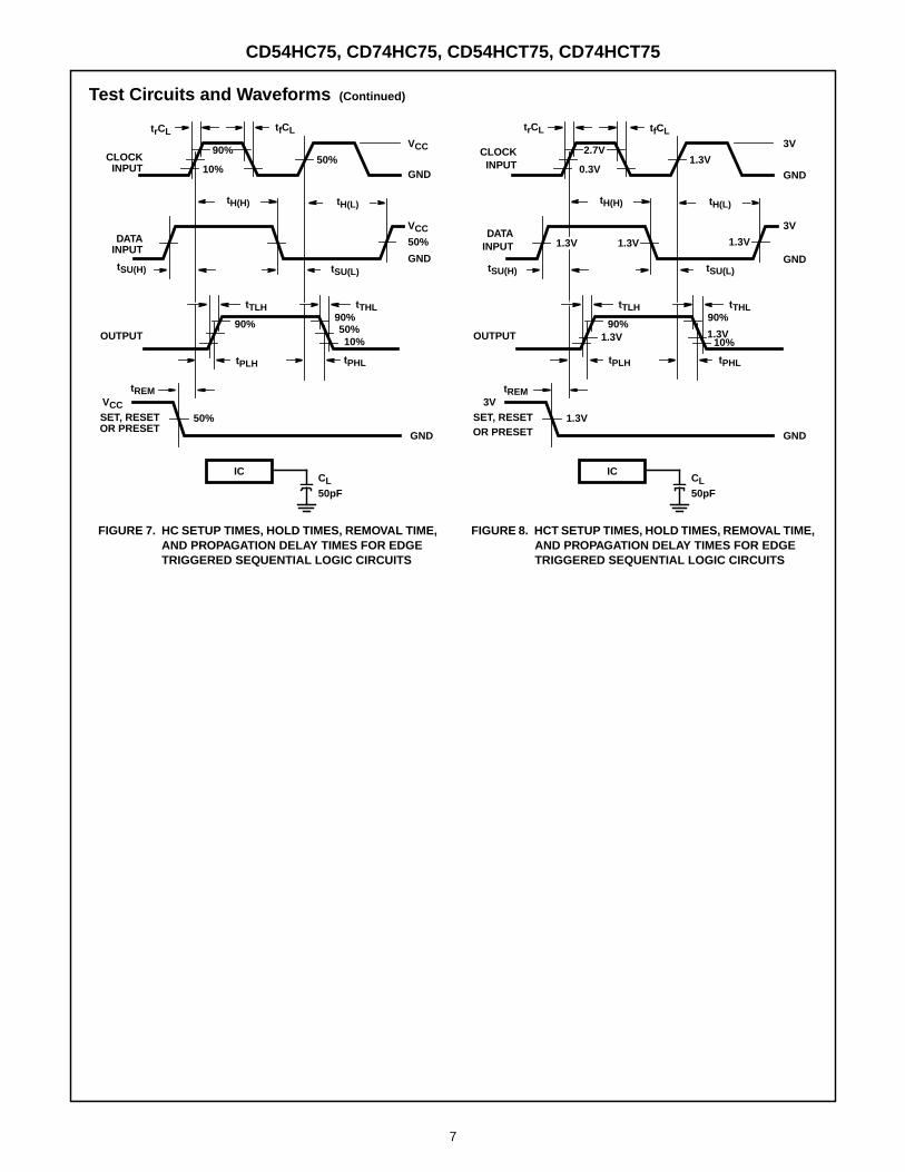
Test Circuits and Waveforms
NOTE: Outputs should be switching from 10% VCC to 90% VCC inaccordance with device truth table. For fMAX, input duty cycle = 50%.
FIGURE 3. HC CLOCK PULSE RISE AND FALL TIMES ANDPULSE WIDTH
NOTE: Outputs should be switching from 10% VCC to 90% VCC inaccordance with device truth table. For fMAX, input duty cycle = 50%.
FIGURE 4. HCT CLOCK PULSE RISE AND FALL TIMES ANDPULSE WIDTH
FIGURE 5. HC AND HCU TRANSITION TIMES AND PROPAGA-TION DELAY TIMES, COMBINATION LOGIC
FIGURE 6. HCT TRANSITION TIMES AND PROPAGATIONDELAY TIMES, COMBINATION LOGIC
CLOCK 90%50%
10% GND
VCC
trCL tfCL
50% 50%
tWL tWH
10%
tWL + tWH =fCL
I
CLOCK 2.7V1.3V
0.3V GND
3V
trCL = 6nstfCL = 6ns
1.3V 1.3V
tWL tWH
0.3V
tWL + tWH =fCL
I
tPHL tPLH
tTHL tTLH
90%50%10%
50%10%INVERTING
OUTPUT
INPUT
GND
VCC
tr = 6ns tf = 6ns
90%
tPHL tPLH
tTHL tTLH
2.7V1.3V0.3V
1.3V10%INVERTING
OUTPUT
INPUT
GND
3V
tr = 6ns tf = 6ns
90%
CD54HC75, CD74HC75, CD54HCT75, CD74HCT75
7
FIGURE 7. HC SETUP TIMES, HOLD TIMES, REMOVAL TIME,AND PROPAGATION DELAY TIMES FOR EDGETRIGGERED SEQUENTIAL LOGIC CIRCUITS
FIGURE 8. HCT SETUP TIMES, HOLD TIMES, REMOVAL TIME,AND PROPAGATION DELAY TIMES FOR EDGETRIGGERED SEQUENTIAL LOGIC CIRCUITS
Test Circuits and Waveforms (Continued)
trCL tfCL
GND
VCC
GND
VCC50%
90%
10%
GND
CLOCKINPUT
DATAINPUT
OUTPUT
SET, RESETOR PRESET
VCC50%
50%
90%
10%50%
90%
tREM
tPLH
tSU(H)
tTLH tTHL
tH(L)
tPHL
ICCL50pF
tSU(L)
tH(H)
trCL tfCL
GND
3V
GND
3V
1.3V2.7V
0.3V
GND
CLOCKINPUT
DATAINPUT
OUTPUT
SET, RESETOR PRESET
3V
1.3V
1.3V1.3V
90%
10%1.3V
90%
tREM
tPLH
tSU(H)
tTLH tTHL
tH(L)
tPHL
ICCL50pF
tSU(L)
1.3V
tH(H)
1.3V
CD54HC75, CD74HC75, CD54HCT75, CD74HCT75

PACKAGING INFORMATION
Orderable Device Status (1) PackageType
PackageDrawing
Pins PackageQty
Eco Plan (2) Lead/Ball Finish MSL Peak Temp (3)
5962-9075801MEA ACTIVE CDIP J 16 1 TBD A42 N / A for Pkg Type
8407001EA ACTIVE CDIP J 16 1 TBD A42 N / A for Pkg Type
CD54HC75F3A ACTIVE CDIP J 16 1 TBD A42 N / A for Pkg Type
CD54HCT75F3A ACTIVE CDIP J 16 1 TBD A42 N / A for Pkg Type
CD74HC75E ACTIVE PDIP N 16 25 Pb-Free(RoHS)
CU NIPDAU N / A for Pkg Type
CD74HC75EE4 ACTIVE PDIP N 16 25 Pb-Free(RoHS)
CU NIPDAU N / A for Pkg Type
CD74HC75M ACTIVE SOIC D 16 40 Green (RoHS &no Sb/Br)
CU NIPDAU Level-1-260C-UNLIM
CD74HC75M96 ACTIVE SOIC D 16 2500 Green (RoHS &no Sb/Br)
CU NIPDAU Level-1-260C-UNLIM
CD74HC75M96E4 ACTIVE SOIC D 16 2500 Green (RoHS &no Sb/Br)
CU NIPDAU Level-1-260C-UNLIM
CD74HC75M96G4 ACTIVE SOIC D 16 2500 Green (RoHS &no Sb/Br)
CU NIPDAU Level-1-260C-UNLIM
CD74HC75ME4 ACTIVE SOIC D 16 40 Green (RoHS &no Sb/Br)
CU NIPDAU Level-1-260C-UNLIM
CD74HC75MG4 ACTIVE SOIC D 16 40 Green (RoHS &no Sb/Br)
CU NIPDAU Level-1-260C-UNLIM
CD74HC75MT ACTIVE SOIC D 16 250 Green (RoHS &no Sb/Br)
CU NIPDAU Level-1-260C-UNLIM
CD74HC75MTE4 ACTIVE SOIC D 16 250 Green (RoHS &no Sb/Br)
CU NIPDAU Level-1-260C-UNLIM
CD74HC75MTG4 ACTIVE SOIC D 16 250 Green (RoHS &no Sb/Br)
CU NIPDAU Level-1-260C-UNLIM
CD74HC75NSR ACTIVE SO NS 16 2000 Green (RoHS &no Sb/Br)
CU NIPDAU Level-1-260C-UNLIM
CD74HC75NSRE4 ACTIVE SO NS 16 2000 Green (RoHS &no Sb/Br)
CU NIPDAU Level-1-260C-UNLIM
CD74HC75NSRG4 ACTIVE SO NS 16 2000 Green (RoHS &no Sb/Br)
CU NIPDAU Level-1-260C-UNLIM
CD74HC75PW ACTIVE TSSOP PW 16 90 Green (RoHS &no Sb/Br)
CU NIPDAU Level-1-260C-UNLIM
CD74HC75PWE4 ACTIVE TSSOP PW 16 90 Green (RoHS &no Sb/Br)
CU NIPDAU Level-1-260C-UNLIM
CD74HC75PWG4 ACTIVE TSSOP PW 16 90 Green (RoHS &no Sb/Br)
CU NIPDAU Level-1-260C-UNLIM
CD74HC75PWR ACTIVE TSSOP PW 16 2000 Green (RoHS &no Sb/Br)
CU NIPDAU Level-1-260C-UNLIM
CD74HC75PWRE4 ACTIVE TSSOP PW 16 2000 Green (RoHS &no Sb/Br)
CU NIPDAU Level-1-260C-UNLIM
CD74HC75PWRG4 ACTIVE TSSOP PW 16 2000 Green (RoHS &no Sb/Br)
CU NIPDAU Level-1-260C-UNLIM
CD74HC75PWT ACTIVE TSSOP PW 16 250 Green (RoHS &no Sb/Br)
CU NIPDAU Level-1-260C-UNLIM
CD74HC75PWTE4 ACTIVE TSSOP PW 16 250 Green (RoHS &no Sb/Br)
CU NIPDAU Level-1-260C-UNLIM
CD74HC75PWTG4 ACTIVE TSSOP PW 16 250 Green (RoHS & CU NIPDAU Level-1-260C-UNLIM
PACKAGE OPTION ADDENDUM
www.ti.com 15-Oct-2009
Addendum-Page 1

Orderable Device Status (1) PackageType
PackageDrawing
Pins PackageQty
Eco Plan (2) Lead/Ball Finish MSL Peak Temp (3)
no Sb/Br)
CD74HCT75E ACTIVE PDIP N 16 25 Pb-Free(RoHS)
CU NIPDAU N / A for Pkg Type
CD74HCT75EE4 ACTIVE PDIP N 16 25 Pb-Free(RoHS)
CU NIPDAU N / A for Pkg Type
CD74HCT75M ACTIVE SOIC D 16 40 Green (RoHS &no Sb/Br)
CU NIPDAU Level-1-260C-UNLIM
CD74HCT75ME4 ACTIVE SOIC D 16 40 Green (RoHS &no Sb/Br)
CU NIPDAU Level-1-260C-UNLIM
CD74HCT75MG4 ACTIVE SOIC D 16 40 Green (RoHS &no Sb/Br)
CU NIPDAU Level-1-260C-UNLIM
(1) The marketing status values are defined as follows:ACTIVE: Product device recommended for new designs.LIFEBUY: TI has announced that the device will be discontinued, and a lifetime-buy period is in effect.NRND: Not recommended for new designs. Device is in production to support existing customers, but TI does not recommend using this part ina new design.PREVIEW: Device has been announced but is not in production. Samples may or may not be available.OBSOLETE: TI has discontinued the production of the device.
(2) Eco Plan - The planned eco-friendly classification: Pb-Free (RoHS), Pb-Free (RoHS Exempt), or Green (RoHS & no Sb/Br) - please checkhttp://www.ti.com/productcontent for the latest availability information and additional product content details.TBD: The Pb-Free/Green conversion plan has not been defined.Pb-Free (RoHS): TI's terms "Lead-Free" or "Pb-Free" mean semiconductor products that are compatible with the current RoHS requirementsfor all 6 substances, including the requirement that lead not exceed 0.1% by weight in homogeneous materials. Where designed to be solderedat high temperatures, TI Pb-Free products are suitable for use in specified lead-free processes.Pb-Free (RoHS Exempt): This component has a RoHS exemption for either 1) lead-based flip-chip solder bumps used between the die andpackage, or 2) lead-based die adhesive used between the die and leadframe. The component is otherwise considered Pb-Free (RoHScompatible) as defined above.Green (RoHS & no Sb/Br): TI defines "Green" to mean Pb-Free (RoHS compatible), and free of Bromine (Br) and Antimony (Sb) based flameretardants (Br or Sb do not exceed 0.1% by weight in homogeneous material)
(3) MSL, Peak Temp. -- The Moisture Sensitivity Level rating according to the JEDEC industry standard classifications, and peak soldertemperature.
Important Information and Disclaimer:The information provided on this page represents TI's knowledge and belief as of the date that it isprovided. TI bases its knowledge and belief on information provided by third parties, and makes no representation or warranty as to theaccuracy of such information. Efforts are underway to better integrate information from third parties. TI has taken and continues to takereasonable steps to provide representative and accurate information but may not have conducted destructive testing or chemical analysis onincoming materials and chemicals. TI and TI suppliers consider certain information to be proprietary, and thus CAS numbers and other limitedinformation may not be available for release.
In no event shall TI's liability arising out of such information exceed the total purchase price of the TI part(s) at issue in this document sold by TIto Customer on an annual basis.
PACKAGE OPTION ADDENDUM
www.ti.com 15-Oct-2009
Addendum-Page 2

TAPE AND REEL INFORMATION
*All dimensions are nominal
Device PackageType
PackageDrawing
Pins SPQ ReelDiameter
(mm)
ReelWidth
W1 (mm)
A0 (mm) B0 (mm) K0 (mm) P1(mm)
W(mm)
Pin1Quadrant
CD74HC75M96 SOIC D 16 2500 330.0 16.4 6.5 10.3 2.1 8.0 16.0 Q1
CD74HC75NSR SO NS 16 2000 330.0 16.4 8.2 10.5 2.5 12.0 16.0 Q1
CD74HC75PWR TSSOP PW 16 2000 330.0 12.4 7.0 5.6 1.6 8.0 12.0 Q1
PACKAGE MATERIALS INFORMATION
www.ti.com 19-Mar-2008
Pack Materials-Page 1

*All dimensions are nominal
Device Package Type Package Drawing Pins SPQ Length (mm) Width (mm) Height (mm)
CD74HC75M96 SOIC D 16 2500 333.2 345.9 28.6
CD74HC75NSR SO NS 16 2000 346.0 346.0 33.0
CD74HC75PWR TSSOP PW 16 2000 346.0 346.0 29.0
PACKAGE MATERIALS INFORMATION
www.ti.com 19-Mar-2008
Pack Materials-Page 2

MECHANICAL DATA
MTSS001C – JANUARY 1995 – REVISED FEBRUARY 1999
POST OFFICE BOX 655303 • DALLAS, TEXAS 75265
PW (R-PDSO-G**) PLASTIC SMALL-OUTLINE PACKAGE14 PINS SHOWN
0,65 M0,10
0,10
0,25
0,500,75
0,15 NOM
Gage Plane
28
9,80
9,60
24
7,90
7,70
2016
6,60
6,40
4040064/F 01/97
0,30
6,606,20
8
0,19
4,304,50
7
0,15
14
A
1
1,20 MAX
14
5,10
4,90
8
3,10
2,90
A MAX
A MIN
DIMPINS **
0,05
4,90
5,10
Seating Plane
0°–8°
NOTES: A. All linear dimensions are in millimeters.B. This drawing is subject to change without notice.C. Body dimensions do not include mold flash or protrusion not to exceed 0,15.D. Falls within JEDEC MO-153


IMPORTANT NOTICETexas Instruments Incorporated and its subsidiaries (TI) reserve the right to make corrections, modifications, enhancements, improvements,and other changes to its products and services at any time and to discontinue any product or service without notice. Customers shouldobtain the latest relevant information before placing orders and should verify that such information is current and complete. All products aresold subject to TI’s terms and conditions of sale supplied at the time of order acknowledgment.TI warrants performance of its hardware products to the specifications applicable at the time of sale in accordance with TI’s standardwarranty. Testing and other quality control techniques are used to the extent TI deems necessary to support this warranty. Except wheremandated by government requirements, testing of all parameters of each product is not necessarily performed.TI assumes no liability for applications assistance or customer product design. Customers are responsible for their products andapplications using TI components. To minimize the risks associated with customer products and applications, customers should provideadequate design and operating safeguards.TI does not warrant or represent that any license, either express or implied, is granted under any TI patent right, copyright, mask work right,or other TI intellectual property right relating to any combination, machine, or process in which TI products or services are used. Informationpublished by TI regarding third-party products or services does not constitute a license from TI to use such products or services or awarranty or endorsement thereof. Use of such information may require a license from a third party under the patents or other intellectualproperty of the third party, or a license from TI under the patents or other intellectual property of TI.Reproduction of TI information in TI data books or data sheets is permissible only if reproduction is without alteration and is accompaniedby all associated warranties, conditions, limitations, and notices. Reproduction of this information with alteration is an unfair and deceptivebusiness practice. TI is not responsible or liable for such altered documentation. Information of third parties may be subject to additionalrestrictions.Resale of TI products or services with statements different from or beyond the parameters stated by TI for that product or service voids allexpress and any implied warranties for the associated TI product or service and is an unfair and deceptive business practice. TI is notresponsible or liable for any such statements.TI products are not authorized for use in safety-critical applications (such as life support) where a failure of the TI product would reasonablybe expected to cause severe personal injury or death, unless officers of the parties have executed an agreement specifically governingsuch use. Buyers represent that they have all necessary expertise in the safety and regulatory ramifications of their applications, andacknowledge and agree that they are solely responsible for all legal, regulatory and safety-related requirements concerning their productsand any use of TI products in such safety-critical applications, notwithstanding any applications-related information or support that may beprovided by TI. Further, Buyers must fully indemnify TI and its representatives against any damages arising out of the use of TI products insuch safety-critical applications.TI products are neither designed nor intended for use in military/aerospace applications or environments unless the TI products arespecifically designated by TI as military-grade or "enhanced plastic." Only products designated by TI as military-grade meet militaryspecifications. Buyers acknowledge and agree that any such use of TI products which TI has not designated as military-grade is solely atthe Buyer's risk, and that they are solely responsible for compliance with all legal and regulatory requirements in connection with such use.TI products are neither designed nor intended for use in automotive applications or environments unless the specific TI products aredesignated by TI as compliant with ISO/TS 16949 requirements. Buyers acknowledge and agree that, if they use any non-designatedproducts in automotive applications, TI will not be responsible for any failure to meet such requirements.Following are URLs where you can obtain information on other Texas Instruments products and application solutions:Products ApplicationsAmplifiers amplifier.ti.com Audio www.ti.com/audioData Converters dataconverter.ti.com Automotive www.ti.com/automotiveDLP® Products www.dlp.com Broadband www.ti.com/broadbandDSP dsp.ti.com Digital Control www.ti.com/digitalcontrolClocks and Timers www.ti.com/clocks Medical www.ti.com/medicalInterface interface.ti.com Military www.ti.com/militaryLogic logic.ti.com Optical Networking www.ti.com/opticalnetworkPower Mgmt power.ti.com Security www.ti.com/securityMicrocontrollers microcontroller.ti.com Telephony www.ti.com/telephonyRFID www.ti-rfid.com Video & Imaging www.ti.com/videoRF/IF and ZigBee® Solutions www.ti.com/lprf Wireless www.ti.com/wireless
Mailing Address: Texas Instruments, Post Office Box 655303, Dallas, Texas 75265Copyright © 2009, Texas Instruments Incorporated