Embed Size (px)
Citation preview

i
Design of RISC Processor (64-bit) IP Core
Project Report Submitted in Partial Fulfillment of the Requirements for the
Degree of
BACHELOR OF TECHNOLOGY
IN
ELECTRONICS AND COMMUNICATION ENGINEERING
BY
ANUSHAVARSALA (09241A0463)
HEMA HARISHA PONNAM (09241A0474)
RADHIKA REDDY PEDDAMALLU (09241A0490)
YAMINI SINDHU BOTCHA (09241AO4C0)
Under the Esteemed Guidance of
Mr. Mannem kiran
Associate Professor
DEPARTMENT OF ELECTRONICS AND COMMUNICATION
ENGINEERING
GOKARAJU RANGARAJU INSTITUTE OF
ENGINEERING AN D TECHNOLOGY
(Affiliated to Jawaharlal Nehru Technological University)
HYDERABAD 500 090
2013

ii
Department of Electronics and Communication Engineering
Gokaraju Rangaraju Institute of Engineering and Technology
(Affiliated to Jawaharlal Nehru Technological University)
Hyderabad 500 090
2013
Certificate
This is to certify that this project report entitled Design of RISC
Processor (64bit) IP Core by Anusha (09241A0463), Harisha (09241A0474),Radhika
Reddy(09241A0490) Yamini Sindhu Botcha (Roll no 09241A04C0) submitted in
partial fulfillment of the requirements for the degree of Bachelor of Technology in
Electronics and Communication Engineering of the Jawaharlal Nehru Technological
University. Hyderabad, during academic year 2009-2013, is a bonafide record of work
carried out under our guidance and supervision.
M.Kiran Dr.Ravi Billa
Associate Professor (Head of Department)
(Internal Guide) (External Examiner)

iii
Acknowledgement
It is my pleasure to express thanks to Mr.M.Kiran for the encouragement
and guidance throughout the course of this project.
I thank Mr. Manchalla Omkara Venkata Pavan Kumar, Associate
professor helping us for the successful completion of the project.
I thank Mr. Ravi Billa, HOD ECE department for helping us for the
completion of project.
V. Anusha __________________
P. Hema Harisha __________________
P. Radhika __________________
B. Yamini Sindhu __________________

iv
Abstract
The RISC (Reduced Instruction Set Computer) is a CPU design strategy using small
instruction set compared to CISC (Complex Instruction Set Computer) processor. It is
designed to achieve faster execution of instructions, within one clock cycle. The RISC'
processor is designed to incorporate basic instructions involving Arithmetic, Logical, Data
Transfer and Control Instructions. All instruction will have simple register addressing. An
important aspect instruction set is that it is easy to decode (Fixed length instruction
format).Thus the OpCode and Instruction Register fields can be accessed simultaneously. To
implement these instructions the design incorporates various design blocks like Control Unit
(CU), Arithmetic Logic Unit (ALU), and Accumulator (ACC). Program Counter (PC).
Instruction Register (IR), Memory, Clock generator, Register and additional glue logic. The
Instruction format contains first four MSB bits as OPCOPDE and remaining 28bits as
Address bus. It can address 256Gbytes of memory location and 64-bit Bi-directional Data
Bus.
Implementation details
HDL : Verilog
Design : 64-bit (IP core)
Simulator : Cadence Tools

v
Contents
List of figures vii Abbreviations viii
Chapter1: INTRODUCTION 1 1.1 IP core 1 1.2 Aim of the Project 1
1.3 Methodology 2
Chapter 2: LITERATURE REVIEW 3
2.1 Introduction 4
2.2 Importance 9
2.3 Organization of the report 9
2.4 Application areas 10
2.5 Typical Design Flow 10
Chapter 3: IMPLEMENTATION 11
3.1 Description 11
3.2 Code 13
3.3 ALU (Arithmetic and Logic Unit) 13
3.3.1 Algorithm 14
3.3.2 Code 14
3.3.3 Code Explanation 14
3.3.4 Waveforms 16
3.3.5 Waveform Explanation 16
3.4 Memory 16
3.4.1 Algorithm 16
3.4.2 Code 16
3.4.3 Code Explanation 16
3.4.4 Waveforms 16
3.4.5 Waveform Explanation 17
3.5 Control and Decoder 17
3.5.1 Algorithm 17
3.5.2 Code 18
3.5.3 Code Explanation 21
3.5.4 Waveforms 21
3.5.5 Waveform Explanation 21
3.6 Program Counter 21
3.6.1 Algorithm 21
3.6.2 Code 22
3.6.3 Code Explanation 22
3.6.4 Waveforms 22
3.6.5 Waveform Explanation 22
3.7 Instruction Register 23
3.7.1 Algorithm 23
3.7.2 Code 23
3.7.3 Code Explanation 23
3.7.4 Waveforms 24
3.7.5 Waveform Explanation 24
3.8 Internal Register 25
3.8.1 Algorithm 25

vi
3.8.2 Code 25
3.8.3 Code Explanation 27
3.8.4 Waveforms: 27
3.8.5 Waveform Explanation 27
3.9 Tristate Buffer 27
3.9.1 Algorithm 27
3.9.2 Code 27
3.9.3 Code Explanation 28
3.9.4 Waveform 28
3.9.5 Waveform Explanation 28
4.0 64-bit 8:1 Multiplexers 29
4.0.1 Multiplexer A 29
4.0.2 Multiplexer B 31
4.1 6-bit 2:1 Multiplexer 33
4.1.1 Algorithm 33
4.1.2 Code 33
4.1.3 Code Explanation 33
4.1.4 Waveforms 34
4.1.5 Waveform Explanation 34
4.2 Clock Generator 34
4.2.1 Algorithms 34
4.2.2 Code 34
4.2.3 Code Explanation 35
4.2.4 Waveforms 35
4.2.5 Waveform Explanation 36
4.3 Top Module 36
4.3.1 Algorithm 36
4.3.2 Code 36
4.3.3 Code Explanation 37
4.3.4 Waveforms 38
4.3.5 Waveform Explanation 38
4.4 Operation 39
Chapter 4: SCHEMATIC RESULTS 41
4.1 ALU 41
4.2 Memory 42
4.3 Control and Decoder 44
4.4 Program Counter 44
4.5 Instruction Register 44
4.6 Internal Register 45
4.7 Tristate Buffer 45
4.8 Multiplexer A 45
4.9 Multiplexer B 46
4.10 Clock Generator 46
4.11TopModule 47
Conclusion 48
Future scope 48
References 48

vii
List of figures
Figure 1.1:multiply two numbers 7
Figure 2.1:VLSI Design Flow 10
Figure 4.1: RISC Architecture 11
Figure 5.1: ALU Block diagram 13
Figure 5.2: ALU Waveforms 15
Figure 5.3: Memory Block diagram 15
Figure 5.4: Memory Waveforms 16
Figure 5.5: Control & Decode Block diagram 17
Figure 5.6: Control & Decoder Waveforms 21
Figure 5.7: Program Counter Block diagram 21
Figure 5.8:Program Counter Waveforms 22
Figure 5.9:Instruction Register Block diagram 23
Figure 5.10:Instruction Register Waveforms 24
Figure 5.11:Internal Register Block diagram 25
Figure 5.12: Internal Register Waveforms 27
Figure 5.13: Tristate Buffer Block diagram 27
Figure 5.14: Tistate Buffer Waveforms 28
Figure 5.15: Multiplexer A Block diagram 29
Figure 5.16:Multiplexer A Waveforms 30
Figure 5.17: Multiplexer B Block diagram 31
Figure 5.18: Multiplexer B Waveforms 32
Figure 5.19: Multiplexer Block diagram 33
Figure 5.20: Multiplexer Waveforms 34
Figure 5.21:Clock generator Block diagram 34
Figure 5.22: Clock generator Waveforms 35
Figure 5.23: Top Module Block diagram 36
Figure 5.24: Top Module Waveform (1) 37
Figure 5.25: Top Module Waveform (2) 38
Figure 6.1:Alu Schematic Diagram (1) 41
Figure 6.2:Alu Schematic Diagram (2) 41
Figure 6.3:Alu Schematic Diagram (3) 41
Figure 6.4:Alu Schematic Diagram (4) 42
Figure 6.5:Alu Schematic Diagram (5) 42
Figure 6.6: Memory Schematic Diagram (1) 42
Figure 6.7: Memory Schematic Diagram (2) 42
Figure 6.8: Memory Schematic Diagram (3) 43
Figure 6.9: Memory Schematic Diagram (4) 43
Figure 6.10: Memory Schematic Diagram (5) 43
Figure 6.11: Control & Decoder Schematic Diagram 44
Figure 6.12: Program Counter Schematic Diagram 44
Figure 6.13: Instruction Register Schematic Diagram 44
Figure 6.14: Internal Register Schematic Diagram (1) 45
Figure 6.15: Internal Register Schematic Diagram (2) 45
Figure 6.16: Multiplexer A Schematic Diagram 45
Figure 6.17: Multiplexer B Schematic Diagram 46
Figure 6.18: Multiplexer Schematic Diagram 46
Figure 6.19: Clock generator Schematic Diagram 46
Figure 6.20: Top Module Schematic Diagram 47

viii
Abbreviations
RISC – Reduced Instruction Set Computer
CISC – Complex Instruction Set Computer
IP core – Intellectual Property
HDL – Hardware Description Language
CAD – Computer Aided Design

1
Chapter 1
INTRODUCTION
The acronym MSC (pronounced risk), for reduced instruction set computing
represents a CPU design strategy emphasizing the insight that simplified instruction s
that “do Less” may still provide for higher performance if this simplicity can be
utilized to make instructions execute very quickly Many proposals for a “precise"
definition have been attempted, and the term is being slowly replaced by the more
descriptive loath-store architecture .Well known RISC families include Alpha, ARC,
ARM, AVR, MIPS, PA-RISC. Power Architecture (including PowerPC), SuperH and
SPARC.
Being an old idea, sonic aspects attributed to the first RISC-labeled designs (mound
1975) include the observations that the memory restricted compilers of the time were
often unable to take advantage of features intended to facilitate coding, and that
complex addressing inherently takes many cycles to perform. It was argued that such
functions would better be performed by sequences of simpler instructions, if this
could yield implementations simple enough to cope with really high frequencies, and
small enough to leave room for many registers. Uniform, fixed length instructions
with arithmetic's restricted to registers to registers were chosen to ease instruction
pipelining in these simple designs, with special load store instructions accessing
memory.
1.1 IP Core:
Introduction: An IP (intellectual property) core is a block of logic or data that used in
making a field programmable gate array (FPGA) or application-specific integrated
circuit (ASIC II) for a product. As essential elements of design reuse, IP cores are part
of the growing electronic design automation (EDA) industry trend towards repeated
use of previously designed components. Ideally, an IP core should be entirely portable
- that is, able to easily be inserted into any vendor technology or design methodology.
Universal Asynchronous Receiver/transmitter (UARTs), Central processing units
(CPUs), Ethernet controllers and PCI interfaces are all examples of IP cores.
IP core fall into one of three categories: hard cores, firm cores or soft cores. Hard
cores are physical manifestations of the design. these are best for plug-and- play
applications, and are less portable and flexible than the other two types of Core, Like
the hard cores, firm (sometimes called semi-hard) cores also carry placement data but
am configurable to various applications. The most flexible of the three, soft cores
exist either as a net list (a list of the logic gates and associated interconnections
making up an integrated circuit or hardware description language) code. This IP Core
is of soft core type. A number of organizations, such as the Free IP Project and Open
Cores have formed to promote open sharing of IP cores.
1.2 Aim of the Project:
RISC processor (Reduced Instruction Set Computer), computer arithmetic logic unit
that uses a minimal instruction set emphasizing the instruction set, emphasizing the
instructions used most often and optimizing them for the fastest possible execution.
Software for RISC processors must handle more operations than traditional CISC
(Complex Instruction Set Computer) processors, but RISC processors have

2
advantages in applications that benefit from faster instruction execution, such as
engineering and graphics workstations and parallel-processing systems.
Objectives:
• The RISC processor is designed to incorporate 20 basic instructions involving
Arithmetic, Logical, Data Transfer and Control instructions.
• An important aspect of the instruction set is that it is easy to decode (Fixed length
instruction format). The striking feature of RISC is that, it executes each instruction
within one clock cycle. This is achieved carrying out most of the operation within
Processor and minimizing the use of frequent operations requiring slower peripherals.
• To implement these instructions the design incorporates various design blocks like
Control Logic Unit (CLU), Arithmetic logic Unit (ALU), Accumulator, Program
Counter (PC), Instruction Register (IR).
• The Instruction format contains first four MSB bits as OPCODE and remaining
28bits as Address bus.
1.3 Methodology:
This project is aimed at designing of a Reduced Instruction Set Computer (RISC)
processor using the Verilog Hardware Description Language (HDL).HDL allowed the
designers to model the concurrency of process found in hardware elements.
Basically the RISC processors are easy to learn because it has
very less but power full instruction sets. And also it has so many internal peripherals.
RISC processor the hardware designs become very compact and cost effective. The
designing steps of RISC processor listed below.
• The functioning of RISC processor has to be described in the Verilog HDL. That is
called design module.
• The test bench program has to be developed to test the design module. The test
bench gives the input to the design module & verifies the outputs. The test bench has
to be written in such way to check the design module in all possible conditions.
• Verilog simulator tool is used to verify the design functioning. (Simulation)
• ALU block of the design module shall be synthesized and the gate level net list shall
be generated. The use of Verilog HDL has many advantage compared to the
traditional schematic based design like
• Designs can be described at very abstract level using HDL... Designers can write
their design description without choosing any specific fabrication technology. If a
new technology emerges, designers do not need to redesign their circuit. They simply
input the design program to the logic synthesis tool and create a new gate level net list
using the new fabrication technology. The logic synthesis tool will optimize the
circuit in area and timing for the new technology and etc.

3
Chapter 2
LITERATURE REVIEW 2.1 Introduction:
Modern integrated circuits are actually three-dimensional. In the Cadence
system, several layers route lines diagonally while others run horizontally and
vertically. As in conventional chips, the multiple levels of wires are separated by
layers of insulating material and interconnected through holes referred to as vias.
Computer chips are among today‟s most complex machines. The complexity is
handled by software tools that allow chip engineers to use specialized programming
languages that directly instruct chip-making equipment.
The Cadence designers say they are confident that the benefits are there. “The
math is clear if you can go diagonally, the wires will be 30 percent shorter,” said Aki
Fujimura, a Cadence senior vice president, who helped develop the technology at
Simplex Solutions, which Cadence acquired in 2002.
Cadence‟s biggest challenge may ultimately be more cultural than technical, said G.
Daniel Hutcheson, president of VLSI Technology, a semiconductor market research
firm in Santa Clara, Calif.
Although the industry has a reputation for innovation, the ruthless pace of
chip-making advances, requiring new systems at 18-month intervals, makes engineers
leery of trying alternative approaches, he said.“They‟re like penguins with the ice
melting around them,” he said. “They keep doing the same thing.”
Commands:
The Commands that are used in cadence for the execution are
1. Initially we should invoke the server and a path should be routed to client.
2. Go to the C environment with the command “csh” //c shell.
3. The source file should be opened by the command “cshrc”.
4. The next command is to go to the directory of cadence_dgital_labs into another
directory of workarea
#cd cadence_digital_labs/workarea
cd- current directory
5. Creating a directory by using the command #mkdir.
6. Files are added to the directory that which we created.
7. Then executing the total file by the command
“irun filename.v -access +rwc –message –gui”.
Rwc –read write command
Gui- graphical unit interface
8. After running the program we get the simulation window.
4
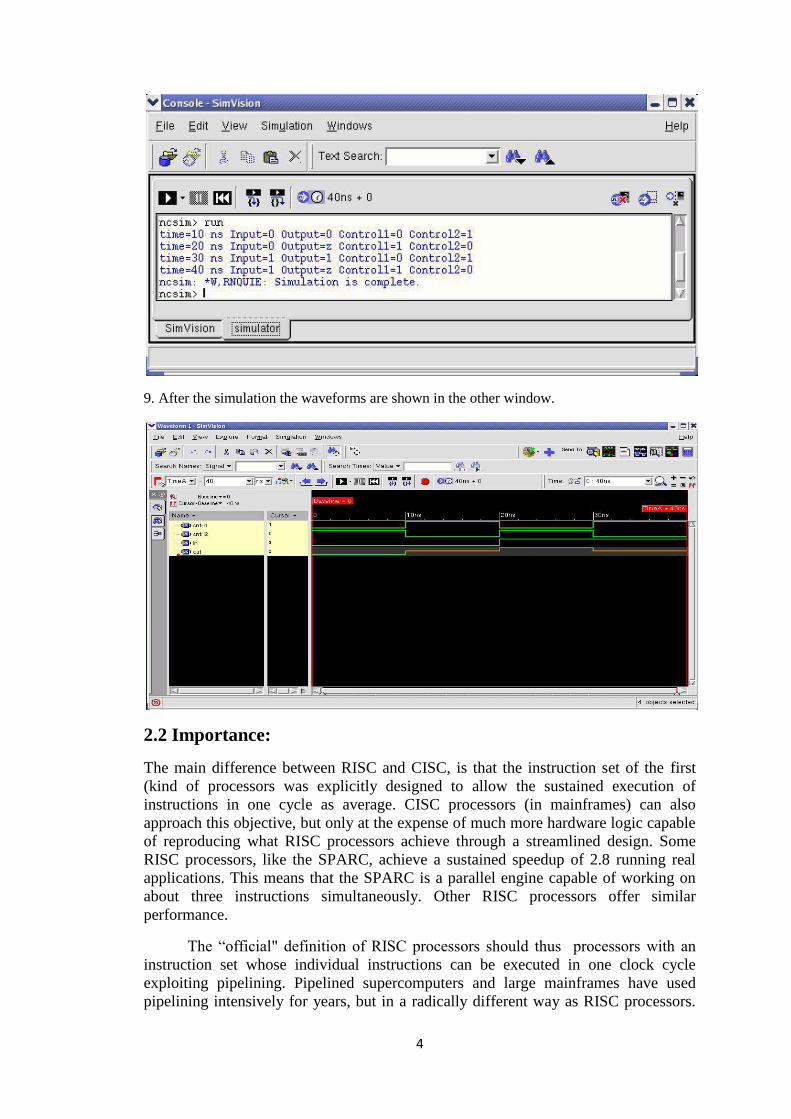
9. After the simulation the waveforms are shown in the other window.
2.2 Importance:
The main difference between RISC and CISC, is that the instruction set of the first
(kind of processors was explicitly designed to allow the sustained execution of
instructions in one cycle as average. CISC processors (in mainframes) can also
approach this objective, but only at the expense of much more hardware logic capable
of reproducing what RISC processors achieve through a streamlined design. Some
RISC processors, like the SPARC, achieve a sustained speedup of 2.8 running real
applications. This means that the SPARC is a parallel engine capable of working on
about three instructions simultaneously. Other RISC processors offer similar
performance.
The “official" definition of RISC processors should thus processors with an
instruction set whose individual instructions can be executed in one clock cycle
exploiting pipelining. Pipelined supercomputers and large mainframes have used
pipelining intensively for years, but in a radically different way as RISC processors.

5
In IBM mainframes, for example, the instruction set was given by "tradition” and
pipelining was implemented in spite of an instruction set which was not designed for
it. Of course there are ways to accommodate pipelining, but at a much higher cost.
This is the reason why other pipelined mainframes. Like the CDC/6600, are seen as
the precursors of RISC machines rather than the IBM/360 behemoths. In summary:
taking pipelining as the starting point it is easy to deduct all other features of RISC
processors.
Non-RISC design philosophy:
In the early days of the computer industry programming was done in
assembly language or machine code, which encouraged powerful and easy to use
instructions. CPU designers therefore tried to make instructions that would do as
much work as possible. With the advent of higher level languages, computers
architects also started to create dedicated instructions to directly implement, center in
Central mechanisms of such languages. Another general goal was to provide every
possible addressing mode for every instruction, known as orthogonality, to compiler
implementation. Arithmetic operations could therefore often have results as well as
operands directly in memory (in addition to register or immediate).
CPUs also had relatively few registers, for several reasons:
• More registers also implies more time consuming saving and restoring contents on
the machine stack.
• A large number of registers requires a large number of instruction bits as register
specifies. Meaning less dense code (see below)
• CPU registers are more expensive than external memory locations; large register
sets were cumbersome with limited circuit boards or chip integration.
RISC design philosophy:
In the mid 1970s researchers at IBM (am/ similar projects elsewhere)
demonstrated that the majority of combination, of these orthogonal addressing modes
and instructions were not used by most programs generated by compilers available at
the time. It proved difficult in many cases to write a compiler with more than limited
ability to take advantage of the features provided by conventional CPUs.
It was also discovered that, on micro coded implementations of
architectures, complex operations tended to be slower than a sequence of simpler
operations doing the same thing. This was in part an effect of the fact that many
designs were rushed, with little time to optimize or tune every instruction. But only
those used most often, as mentioned elsewhere, core memory had long since been
slower than many CPU designs. The advent of semiconductor memory reduced this
difference, but it was still apparent that more registers (and later caches) would allow
higher CPU operating frequencies. Additional registers would require sizable chip or
board areas which, at the time (1975), could be made available if the complexity the
CPU logic was reduced.
The clock rate of a CPU is limited by the time it takes to execute the
slowest sub-operation of any instruction; decreasing that cycle-lime often accelerates
the execution of other instruction. The focus on "reduced instructions" led to the

6
resulting machine being called a 'reduced instruction set computer" (RISC). The goal
was to make instructions so simple that they could easily be pipelined. In order
achieve a single clock throughput at high frequencies.
Instruction set size and alternative terminology:
A common misunderstanding of the phrase "reduced instruction set
computer" is the mistaken idea that instructions are simply eliminated, resulting in a
smaller set of instructions. In fact, over the years, RISC instruction sets have grown in
size, and today many of them have a larger set of instructions than many CISC CPUs.
Some RISC processors such as the INMOS Transputer have instruction sets as large
as,say,the CISC IBM System/370;and conversely, the DEC PDP-8 clearly a CISC
Cpu because many of its instructions involve multiple memory accesses - has only It
basic instructions, plus a few extended instructions.
The term "reduced" in that phrase was intended to describe the fact
that the amount of work any single instruction accomplishes is reduced at most a
single data memory cycle - compared to the “complex instructions “of CISC CPUs
that may require dozens of data memory cycles in order to execute a single
instruction”.
Typical characteristic of RISC:
For any given level of general performance, a RISC chip will typically haw far
fewer transistors dedicated to the core logic which originally allowed designer to
increase the size of the register set and increase internal parallelism. Other features,
which are typically found in RISC architectures, are
• Uniform instruction format. Using a single word with the OPCODE in the same bit
positions in every instruction, demanding less decoding.
• Identical general purpose registers. Allowing any register to be used in any context,
simplifying compiler design (although normally there are separate floating point
registers).
• Simple addressing modes. Complex addressing performed via sequences of
arithmetic and/or load-store operations
• Few data types in hardware some CISCs have byte string instructions, or support
complex numbers, this is so far unlikely to be found on a RISC.
Exceptions abound, of course, within both CISC and RISC.
RISC designs are also more likely to feature a Harvard memory
model, where the instruction stream and the data stream are conceptually separated;
this means that modifying the memory where code is held might not have any effect
on the instructions executed by the processor (because the CPU tins a separate
instruction and data cache), at least until a special synchronization instruction is
issued. On the upside, this allows both caches to be accessed simultaneously, which
can often improve performance.

7
RISC and x86:
However, despite many successes, RISC has made less inroads into the
desktop PC and commodity server markets, where Intel's x86 platform remains the
dominant processor architecture (Intel is facing increased competition from AMD,but
even AMD's processor implement the x86 platform, or a 64-bit superset known as
(x86-64).There are three main reasons for this.
1. The very large base of proprietary PC applications are written for x86, whereas no
RISC platform has a similar installed base, and this means PC users were locked into
the x86.
2. Although RISC was indeed able to scale up in performance quite quickly and
cheaply, Intel took advantage of its large market by spending vast amounts of money
on processor development. Intel could spend many times as much as any RISC
manufacturer on improving low level design and manufacturing.
3. Later, more powerful processors such as Intel P6 and AMD K6 had similar RISC-
like units that executed a stream of micro-operations generated from decoding wages
that split most x86 instructions into several pieces. Today, these principles have been
further refined and are used by modern x86 processors such as Intel Core 2 and AMD
K8. The first available chip deploying such techniques was the Next Gen Nx586
released in 1994 (while the AMD K5 was severely delayed and released in 1995).
Examining:
The simplest way to examine the advantages and disadvantages of RISC architecture
is by contrasting it with its predecessor. Complex instruction set computer
architecture.
Multiplying Two Numbers in Memory:
On the right is a diagram representing storage scheme for a generic computer.
The main memory is divided into locations numbered from (row) 1 :( column) 1 to
(row) 6:(column) 4. The execution unit is responsible for carrying out all
computations. However, the execution unit can only operate on data that has been
loaded into one of the six Registers (A,B,C,D,E or F).Let's say we want to find the
product of two numbers - one stored in Location 2:3 and another stored in location 5:2
and then store the product back in the location 2:3.

8
The CISC Approach:
The primacy goal of CISC architecture is to complete a task in as few lines of
assembly as possible. This is achieved by building processor hardware that is capable
of understanding and executing a series of operations. For this particular task a CISC
processor would come prepared with a specific instruction (we'll call it "MULT")
When executed, this instruction loads the two values into separate registers, the
operands in the execution unit, and then stores the product in the appropriate register.
Thus, the entire task of multiplying two numbers can be completed with one
instruction:
MULT 2:3, 5:2
MULT is what is known as a 'complex instruction". It operates directly on the
computer's memory banks and does not require the programmer to explicitly call any
loading or storing functions. It closely resembles a command in a higher level
language. For instance, if we let 'a' represent the value of 2:3 and "b" represent the
value of 5:2, then this command is identical to the C statement "a = a*b".
The RISC Approach:
RISC processors only use simple instructions that can be executed within
one clock cycle. Thus, the "MULT" command described above could be divided into
their separate commands "LOAD," which moves data from the memory bank to a
register, "PROD" which finds the product of two operands located within the
registers, and "STORE" which moves data from a register to the memory banks. In
order to perform the exact series of steps described in the CISC approach, a
programmer would need to code four lines of assembly:
LOAD A, 2:3
LOAD B, 5:2
PROD A, B
STORE 2:3, A
At first, this may seem like a much less efficient way of completing the
operation. Because there are more lines of code, more RAM is needed to store the
assembly level instruction. The compiler must perform more work to convert a high-
level language statement into code of this form.
CISC Emphasis on hardware whereas RISC emphasis on software. CISC
Includes multi-clock complex instructions and RISC includes single-clock, reduced
instruction only. Memory-Memory: "LOAD" and "STORE “are independent
instructions. Small code sizes, high cycles per second are in CISC and Low cycles per
second, large code sizes are there in the RISC. In CISC Transistors are used for
storing complex instructions and RISC spends more transistors on memory register.
Separating the "LOAD" and "STORE" instructions actually reduces the
amount of work that the computer must perform. After a CISC-style "MULT"
command is executed, the processor automatically erases the registers. If one of the
operands needs to be used for another computation, the processor must re-load the
data from the memory bank into a register. In RISC, the operand will remain in the
register until another value is loaded in its place.

9
The Performance Equation:
The following equation is commonly used for expressing a computer's performance
ability:
Time = time X cycles X instruction
Program cycle instruction program
The CISC approach attempts to minimize the number of
instructions per program, sacrificing the number of cycles per instruction. RISC does
the opposite, reducing the cycles per instruction at the cost of the number of
instructions per program.
RISC success stories:
RISC designs have led to a number of successful platforms and architectures, some of
larger ones being:
• ARM - The ARM architecture dominates the market for high performance, low
power, low cost embedded systems(typically 100-599MHz in 2008)ARM Ltd. which
licensed intellectual property rather than manufacturing chips, reported that 10 billion
licensed chips had been chipped as of early 2008. ARM is deployed in countless
mobile devices such as:
-Apple iPods (custom ARM7TDMI Soc)
-Apple iPhone (Saoune ARM1176JZFM
-Nintendo Game Boy Advance (ARM7TDMI)
-Nintendo DS (ARM7TDMI, ARM946E-S)
-Sony Network Walkman (Sony-in house ARM based chip)
-Some Nokia and Sony Ericsson mobile phones (often Symbian OS based devices)
• MIPS's MIPS line, found in most SGI computers and the Play station, play station
2, Nintendo 64(discontinued), play station Portable game consoles and residential
gateways like Linksys WRT54G series.
2.3 Organization of the report:
The report is organized in the following chapters:
Chapter 2 gives a brief introduction to VLSI and design flow of the VLSI.
Chapter 3 gives the brief introduction to Verilog HDL, key words, operations,
data types, modeling, loops and procedures used in the project code.
Chapter 4 gives the architecture of the project and it also describes the
architecture.
Chapter 5 gives the modules description, source code, code explanation,
waveforms and wave forms explanation of all individual‟s modules.
Chapter 6 presents the results (RTL, schematic diagrams of all modules and
synthesis reports).
Chapter 7 gives the advantage and disadvantages of the project.
Chapter 8 summarizes the project with a conclusion and discusses the thoughts
on the project.

10
2.4 Application areas:
The TX9956CXBG is the first standard 64bit microprocessor to employ the High-
performance TX99/H4 CPU Core and industry-leading 90nm process technology. The
TX9956CXBG device is the first standard 64b1t microprocessor to employ the high-
performance TX99/H4 CPU core and industry-leading 90nm process technology.
With 533 to 666Hz maximum operating frequency, the new TX9956CXBG is
currently the highest-performance microprocessor in the TX System RISC general-
purpose product line. It is targeted at diverse applications, including multifunction
printers and high-end set-top boxes .With the introduction, of the TX9956CXBG.
Toshiba continues to grow its bus-compatible, general-purpose microprocessor
portfolio to provide scalability and higher performance to customers.
2.5 Typical IC Design Flow:
Fig.2.1VLSIDesignFlow

11
Chapter 3
IMPLEMENTATION
3.1 Description:
The Architecture mainly consists of following units:
1. ALU unit
2. Memory unit
3. Control and Decoder unit
4. Program Counter unit
5. Instruction Register unit
6. Internal Register unit
7. Tristate Buffer unit
8. 64-bit 8:1 Multiplexer A & B unit
9. 6-bit 2:1 Multiplexer unit
10. Clock generator unit
When the clock generator generates the three clock cycles and gives
that three clock cycles to control and decoder unit. Then that unit will set LdIr port to
1 which means that it is telling to the instruction register to load the data from the
memory or internal register. After loading the data that data is given to program
counter and control and decoder unit. In the project the data will be 64-bit data. In that
data first 6 LSB bits are for memory address, last four MSB bits are for OPCODE,
next 3 MSB bits are for operand source address and the next 3 MSB bits are for
operand destination address. According to that addresses the control and decoder unit
will load the operands from the memory or internal registers at the time of loading

12
operand from the memory or internal registers at the of loading operand from the
memory it will set the ports MemRd to 1 and MemWr to 0 which means that memory
read operation is going on. The data will be loaded into MuxA. If we want to do any
ALU operation we need two operands already one operand is loaded into the MuxA
the other operand will also be loaded into the MuxB in the same way. At the time
selecting the internal registers the control and decoder unit will tell which register we
have to select using the operand source address. Then the outputs (data) from two
Multiplexers are loaded into the ALU unit where the execution of operation will be
done. At that time the control and decode unit will tell which operation we want to do
using OpCode.
After doing Alu operation that output can be stored in either internal
registers or memory. If we want to store the data in the internal registers then the
control and decoder unit will select the destination register using the operand
destination address. And if we want to store the data in the memory then the control
and decoder unit will set the MemWr to 1 and MemRd to 0 so that we can write the
data into the memory. For selecting the address to where we to store the data in the
memory it will use the memory address in the OpCode and if we want to use the
different address location, this address location will be selected by using 2:1 mux with
a fetch select line under the control and decoder unit. While storing the output data
from the Alu unit into the internal registers the buffer will be in high impedance state
which means that it will not allow the data to flow into the memory unit. And while
storing the output data into the memory the buffer will be set to 1 so that the data will
be loaded into the memory. The above process is repeated if we want to do another
Alu operation.
In the architecture there 11 modules and 1 top module. The modules are
1. ALU
2. Memory
3. Control and Decoder
4. Program Counter
5. Instruction Register
6. Internal Register
7. Tristate Buffer
8. 64-bit 8:1 Multiplexers(2)
9. 6-bit 2:1 Multiplexer
10. Clock generator

13
3.2Code Implementation:
Verilog HDL is one of the two common Hardware Description Languages (HDL)
used by integrated circuit (IC) designers. The other one is VHDL HDL's allows the
design cycle in order to correct errors or experiment with different architectures.
Designers described in HDL are technology-independent, easy to design and debug,
and are usually more readable than schematics, particular for large circuits.
3.3 ALU (Arithmetic and Logic Unit):
Fig. 5.1 ALU Block diagram
We design ALU which carry arithmetic operations are ADD, SUB, MUL, INR, and
DCR. Logical operations are AND, OR, XOR, LS, RS, INV and INV of Data. We
designed ALU with five inputs and one output, one input is from output MUXA
which is called OutA,2nd
input from MUXB called OutB, 3rd
input SelC is from
control & decoding module, this port gives OpCode to ALU, 4th
input is InClk and
finally 5th
is Reset. Outputs, AluOut carry out final result. Control & decoder section
selects the data to OutA and OutB, at the same time it will provide the ALU OpCode.
So that ALU collects the data from the two inputs OutA, OutB and do the operations
as per OpCode received and put the result in AluOut.
3.3.1 Algorithm:
1. Start
2. Inputs from Mux A and Mux B, Reset, SelC, and InClk
3. Output is AluOut
4. If negative edge of InClk and Reset
5. Then if SelC is 0000 no operation is allocated
6. If SelC is 0001 add OutA and outB and give result to AluOut
7. If SelC is 0010 subtract OutA with outB and give result to AluOut
8. If SelC is 0011 multiply OutA with outB and give result to AluOut
9. If SelC is 0100 increment OutA by one and give result to AluOut
10. If SelC is 0101 decrement OutA by one and give result to AluOut
11. If SelC is 0110 do and operation between OutA and outB and gives the result
to AluOut
12. If SelC is 1000 do EX-OR operation between OutA and outB and give the
result to AluOut
13. If SelC is 1001 do left shift OutA by 1 and give result to AluOut
14. If SelC is 1010 do right shift OutA by 1 and give result to AluOut
15. If SelC is 1011 pass OutA to AluOut
16. If SelC is 1100 complement OutA and give result to AluOut
OutA
OutB AluOut
Rst
InClk
SelC

14
17. If SelC is 1101 it is allocated to skip operation
18. If SelC is 1110 it is allocated to jump operation
19. If SelC is 1111 it is allocated to halt operation
20. If SelC is default pass OutA to AluOut
21. Stop
3.3.2 Code:
„timescale 1ns/1ps
module alu_1 (OutA, OutB, Rst, SelC, InClk, AluOut);
input Rst, InClk;
input [3:0] SelC;
input [63:0] OutA, OutB;
output reg [63:0] AluOut;
always @ (negedge InClk)
Begin
If (Rst == 1'b1)
Case (SelC)
//4'b0000:AluOut=default;
4'b0001: AluOut=OutA+OutB;
4'b0010: AluOut=OutA-OutB;
4'b0011: AluOut=OutA*OutB;
4'b0100: AluOut=OutA+1'b1;
4'b0101: AluOut=OutA-1'b1;
4'b0110: AluOut=OutA&OutB;
4'b0111: AluOut=OutA| OutB;
4'b1000: AluOut=OutA^OutB;
4'b1001: AluOut=OutA<<1;
4'b1010: AluOut=OutA>>1;
4'b1011: AluOut=OutA;
4'b1100: AluOut=~OutA;
endcase
end
endmodule
3.3.3 Code explanation:
As mention above ALU module collects two input data, one is OpCode and
one InClk and a reset. When InClk go to negative edge and Rst indicate low; then a
case statement is written as SelC (OpCode) as selection. This choice is given to a
specific OpCode (operation needs to perform) using the two input data‟s.
We left four choices for DEFALT, JMP, SKIP and HALT operations. We
assigned 0000 OpCode for DEFALT, 1101 is for SKIP, 1110 for JMP and 1111 for
HALT.

15
3.3.4 Waveforms:
Fig.5.2 ALU Waveforms
3.3.5 Waveform Explanation:
When clock is given, if Rst=1 and SelC is some OpCode then according to
that OpCode Alu will do corresponding operations, here 0001 is for addition. In the
above waveform we can see that OutA and outB is added and the result is stored in
AluOut.
3.4 Memory:
Fig.5.3 Memory Block diagram
In this module we have three inputs and one inout port. One input is Addr (address) of
the memory where we want to store the data. The other input is MemRd (Memory
read), when this input is one the data from the memory can be read. And the last input
is MemWr (Memory write), when this input is one the data can be write into the
memory. The inout port is used to store and load to and from the memory.
3.4.1 Algorithm:
1. Start
2. Inputs memory write, memory read and Addr.
3. Inout Databus.
4. Allocate a 64-bit register.
5. Assign a text data to the 64-bit register.
6. If memory write is 1 and memory read is 0 then register with Addr is assigned
to DataBus and output is high impedance.
7. Else memory write is 0 and memory read is 1 then assign DataBus output with
Addr of register and input is high impedance.
8. Else then DataBus is high impedance.
9. Stop.
Addr
MemRd DataBus
MemWr

16
3.4.2 Code
„timescale 1ns/1ps
module memory_1 (DataBus, MemWr, MemRd, Addr);
inout [63:0] DataBus;
input MemWr;
input MemRd;
input [5:0] Addr;
reg [63:0] datareg;
reg [63:0] Mem [0:63];
//initial $fread ("om.bin", Mem);
initial $readmemh ("om.txt", Mem);
always @ (MemWr or MemRd or Addr or datareg)
begin
if (MemWr==1'b1 && MemRd==1'b0)
begin
Mem [Addr] =DataBus;
datareg=64'hzzzzzzzzzzzzzzzz;
end
else if (MemWr==1'b0 && MemRd==1'b1)
datareg= Mem [Addr];
else
datareg=64'hzzzzzzzzzzzzzzzz;
end
assign DataBus = datareg;
endmodule
3.4.3 Code Explanation:
When the inputs MemWr==1’b1 and MemRd==1’b0 the data which is in the DataBus is loaded into the memory the specified address and if the inputs MemWr==1’b0 and MemRd==1’b1 the data from the memory is loaded into the datareg(internal register) after that it is loaded into the DataBus.
3.4.4 Waveforms:
Fig. 5.4 Memory waveforms

17
3.4.5 Waveform Explanation:
When MemWr=1, MemRd=0 and if Addr is given then the data in the
DataBus will be written in that memory location otherwise if MemWr=0, MemRd=1
and if Addr is given then the data in that Addr is given then that data in that address
location from the memory is given to DataBus. In the above waveform when
MemWr=0 and MemRd=1 then the data is given to DataBus as 1111111100000000
from memory.
3.5 Control and Decoder:
Fig. 5.5 Control & Decoder Block diagram In this module we have 7 inputs and 9 outputs. They are OpCode, OpDesAddr,
OpSrcAddr, Clk1, Clk2, Fetch, Rst, SelA, SelB, SelC, SelD, IncPc, LdIr, LdPc,
MemRd, and MemWr. According to the inputs of Clk1, Clk2 and fetch the other ports
are given corresponding inputs to do the required operation.
3.5.1 Algorithm:
1. Start.
2. Inputs clk1, clk2, fetch, OpCode, OpSrcAddr and OpDesAddr.
3. Outputs LdPc, IncPc, LdIr, MemRd, MemWr, SelA, SelB, SelC and SelD.
4. Parameter has to be assigned.
5. When reset is 0 and OpCode is 1111 then SelA is 000, SelB is 000, SelC is
0000, SelD is 000, LdPc is 0, IncPc is 0, LdIr is 0, MemRd is 0 and MemWr is
0.
6. If clk1 is 0, clk2 is 1 and fetch is 1 then SelA is 000, SelB is 000, SelC is
0000, SelD is 000, LdPc is 0, LdIr is 0, MemRd is 0, MemWr is 0.
7. If clk1 is 1, clk2 is 1, fetch is 1 then SelA is 000, SelB is 000, SelC is 0000,
SelD is 000, LdPc is 0, IncPc is 0, LdIr is 0, MemRd is 1, MemWr is 0.
8. If clk1 is 0, clk2 is 0, fetch is 1 then SelA is 000, SelB is 000, SelC is 0000,
SelD is 000, LdPc is 0, IncPc is 0, LdIr is 1, MemRd is 1, MemWr is 0.
9. If clk1 is 1, clk2 is 0, fetch is 1 then SelA is 000, SelB is 000, SelC is 0000,
SelD is 000, LdPc is 0, IncPc is 0, LdIr is 1, MemRd is 0, MemWr is 0.
10. If clk1 is 0, clk2 is 1, fetch is 0 then SelA is 000, SelB is 000, SelC is 0000,
SelD is 000, LdPc is 0, IncPc is 1, LdIr is 0, MemRd is 0, MemWr is 0.
OpCode SelA
OpDesAddr SelB
OpSrcAddr SelC
Clk1 SelD
Clk2 IncPc
Fetch LdIr
Rst LdPc
MemRd
MemWr

18
11. If clk1 is 1, clk2 is 1, fetch is 0 then SelA is 111, SelB is 000, SelC is 0000,
SelD is 000, LdPc is 0, IncPc is 0, LdIr is 0, MemRd is 1, MemWr is 0.
12. If clk 1 is 0, clk2 is 0, fetch is 0 then SelA is 111, SelB is 000, SelC is 0000,
SelD is 000, LdPc is 0, IncPc is 0, LdIr is 0, MemRd is 1, and MemWr is 0.
13. If clk1 is 1, clk2 is 0, fetch is 0 then SelA is 000, SelB is 000, SelC is 0000,
SelD is 000, LdPc is 0, IncPc is 0, LdIr is 0, MemRd is 0, and MemWr is 0.
14. Default is SelA is 000, SelB is 000, SelC is 0000, SelD is 000, LdPc is o,
IncPc is 0, LdIr is 0, MemRd is 0, and MemWr is 0.
15. Stop.
3.5.2 Code:
„timescale 1ns/1ps
module
controler1(Clk1,Clk2,Fetch,Rst,OpCode,OpSrcAddr,OpDesAddr,LdIr,Ldpc,Incpc,Me
mRd,MemWr, SelA, SelB b, SelC, SelD);
input Clk1, Clk2, Fetch, Rst; input [3:0] OpCode; input [2:0] OpSrcAddr,
OpDesAddr;
output reg LdIr, LdPc, IncPc, MemRd, MemWr;
output reg [2:0] SelA, SelB, SelD;
output reg [3:0] SelC;
parameter AddrSetUp1 =3'b011;
parameter InstrFetch =3'b111;
parameter InstrLoad =3'b001;
parameter Idle =3'b101;
parameter AddrSetUp2 =3'b010;
parameter OperandFetch =3'b110;
parameter AluOperation =3'b000;
parameter StoreResult =3'b100;
wire [2:0] Control;
assign Control={Clk1,Clk2,Fetch};
always @ (Control or Rst or OpCode or OpSrcAddr or OpDesAddr)
begin
if(Rst==1'b0 && OpCode==4'b1111)
begin
SelA =3'b000;
SelB =3'b000;
SelC =4'b0000;
SelD =3'b000;
LdPc =1'b0;
IncPc=1'b0;
LdIr =1'b0;
MemRd =1'b0;
MemWr =1'b0;
end
else
begin
case (Control)
AddrSetUp1: begin
SelA =3'b000;

19
SelB =3'b000;
SelC =4'b0000;
SelD =3'b000;
LdPc =1'b0;
IncPc =1'b0;
LdIr =1'b0;
MemRd =1'b0;
MemWr =1'b0;
end
InstrFetch: begin
SelA =3'b000;
SelB =3'b000;
SelC =4'b0000;
SelD =3'b000;
LdPc =1'b0;
LdIr =1'b0;
IncPc =1'b0;
MemRd =1'b1;
MemWr =1'b0;
end
InstrLoad: begin
SelA =3'b000;
SelB =3'b000;
SelC =4'b0000;
SelD =3'b000;
LdPc =1'b0;
IncPc =1'b0;
LdIr =1'b1;
MemRd =1'b1;
MemWr =1'b0;
end
Idle: begin
SelA =3'b000;
SelB =3'b000;
SelC =4'b0000;
SelD =3'b000;
LdPc =1'b0;
IncPc =1'b0;
LdIr =1'b1;
MemRd =1'b0;
MemWr =1'b0;
end
AddrSetUp2: begin
SelA =3'b000;
SelB =3'b000;
SelC =4'b0000;
SelD =3'b000;
LdPc =1'b0;
IncPc =1'b1;
LdIr =1'b0;

20
MemRd =1'b0;
MemWr =1'b0;
end
OperandFetch: begin
SelA =3'b111;
SelB =OpSrcAddr;
SelC =OpCode;
SelD =3'b000;
LdPc =1'b0;
IncPc =1'b0;
LdIr =1'b0;
MemRd =1'b1;
MemWr =1'b0;
end
AluOperation: begin
SelA =3'b111;
SelB =OpSrcAddr;
SelC =OpCode;
SelD =3'b000;
LdPc =1'b0;
IncPc =1'b0;
LdIr =1'b0;
MemRd =1'b1;
MemWr =1'b0;
end
StoreResult: begin
SelA =3'b000;
SelB =3'b000;
SelC=4'b0000;
SelD =OpSrcAddr;
LdPc =1'b0;
IncPc =1'b0;
LdIr =1'b1;
MemRd =1'b1;
MemWr =1'b0;
end
default: begin
SelA =3'b000;
SelB =3'b000;
SelC =4'b0000;
SelD =3'b000;
LdPc =1'b0;
IncPc =1'b0;
LdIr =1'b0;
MemRd =1'b0;
MemWr =1'b0;
end
endcase
end
end

21
endmodule
3.5.3 Code Explanation:
According to the inputs of control (Clk1, Clk2, Fetch) the corresponding
case is selected and the operation in that block is done. After 8 clocks cycle‟s one
ALU operation is done.
3.5.4 Waveforms:
Fig. 5.6 Control & Decoder Waveforms
3.5.2 Waveform Explanation:
According to Clk1, Cl2 and fetch the parameters will be given codes,
corresponding to that codes the LdPc, IncPc, LdIr, MemRd, MemWr, SelA, SelB,
SelC, SelD will change so that the given operation will be done.
3.6 Program Counter:
Fig. 5.7 Program Counter Block diagram
In this module we have 4 inputs and 1 output. The data where we want to store the
data is given to OpDesAddr and according to the inputs of IncPc, LdPc and Rst the
output is obtained.
3.6.1 Algorithm:
1. Start
2. Inputs Mem Addr, IncPc, Rst, LdPc.
3. Output PcOut.
MemAddr
IncPc Addr
LdIr
Rst

22
4. If positive edge of IncPc and negative edge of Rst.
5. Then if reset is 0 then PcOut is 0.
6. Else LdPc is 1 then PcOut is Mem Addr.
7. Else IncPc by one.
8. Stop.
3.6.2 Code:
„timescale 1ns/1ps
module pro_count (MemAddr, IncPc, LdPc, Rst, Pcout);
input [5:0] MemAddr; input IncPc, LdPc, Rst;
output [5:0] Pcout; reg [5:0] sreg;
assign Pcout = sreg [5:0];
always @(posedge IncPc or negedge Rst)
begin
if (Rst == 1'b0)
sreg = 6'b000000;
else if (LdPc == 1'b1)
begin
sreg = MemAddr;
end
else
sreg = sreg + 1;
end endmodule
3.6.3 Code Explanation:
If Rst is 0 then sreg (internal register) is set to 0 and if Rst is 1 and if LdPc
(Load program counter) is 1 then memory address is loaded into the sreg and if LdPc
is 0 then sreg is incremented.
3.6.4 Waveforms:
Fig. 5.8 Program Counter Waveforms
3.6.5 Waveform Explanation:
When Rst is 1 is given (here is a Clk) if LdPc is 1 then the MemAddr is
given to Pcout else if LdPc is 0 then the MemAddr is incremented. In the above

23
waveform when LdPc is 1, 11 from MemAddr is loaded into PcOut else if it is
incremented to 12, etc.
3.7 Instruction Register:
Fig.5.9 Instruction Register Block diagram
In this module we have 4 inputs and 4 outputs. According to the inputs of LdIr
(instruction register) and Clk the data from the DataBus is loaded into dreg (internal
register) or incremented. And if Reset is 0 then the data in the dreg is 0. The required
number of bits is given to the corresponding output ports like OpCode, OpDesAddr,
OpSrcAddr and MemAddr.
3.7.1 Algorithm:
1. Start.
2. Inputs Clk, Rst, LdIr, DataBus.
3. Output OpCode, OpDesAddr, OpSrcAddr, MemAddr.
4. Parameters OpCode is DataBus (63-60), OpSrcAddr is DataBus (59-57),
OpDesAddr (56-54) and MemAddr is DataBus (5-0) has to be assigned.
5. If Clk is positive edge and Rst is negative edge then if Rst is 0 then Databus is
zero.
6. Else if LdIr is 1 then DataBus is DataBus and if OpCode is 1101 then
increment MemAddr by one.
7. Else DataBus is DataBus.
8. Stop.
3.7.2 Code:
timescale 1ns/1ps
module m1 (DataBus, Clk, LdIr, Rst, OpCode, OpSrcAddr, OpDesAddr, MemAddr); input Clk; input Rst; input LdIr;
input [63:0] DataBus;
output [5:0] OpCode;
output [5:0] OpSrcAddr;;
output [5:0] OpDesAddr;
output [5:0] MemAddr;
reg [5:0] sreg;
assign OpCode=dreg [63:60];
assign OpSrcAddr=dreg [59:57];
assign OpDesAddr=dreg [56:54];
assign MemAddr=dreg [5:0];
always @ (posedge Clk or negedge Rst)
DataBus MemAddr
Clk OpCode
LdIr
OpSrcAddr
Rst
OpDesAddr

24
begin
if (Rst==1'b0)
dreg=64'h0000000000000000;
else if (LdIr==1'b1)
begin
dreg=DataBus;
if (dreg [63:60] =4'b1101)
dreg [5:0] =dreg [5:0] +1;
end
else
dreg=dreg;
end
endmodule
3.7.3 Code Explanation:
If Rst is 0 then dreg is 0. And if Rst is 1 and if LdIr is 1 then DataBus is
loaded into dreg or else dreg is unchanged. The last 4 bits (63:60) of DataBus is given
to OpCode, the 3 bits (59:57) is given to OpSrcAddr, the next 3 bits (56:54) are given
to OpDesAddr and the first 6 bits are given to (5:0) is given to MemAddr.
3.7.4 Waveforms:
Fig. 5.10 Instruction Register Waveforms
3.7.5 Waveform Explanation:
When Clk and Rst are given and if LdIr is 1 then the DataBus is given to
OpCode, OpSrcAddr, OpDesAddr and MemAddr to their bit length. In the above
waveform if LdIr is 1 then OpCode= B, OpSrcAddr=0, OpDesAddr=5 and
MemAddr=00.

25
3.8 Internal Registers:
Fig.5.11 Internal Register Block diagram
In this module we have 4 inputs and 6 outputs. Based on the input of SelD the output
of Alu (AluOut) is loaded into the dreg (internal register). And if reset is 0 then all the
registers are set to zero.
3.8.1 Algorithm:
1. Start
2. Input Clk, Rst, SelD, AluOut.
3. Output Reg1, Reg2, Reg3, Reg4, Reg5, Acc
4. Assign data registers to registers
5. If Clk is positive edge is negative edge then if reset is zero then Reg1=0, Reg2=0,
Reg3=0, Reg4=0, Reg5=0 and Acc=0
6. Else if Rst=1 and is SelD is 001then reg1=AluOut, if SelD is 010 then
reg2=AluOut, if SelD is 011then reg3=AluOut, if SelD is 100then reg4=AluOut, if
SelD is 101 then reg5=AluOut, if SelD is 110 then reg6=AluOut
7. Else default is reg1=reg1, reg2=reg2, reg3=reg3, reg4=reg4, reg5=reg5, reg6=reg6
8. Stop
3.8.2 Code:
„Timescale 1ns/1ps
module Program _Counter (Clk, Rst, SelD, AluOut, Reg1, Reg2, Reg3, Reg4, Reg5,
Acc);
input Clk;
input Rst;
input [2:0] SelD;
input [63:0] AluOut;
output [63:0] Reg1;
output [63:0] Reg2;
output [63:0] Reg3;
output [63:0] Reg4;
output [63:0] Reg5;
output [5:0] Acc;
reg [5:0] dreg1, dreg2, dreg3, dreg4, dreg5, dreg5;
AluOut Acc
SelD Reg1
Clk Reg2
Rst Reg3
Reg4
Reg5

26
assign Reg1=dreg1;
assign Reg2=dreg2;
assign Reg3=dreg3;
assign Reg4=dreg4;
assign Reg5=dreg5;
assign Acc=dreg6;
always @ (posedge Clk or negedge Rst or SelD)
begin
if (Rst==1'b0)
dreg1=64'h0000000000000000;
dreg2=64'h0000000000000000;
dreg3=64'h0000000000000000;
dreg4=64'h0000000000000000;
dreg5=64'h0000000000000000;
dreg6=64'h0000000000000000;
end
else
case (SelD)
3'b001:dreg1=AluOut;
3'b010:dreg2=AluOut;
3'b011:dreg3=AluOut;
3'b100:dreg4=AluOut;
3'b101:dreg5=AluOut;
3'b110:dreg6=AluOut;
default:
begin dreg1=dreg1;
dreg2=dreg2;
dreg3=dreg3;
dreg4=dreg4;
dreg5=dreg5;
dreg6=dreg6;
end
endcase
end
endmodule
else if (LdIr==1'b1)
begin
dreg=DataBus;
if (dreg [63:60] = 4'b1101)
dreg [5:0] = dreg [5:0] +1;
end
else
dreg=dreg;
end
endmodule
3.8.3 Code Explanation:
If Rst is 0 then all the registers are set to zero or else according to the
input of SelD the AluOut is loaded into the corresponding (based on SelD) register.

27
3.8.4 Waveforms:
Fig.5.12 Internal Register Waveforms
3.8.5 Waveforms Explanation: When Clk and Rst are given and if SelD then the corresponding register is
selected and the data in the AluOut is given to that register .In the waveforms SelD is
2 which means that the data in AluOut (AAAAAAAAAAAAAAAA) is given to
register2.
3.9 Tristate Buffer:
Fig.5.13 Tristate Buffer
In this module we have 4 inputs and 1 output. Here we use nor for giving input. The
neither inputs to that nor gate are Fetch, Clk2 and MemRd and the output is enabling.
If this enable is to set to 1 then the output from the Databus is AluOut.
3.9.1 Algorithm:
1. Start
2. Input fetches, Clk2, MemRd and AluOut
3. Output DataBus
4. Wire ena
5. The nor operation between fetch, clk2 and MemRd is assigned to ena
6. If ena is 1 then AluOut is assigned to Databus
7. Else high impedance
8. Stop
AluOut
Clk2 DataBus
Fetch
MemRd

28
3.9.2 Code:
„timescale 1ns/1ps
module buffer (fetch, clk2, MemRd, AluOut, Databus)
input fetch;
input clk2;
input MemRd;
wire ena;
input [63:0] AluOut;
output [63:0] Databus;
reg [63:0] Databus;
nor n1 (ena, fetch, clk2, MemRd);
always@ (AluOut or ena)
begin
if (ena==1'b1)
Databus=AluOut;
else
Databus=64'hzzzzzzzzzzzzzzzz;
end
endmodule
3.9.3 Code Explanation:
If the output from the nor gate (enable) is 1 then the data in the AluOut is
loaded into DataBus which means the output and if the enable is 0 then Databus
output is high independence state.
3.9.4 Waveforms:
Fig.5.14 Tristate buffer Waveforms
3.9.5 Waveforms Explanation:
When Clk2, Fetch and MemRd are given then the ena will be either 1 or 0.
If ena is 1 then the data in the AluOut is given to the Databus else Databus is in high
impedance state. In the above example ena=1 then the data in AluOut
(101010101010110) is given to the Databus.

29
4.0 64-bit 8:1 Multiplexers:
4.0.1 Multiplexer A:
Fig.5.15 Multiplexer. A Block diagram
In this module we have 8 inputs and 1 output. The inputs are internal
registers and one select line. Based on the select input corresponding register is
selected and the data which is in loaded into the output port (OutA).
Algorithm:
1. Start
2. Input Databus, reg1, reg2, reg3, reg4, reg5, Acc and SelA.
3. Output OutA.
4. If SelA is 001 OutA is assigned to reg1.
5. Else if SelA is 010 OutA is assigned to reg2.
6. Else if SelA is 011 OutA is assigned to reg3.
7. Else if SelA is 100 OutA is assigned to reg4.
8. Else if SelA is 101 OutA is assigned to reg 5.
9. Else if SelA is 110 OutA is assigned to Acc.
10. Else if SelA is 111 OutA is assigned to Databus.
11. Stop
Code:
module mux_a (Databus, reg1, reg2, reg3, reg4, reg5, acc, SelA, OutA);
input [63:0] Databus;
input [63:0] reg1;
input [63:0] reg2;
input [63:0] reg3;
Acc
Databus
Reg1 OutA
Reg2
Reg3
Reg4
Reg5
Reg6
SelA

30
input [63:0] reg4;
input [63:0] reg5;
input [63:0] acc;
input [2:0] SelA;
output [63:0] OutA;
reg [63:0] OutA;
always @ (SelA or Databus or reg1 or reg2 or reg3 or reg4 or reg5 or acc)
begin
case (SelA)
3'b001: OutA=reg1;
3'b010: OutA=reg2;
3'b011: OutA=reg3;
3'b100: OutA=reg4;
3'b101: OutA=reg5;
3'b110: OutA=acc;
3'b111: OutA=Databus;
default: OutA=64'hzz;
endcase
end
endmodule
Code Explanation:
Based on the select line the corresponding register is selected and the data in
the register is loaded into the output port (out A).And if the selection is not suited to
any one of the case then the output is high impedance state.
Waveforms Explanation: According to the selection of SelA the dreg in DatabuReg1, Reg2, Reg3,
Reg4, Reg5, Acc is given to OutA. In the above waveforms SelA=1 then the dreg1
(AAAAAAAAAAAAAAAAAA) is given to OutA.
Waveforms:
Fig.5.16 Multiplexer A Waveform
.

31
4.0.2 Multiplexer B:
Fig.5.17 Multiplexer B Block diagram
In this module we have 8 inputs and 1 output. The inputs are internal
registers and one select line. Based on the select input corresponding register is
selected and the dat which is in loaded into the output port (OutA).
Algorithm:
1. Start
2. Input Databus reg1, reg2, reg3, reg4, reg5, Acc and SelB.
3. Output outB.
4. If SelB is 001 outB is assigned to reg1.
5. Else if SelB is 010 outB is assigned to reg2.
6. Else if SelB is 011 outB is assigned to reg3.
7. Else if SelB is 100 outB is assigned to reg4.
8. Else if SelB is 101 outB is assigned to reg 5.
9. Else if SelB is 110 OutB is assigned to Acc.
10. Else if SelB is 111 OutB is assigned to Databus.
11. Stop
Code:
module muxb (databus, reg1, reg2, reg3, reg4, reg5, acc, SelA, OutB); input [63:0] Databus; input [63:0] reg1; input [63:0] reg2; input [63:0] reg3; input [63:0] reg4; input [63:0] reg5; input [63:0] acc; input [2:0] SelB;
Acc
Databus
Reg1 OutB
Reg2
Reg3
Reg4
Reg5
Reg6
SelB

32
output [63:0] OutB; reg [63:0] OutB;
always@ (SelB or Databus or reg1 or reg2 or reg3 or reg4 or reg5 or acc)
begin
case (SelB)
3'b001: outB=reg1;
3'b010: outB=reg2;
3'b011: outB=reg3;
3'b100: outB=reg4;
3'b101: outB=reg5;
3'b110: outB=acc;
3'b111: outB=Databus;
default: outB=64'hzz;
endcase
end
endmodule
Code Explanation:
Based on the select line the corresponding register is selected and the data in
the register is loaded into the output port (out B).And if the selection is not suited to
any one of the case then the output is high impedance state.
Waveforms:
Fig.5.17 Multiplexer B Waveforms
Waveforms Explanation:
According to the selection of SelB the data in Databus Reg1, Reg2, Reg3,
Reg4, Reg5, Acc is given to OutB. In the above waveforms SelB=1 then the data in
reg1 (BBBBBBBBBBBBBBBBBB) is given to outB.

33
4.1 6-bit 2:1 Multiplexer:
Fig.5.19 Multiplexer Block diagram
In this module we have 3 inputs and 1 output. Based on the input of Fetch output is
depended. The two possible outputs from this module are either MemAddr or PcOut.
4.1.1 Algorithm:
1. Start
2. Inputs MemAddr, PcOut and Fetch
3. Output Addr
If Fetch is 0 then Addr is MemAddr
5. Else Addr is PcOut
6. Stop
4.1.2 Code:
'timescale 1ns/1ps
module mux (MemAddr, PcOut, fetch, Addr);
input [5:0] MemAddr;
input [5:0] Pcout;
input fetch;
output [5:0] Addr;
reg [5:0] Addr;
always@ (fetch or Pcout or MemAddr)
begin
if (fetch==1'b0)
Addr=MemAddr;
else
Addr=PcOut;
end
endmodule
4.1.3 Code Explanation:
If the input Fetch is set to 0 then the output from the port Addr is MemAddr
and if the input Fetch is set to 1 then the output from the port Addr is PcOut.
MemAddr
Addr
Fetch
PcOut

34
4.1.4 Waveforms:
Fig.5.20 Multiplexer Waveform
4.1.5 Waveform Explanation:
According to the selection of Fetch the data in MemAddr and PcOut is given
to Addr. In the above waveforms Fetch=1 then the data in PcOut (01) is given as
Addr.
4.2 Clock Generator:
Fig.5.21 Clock Generator Block Diagram
In this module we have 2 inputs and 3 outputs. Based on the rising edge of the Clk
and Rst the outputs clk1, clk2, fetch are generated.
4.2.1 Algorithm:
1. Start
2. Inputs Clk and Rst.
3. Output clk1, clk2 and fetch
4. If Rst=0 then clk1, clk2, fetch=0
5. Else Clk is assigned clk1
6. If Clk negative edge then clk2 is complement of its state.
7. If clk2 negative edge then Fetch is complement of its state.
8. Stop
4.2.2 Code:
'timescale 1ns/1ps
module clkgen (clk, Rst, clk1, clk2, fetch);
input Clk, Rst;
Clk Clk1
Clk2
Rst
Fetch

35
output clk1;
output clk2;
output fetch;
reg clk1, clk2;
always @ (Clk)
begin
if (Rst==1'b0)
Clk=1'b0;
else
clk1=Clk;
end
always @ (negedge clk1 or negedge Rst)
begin
if (Rst==1'b0)
clk2=1'b0;
else
clk2=~clk2;
end
always@ (posedge clk2 or negedge Rst)
begin
if (Rst==1'b0)
fetch=1'b0;
else
fetch=~fetch;
end
endmodule
4.2.3 Code Explanation:
Based on this rising edge of the Clk if Rst is 0 then clk1 is 0 or else if Rst
is 1 then the clk1 is same as Clk. Based on the negative edge of clk1 and Rst if Rst is
0 then clk2 is 0 and if Rst is clk2 is negation of clk2. And based on the positive edge
of clk2 and negative edge of Rst if Rst is 0 then fetch is 0 and if Rst is 1 output fetch
is negation of fetch.
4.2.4 Waveforms:
Fig.5.22 Clock Generator Waveforms

36
4.2.5 Waveforms Explanation:
According to Clk and Rst then ck1, clk2 and fetch are generated. In the
above example when Clk and Rst are 1 then clk1=clk, clk2=1 and fetch is 0.
4.3 Top Module:
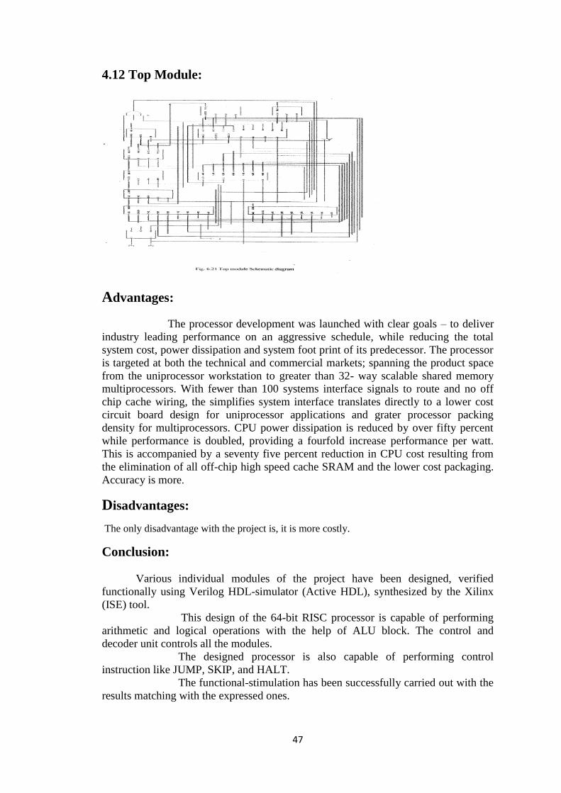
Fig. 5.23 Top Module Block diagram
In this module only two inputs will be there. The output is data which can be
stored in either memory or internal register. And if we want to take the data from the
memory or internal register data is used as input which means that the data (output) is
used as both input and output. So there is no particular for this module.
4.3.1 Algorithm:
1. Start
2. Inputs Clk, Rst
3. Declare all the inputs and outputs of all individual modules as wires.
4. Create objects for all modules.
5. Stop.
4.3.2 Code:
„Timescale 1ns/1ps
Module topmod_1 (Clk, Rst);
Input Clk, Rst;
Wire Clk1,Clk2,Fetch,Rst,LdIr,Ldpc,Incpc,MemRd,MemWr,InClk;
Wire [2:0] OpSrcAddr, OpDesAddr, SelA, SelB, SelD;
Wire [3:0] OpCode, SelC;
Wire [5:0] MemAddr, Pcout, Addr;
wire [63:0] DataBus,Acc,Reg1,Reg2,Reg3,Reg4,Reg5,AluOut,Data,Outa,Outb;
inst_reg om1 (DataBus, Clk, LdIr, Rst, MemAddr, OpCode, OpDesAddr,
OpSrcAddr);
pro_count om2 (MemAddr, IncPc, LdPc, Rst, Pcout);
mux_2x1 om3 (MemAddr, Pcout, Fetch, Addr);
mux_a om4 (DataBus, Reg1, Reg2, Reg3, Reg4, Reg5, Acc, SelA, OutA);
mux_b om5 (DataBus, Reg1, Reg2, Reg3, Reg4, Reg5, Acc, SelB, OutB);
alu_1 om6 (OutA, OutB, Rst, SelC, InClk, AluOut);
Clk om7 (Clk, Rst, Clk1, Clk2, Fetch);
tri12 om8 (Fetch, Clk2, MemRd, AluOut, DataBus);
memory_1 om9 (DataBus, MemWr, MemRd, Addr);
controller1
om1(Clk1,Clk2,Fetch,Rst,OpCode,OpSrcAddr,OpDesAddr,LdIr,Ldpc,Incpc,MemRd,
MemWr, SelA, SelB, SelC, SelD)
internal_reg_1 om12 (Clk, Rst, SelD, AluOut, Reg1, Reg2, Reg3, Reg4, Reg5, Acc);
Clk
Rst

37
or1 om13 (Clk1, Clk2, Fetch, InClk);
nor1 om14 (Fetch, Clk2, MemRd, ena); endmodule
4.3.3 Code Explanation:
In this module all the other modules objects are created. While compiling all
the modules is executed concurrently and in the last output waveforms are generated.
4.3.4 Waveforms:
Fig. 5.24 Top module waveform (1) 500ns
Fig. 5.24 Top module waveform (1) 500ns

38
Fig 5.25 Top module waveforms (2) 4000ns
Fig 5.25 Top module waveforms (2) 4000ns
4.3.5 Waveforms Explanation:
When Clk and Rst are given all the modules are instantiated and the
corresponding module will be executed and finally the result will be given to either
internal registers or memory.

39
4.4 Operation:
If we want to do any operation first we have type the instruction commands
and inputs in a text file and that file has to be stored in the memory and that text file
path has to be given in the top module code. The top module will go that path and
takes the commands in that file. For example take the file which we have stored in the
memory.
B280000000000001 //insert DataBus to Reg2
2222222222222222
B240000000000003 //insert DataBus to Reg1
1111111111111111
14C0000000000005 //add DataBus & Reg2, save in Reg3
1111111111111111
2300000000000007 //Sub DataBus, Reg1 save in Reg4
5555555555555555
3540000000000009 //Multiple DataBus, Reg1 save in Reg5
6666666666666666
424000000000000b //inc DataBus save in Reg1
1111111111111111
528000000000000d //dec DataBus save in Reg2
2222222222222222
670000000000000f //and Reg3, DataBus save in Reg4
2222222222222222
7740000000000011 // or Reg3, DataBus save in Reg5
CCCCCCCCCCCCCCCC
8280000000000013 // xor Reg1, DataBus save in Reg2
5555555555555555
9040000000000015 //leftshift DataBus save on Reg1
1111111111111111
A080000000000017 //rightshift DataBus save on Reg2
1111111111111111
C0C0000000000019 //complement of DataBus save in Reg3
1111111100000000
D00000000000001B //skip
1111111111111111
B28000000000001D //insert DataBus to Reg2
2222222222222222
E000000000000001
0000000000000000
1111111111111111
B280000000000022 //insert DataBus to Reg2
1111111111110000 The first command is b280000000000001 (hexadecimal) the binary code for that is 101100101000000000000000000000000000000000000000000000000000001; this code is used for storing the data (2222222222222222) in register2. Next command is b240000000000003 (hexadecimal) the binary code for that are 101100100100000000000000000000000000000000000000000000000000011; this code is used for storing the data (1111111111111111) in register 1. If we want to do Alu operation for example take addition the command will be 14c000000000005 (hexadecimal) the binary code for that is

40
000101100110000000000000000000000000000000000000000000000000101, in that first four MSB bits (0001) are for OPCODE. Here we took 0001 for addition. Next 3 MSB bits (010) is source address which means one of the operand is in that location, here it is register 2. And next 3 MSB bits (001) is destination address to where the result has to be stored, here in register 3 and we have to give another operand i.e., 1111111111111111 the other is which in register 2. After executing the addition operator the ALU module will sent the result (3333333333333333) to register 3 to store.
Now if we want to do another operation the above processes is repeated
of course the instruction command and input will change.

41
Chapter 4
SCHEMATIC RESULTS
4.1 ALU

42
4.2 Memory

43

44
4.3 Control and decoder
4.4 Program counter
4.5 Instruction Register:

45
4.6 Internal Register
4.7 Tristate Buffer
4.8 Multiplexer A:

46
4.9 Multiplexer B:
4.10 Multiplexer:
4.11 Clock Generator:
47
4.12 Top Module:
Advantages:
The processor development was launched with clear goals – to deliver
industry leading performance on an aggressive schedule, while reducing the total
system cost, power dissipation and system foot print of its predecessor. The processor
is targeted at both the technical and commercial markets; spanning the product space
from the uniprocessor workstation to greater than 32- way scalable shared memory
multiprocessors. With fewer than 100 systems interface signals to route and no off
chip cache wiring, the simplifies system interface translates directly to a lower cost
circuit board design for uniprocessor applications and grater processor packing
density for multiprocessors. CPU power dissipation is reduced by over fifty percent
while performance is doubled, providing a fourfold increase performance per watt.
This is accompanied by a seventy five percent reduction in CPU cost resulting from
the elimination of all off-chip high speed cache SRAM and the lower cost packaging.
Accuracy is more.
Disadvantages:
The only disadvantage with the project is, it is more costly.
Conclusion:
Various individual modules of the project have been designed, verified
functionally using Verilog HDL-simulator (Active HDL), synthesized by the Xilinx
(ISE) tool.
This design of the 64-bit RISC processor is capable of performing
arithmetic and logical operations with the help of ALU block. The control and
decoder unit controls all the modules.
The designed processor is also capable of performing control
instruction like JUMP, SKIP, and HALT.
The functional-stimulation has been successfully carried out with the
results matching with the expressed ones.

48
The design has been synthesized using FPGA technology from
Xilinx. This design has targeted the device family spartan3, device xc2s15. Package
cs144 and speed grade -6. This device belongs to the Virtex-E group of FPGA‟s from
Xilinx ,reducing or simplifying the instruction set was not the primary goal of RISC
architecture, it is pleasant side effect of techniques used to gain the highest
performance possible from the available technology.
Future scope:
We can extend this 64-bit RISC processor to 128-bit RISC processor by
changing the instruction format length and also by increasing more no. of registers we
can increase the memory of the processor. We can also include more(less compared to
CISC) no. of instruction so that we can do more no. of ALU operations.
References:
Moris Mano, Digital Design, PHI, 2007
Nicholas P.Carter, Schaum‟s Outline of Computer Architecture, 2002 p.96 ISBN
007136207X
J.Bhaskar, VHDL Primer.