Embed Size (px)
Citation preview
8/2/2019 CD 00267919
http://slidepdf.com/reader/full/cd-00267919 1/17
April 2011 Doc ID 17251 Rev 2 1/17
AN3176Application note
Designing notebook computer multimedia boards with capacitive
S-Touch ® controllers STMPE16M31 and STMPE24M31
Introduction
Multimedia boards in notebook computers typically require touchkeys, a slider for volumecontrol, and LEDs for backlighting. The S-Touch ® capacitive touchkey controllersSTMPE16M31 and STMPE24M31 are ideal for a multimedia board design due to their highversatility and various built-in intelligent features.
Multimedia PCBs are long and narrow, and routing the sensors to obtain optimalperformance is a challenge. This application note provides guidelines for a 4-layer PCB
design.
Figure 1. Example: multimedia board for a notebook application
www.st.com

8/2/2019 CD 00267919
http://slidepdf.com/reader/full/cd-00267919 2/17
Contents AN3176
2/17 Doc ID 17251 Rev 2
Contents
1 Definition of board requirements . . . . . . . . . . . . . . . . . . . . . . . . . . . . . . . 4
2 Layer stack up: 4-layer . . . . . . . . . . . . . . . . . . . . . . . . . . . . . . . . . . . . . . . 5
2.1 Routing . . . . . . . . . . . . . . . . . . . . . . . . . . . . . . . . . . . . . . . . . . . . . . . . . . . . 6
2.2 Ground plane . . . . . . . . . . . . . . . . . . . . . . . . . . . . . . . . . . . . . . . . . . . . . . . 7
2.3 Noise filtering to improve stability . . . . . . . . . . . . . . . . . . . . . . . . . . . . . . . . 8
3 Sensor design . . . . . . . . . . . . . . . . . . . . . . . . . . . . . . . . . . . . . . . . . . . . . . 9
3.1 Touchkey design . . . . . . . . . . . . . . . . . . . . . . . . . . . . . . . . . . . . . . . . . . . . . 9
3.2 Slider/wheel design . . . . . . . . . . . . . . . . . . . . . . . . . . . . . . . . . . . . . . . . . . 9
Appendix A Reference schematic diagram . . . . . . . . . . . . . . . . . . . . . . . . . . . . . 11
Appendix B Reference PCB layout of 4-layer multimedia board . . . . . . . . . . . . 12
Appendix C Reference dimensions for slider and touchkey for multimedia . . . .board. . . . . . . . . . . . . . . . . . . . . . . . . . . . . . . . . . . . . . . . . . . . . . . . . . 14
Appendix D Bill of material . . . . . . . . . . . . . . . . . . . . . . . . . . . . . . . . . . . . . . . . . . 15
Revision history . . . . . . . . . . . . . . . . . . . . . . . . . . . . . . . . . . . . . . . . . . . . . . . . . . . . 16
8/2/2019 CD 00267919
http://slidepdf.com/reader/full/cd-00267919 3/17
AN3176 List of figures
Doc ID 17251 Rev 2 3/17
List of figures
Figure 1. Example: multimedia board for a notebook application . . . . . . . . . . . . . . . . . . . . . . . . . . . . 1Figure 2. Cross-section of a typical PCB . . . . . . . . . . . . . . . . . . . . . . . . . . . . . . . . . . . . . . . . . . . . . . . 5Figure 3. Recommendation for 4-layer PCB routing . . . . . . . . . . . . . . . . . . . . . . . . . . . . . . . . . . . . . . 5Figure 4. Top layer sensor pad design . . . . . . . . . . . . . . . . . . . . . . . . . . . . . . . . . . . . . . . . . . . . . . . . 6Figure 5. Recommended routing for PWM/I2C signals and sensor traces. . . . . . . . . . . . . . . . . . . . . . 7Figure 6. Effect of GND plane on sensitivity . . . . . . . . . . . . . . . . . . . . . . . . . . . . . . . . . . . . . . . . . . . . 7Figure 7. Ground mesh . . . . . . . . . . . . . . . . . . . . . . . . . . . . . . . . . . . . . . . . . . . . . . . . . . . . . . . . . . . . 8Figure 8. Effect of overlay on sensitivity measured with a 10 mm diameter touchkey. . . . . . . . . . . . . 8Figure 9. Pseudo-position wheel/slider . . . . . . . . . . . . . . . . . . . . . . . . . . . . . . . . . . . . . . . . . . . . . . . . 9Figure 10. Ratiometric slider/wheel . . . . . . . . . . . . . . . . . . . . . . . . . . . . . . . . . . . . . . . . . . . . . . . . . . . 10Figure 11. Slider and device placement on a multimedia board . . . . . . . . . . . . . . . . . . . . . . . . . . . . . 10Figure 12. Reference schematic diagram . . . . . . . . . . . . . . . . . . . . . . . . . . . . . . . . . . . . . . . . . . . . . . 11Figure 13. Multimedia board for a notebook application . . . . . . . . . . . . . . . . . . . . . . . . . . . . . . . . . . . 12
Figure 14. PCB layout of multimedia board - top layer (sensor pads with GND mesh) . . . . . . . . . . . . 12Figure 15. PCB layout of multimedia board - mid layer 1 (no routing except for one short 3.3 V
trace). . . . . . . . . . . . . . . . . . . . . . . . . . . . . . . . . . . . . . . . . . . . . . . . . . . . . . . . . . . . . . . . . . 12Figure 16. PCB layout of multimedia board - mid layer 2 (with all the sensor traces and a small mesh
GND plane) . . . . . . . . . . . . . . . . . . . . . . . . . . . . . . . . . . . . . . . . . . . . . . . . . . . . . . . . . . . . 12Figure 17. PCB layout of multimedia board - bottom layer (all I2C traces, PWM traces and non-sensor
routing with a GND mesh) . . . . . . . . . . . . . . . . . . . . . . . . . . . . . . . . . . . . . . . . . . . . . . . . . 13Figure 18. Slider design on top layer . . . . . . . . . . . . . . . . . . . . . . . . . . . . . . . . . . . . . . . . . . . . . . . . . . 14Figure 19. Touchkey design with LED opening (reverse-mount LEDs) . . . . . . . . . . . . . . . . . . . . . . . . 14

8/2/2019 CD 00267919
http://slidepdf.com/reader/full/cd-00267919 4/17
Definition of board requirements AN3176
4/17 Doc ID 17251 Rev 2
1 Definition of board requirements
The following requirements should be defined before starting the design of the board:
1. The number of touchkeys
2. Slider or rotator implementation and number of sensor channels to be used for each
3. LED configuration and number of GPIOs needed to drive the LEDs
4. The power supply requirement (3.3 V or 5 V)
5. Signal connection to host
6. Module form factor
7. System considerations, such as overlay thickness, proximity to periodic noise source,etc.
8/2/2019 CD 00267919
http://slidepdf.com/reader/full/cd-00267919 5/17
AN3176 Layer stack up: 4-layer
Doc ID 17251 Rev 2 5/17
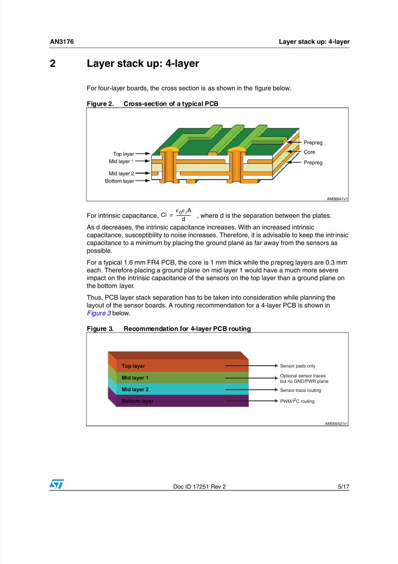
2 Layer stack up: 4-layer
For four-layer boards, the cross section is as shown in the figure below.
Figure 2. Cross-section of a typical PCB
For intrinsic capacitance, , where d is the separation between the plates.
As d decreases, the intrinsic capacitance increases. With an increased intrinsiccapacitance, susceptibility to noise increases. Therefore, it is advisable to keep the intrinsiccapacitance to a minimum by placing the ground plane as far away from the sensors aspossible.
For a typical 1.6 mm FR4 PCB, the core is 1 mm thick while the prepreg layers are 0.3 mmeach. Therefore placing a ground plane on mid layer 1 would have a much more severeimpact on the intrinsic capacitance of the sensors on the top layer than a ground plane onthe bottom layer.
Thus, PCB layer stack separation has to be taken into consideration while planning thelayout of the sensor boards. A routing recommendation for a 4-layer PCB is shown inFigure 3 below.
Figure 3. Recommendation for 4-layer PCB routing
Top layer
Mid layer 2
Mid layer 1
Prepreg
Bottom layer
Core
Prepreg
AM06641v1
Ciε0ε rA
d---------------=
Bottom layer
Mid layer 2
Mid layer 1
Top layer Sensor pads only
Optional sensor traces
but no GND/PWR plane
Sensor trace routing
PWM/I2C routing
AM066421v1
8/2/2019 CD 00267919
http://slidepdf.com/reader/full/cd-00267919 6/17
Layer stack up: 4-layer AN3176
6/17 Doc ID 17251 Rev 2
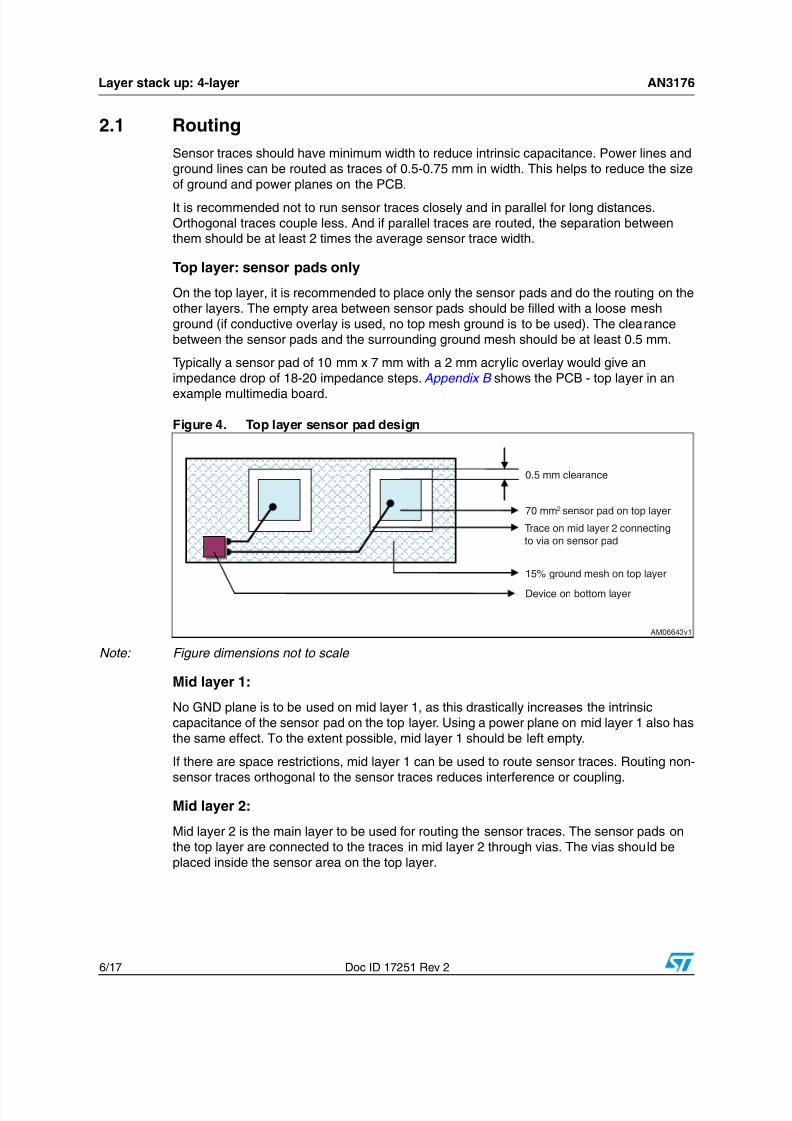
2.1 Routing
Sensor traces should have minimum width to reduce intrinsic capacitance. Power lines andground lines can be routed as traces of 0.5-0.75 mm in width. This helps to reduce the sizeof ground and power planes on the PCB.
It is recommended not to run sensor traces closely and in parallel for long distances.Orthogonal traces couple less. And if parallel traces are routed, the separation betweenthem should be at least 2 times the average sensor trace width.
Top layer: sensor pads only
On the top layer, it is recommended to place only the sensor pads and do the routing on theother layers. The empty area between sensor pads should be filled with a loose meshground (if conductive overlay is used, no top mesh ground is to be used). The clearancebetween the sensor pads and the surrounding ground mesh should be at least 0.5 mm.
Typically a sensor pad of 10 mm x 7 mm with a 2 mm acrylic overlay would give an
impedance drop of 18-20 impedance steps. Appendix B shows the PCB - top layer in anexample multimedia board.
Figure 4. Top layer sensor pad design
Note: Figure dimensions not to scale
Mid layer 1:
No GND plane is to be used on mid layer 1, as this drastically increases the intrinsiccapacitance of the sensor pad on the top layer. Using a power plane on mid layer 1 also hasthe same effect. To the extent possible, mid layer 1 should be left empty.
If there are space restrictions, mid layer 1 can be used to route sensor traces. Routing non-sensor traces orthogonal to the sensor traces reduces interference or coupling.
Mid layer 2:
Mid layer 2 is the main layer to be used for routing the sensor traces. The sensor pads onthe top layer are connected to the traces in mid layer 2 through vias. The vias should beplaced inside the sensor area on the top layer.
0.5 mm clearance
70 mm2 sensor pad on top layer
15% ground mesh on top layer
Device on bottom layer
Trace on mid layer 2 connecting
to via on sensor pad
AM06643v1

8/2/2019 CD 00267919
http://slidepdf.com/reader/full/cd-00267919 7/17
AN3176 Layer stack up: 4-layer
Doc ID 17251 Rev 2 7/17
Bottom layer:
All communication signals, such as the I2C or SPI, and asynchronous switching signals likethe RST and INT should be routed away from the sensor signals as the fast rise and falltimes of these signals affect the sensor measurement.
A good practice would be to route the sensor traces at the top portion of the PCB and assignthe bottom portion for routing I2C and GPIO signals, as shown in Figure 5 . This separatesthe two signal groups by the width of the PCB.
Figure 5. Recommended routing for PWM/I2C signals and sensor traces
Routing switching signals in the bottom layer is advisable for two reasons:
1. The bottom layer has a ground mesh to reduce noise, which helps to suppress thenoise coupled from the switching signals.
2. The switching signals are separated from the top layer by a large core and the midlayers. This reduces the interference of the switching signals on the sensor signals.
2.2 Ground planeThe ground plane in capacitive sensor applications impact performance in two ways:
1. The intrinsic capacitance of the sensors is increased.
2. The increased coupling of the electric field to GND causes a reduction in touchsensitivity.
Figure 6. Effect of GND plane on sensitivity
AM06644v1
Sensor traces at thetop of the PCB
I2C and PWM signals atthe bottom of the PCB
Device on thebottom layer
8/2/2019 CD 00267919
http://slidepdf.com/reader/full/cd-00267919 8/17
Layer stack up: 4-layer AN3176
8/17 Doc ID 17251 Rev 2
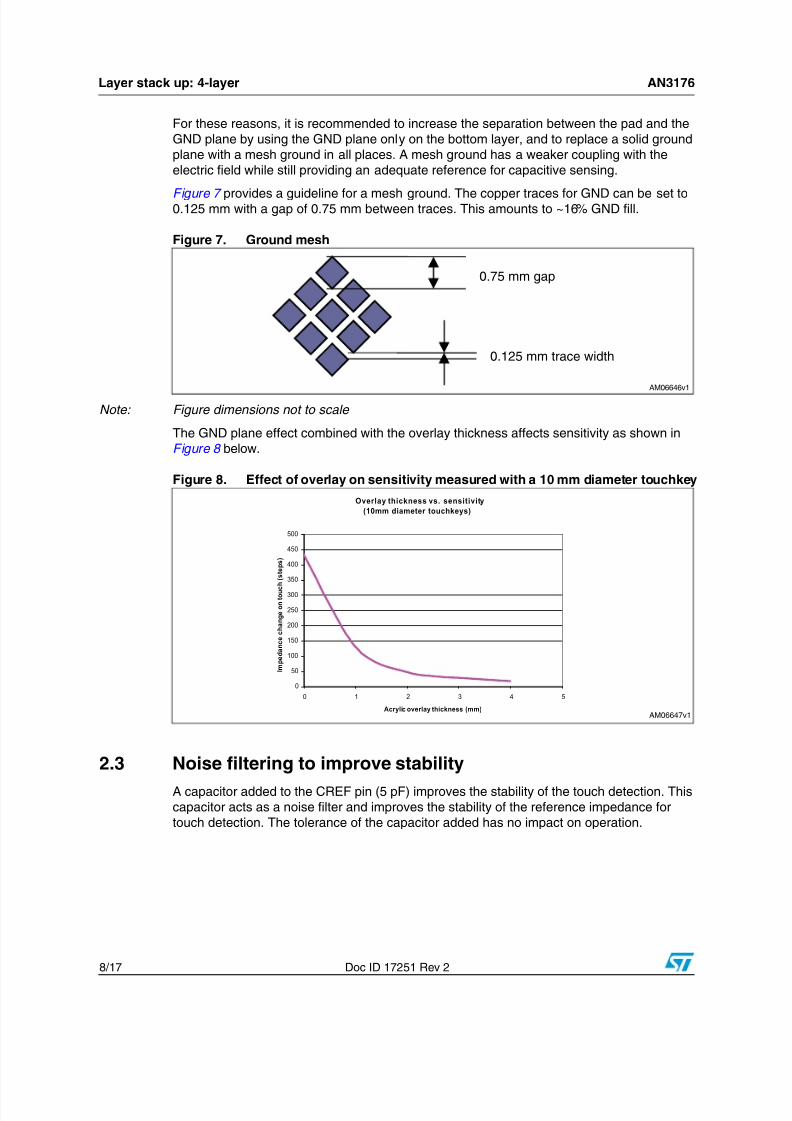
For these reasons, it is recommended to increase the separation between the pad and theGND plane by using the GND plane only on the bottom layer, and to replace a solid groundplane with a mesh ground in all places. A mesh ground has a weaker coupling with theelectric field while still providing an adequate reference for capacitive sensing.
Figure 7 provides a guideline for a mesh ground. The copper traces for GND can be set to0.125 mm with a gap of 0.75 mm between traces. This amounts to ~16% GND fill.
Figure 7. Ground mesh
Note: Figure dimensions not to scale
The GND plane effect combined with the overlay thickness affects sensitivity as shown inFigure 8 below.
Figure 8. Effect of overlay on sensitivity measured with a 10 mm diameter touchkey
2.3 Noise filtering to improve stabilityA capacitor added to the CREF pin (5 pF) improves the stability of the touch detection. Thiscapacitor acts as a noise filter and improves the stability of the reference impedance fortouch detection. The tolerance of the capacitor added has no impact on operation.
Overlay thickness vs. sensitivity
(10mm diameter touchkeys)
0
50
100
150
200
250
300
350
400
450
500
0 1 2 3 4 5
Acrylic overlay thickness (mm)
I m p e d a n c e c h a n g e o n t o u c h ( s
t e p s )

8/2/2019 CD 00267919
http://slidepdf.com/reader/full/cd-00267919 9/17
AN3176 Sensor design
Doc ID 17251 Rev 2 9/17
3 Sensor design
3.1 Touchkey design
Touchkeys can be of many shapes and sizes depending on the application. The thickness ofthe overlay and overlay material are the main factors that influence the sensor size indesigns. The larger the sensor area, the better the sensitivity to touch. It is recommended toensure a 0.5 mm clearance to the surrounding GND plane on the top layer.
LEDs are mounted on the bottom layer to illuminate when a touch event is detected in manyapplications. This can be achieved with reverse-mount LEDs on the bottom layer with a viahole opening in the footprint, to display the light from the LED on the top layer. Refer toAppendix C for a reference touchkey with LED design.
3.2 Slider/wheel design
Sliders can be of two-types: pseudo-position or ratiometric. For pseudo-position, thetouchkeys are arranged close together and the strongest channel touched is reported as thefinger position. So for “n” channel sl ider, the maximum number of positions achievable isn+(n-1).
Figure 9. Pseudo-position wheel/slider
In ratiometric sliders, the movement of the finger over the active area is resolved to an exactposition. The slider segments are designed to provide overlapping areas between adjacentslider channels. Each segment contributes “p” positions and for an “n” channel slider, themaximum number of positions achievable is much more than with the pseudo-position slider.
The exact position is calculated based on the actual impedance change during the touchevent on the slider channels. Therefore, the slider segment size should be small enough to
cause an overlap between channels when a finger touches, but large enough to afford anadequate sensitivity with the chosen overlay.
8/2/2019 CD 00267919
http://slidepdf.com/reader/full/cd-00267919 10/17
Sensor design AN3176
10/17 Doc ID 17251 Rev 2
Figure 10. Ratiometric slider/wheel
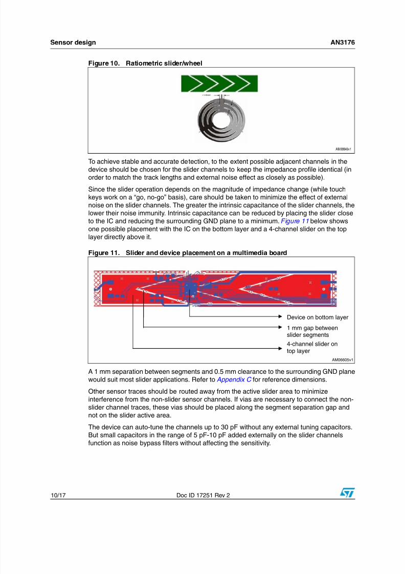
To achieve stable and accurate detection, to the extent possible adjacent channels in thedevice should be chosen for the slider channels to keep the impedance profile identical (inorder to match the track lengths and external noise effect as closely as possible).
Since the slider operation depends on the magnitude of impedance change (while touch
keys work on a “go, no-go” basis), care should be taken to minimize the effect of externalnoise on the slider channels. The greater the intrinsic capacitance of the slider channels, thelower their noise immunity. Intrinsic capacitance can be reduced by placing the slider closeto the IC and reducing the surrounding GND plane to a minimum. Figure 11 below showsone possible placement with the IC on the bottom layer and a 4-channel slider on the toplayer directly above it.
Figure 11. Slider and device placement on a multimedia board
A 1 mm separation between segments and 0.5 mm clearance to the surrounding GND planewould suit most slider applications. Refer to Appendix C for reference dimensions.
Other sensor traces should be routed away from the active slider area to minimizeinterference from the non-slider sensor channels. If vias are necessary to connect the non-slider channel traces, these vias should be placed along the segment separation gap andnot on the slider active area.
The device can auto-tune the channels up to 30 pF without any external tuning capacitors.But small capacitors in the range of 5 pF-10 pF added externally on the slider channelsfunction as noise bypass filters without affecting the sensitivity.

8/2/2019 CD 00267919
http://slidepdf.com/reader/full/cd-00267919 11/17
AN3176 Reference schematic diagram
Doc ID 17251 Rev 2 11/17
Appendix A Reference schematic diagram
Figure 12. Reference schematic diagram
AM06651v1
S 0
1
S 1
2
S 2
3
G N D
4
V I O
5
S 1 6
6
S 1 7
7
S 3
8
S 4
9
S 5
1 0
S 61 1
S 71 2
G N D1 3
V I O1 4
S 1 81 5
S 1 91 6
V C C1 7
I N T1 8
A D D R 01 9
S C L2 0
S D A
2 1
R S T
2 2
A D D R 1
2 3
C R E F
2 4
S 2 0
2 5
S 2 1
2 6
G N D
2 7
S 8
2 8
S 9
2 9
V I O
3 0
S 1 0 3 1
S 1 1 3 2
S 1 2 3 3
S 1 3 3 4
V I O 3 5
G N D 3 6
S 2 2 3 7
S 2 3 3 8
S 1 4 3 9
S 1 5 4 0
U 1
S T M P E 2 4 M 3
1
D 1
D 2
D 3
D 4
D 5
D 6
D 7
D 8
D 9
D 1 0
2 2 0
R 1
2 2 0
R 2
2 2 0
R 3
2
2 0
R 4
2 2 0
R 5
2 2 0
R 6
2 2 0
R 7
2 2 0
R 8
2 2 0
R 9
2 2 0
R 1 0
5 V
1 0 p F
C 1
1 0 p F
C 2
1 0 p F
C 3
1 0 p F
C 4
1 0 p F
C 5
1 0 p F
C 6
1 0 p F
C 7
1 0 p F
C 8
1 0 p F
C 9
1 0 p F
C 1 0
1 0 p F
C 1 1
1 0 p F
C 1 2
1 0 p F
C R E F
S L 0
S L 1
S L 2
S L 3
S L 0
S L 1
S L 2
S L 3
D S L 0
D S L
3
B 2
D B 2
B 3
D B 3
B 5
D B 5
B 6 D B 6
B 4
D B 4
B 7
D B 7
B 8
D B 8
D S L 3
D B 1
D B 2
D B 3
D B 4
D B 5
D B 6
D B 7
D B 8
B 1
B 2
B 3
B 4
B 5
B 6
B 7
B 8
C R E F
C R E F
G N D
G N D
G N D
G N D
S C L
S D A
1 0 K
R S T
1 0 K
R S C L
1 0 K
R S D A
3 V 3
4 . 7 u F
C 1 3
G N D
G N D
1 0 K
R I N T
I N T
1
2
3
4
5
6
7
8
9
1 0
C O N
S C L
S D A
G N D
I N T
G N D
B 1
D B 1
D S L 0
1 0 0 n F
C 1 9
3 V 3
R S T
R S T
3 V 3
3 V 3
3 V 3
3 V 3
4 . 7 u F
C 1 4
1 0 0 n F
C 1 5
3 V 3
1 0 0 n F
C 1 7
G N D
1 0 0 n F
C 1 6
1 0 0 n F
C 1 8
G N D

8/2/2019 CD 00267919
http://slidepdf.com/reader/full/cd-00267919 12/17
Reference PCB layout of 4-layer multimedia board AN3176
12/17 Doc ID 17251 Rev 2
Appendix B Reference PCB layout of 4-layer multimediaboard
Figure 13. Multimedia board for a notebook application
Figure 14. PCB layout of multimedia board - top layer (sensor pads with GND mesh)
Figure 15. PCB layout of multimedia board - mid layer 1 (no routing except for oneshort 3.3 V trace)
Figure 16. PCB layout of multimedia board - mid layer 2 (with all the sensor tracesand a small mesh GND plane)
4-channel ratiometric slider 10 mm x 10 mm touchkeys with LEDs in the center

8/2/2019 CD 00267919
http://slidepdf.com/reader/full/cd-00267919 13/17
AN3176 Reference PCB layout of 4-layer multimedia board
Doc ID 17251 Rev 2 13/17
Figure 17. PCB layout of multimedia board - bottom layer (all I2C traces, PWM tracesand non-sensor routing with a GND mesh)
8/2/2019 CD 00267919
http://slidepdf.com/reader/full/cd-00267919 14/17
Reference dimensions for slider and touchkey for multimedia board AN3176
14/17 Doc ID 17251 Rev 2
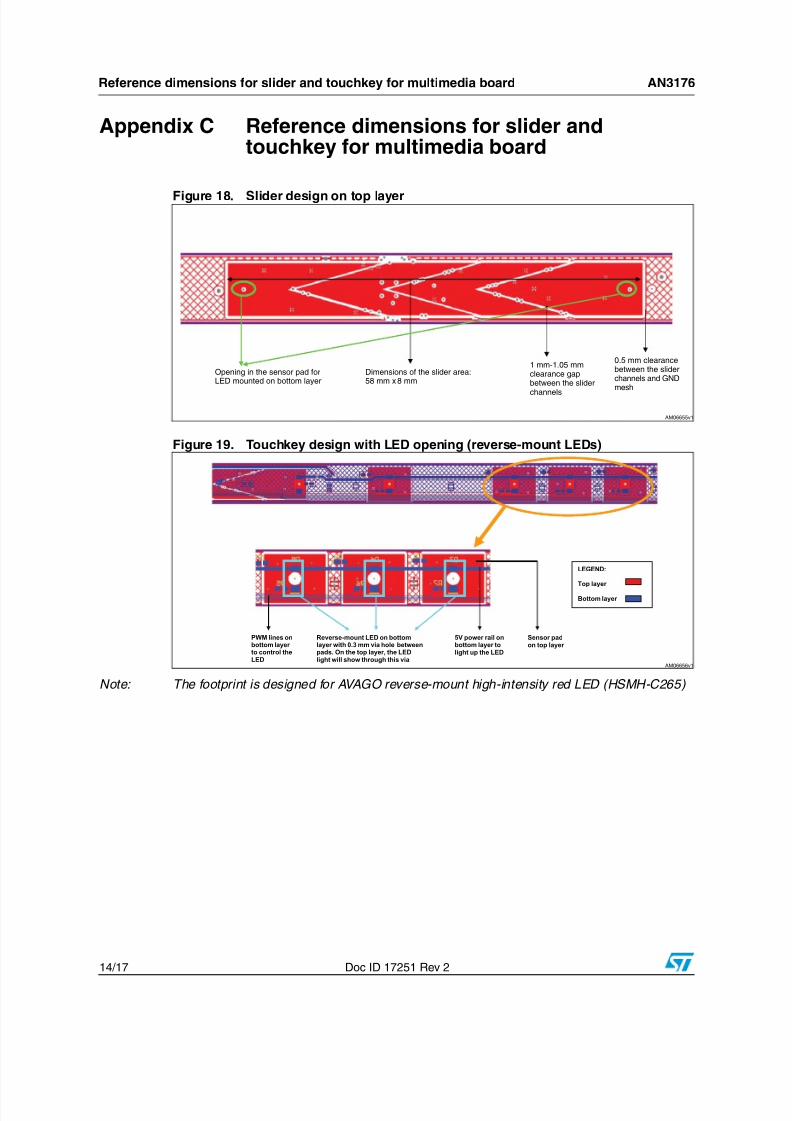
Appendix C Reference dimensions for slider andtouchkey for multimedia board
Figure 18. Slider design on top layer
Figure 19. Touchkey design with LED opening (reverse-mount LEDs)
Note: The footprint is designed for AVAGO reverse-mount high-intensity red LED (HSMH-C265)
Reverse-mount LED on bottomlayer with 0.3 mm via hole betweenpads. On the top layer, the LEDlight will show through this via
5V power rail onbottom layer tolight up the LED
PWM lines onbottom layer to control theLED
Sensor padon top layer
LEGEND:
Top layer
Bottom layer
8/2/2019 CD 00267919
http://slidepdf.com/reader/full/cd-00267919 15/17
AN3176 Bill of material
Doc ID 17251 Rev 2 15/17
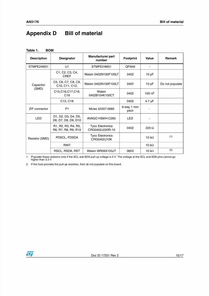
Appendix D Bill of material
Table 1. BOM
Description DesignatorManufacturer part
numberFootprint Value Remark
STMPE24M31 U1 STMPE24M31 QFN40 -
Capacitor
(SMD)
C1, C2, C3, C4,
CREFWalsin 0402N100F100LT 0402 10 pF
C5, C6, C7, C8, C9,
C10, C11, C12,Walsin 0402N100F100LT 0402 10 pF Do not populate
C15,C16,C17,C18,
C19
Walsin
0402B104K100CT0402 100 nF
C13, C18 0402 4.7 µF
ZIF connector P1 Molex 52207-06856-way 1 mm
pitch-
LEDD1, D2, D3, D4, D5,
D6, D7, D8, D9, D10AVAGO HSMH-C265 LED -
Resistor (SMD)
R1, R2, R3, R4, R5,
R6, R7, R8, R9, R10
Tyco Electronics
CRG0402J220R-100402 220 Ω
PDSCL, PDSDATyco Electronics
CRG0402J10K10 kΩ (1)
RINT 10 kΩ
RSCL, RSDA, RST Walsin WR06X103JT 0603 10 kΩ
(2)
1. Populate these resistors only if the SCL and SDA pull-up voltage is 5 V. The voltage at the SCL and SDA pins cannot gohigher than 3.3 V
2. If the host provides the pull-up resistors, then do not populate on this board

8/2/2019 CD 00267919
http://slidepdf.com/reader/full/cd-00267919 16/17
Revision history AN3176
16/17 Doc ID 17251 Rev 2
Revision history
Table 2. Document revision history
Date Revision Changes
10-Jun-2010 1 Initial release.
19-Apr-2011 2 Updated S-Touch ® .

8/2/2019 CD 00267919
http://slidepdf.com/reader/full/cd-00267919 17/17
AN3176
Doc ID 17251 Rev 2 17/17
Please Read Carefully:
Information in this document is provided solely in connection with ST products. STMicroelectronics NV and its subsidiaries (“ST”) reserve the
right to make changes, corrections, modifications or improvements, to this document, and the products and services described herein at any
time, without notice.
All ST products are sold pursuant to ST’s terms and conditions of sale.
Purchasers are solely responsible for the choice, selection and use of the ST products and services described herein, and ST assumes no
liability whatsoever relating to the choice, selection or use of the ST products and services described herein.
No license, express or implied, by estoppel or otherwise, to any intellectual property rights is granted under this document. If any part of this
document refers to any third party products or services it shall not be deemed a license grant by ST for the use of such third party products
or services, or any intellectual property contained therein or considered as a warranty covering the use in any manner whatsoever of such
third party products or services or any intellectual property contained therein.
UNLESS OTHERWISE SET FORTH IN ST’S TERMS AND CONDITIONS OF SALE ST DISCLAIMS ANY EXPRESS OR IMPLIED
WARRANTY WITH RESPECT TO THE USE AND/OR SALE OF ST PRODUCTS INCLUDING WITHOUT LIMITATION IMPLIED
WARRANTIES OF MERCHANTABILITY, FITNESS FOR A PARTICULAR PURPOSE (AND THEIR EQUIVALENTS UNDER THE LAWS
OF ANY JURISDICTION), OR INFRINGEMENT OF ANY PATENT, COPYRIGHT OR OTHER INTELLECTUAL PROPERTY RIGHT.
UNLESS EXPRESSLY APPROVED IN WRITING BY AN AUTHORIZED ST REPRESENTATIVE, ST PRODUCTS ARE NOT
RECOMMENDED, AUTHORIZED OR WARRANTED FOR USE IN MILITARY, AIR CRAFT, SPACE, LIFE SAVING, OR LIFE SUSTAINING
APPLICATIONS, NOR IN PRODUCTS OR SYSTEMS WHERE FAILURE OR MALFUNCTION MAY RESULT IN PERSONAL INJURY,
DEATH, OR SEVERE PROPERTY OR ENVIRONMENTAL DAMAGE. ST PRODUCTS WHICH ARE NOT SPECIFIED AS "AUTOMOTIVE
GRADE" MAY ONLY BE USED IN AUTOMOTIVE APPLICATIONS AT USER’S OWN RISK.
Resale of ST products with provisions different from the statements and/or technical features set forth in this document shall immediately void
any warranty granted by ST for the ST product or service described herein and shall not create or extend in any manner whatsoever, any
liability of ST.
ST and the ST logo are trademarks or registered trademarks of ST in various countries.
Information in this document supersedes and replaces all information previously supplied.
The ST logo is a registered trademark of STMicroelectronics. All other names are the property of their respective owners.
© 2011 STMicroelectronics - All rights reserved
STMicroelectronics group of companies
Australia - Belgium - Brazil - Canada - China - Czech Republic - Finland - France - Germany - Hong Kong - India - Israel - Italy - Japan -
Malaysia - Malta - Morocco - Philippines - Singapore - Spain - Sweden - Switzerland - United Kingdom - United States of America
www.st.com