Embed Size (px)
Citation preview

CC256xCQFN-EM
User's Guide
Literature Number: SWRU493ANovember 2016–Revised November 2016

2 SWRU493A–November 2016–Revised November 2016Submit Documentation Feedback
Copyright © 2016, Texas Instruments Incorporated
Table of Contents
Contents
1 Introduction to the CC256xCQFN-EM Board ............................................................................ 41.1 Key Features.............................................................................................................. 51.2 QFN EM Board Applications............................................................................................ 5
2 Module Description .............................................................................................................. 63 Module Detailed Description.................................................................................................. 7
3.1 Pin Description ........................................................................................................... 73.1.1 Board Jumpers................................................................................................ 7
3.1.1.1 Measuring Current Consumption ...................................................................... 73.1.2 Antenna and U.FL Selector ................................................................................. 73.1.3 RF Connectors................................................................................................ 83.1.4 Debug Header ................................................................................................ 93.1.5 COM Connector ............................................................................................. 10
3.2 Clock Inputs ............................................................................................................. 124 Module Dimensions ............................................................................................................ 125 Tools and Software............................................................................................................. 13
5.1 TI's Bluetooth® Software Solution..................................................................................... 135.2 Evaluation Platforms ................................................................................................... 135.3 Bluetooth® Hardware Evaluation Tool................................................................................ 13
6 Certification ....................................................................................................................... 147 Life Support Policy ............................................................................................................. 148 Related Documents ............................................................................................................ 14Revision History.......................................................................................................................... 15

www.ti.com
3SWRU493A–November 2016–Revised November 2016Submit Documentation Feedback
Copyright © 2016, Texas Instruments Incorporated
List of Figures
List of Figures1 CC256xCQFN-EM Board ................................................................................................... 42 CC2564xCQFN-EM Highlights............................................................................................. 63 CC256xCQFN-EM Block Diagram......................................................................................... 74 CC256XCQFN-EM PCM Role Selection for RF Connectors .......................................................... 95 COM Connector Pinout.................................................................................................... 106 CC256XCQFN-EM Hardware Modifications for COM Connector.................................................... 117 CC256xC Clocking Scheme .............................................................................................. 128 CC256xCQFN-EM Hardware Configuration ........................................................................... 13
List of Tables1 Jumper Configuration ....................................................................................................... 72 RF1 ............................................................................................................................ 83 RF2 ............................................................................................................................ 84 DEBUG HDR ................................................................................................................ 95 COM CARD ................................................................................................................. 106 Module Dimensions ........................................................................................................ 12

Copyright © 2016, Texas Instruments Incorporated
4 SWRU493A–November 2016–Revised November 2016Submit Documentation Feedback
Copyright © 2016, Texas Instruments Incorporated
CC256xCQFN-EM
Code Composer Studio is a trademark of Texas Instruments.Bluetooth is a registered trademark of Bluetooth SIG, Inc.All other trademarks are the property of their respective owners.
User's GuideSWRU493A–November 2016–Revised November 2016
CC256xCQFN-EM
1 Introduction to the CC256xCQFN-EM BoardThis user's guide is intended for use with TI's Bluetooth® development platform, the CC256xCQFN-EMboard (see Figure 1). This guide helps users quickly get started integrating the board with TI's evaluationplatforms and software SDKs. In addition, this user's guide describes the components and configurationsof the board so that users can quickly get started using it for various Bluetooth applications.
This guide provides information about the module so that developers can use the board specifics to applyit to their applications. Module information and capabilities, including pin descriptions as well as availablesoftware and tools, enhance the user's out-of-box experience.
Figure 1. CC256xCQFN-EM Board

www.ti.com Introduction to the CC256xCQFN-EM Board
5SWRU493A–November 2016–Revised November 2016Submit Documentation Feedback
Copyright © 2016, Texas Instruments Incorporated
CC256xCQFN-EM
1.1 Key Features• Bluetooth specification 4.1 / 4.2• Fast time to market• Easy PCB layout using cadence tools• 4-layer PCB design• Bluetooth and Bluetooth low energy• TI's Bluetooth royalty-free stack with profiles• FCC, IC, and Bluetooth SIG compliant• High sensitivity (–93 dBm typical)• Shield enabled for immunity• H4 UART and PCM/I2S interface
1.2 QFN EM Board ApplicationsThe following are example embedded wireless applications:• Wireless Audio Solutions• mPOS• Medical Devices• Set-Top Boxes (STBs)• Wearable Devices• Sensor Hub, Sensor Gateway
– Home and Factory Automation

U.FL Connector
QFN Reference Design
Debug Header Pin 1
COM Connector
VDD_IO Jumper 1
PCB Copper
Antenna
17
18
15
16
13
14 12
11
10
9
8
7
6
5
4
3 1
VBAT Jumper 2
Text
Module Description www.ti.com
6 SWRU493A–November 2016–Revised November 2016Submit Documentation Feedback
Copyright © 2016, Texas Instruments Incorporated
CC256xCQFN-EM
2 Module DescriptionThe CC256xC QFN EM board is the development environment for the CC256x family and plugs into TI'sMSP432™ LaunchPad™ through the BOOST-CCEMADAPTER board.
This family is based on TI's CC256xC integrated circuit and uses a host controller interface (HCI), a cost-effective and flexible means for implementing a Bluetooth network. The HCI reduces BOM cost byeliminating redundant processing capacity and gives designers the flexibility to work with a controller oftheir choice, because the Bluetooth stack resides and executes on the host processor of the application.Figure 2 highlights various aspects of the CC256xCQFN-EM board.
Figure 2. CC2564xCQFN-EM Highlights
The CC256xCQFN-EM board is intended for evaluation purposes and works with TI's HardwareDevelopment Kit. See Section 6 for more information.
To help implement this reference design, schematics and layout files are available on the CC256x MainWiki page.

CC256xCQFN-EM Board
Copyright © 2016, Texas Instruments Incorporated
Setup Jumper
CC256xCReference Design
(Inside Shield)
RFConnector
COMConnector
VDD 3.3 V
PCM / I2S
H4 UART
SLOW CLOCK
nSHUTD
www.ti.com Module Detailed Description
7SWRU493A–November 2016–Revised November 2016Submit Documentation Feedback
Copyright © 2016, Texas Instruments Incorporated
CC256xCQFN-EM
3 Module Detailed DescriptionThe reference files including schematics, layout, and BOM for the CC256xCQFN-EM board can be foundat: CC256xCQFN-EM Reference Design.
Figure 3 shows a block diagram depicting the I/Os of the QFN board that are required for interfacing to thehost controller. These I/Os can be interfaced to the host controller through either the COM connector orthe RF1 and RF2 sockets.
Figure 3. CC256xCQFN-EM Block Diagram
3.1 Pin Description
3.1.1 Board JumpersFor correct operation, ensure both jumpers are placed for connecting power to the device as follows inTable 1.
Table 1. Jumper Configuration
Jumper DescriptionVBAT_CC Main power supply for CC256xCVDD_1V8 Supplies power to CC256xC I/Os
3.1.1.1 Measuring Current ConsumptionThese jumpers can also be used to measure the current consumption by placing current sense resistorson R10 for VBAT_CC and on R7 for VDD_1V8. Both these resistors are 0.10 Ω, 1/4 W. The VBAT_CCjumper can be used to to measure the voltage and power consumed by the CC256xC, including RF TXand RX while the VDD_IO jumper can be used to measure voltage and power consumed by the digitalI/Os.
3.1.2 Antenna and U.FL SelectorThe board can be configured to route the RF output from the CC256xC to the onboard copper antenna orthe onboard U.FL connector. This configuration is done by placing the resistor in either the R29 or R30position which has negligible resistance of 0 Ω. R30 connects the RF to the U.FL while R29 connects tothe copper antenna. The U.FL connector is used for conducted testing of the RF. The Bluetooth HardwareEvaluation Tool (BHET) can be used to test basic RF functionality on this board.

Module Detailed Description www.ti.com
8 SWRU493A–November 2016–Revised November 2016Submit Documentation Feedback
Copyright © 2016, Texas Instruments Incorporated
CC256xCQFN-EM
3.1.3 RF ConnectorsThe RF1 and RF2 connectors can be sued to mount the TI MSP432 platform using the BOOST-CCEMADAPTER board. The RF I/Os are all at 3.3-V levels; this enables seamless integration of the hostusing TI's platforms that comes preinstalled with EM headers. Table 2 and Table 3 describe the standardpinout.
Table 2. RF1
Pin No. EM Adapter Pin Assignment Pin No. EM Adapter Pin Assignment1 GND 2 NC3 MODULE_UART_CTS 4 NC5 SLOW_CLK 6 NC7 MODULE_UART_RX 8 NC9 MODULE_UART_TX 10 NC11 NC (not connected) 12 NC13 NC 14 NC15 NC 16 NC17 NC 18 NC19 GND 20 NC
Table 3. RF2
Pin No. EM Adapter Pin Assignment Pin No. EM Adapter Pin Assignment1 NC 2 GND3 NC 4 NC5 NC 6 NC7 3.3 V 8 MODULE_AUDIO_DATA_OUT9 3.3 V 10 MODULE_AUDIO_DATA_IN11 MODULE_AUDIO_FSYNC 12 NC13 NC 14 NC15 NC 16 NC17 MODULE_AUDIO_CLK 18 MODULE_UART_RTS19 WCS_NSHUTD 20 NC
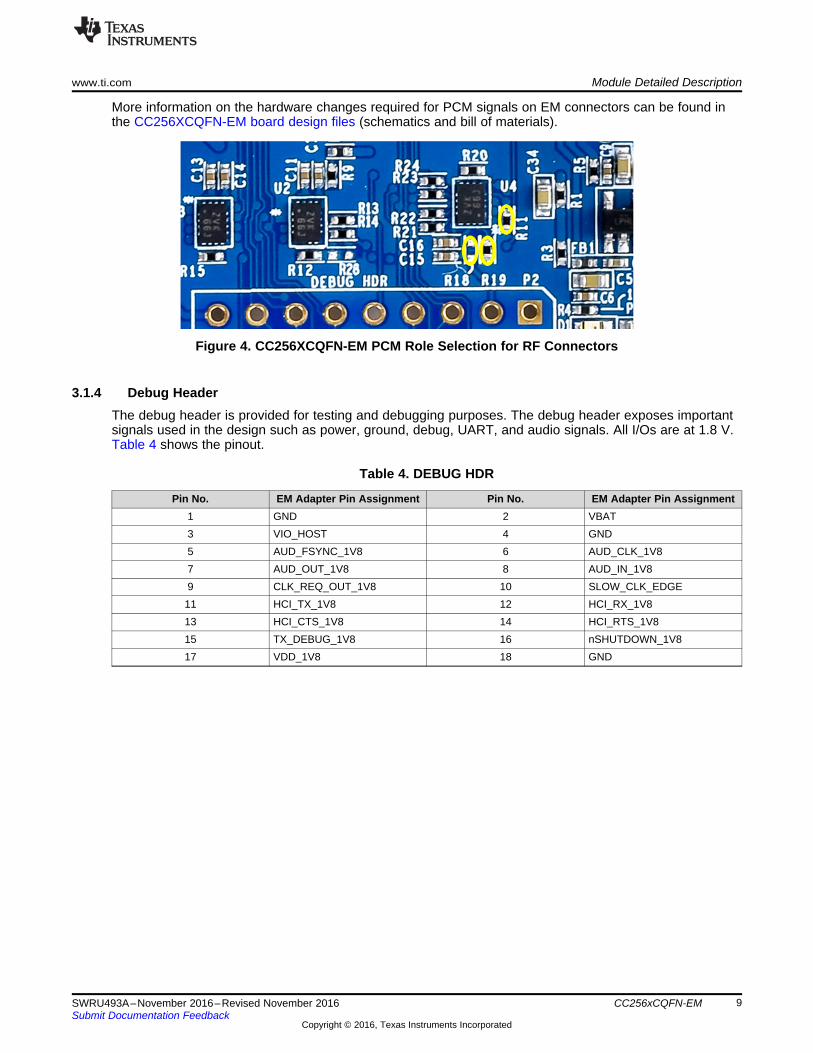
For complete evaluation of the audio applications while using the RF connectors (a.k.a. EM connectors),the level shifter U4 must be properly configured in order to ensure proper direction of PCM signals.• When using CC256XC as PCM master role (for A3DP Sink, HFP and HSP profiles),
– R19 must be populated with 10K resistor.– R18 and R11 must be unpopulated (removed).
• When using CC256XC as PCM slave (for A3DP Source profile),– R18 must be populated with 10K resistor.– R19 and R11 must be unpopulated (removed),
www.ti.com Module Detailed Description
9SWRU493A–November 2016–Revised November 2016Submit Documentation Feedback
Copyright © 2016, Texas Instruments Incorporated
CC256xCQFN-EM
More information on the hardware changes required for PCM signals on EM connectors can be found inthe CC256XCQFN-EM board design files (schematics and bill of materials).
Figure 4. CC256XCQFN-EM PCM Role Selection for RF Connectors
3.1.4 Debug HeaderThe debug header is provided for testing and debugging purposes. The debug header exposes importantsignals used in the design such as power, ground, debug, UART, and audio signals. All I/Os are at 1.8 V.Table 4 shows the pinout.
Table 4. DEBUG HDR
Pin No. EM Adapter Pin Assignment Pin No. EM Adapter Pin Assignment1 GND 2 VBAT3 VIO_HOST 4 GND5 AUD_FSYNC_1V8 6 AUD_CLK_1V87 AUD_OUT_1V8 8 AUD_IN_1V89 CLK_REQ_OUT_1V8 10 SLOW_CLK_EDGE11 HCI_TX_1V8 12 HCI_RX_1V813 HCI_CTS_1V8 14 HCI_RTS_1V815 TX_DEBUG_1V8 16 nSHUTDOWN_1V817 VDD_1V8 18 GND

Module Detailed Description www.ti.com
10 SWRU493A–November 2016–Revised November 2016Submit Documentation Feedback
Copyright © 2016, Texas Instruments Incorporated
CC256xCQFN-EM
3.1.5 COM ConnectorThe COM connector, or edge card, is used to interface with TI's MPUs such as the AM437x and AM335xEVMs. As shown in Figure 5, the COM connector provides HCI, audio, slow clock, shutdown, and debuginterfaces to the host connected through the edge card. All I/Os for the COM connector are at 1.8 V.Some components must be DNI to use the COM connector. See the BOM for details.
Figure 5. COM Connector Pinout
Table 5 lists the COM card pinout.
Table 5. COM CARD
Pin No. Relevant COM Connector Pin Assignment1 SLOW_CLK_EDGE8 1V8_IN52 AUD_CLK_1V854 AUD_FSYNC_1V856 AUD_IN_1V858 AUD_OUT_1V866 HCI_TX_1V868 HCI_RX_1V870 HCI_CTS_1V872 HCI_RTS_1V876 TX_DEBUG_1V889 nSHUTDOWN_1V8

www.ti.com Module Detailed Description
11SWRU493A–November 2016–Revised November 2016Submit Documentation Feedback
Copyright © 2016, Texas Instruments Incorporated
CC256xCQFN-EM
Pins 3, 9, 19, 37, 47, 63, 77, 83, 87, 95, and 97, as well as 2, 6, 18, 22, 42, 60, 64, and 92 are connectedto ground.
All other pins are NC.
Some components must be removed (DNI) and R2 must be populated on the CC256XCQFN-EM to usethe COM connector with the AM335x evaluation module (TMDXEVM3358) or similar Sitara EVM.• EM1, EM2, U2, U3, and U4 must be unpopulated (removed).• R2 (0 Ω) must be populated.
More information on the hardware changes required for the COM connector are in the CC256XCQFN-EMboard design files (schematics and bill of materials).
Figure 6. CC256XCQFN-EM Hardware Modifications for COM Connector

CC256xCDevice
RF Connector
Oscillator (onboard)
COM Connector
SLOW_CLK_IN
Module Detailed Description www.ti.com
12 SWRU493A–November 2016–Revised November 2016Submit Documentation Feedback
Copyright © 2016, Texas Instruments Incorporated
CC256xCQFN-EM
3.2 Clock InputsThe slow clock can come from two sources, internal and external to the board. The CC256xCQFN-EM hasthe option to place the slow clock on the board or source it from an external source. The source isconnected to the SLOW_CLK_IN (see Figure 7) and can be a digital signal in the range of 0 to 1.8 V.
The frequency accuracy of the slow clock must be 32.768 kHz and ±250 ppm for Bluetooth use (accordingto the Bluetooth specification).
When the MSP432 Launchpad is connected, the SLOW_CLK_IN signal, is sourced from the oscillator onthe CC256xCQFN-EM board, therefore no additional clock source is needed.
Figure 7. CC256xC Clocking Scheme
4 Module DimensionsTable 6 lists the module dimensions.
Table 6. Module Dimensions
No. Item Dimension (in) Tolerance Remark1 Width 1.550 ± 0.001 Smaller at COM end2 Length 2.125 ± 0.001 —3 Height 0.062 ± 0.001 —

www.ti.com Tools and Software
13SWRU493A–November 2016–Revised November 2016Submit Documentation Feedback
Copyright © 2016, Texas Instruments Incorporated
CC256xCQFN-EM
5 Tools and Software
5.1 TI's Bluetooth® Software SolutionThe Bluetooth software based solution is based on TI's Bluetooth stack, such as theCC2564CMSP432BTBLESW. Detailed documentation is in the previous SDK.
5.2 Evaluation PlatformsTI supports the MSP432 LaunchPad (MSP-EXP432P401R).
In addition, a software development environment, for example Code Composer Studio™, is required. Fora detailed description on use of these tools, refer to the CC256xC EVM Platform. Evaluation kits andmodules are available through TI's network of authorized distributors.
Figure 8 shows the CC256xCQFN-EM board mounted to the MSP-EXP432P401R using the BOOST-CCEMADAPTER board, which uses the RF1 and RF2 interface board.
Figure 8. CC256xCQFN-EM Hardware Configuration
5.3 Bluetooth® Hardware Evaluation ToolThe CC256x Bluetooth Hardware Evaluation Tool can be downloaded as a complete package from TI.This program is an intuitive, user-friendly tool to test TI's Bluetooth chips including this CC256xCQFN-EMboard. More specifically, the program is used to measure RF performance of TI's Bluetooth chips.

Certification www.ti.com
14 SWRU493A–November 2016–Revised November 2016Submit Documentation Feedback
Copyright © 2016, Texas Instruments Incorporated
CC256xCQFN-EM
6 CertificationCertifications for the CC256xCQFN-EM board include the CE Mark - Conformité Européenne. TheCC256xC is also in the process of being certified as a Bluetooth controller subsystem by Bluetooth SIG(Special Interest Group).
NOTE: This device is an engineering development board and cannot be used in an end product.
7 Life Support Policy
CAUTIONThis TI product is not designed for use in life support appliances, devices, orsystems where malfunction can reasonably be expected to result in asignificant personal injury to the user, or as a critical component in any lifesupport device or system whose failure to perform can be reasonably expectedto cause the failure of the life support device or system, or to affect its safety oreffectiveness. TI customers using or selling these products for use in suchapplications do so at their own risk and agree to fully indemnify TI for anydamages resulting.
8 Related Documents• CC2564C Data Sheet• CC256x System Design Guide• CC256xQFN PCB Guidelines• QFN Reference Design

www.ti.com Revision History
15SWRU493A–November 2016–Revised November 2016Submit Documentation Feedback
Copyright © 2016, Texas Instruments Incorporated
Revision History
Revision HistoryNOTE: Page numbers for previous revisions may differ from page numbers in the current version.
Changes from Original (November 2016) to A Revision ................................................................................................ Page
• Added text to RF Connectors section .................................................................................................. 8• Added CC256XCQFN-EM PCM Role Selection for RF Connectors ............................................................... 9• Added text in COM Connector section................................................................................................ 11• Added CC256XCQFN-EM Hardware Modifications for COM Connector image ................................................ 11

IMPORTANT NOTICE
Texas Instruments Incorporated and its subsidiaries (TI) reserve the right to make corrections, enhancements, improvements and otherchanges to its semiconductor products and services per JESD46, latest issue, and to discontinue any product or service per JESD48, latestissue. Buyers should obtain the latest relevant information before placing orders and should verify that such information is current andcomplete. All semiconductor products (also referred to herein as “components”) are sold subject to TI’s terms and conditions of salesupplied at the time of order acknowledgment.TI warrants performance of its components to the specifications applicable at the time of sale, in accordance with the warranty in TI’s termsand conditions of sale of semiconductor products. Testing and other quality control techniques are used to the extent TI deems necessaryto support this warranty. Except where mandated by applicable law, testing of all parameters of each component is not necessarilyperformed.TI assumes no liability for applications assistance or the design of Buyers’ products. Buyers are responsible for their products andapplications using TI components. To minimize the risks associated with Buyers’ products and applications, Buyers should provideadequate design and operating safeguards.TI does not warrant or represent that any license, either express or implied, is granted under any patent right, copyright, mask work right, orother intellectual property right relating to any combination, machine, or process in which TI components or services are used. Informationpublished by TI regarding third-party products or services does not constitute a license to use such products or services or a warranty orendorsement thereof. Use of such information may require a license from a third party under the patents or other intellectual property of thethird party, or a license from TI under the patents or other intellectual property of TI.Reproduction of significant portions of TI information in TI data books or data sheets is permissible only if reproduction is without alterationand is accompanied by all associated warranties, conditions, limitations, and notices. TI is not responsible or liable for such altereddocumentation. Information of third parties may be subject to additional restrictions.Resale of TI components or services with statements different from or beyond the parameters stated by TI for that component or servicevoids all express and any implied warranties for the associated TI component or service and is an unfair and deceptive business practice.TI is not responsible or liable for any such statements.Buyer acknowledges and agrees that it is solely responsible for compliance with all legal, regulatory and safety-related requirementsconcerning its products, and any use of TI components in its applications, notwithstanding any applications-related information or supportthat may be provided by TI. Buyer represents and agrees that it has all the necessary expertise to create and implement safeguards whichanticipate dangerous consequences of failures, monitor failures and their consequences, lessen the likelihood of failures that might causeharm and take appropriate remedial actions. Buyer will fully indemnify TI and its representatives against any damages arising out of the useof any TI components in safety-critical applications.In some cases, TI components may be promoted specifically to facilitate safety-related applications. With such components, TI’s goal is tohelp enable customers to design and create their own end-product solutions that meet applicable functional safety standards andrequirements. Nonetheless, such components are subject to these terms.No TI components are authorized for use in FDA Class III (or similar life-critical medical equipment) unless authorized officers of the partieshave executed a special agreement specifically governing such use.Only those TI components which TI has specifically designated as military grade or “enhanced plastic” are designed and intended for use inmilitary/aerospace applications or environments. Buyer acknowledges and agrees that any military or aerospace use of TI componentswhich have not been so designated is solely at the Buyer's risk, and that Buyer is solely responsible for compliance with all legal andregulatory requirements in connection with such use.TI has specifically designated certain components as meeting ISO/TS16949 requirements, mainly for automotive use. In any case of use ofnon-designated products, TI will not be responsible for any failure to meet ISO/TS16949.
Products ApplicationsAudio www.ti.com/audio Automotive and Transportation www.ti.com/automotiveAmplifiers amplifier.ti.com Communications and Telecom www.ti.com/communicationsData Converters dataconverter.ti.com Computers and Peripherals www.ti.com/computersDLP® Products www.dlp.com Consumer Electronics www.ti.com/consumer-appsDSP dsp.ti.com Energy and Lighting www.ti.com/energyClocks and Timers www.ti.com/clocks Industrial www.ti.com/industrialInterface interface.ti.com Medical www.ti.com/medicalLogic logic.ti.com Security www.ti.com/securityPower Mgmt power.ti.com Space, Avionics and Defense www.ti.com/space-avionics-defenseMicrocontrollers microcontroller.ti.com Video and Imaging www.ti.com/videoRFID www.ti-rfid.comOMAP Applications Processors www.ti.com/omap TI E2E Community e2e.ti.comWireless Connectivity www.ti.com/wirelessconnectivity
Mailing Address: Texas Instruments, Post Office Box 655303, Dallas, Texas 75265Copyright © 2016, Texas Instruments Incorporated