Embed Size (px)
Citation preview
Case study of a Rapid Control Prototypingsystem based on Xilinx System Generator
Fallstudie av ett Rapid Control Prototyping-system baserat på Xilinx System Generator
MARIA BORGSTRÖM
Master’s Thesis at KTH/ICT and ABB AB
Supervisors:Johnny Öberg - KTH/ICT
Héctor Zelaya de la Parra - ABB AB, Roger Mellander - ABB ABExaminer:
Ingo Sander - KTH/ICT
KTH/TRITA/ICT/EX-2010:30


AbstractTime, money and quality are three important parameters for compet-itive industry companies and Rapid Control Prototyping is a conceptthat is used for improving the design process of for example a mecha-tronic system. It implies working with models in a high level programthat automatically generates low level code. This saves time consumingcode writing and by working with models a part in an algorithm caneasily be changed or replaced without affecting other parts.
The Rapid Control Prototyping tool Xilinx System Generator thatruns from Simulink is here investigated. Implementation of the FieldOriented Control algorithm for controlling a motor serves as main sub-ject for the investigation. A library with ready-to-use blocks is createdfor having the possibility to implement other control algorithms in thefuture in a fast, graphical, intuitive and user friendly way.
It is shown the advantage of using an FPGA with its parallelismand re-programmable characteristics when implementing a motor con-trol algorithm. It provides a high bandwidth and therefore a possibilityto control several motors with one FPGA. By programming the FPGAwith a Rapid Control Prototyping tool like Xilinx System Generator theopportunity to in an easy way change different parts becomes obvious.To use Model Based Design and Rapid Control Prototyping conceptsextensive code writing is avoided and by that for example syntax errors.The gap between the software engineer and the hardware engineer re-duces and the possibility to work in both of the domains is given.
Keywords: Rapid Control Prototyping, Xilinx System Generator, FieldOriented Control

SammanfattningFallstudie av ett Rapid Control Prototyping-system
baserat på Xilinx System Generator
Tid, pengar och kvalitet är tre viktiga parametrar för vinstinriktadeföretag och Rapid Control Prototyping är ett koncept som användsför att förbättra designprocessen av till exempel ett mekatroniksystem.Rapid Control Prototyping innebär att jobba med modeller i ett hög-nivåspråk som automatiskt genererar lågnivåkod. Detta besparar tid-skrävande kodskrivning och genom att arbeta med modeller kan en deli en algoritm lätt ändras eller bytas ut utan att påverka andra delar.
Xilinx System Generator, som körs ifrån Simulink, utvärderas häroch Rapid Control Prototyping används som ett verktyg för att im-plementera fältorienterad motorkontroll. Ett bibliotek med block klaraatt använda skapas för att ha möjligheten att implementera andra kon-trollalgoritmer i framtiden på ett snabbt, grafiskt, intuitivt och använ-darvänligt sätt.
Fördelen med att använda en FPGA, med dess parallellism ochåterprogrammerbarhet, påvisas genom implementering av en motorkon-trollalgoritm. Den ger en hög bandbredd och därigenom möjlighetenatt kontrollera flera motorer med en FPGA. Genom att programmeraFPGA:n med Rapid Control Prototyping-verktyg som Xilinx SystemGenerator blir möjligheten att på ett lätt sätt byta olika delar up-penbar. Genom att använda modellbaserad design och Rapid ControlPrototyping-konceptet undviks omfattande kodskrivning och genom detsyntaxfel. Gapet mellan mjukvaru- och hårdvaruingenjörer minskas ochmöjligheten att arbeta i de båda domänerna ges.
Nyckelord: Rapid Control Prototyping, Xilinx System Generator, Fäl-torienterad kontroll

Acknowledgments
This thesis work was performed at the Department of Automation Technologies(AT) at ABB Corporate Research (CRC) in Västerås from September 2009 to Jan-uary 2010.
I would like to thank my supervisors Héctor Zelaya de la Parra and RogerMellander at ABB with their winner spirit and their great support and encour-agement. Thanks to Héctor my dream of doing my master thesis at ABB came trueand during the way Roger was always there giving me a hand, stealing or giving mea pen when I needed it.
A special thank goes to my family Eva, Olle and Markus Borgström and OscarLucas Villalón for all their love and faith in me and their never-ending encour-agement and patience. I love all of you ♥
I would also like to thank Maria Nilsson for always being there as a friend andfor lending me her precious red car JAN - without "Janne" it would have beenimpossible to go to work every day.
A big hug and tusen tack to all of my friends on CRC for being there and forgiving the just mentioned precious little red car a push when it was needed duringthe coldest winter days.
It has been a pleasure!
Maria BorgströmJanuary 2009

Contents
1 Introduction 11.1 Purpose . . . . . . . . . . . . . . . . . . . . . . . . . . . . . . . . . . 11.2 Scope . . . . . . . . . . . . . . . . . . . . . . . . . . . . . . . . . . . 11.3 Definitions . . . . . . . . . . . . . . . . . . . . . . . . . . . . . . . . . 21.4 Structure . . . . . . . . . . . . . . . . . . . . . . . . . . . . . . . . . 2
2 Problem Description 52.1 Background . . . . . . . . . . . . . . . . . . . . . . . . . . . . . . . . 52.2 Problem definition . . . . . . . . . . . . . . . . . . . . . . . . . . . . 5
2.2.1 Problem statement . . . . . . . . . . . . . . . . . . . . . . . . 62.3 Related work . . . . . . . . . . . . . . . . . . . . . . . . . . . . . . . 62.4 Previous work . . . . . . . . . . . . . . . . . . . . . . . . . . . . . . . 6
3 Conceptual Background 73.1 Field Programmable Gate Array . . . . . . . . . . . . . . . . . . . . 73.2 Model Based Design . . . . . . . . . . . . . . . . . . . . . . . . . . . 83.3 Rapid Control Prototyping . . . . . . . . . . . . . . . . . . . . . . . 83.4 Hardware in the loop . . . . . . . . . . . . . . . . . . . . . . . . . . . 10
4 Theoretical Background 114.1 Field Oriented Control . . . . . . . . . . . . . . . . . . . . . . . . . . 114.2 Coordinate transformations . . . . . . . . . . . . . . . . . . . . . . . 11
4.2.1 The Clarke Transformation . . . . . . . . . . . . . . . . . . . 134.2.2 The Inverse Clarke Transformation . . . . . . . . . . . . . . . 134.2.3 The Park Transformation . . . . . . . . . . . . . . . . . . . . 144.2.4 The Inverse Park Transformation . . . . . . . . . . . . . . . . 14
4.3 Pulse Width Modulation . . . . . . . . . . . . . . . . . . . . . . . . . 164.3.1 Space Vector Pulse Width Modulation . . . . . . . . . . . . . 16
5 Development Environment 215.1 Software . . . . . . . . . . . . . . . . . . . . . . . . . . . . . . . . . . 21
5.1.1 Simulink® . . . . . . . . . . . . . . . . . . . . . . . . . . . . . 215.1.2 Xilinx System Generator . . . . . . . . . . . . . . . . . . . . . 21
5.2 Hardware . . . . . . . . . . . . . . . . . . . . . . . . . . . . . . . . . 25

5.2.1 Xilinx ML507 Evaluation Platform . . . . . . . . . . . . . . . 255.2.2 Power Board . . . . . . . . . . . . . . . . . . . . . . . . . . . 265.2.3 Brushless DC Motor . . . . . . . . . . . . . . . . . . . . . . . 265.2.4 Encoder . . . . . . . . . . . . . . . . . . . . . . . . . . . . . . 265.2.5 Experimental Setup . . . . . . . . . . . . . . . . . . . . . . . 27
6 Solution 296.1 Implementation of the different parts of the FOC algorithm in Xilinx
System Generator . . . . . . . . . . . . . . . . . . . . . . . . . . . . 296.1.1 Implementation of the coordinate transformations . . . . . . 296.1.2 Implementation of the PI regulators . . . . . . . . . . . . . . 346.1.3 Implementation of SPI ADC . . . . . . . . . . . . . . . . . . 346.1.4 Implementation of Encoder . . . . . . . . . . . . . . . . . . . 376.1.5 Implementation of Feed forward control . . . . . . . . . . . . 386.1.6 Implementation of the FOC algorithm . . . . . . . . . . . . . 406.1.7 Xilinx blocks vs. MCode . . . . . . . . . . . . . . . . . . . . . 40
7 Results 437.1 FOC algorithm . . . . . . . . . . . . . . . . . . . . . . . . . . . . . . 437.2 Normal blocks vs. the MCode Block . . . . . . . . . . . . . . . . . . 447.3 Creating a library . . . . . . . . . . . . . . . . . . . . . . . . . . . . 44
8 Discussion 478.1 HDL and RCP . . . . . . . . . . . . . . . . . . . . . . . . . . . . . . 478.2 Xilinx System Generator and LabVIEW . . . . . . . . . . . . . . . . 478.3 Lots of parameters . . . . . . . . . . . . . . . . . . . . . . . . . . . . 478.4 Different time domains . . . . . . . . . . . . . . . . . . . . . . . . . . 48
9 Conclusions 499.1 Runs from Simulink . . . . . . . . . . . . . . . . . . . . . . . . . . . 499.2 Easy implementation . . . . . . . . . . . . . . . . . . . . . . . . . . . 499.3 Parallelism . . . . . . . . . . . . . . . . . . . . . . . . . . . . . . . . 49
10 Future work 51

Bibliography 53
List of Figures
3.1 An FPGA. . . . . . . . . . . . . . . . . . . . . . . . . . . . . . . . . . . 73.2 The model based design concept. . . . . . . . . . . . . . . . . . . . . . . 83.3 To the left a counter written in VHDL code and to the right a block
with its corresponding dialog window. . . . . . . . . . . . . . . . . . . . 93.4 Hardware in the loop. . . . . . . . . . . . . . . . . . . . . . . . . . . . . 10
4.1 Field Oriented Control block diagram. FFC - Feed Forward Control,SVPWM - Space Vector Pulse Width Modulation, E - Encoder. . . . . . 12
4.2 The different coordinate systems. . . . . . . . . . . . . . . . . . . . . . . 124.3 The Clarke Transformation. . . . . . . . . . . . . . . . . . . . . . . . . . 134.4 Inverse Clarke Transformation. . . . . . . . . . . . . . . . . . . . . . . . 144.5 The Park Transformation. . . . . . . . . . . . . . . . . . . . . . . . . . . 144.6 The Inverse Park Transformation. . . . . . . . . . . . . . . . . . . . . . 154.7 Sinusoid Pulse Width Modulation. . . . . . . . . . . . . . . . . . . . . . 164.8 Simplified three phase inverter. . . . . . . . . . . . . . . . . . . . . . . . 164.9 Switching states for the three phase inverter. . . . . . . . . . . . . . . . 174.10 The reference voltage vector placed in sector one. . . . . . . . . . . . . . 184.11 The generated PWM waveform for sector one. . . . . . . . . . . . . . . . 19
5.1 Xilinx System Generator overview. . . . . . . . . . . . . . . . . . . . . . 225.2 The Black Box block. . . . . . . . . . . . . . . . . . . . . . . . . . . . . 225.3 The MCode block with its dialog window. . . . . . . . . . . . . . . . . . 235.4 Summary of implementation approaches. . . . . . . . . . . . . . . . . . . 245.5 Xilinx ML507 Evaluation Platform. . . . . . . . . . . . . . . . . . . . . . 255.6 Single drive inverter board. . . . . . . . . . . . . . . . . . . . . . . . . . 265.7 BLDC motor 57BLS01. . . . . . . . . . . . . . . . . . . . . . . . . . . . 265.8 The flat cable connections of the encoder. . . . . . . . . . . . . . . . . . 275.9 The hardware setup in the project. . . . . . . . . . . . . . . . . . . . . . 28
6.1 How the different parts were implemented. . . . . . . . . . . . . . . . . . 306.2 The Park Transform with Simulink blocks. . . . . . . . . . . . . . . . . 316.3 The Park transform with Xilinx blocks. . . . . . . . . . . . . . . . . . . 316.4 Test Bench for the Park transformation. . . . . . . . . . . . . . . . . . . 32

6.5 Output from the Park test bench. Upper plot - Simulink (continuous),middle plot - Xilinx (Fixed point 16_13), lower plot - quantization error. 33
6.6 PI current controllers for the d and q currents. . . . . . . . . . . . . . . 346.7 The SPI ADC created as a black box and the corresponding co-simulation
block. . . . . . . . . . . . . . . . . . . . . . . . . . . . . . . . . . . . . . 356.8 The output from the SPI shown on the oscilloscope during co-simulation.
Top graph - Chip select, middle graph - SPI clock, bottom graph - SPI out. 366.9 Schematic figure of the ADCs. . . . . . . . . . . . . . . . . . . . . . . . 366.10 The lower block is the Black Box for the encoder. . . . . . . . . . . . . . 376.11 Feed forward control implemented as a MCode Block. . . . . . . . . . . 386.12 m-code for implementation of feed forward in a MCode Block. . . . . . 396.13 Feed forward control implemented with blocks. . . . . . . . . . . . . . . 396.14 Implementation of the Field Oriented Control with Xilinx blocks. . . . . 406.15 Test bench for area estimation of the Clarke transformation. . . . . . . . 416.16 Test bench for area estimation of the Clarke transformation implemented
with the MCode Block. . . . . . . . . . . . . . . . . . . . . . . . . . . . 41
7.1 Result after synthesizing the FOC algorithm. . . . . . . . . . . . . . . . 437.2 Demonstration of clock cycles. . . . . . . . . . . . . . . . . . . . . . . . 447.3 Area estimation result for Clarke transformation implemented by blocks
to the left and with a MCode Block to the right. . . . . . . . . . . . . . 457.4 The different blocks created for the library. . . . . . . . . . . . . . . . . 45


Chapter 1
Introduction
Rapid Control Prototyping is something that the industry nowadays uses for im-proving their benefit. By using a high level graphical programming tool the devel-opment process goes much easier and faster than with conventional low level codeprogramming. The graphical high level program contributes by facilitating the de-velopment process, the testing and increases the possibilities to change some partsin the system in an easy way.
1.1 PurposeThe purpose is to investigate the possibility of using the high level program XilinxSystem Generator as a Rapid Control Prototyping tool. The advantage with im-plementing motor control using an FPGA will be shown since its parallelism offersimplementation of several motor axes. The fact that it is possible to work in dif-ferent regions, the FPGA domain and the motor control domain, without extensiveknowledge of hardware programming is also a showed advantage.
1.2 ScopeA motor control algorithm is implemented using Xilinx System Generator for ex-amination of its features and performance. The possibilities and advantages byworking with an FPGA, Model Based Design and Rapid Control Prototyping isalso showed.
The evaluation described is based upon testing XSG as a Rapid Control Proto-typing tool by implementing Field Oriented Control (FOC) for a motor. The FOCalgorithm is chosen but could have been substituted with any other motor controlalgorithm.
This work is not about how to optimize for examples the regulators in themotor control algorithm. The quality of the automatically generated code is notinvestigated, the main purpose is to demonstrate the benefits of implementing themotor control algorithms in an FPGA with a high level program by using the MBD
1

CHAPTER 1. INTRODUCTION
and RCP concepts. The result of occupied area on the FPGA shows out to be goodand more than sufficient for the purpose and therefore a deeper investigation is notdone.
1.3 DefinitionsThe used abbreviations are written out the first time they are mentioned and canbe found in table 1.1.
1.4 StructureThe structure of this report is as follows:
Chapter 1 - Introduction - describes the purpose and scope for this work as well asterms, abbreviations and acronyms used.Chapter 2 - Problem Description - describes the background of this project, relatedand previous work as well as the problem description in a compact form as theproblem statement.Chapter 3 - Conceptual Background - starts by a brief introduction about FPGAsand then the used concepts are described.Chapter 4 - Theoretical Background - contributes with the background theory likethe Field Oriented Control algorithm, Space Vector Pulse Width Modulation andcoordinate transformations.Chapter 5 - Development Environment - contains information about the used soft-ware and hardware.Chapter 6 - Solution - describes as the name reveals the solution and the imple-mentation of the problem statement.Chapter 7 - Results - presents the achieved results.Chapter 8 - Discussion - conducts a discussion considering expectations, problemsand achieved results.Chapter 9 - Conclusions - contains the conclusions that can be drawn from the workthat is done.Chapter 10 - Future Work - refers to the continuing work that can be done fromthis work.
In the end a reference list with bibliography is found that specifies source mate-rial and further reading.
2

1.4. STRUCTURE
ADC Analog to Digital ConverterBRAM Block Random Access MemoryFOC Field Oriented ControlFPGA Field Programmable Gate ArrayHDL Hardware Description LanguageHIL Hardware In the LoopMBD Model Based DesignPWM Pulse Width ModulationRCP Rapid Control PrototypingRFOC Rotor Flux Oriented ControlSPI Serial Peripheral InterfaceSPWM Sinusoid Pulse Width ModulationSVPWM Space Vector Pulse Width ModulationVHDL VHSIC Hardware Description LanguageVHSIC Very-High-Speed Integrated Circuit
Table 1.1. Abbreviations.
3


Chapter 2
Problem Description
2.1 BackgroundIn all industry fields within processes of research and development time efficiencyand flexibility are of great importance. The possibility to implement, test and de-velop algorithms in a time saving way is in focus nowadays and especially a conceptcalled Rapid Control Prototyping can be brought out. In the area of electrical mo-tors and their control algorithms the RCP shows in the way of implementing anddeveloping the algorithms like models with a high level program and implement itinto hardware, this instead of using time consuming low level programming systems.
As a new mechatronic laboratory is under construction at ABB Corporate Re-search in Västerås the renewal of the premises considers also renewal of the devel-opment processes. For the motor control part different systems of Rapid ControlPrototyping are under evaluation and it is here where this project enters.
2.2 Problem definitionThe main purpose of this project is to evaluate the high level program Xilinx SystemGenerator (XSG), see section 5.1.2, as a part of the Rapid Control Prototypingconcept. The evaluation is done by implementing the Field Oriented Control (FOC)algorithm, explained in section 4.1, on an FPGA for controlling a small motor. Asthe aim of Rapid Control Prototyping is fast and easy development, implementationand testing the FOC model is divided and developed as smaller parts in form ofeasy to handle compact sub blocks. These blocks will constitute library from wherethe different sub blocks can be easy accessed and used in new designs and futureimplementations.
5
CHAPTER 2. PROBLEM DESCRIPTION
2.2.1 Problem statement• Create a library with the different parts of the FOC algorithm.
• Have a motor running with the FOC algorithm on the FPGA.
• Investigate XSG as a Rapid Control Prototyping tool.- Time and area estimation.
• Describe the advantages with the FPGA for this application.
2.3 Related workTo the best of the author’s knowledge no previous implementations or evaluationswith the FOC algorithm can be found using Xilinx System Generator. Thereforea comparison with the same motor control algorithm, the Field Oriented Control,but with different hardware and software is accomplished for having some idea ofXSG’s performance.
Another motor control algorithm, Rotor Flux Oriented Control (RFOC), hasbeen implemented with Xilinx System Generator in [5]. The approach is the sameas in this work - implementation of the motor control algorithm with Xilinx blockswhere low level code is generated and tested through co-simulation. Although themotor control algorithm is different and the motor is modeled and simulated somecomparisons can be made. In [5] the ML402 Development Platform is employed,instead of the ML507 that is used here, but overall it is more or less similar andcomparable.
2.4 Previous workThe Field Oriented Control algorithm with the Rapid Control Prototyping concepthas earlier been implemented at ABB with LabVIEW [3], [4] and a small comparisonanalysis with this work can be carried out from those ones. It is concluded that isrelatively easy to start programming with LabVIEWwithout knowing any HardwareDescription Languages (HDL). A disadvantage is the long compilation time, about5 to 35 minutes.
6

Chapter 3
Conceptual Background
3.1 Field Programmable Gate Array
A Field Programmable Gate Array (FPGA) is a silicon device that contains logic.It is constructed of cells called Configurable Logic Block (CBL), each configurablelogic block contains more or less a Look Up Table (LUT), a Flip-Flop and a mul-tiplexer. In-between the CBLs there are interconnections and at the borders inputand output cells. Figure 3.1 shows how the FPGA is built up. An FPGA is nor-mally programmed with a Hardware Description Language (HDL) like VHDL orVerilog. An FPGA can be re-programmable and several tasks can be executed atthe same time, in other words parallel programming can be applied to it.
Figure 3.1. An FPGA.
7

CHAPTER 3. CONCEPTUAL BACKGROUND
3.2 Model Based DesignModel Based Design (MBD) is worth using when implementing and designing com-plex systems. The main key is as the name reveals models. Model Based Designmeans models from where applicable specifications can be drawn out, that the modelthen can be simulated, validated and tested. From this also automated code gen-eration is an important point. The MBD can be summarized as shown in figure3.2.
Figure 3.2. The model based design concept.
3.3 Rapid Control PrototypingWhen going more towards hardware the MBD concept often is referred as the RapidControl Prototyping concept. Rapid Control Prototyping is frequency used in in-dustry since last decade because it allows testing and development of rather complexsystems in real time and on the actual plant in a fast and easy way. The two mostimportant key points in Rapid Control Prototyping are:
• Visual high-level programming.
• Automated low level code generation.
Automatic code generation permits an abstract model which is implemented bya visual high-level program. The quality of the code is an important issue but isnormally hard to measure in a direct and non-subjective way.
8

3.3. RAPID CONTROL PROTOTYPING
The difference of implementing a design on an FPGA by writing the low levelcode by hand and modeling the design with a high level tool that generates thecode is often shown in time, flexibility and knowledge. Figure 3.3 shows how toimplement a counter in VHDL code and how to implement it with a high levelprogram as a block.
By using a Rapid Control Prototyping tool the gap between hardware engineersand software engineers reduces. It is possible to simulate, test and verify controlalgorithms and put it onto hardware without being an expert in a HDL like VHDLor Verilog.
Figure 3.3. To the left a counter written in VHDL code and to the right a blockwith its corresponding dialog window.
9

CHAPTER 3. CONCEPTUAL BACKGROUND
3.4 Hardware in the loopHardware in the loop (HIL), or FPGA in the loop, is a concept that as revealed bythe name uses the hardware in the simulation loop, see figure 3.4. This leads to easytesting and the possibility to see how the actual plant is behaving in hardware. Byhaving the stimuli in software on the PC, implement a part of the loop in hardwareand then receive the response from hardware back in the software, a good indicationof the design’s performance is given.
Figure 3.4. Hardware in the loop.
10

Chapter 4
Theoretical Background
4.1 Field Oriented ControlField Oriented Control (FOC) is an algorithm that provides low torque ripple andsmooth motion control at low speeds but also efficient performance at high speeds.The FOC algorithm, see figure 4.1, is controlling the currents in the dq-reference-frame of the rotor although the currents are measured in the stator frame whichimplies that a transformation has to be done. The algorithm starts by measuringthe currents Ia and Ib in two of the three phases to the motor. The third current, Ic,is calculated by using Kirchhoff’s current law that says that the sum of the currentsin a joint should be zero which in this case implies Ia + Ib + Ic = 0. A rotation isdone by the Clarke- and Park Transforms and then the currents are manipulated bytwo PI controllers and a feed forward controller and rotated back with the inversesof the Park- and Clark Transformations to the abc-frame. The voltage vectors Va,Vb and Vc are then used to calculate the PWM duty cycles.
4.2 Coordinate transformationsIn the FOC the PI controllers manipulates the currents in the rotating dq-frame, thecurrents from the motor are measured in the abc-frame and to change in betweenthese two different coordinate systems the αβ-frame is used. How the differentcoordinate systems relates is visually shown in figure 4.2 and how to change in-between them is explained in the following sections.
11

CHAPTER 4. THEORETICAL BACKGROUND
Figure 4.1. Field Oriented Control block diagram. FFC - Feed Forward Control,SVPWM - Space Vector Pulse Width Modulation, E - Encoder.
Figure 4.2. The different coordinate systems.
12

4.2. COORDINATE TRANSFORMATIONS
4.2.1 The Clarke Transformation
The first coordinate transformation that appears in the FOC algorithm after theADC is called the Clarke Transformation. It shifts from a three axis system, theabc-frame, into a two axis system, the αβ-frame, both frames referenced to thestator. The transform is applicable both for the currents and the voltages in thephase windings but normally, as shown in figure 4.3, the currents are used. Thetransformation is realized by equation 4.1.
Figure 4.3. The Clarke Transformation.
iα = iaiβ = 1√
3 ia + 2√3 ib
(4.1)
4.2.2 The Inverse Clarke Transformation
The inverse Clarke Transformation is used just before the SVPWM block in theFOC algorithm and it transforms back from the αβ-frame to the abc-frame, seefigure 4.4, with equation 4.2.
Va = Vα
Vb = −12Vα +
√3
2 Vβ
Vc = −12Vα −
√3
2 Vβ
(4.2)
13

CHAPTER 4. THEORETICAL BACKGROUND
Figure 4.4. Inverse Clarke Transformation.
4.2.3 The Park TransformationWhen having the stator current represented on a two axis system, the αβ-frame,the next step is to transform it into a new two axis system that is rotating with themotor flux, which is done by the Park Transformation as illustrated in figure 4.5.The angle θ defines the position of the rotor flux. The rotation is done by equation4.3.
Figure 4.5. The Park Transformation.
Id = iα cos θ + iβ sin θIq = −iα sin θ + iβ cos θ (4.3)
4.2.4 The Inverse Park TransformationThe Inverse Park Transform transforms from the two axis rotating dq-frame to thetwo axis stationary αβ-frame as seen in figure 4.6. The rotation uses equation 4.4.
Vα = Vd cos θ − Vq sin θVβ = Vd sin θ + Vq cos θ (4.4)
14

4.2. COORDINATE TRANSFORMATIONS
Figure 4.6. The Inverse Park Transformation.
15
CHAPTER 4. THEORETICAL BACKGROUND
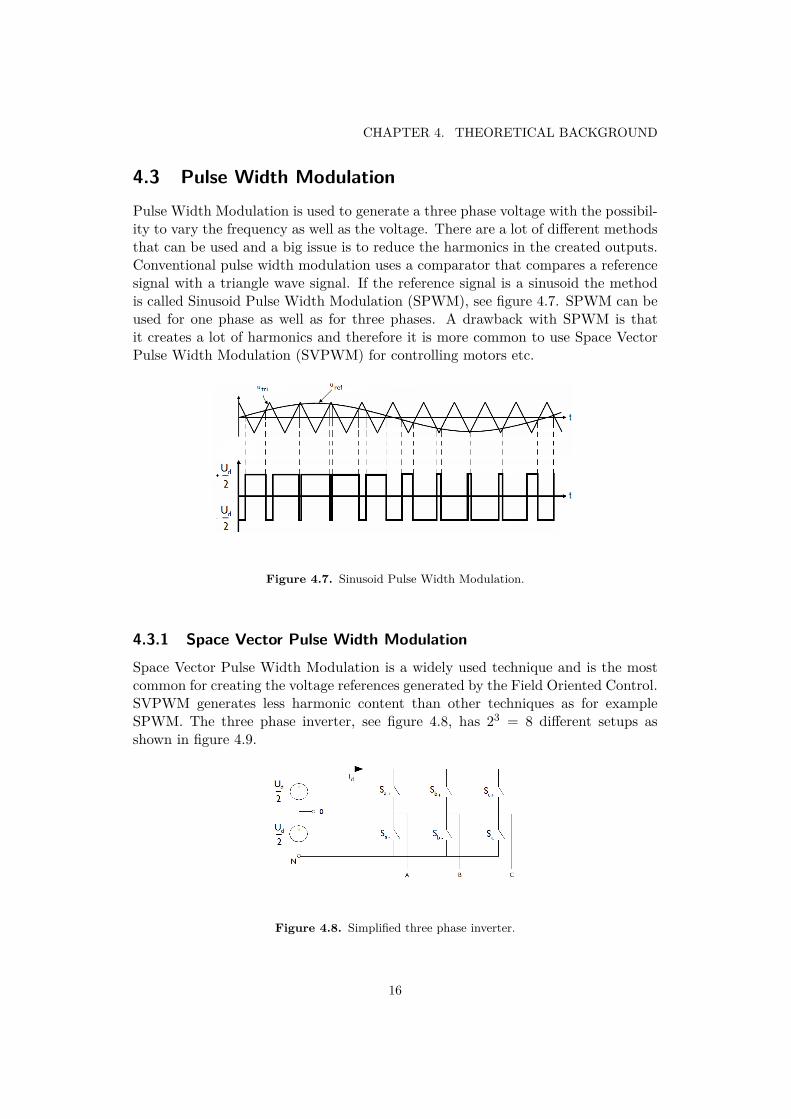
4.3 Pulse Width ModulationPulse Width Modulation is used to generate a three phase voltage with the possibil-ity to vary the frequency as well as the voltage. There are a lot of different methodsthat can be used and a big issue is to reduce the harmonics in the created outputs.Conventional pulse width modulation uses a comparator that compares a referencesignal with a triangle wave signal. If the reference signal is a sinusoid the methodis called Sinusoid Pulse Width Modulation (SPWM), see figure 4.7. SPWM can beused for one phase as well as for three phases. A drawback with SPWM is thatit creates a lot of harmonics and therefore it is more common to use Space VectorPulse Width Modulation (SVPWM) for controlling motors etc.
Figure 4.7. Sinusoid Pulse Width Modulation.
4.3.1 Space Vector Pulse Width ModulationSpace Vector Pulse Width Modulation is a widely used technique and is the mostcommon for creating the voltage references generated by the Field Oriented Control.SVPWM generates less harmonic content than other techniques as for exampleSPWM. The three phase inverter, see figure 4.8, has 23 = 8 different setups asshown in figure 4.9.
Figure 4.8. Simplified three phase inverter.
16

4.3. PULSE WIDTH MODULATION
Figure 4.9. Switching states for the three phase inverter.
17

CHAPTER 4. THEORETICAL BACKGROUND
Duty cycle calculation
From the Inverse Clarke transform comes the voltage reference vector as an input tothe SVPWM. The reference vector will land in its appropriate sector based on thesigns of the three reference voltages. An illustration is shown in figure 4.10 wherethe reference voltage vector is placed in sector one and the corresponding vectorsin the V4 and V6 directions. The vectors V0 and V7 are called zero vectors due tothat the phase to phase voltages of these two vectors are zero.
Figure 4.10. The reference voltage vector placed in sector one.
The desired stator voltage is created due to an appropriate switching pattern ofthe space vectors. To produce the voltage vector in the example the two adjacentvoltage vectors and the two zero vectors are applied during a certain amount oftime as shown in equation 4.5 where TPWM is the switching period. The generatedPWM waveform for the three phases is illustrated in 4.11. As can be seen thegenerated PWM waveform is symmetric or center aligned as this implementationminimizes the harmonic contents by reducing the switching frequency. The dutycycles for the remaining sectors are calculated in analogous way as described in theabove example.
Vref = T0V0 + T4V4 + T6V6 + T7V7TPWM
(4.5)
18

4.3. PULSE WIDTH MODULATION
Figure 4.11. The generated PWM waveform for sector one.
19


Chapter 5
Development Environment
5.1 Software5.1.1 Simulink®Simulink® from The Mathworks™ that extends MATLAB, is a high level model-based design and simulation program for embedded and dynamic systems. With itsgraphical environment and block libraries it allows implementation, simulation andtesting in an intuitive way from very simple systems to even more complex systems.The MATLAB version used in this project is R2009a.
5.1.2 Xilinx System GeneratorSystem Generator is a tool that extends Simulink for implementing algorithms in ahigh level way that automatically can be implemented into an FPGA. The versionused in this work is 11.3. Figure 5.1 shows an overview of Xilinx System Generatorwhere the different parts are explained below:
1. The System Generator block - This token always has to be in a SystemGenerator design. From the compilation options a bitstream or HDL Netlistcan be created and the target for co-simulation is set here. Clocking optionslike FPGA clock and Simulink system period are also set from this block.
2. The Simulink Library Browser - The Xilinx Blockset can be reached fromhere. All blocks like for example delays, adders, registers etc. are here to bechosen.
3. Gateway In Block - The border between the Simulink blocks and the Xilinxblocks. In the Gateway In block the sample time, the quantization by thenumber of bits and the binary point are set.
4. Gateway Out Block - Is the outer border from Xilinx blocks to Simulinkblocks. It converts Xilinx fixed point inputs into outputs of Simulink type like
21

CHAPTER 5. DEVELOPMENT ENVIRONMENT
double, float or fixed point. Specifications about I/O pin mapping can alsobe realized in this block.
5. Resource Estimator Block - This block estimates the slices, the embeddedmultipliers, flip-flops, BRAMs etc used in the design.
Figure 5.1. Xilinx System Generator overview.
An embedded design can be created with the different blocks in the XilinxBlockset. Some special blocks are worth mention for their possibility to implementblocks created of already written functions in for example VHDL or MATLABsm-code. A brief introduction of two of these blocks is found here below and moreinformation can be found in [1].
Figure 5.2. The Black Box block.
22

5.1. SOFTWARE
The Black Box block
The Black Box block, see figure 5.2, allows importing and implementing a functionwritten in VHDL or Verilog into the design. When putting the Black Box blockinto the design you are asked to chose your HDL file as *.v or *.vhd. Some specialadditions has to be done in the code before using it. For example each clock nameand clock enable name must contain the substring clk and ce respectively. Whenimporting the HDL file a configuration .m-file is created that is used in the BlackBox. It is good to know that the clock and clock enable ports are not visible on theblack box block icon.
The MCode Block
The MCode Block, see figure 5.3, passes the input values of a MALTAB functionfor evaluation in Xilinx fixed-point type. The inputs and outputs of the functionbecomes the input and output ports of the block. The m-code that the block uses istranslated in a straightforward way into equivalent behavioral VHDL/Verilog whenhardware is generated. Some design rules has to be followed when writing the m-code, for example all block inputs and outputs must be of Xilinx fixed-point typeand all blocks must at least have one output port.
Figure 5.3. The MCode block with its dialog window.
23

CHAPTER 5. DEVELOPMENT ENVIRONMENT
Figure 5.4 shows a summary of the three different implementation approachesconsidered - With pure blocks (adders, multipliers, registers etc), with a m-codefunction as a MCode block and as a Black Box created of VHDL code.
Figure 5.4. Summary of implementation approaches.
24

5.2. HARDWARE
5.2 Hardware5.2.1 Xilinx ML507 Evaluation PlatformThe ML507 Evaluation Platform used in this project, see figure 5.5, contains anFPGA from the Virtex-5 family named XC5VFX70T-1FFG1136. The board con-tains a lot of different features like for example Flash PROMs, expansion headerwith 32 single-ended I/O, 14 spare I/Os shared with buttons and LEDs, power,JTAG chain expansion capability and a 16-character x 2-line LCD display [2]. In-formation about the board’s Virtex-5 FPGA is shown in table 5.1.
Figure 5.5. Xilinx ML507 Evaluation Platform.
Slices 11 200Logic Cells 71 680
LB Flip-Flops 44 800Total Block RAM 5 328 kbits
Digital Clock Managers 12
Table 5.1. FPGA Virtex 5 XC5VFX70T-1FFG1136.
25

CHAPTER 5. DEVELOPMENT ENVIRONMENT
5.2.2 Power Board
A special designed Power Board is used containing a full three-phase inverter bridgeand two 12-bit ADCs, see figure 5.6.
Figure 5.6. Single drive inverter board.
5.2.3 Brushless DC Motor
A small brushless DC motor, figure 5.7, with a relative encoder (see section 5.2.4)is used for testing the FOC algorithm. The motor parameters are specified in table5.2.
Figure 5.7. BLDC motor 57BLS01.
5.2.4 Encoder
The encoder is of relative type which means that it shows the relative angle andnot the absolute. The connection to the resolver is made through a flat cable andthe connections are shown in figure 5.8.
26

5.2. HARDWARE
Supply voltage 36 VRated Speed 4000 rpm
Max peak current 6.8 ACont. torque at rated rpm 0.15 Nm
Resistance 1.6 ΩInductance line to line 4.3 mH
Torque constant 0.063 Nm/ABack EMF constant 6.6 V/krpm
Time constant 2.7 ms
Table 5.2. Motor parameters for 57BLS01.
Figure 5.8. The flat cable connections of the encoder.
5.2.5 Experimental SetupThe experimental setup used for testing the hardware is shown in figure 5.9. A PC(referred as number 1 in the figure) is connected to the ML507 board (number 4) bya USB platform cable (number 2). Cables with crimp contacts are then connectingthe power board (number 3) and the motor (number 5) with the ML507 board. Anadjustable power source (number 7) is also used in the setup for complementing thepower board’s 5.0 V and 3.3 V output. For testing an oscilloscope (number 6) isused. The oscilloscope is a Yokogawa DL9710L Digital oscilloscope, 5 Gs/s, 1 GHz.
27

CHAPTER 5. DEVELOPMENT ENVIRONMENT
Figure 5.9. The hardware setup in the project.
28
Chapter 6
Solution
6.1 Implementation of the different parts of the FOCalgorithm in Xilinx System Generator
For evaluating and trying the different available implementations explained in Sec-tion 5.1.2 the different parts of the Field Oriented Control algorithm are imple-mented with these different approaches. Some parts are implemented purely byblocks like for example adders, multipliers and registers, some parts by implement-ing m-code in a MCode Block and the rest with a Black Box approach. Figure6.1 shows which parts are created in what way. Why the different blocks wereimplemented in just that way is merely a random choice.
To assure a correct behavior of the different parts in the FOC algorithm everysub block is created and tested in an appropriate test bench where the outputs fromthe discrete time Xilinx blocks are compared with the outputs from the continuoustime Simulink model. An oscilloscope is also used for validation.
The obtained results are presented in chapter 7.
6.1.1 Implementation of the coordinate transformationsA test bench is built with Simulink blocks for comparison with the correspondingXilinx blocks, figure 6.2 and 6.3 shows the implementation of the Park Transform.By putting both the models together and let them have the same stimuli, in thiscase a sine wave and a saw tooth wave corresponding to the angle θ, a test benchis created, see figure 6.4. The output from the test bench is shown in figure 6.5where the similarity of the both models can be observed. The lower plot in figure6.5 shows the quantization error that occurs because of that the Simulink blocksare of continuous time and the Xilinx blocks of discrete time. Why the error isgrowing with time is due to some phase delay and that the look up tables (LUTs) inthe Xilinx blocks differs from the Simulink block’s implementation for calculatingcosine and sine of the angle θ.
29

CHAPTER 6. SOLUTION
Figure 6.1. How the different parts were implemented.
30

6.1. IMPLEMENTATION OF THE DIFFERENT PARTS OF THE FOC ALGORITHMIN XILINX SYSTEM GENERATOR
Figure 6.2. The Park Transform with Simulink blocks.
Figure 6.3. The Park transform with Xilinx blocks.
The other coordinate transformations, The Inverse Park, The Clarke and theInverse Clarke are created and tested in the same way.
31

CHAPTER 6. SOLUTION
Figure 6.4. Test Bench for the Park transformation.
32

6.1. IMPLEMENTATION OF THE DIFFERENT PARTS OF THE FOC ALGORITHMIN XILINX SYSTEM GENERATOR
Figure 6.5. Output from the Park test bench. Upper plot - Simulink (continuous),middle plot - Xilinx (Fixed point 16_13), lower plot - quantization error.
33
CHAPTER 6. SOLUTION
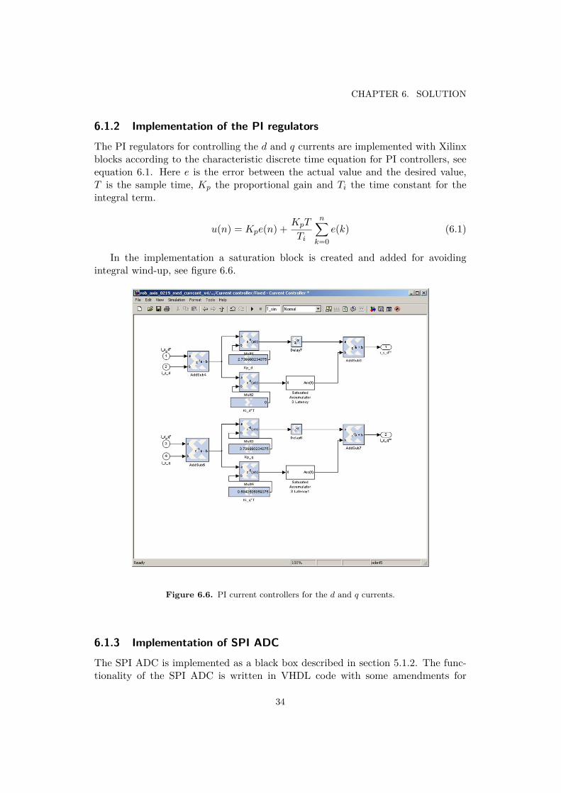
6.1.2 Implementation of the PI regulatorsThe PI regulators for controlling the d and q currents are implemented with Xilinxblocks according to the characteristic discrete time equation for PI controllers, seeequation 6.1. Here e is the error between the actual value and the desired value,T is the sample time, Kp the proportional gain and Ti the time constant for theintegral term.
u(n) = Kpe(n) + KpT
Ti
n∑k=0
e(k) (6.1)
In the implementation a saturation block is created and added for avoidingintegral wind-up, see figure 6.6.
Figure 6.6. PI current controllers for the d and q currents.
6.1.3 Implementation of SPI ADCThe SPI ADC is implemented as a black box described in section 5.1.2. The func-tionality of the SPI ADC is written in VHDL code with some amendments for
34

6.1. IMPLEMENTATION OF THE DIFFERENT PARTS OF THE FOC ALGORITHMIN XILINX SYSTEM GENERATOR
correct implementation in the black box. When the black box has created a con-figuration m-file it has to be reviewed and complemented. The implementation isshown in figure 6.7. Special input and output blocks are created and mapped withits desired I/Os on the I/O header seen to the right on the ML507 board, shownin figure 5.5. This header contains 32 single-ended signal connections to the FPGAI/Os and permits the connector to carry high-speed signals set to 2.5 or 3.3 V.
The correct functionality of the block is validated through co-simulation via aJTAG connection, known as the concept Hardware In the Loop (HIL) or FPGAin the loop, explained in section 3.4. A co-simulation block is generated from theSystem Generator block and by that the operation of the SPI ADC is validateddirectly on hardware by an oscilloscope, see figure 6.8.
Figure 6.7. The SPI ADC created as a black box and the corresponding co-simulation block.
The output from the 12-bit ADC is measured by the scopes in Simulink andconfirmed by equation 6.2. ADC_out is the output from the ADC represented by12 bits, the resistors R7 and R8, the voltages Vbus and VA are shown in figure 6.9.
BUS_SENSE = Vbus · 1R7+R8
·R8
ADC_out = BUS_SENSE · 4096VA
(6.2)
35

CHAPTER 6. SOLUTION
Figure 6.8. The output from the SPI shown on the oscilloscope during co-simulation.Top graph - Chip select, middle graph - SPI clock, bottom graph - SPI out.
Figure 6.9. Schematic figure of the ADCs.
36

6.1. IMPLEMENTATION OF THE DIFFERENT PARTS OF THE FOC ALGORITHMIN XILINX SYSTEM GENERATOR
6.1.4 Implementation of EncoderThe encoder mounted on the motor is a relative quad encoder and its reading isimplemented with a black box. First the VHDL code is written with the function-ality for the encoder and then implemented in the black box, see figure 6.10. Theoutputs from the encoder enters via the I/O header as done with the SPI ADC insection 6.1.3. The black box is tested in hardware with a co-simulation block.
Figure 6.10. The lower block is the Black Box for the encoder.
37
CHAPTER 6. SOLUTION
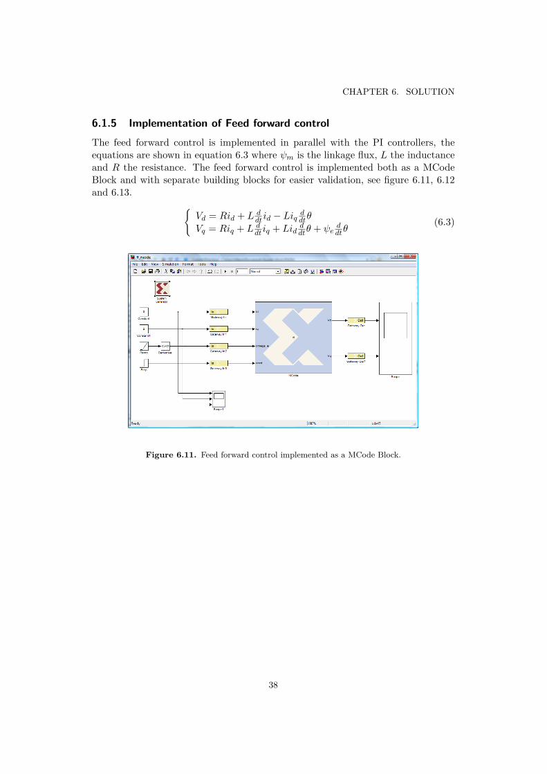
6.1.5 Implementation of Feed forward controlThe feed forward control is implemented in parallel with the PI controllers, theequations are shown in equation 6.3 where ψm is the linkage flux, L the inductanceand R the resistance. The feed forward control is implemented both as a MCodeBlock and with separate building blocks for easier validation, see figure 6.11, 6.12and 6.13.
Vd = Rid + L ddt id − Liq
ddtθ
Vq = Riq + L ddt iq + Lid
ddtθ + ψe
ddtθ
(6.3)
Figure 6.11. Feed forward control implemented as a MCode Block.
38

6.1. IMPLEMENTATION OF THE DIFFERENT PARTS OF THE FOC ALGORITHMIN XILINX SYSTEM GENERATOR
Figure 6.12. m-code for implementation of feed forward in a MCode Block.
Figure 6.13. Feed forward control implemented with blocks.
39

CHAPTER 6. SOLUTION
6.1.6 Implementation of the FOC algorithmWhen all the separate blocks in the FOC algorithm are constructed and tested theyare used for implementing the actual Field Oriented Control algorithm, as describedin section 4.1. The ready and created sub blocks are used for constituting a libraryfor further use. The FOC design after putting everything together with all the subblocks is shown in figure 6.14.
Figure 6.14. Implementation of the Field Oriented Control with Xilinx blocks.
The main issue with putting everything together is the timing analysis and thenormalization. Area estimation is also performed for the whole design by using theEstimator block.
6.1.7 Xilinx blocks vs. MCodeTo see the difference in utilized space on the FPGA between implementing a design,at one hand with blocks and on the other hand with a MCode Block, resourceestimation is done for the two different approaches. The Clarke transform is chosenas a test object because of its not to complicated composition and two test benchesare created, see figure 6.15 for the blocks and figure 6.16 for the m-code.
To implement the Clarke transformation in a MCode Block a MATLAB m-function is written. The bit representation has to be declared in the code and herethe same representation is used as within the block design.
40

6.1. IMPLEMENTATION OF THE DIFFERENT PARTS OF THE FOC ALGORITHMIN XILINX SYSTEM GENERATOR
Figure 6.15. Test bench for area estimation of the Clarke transformation.
Figure 6.16. Test bench for area estimation of the Clarke transformation imple-mented with the MCode Block.
41


Chapter 7
Results
7.1 FOC algorithm
The result after synthesizing the whole Field Oriented Control algorithm includingADCs and encoder is shown in figure 7.1.
Figure 7.1. Result after synthesizing the FOC algorithm.
Here it can be seen that 935 slices are used of the FPGA’s 11200 slices whichimplies around 8% of its capacity. The total amount of clock cycles are about 50,which with an FPGA with a clock period of 5 ns implies a frequency of 4 MHz,see figure 7.2. In this project the maximum speed is not used because of otherhardware limitations in for example the ADCs, therefore the design is clocked witha frequency of 8 kHz.
The possibility with the parallelism provided by the FPGA and by that its broadbandwidth makes it favorable to be used for implementing control of several motoraxes.
In comparison with the previous mentioned paper [5] the total number of usedslices was around 5600, which is a lot greater than the value obtained here. Thetotal control loop in [5] takes 126 clock cycles which also is greater than the hereobtained value. It has to be pointed out that the control algorithm used in [5] isnot the FOC but it gives an indication that the obtained values are good.
43

CHAPTER 7. RESULTS
Figure 7.2. Demonstration of clock cycles.
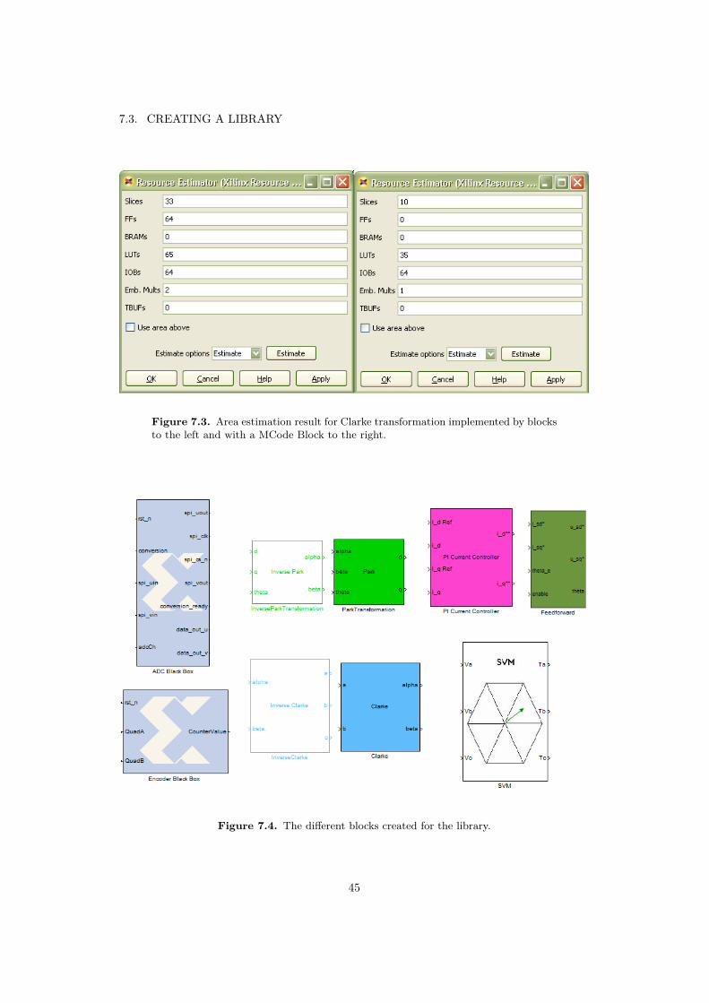
7.2 Normal blocks vs. the MCode BlockThe area estimation result for implementing the Clarke transformation by blockslike adders and multipliers versus implementing it with a MCode Block as describedin section 6.1.7 is shown in figure 7.3.
The result shows that an implementation with blocks costs 33 slices while theimplementation with a MCode block costs 10 slices. It is worth pointing out thatthis is just estimation.
7.3 Creating a libraryA library is created and the constituting different sub blocks are shown in figure7.4.
44
7.3. CREATING A LIBRARY
Figure 7.3. Area estimation result for Clarke transformation implemented by blocksto the left and with a MCode Block to the right.
Figure 7.4. The different blocks created for the library.
45


Chapter 8
Discussion
8.1 HDL and RCP
The resource estimation that is done is just an approximation and why the MCodeBlock occupies just one third of the area occupied of the blocks is hard to say. This isa problem with automated code generation, the problem of not knowing how thingsare implemented in hardware. Especially if you are dedicated and experienced withlow level programming and you know exactly how to implement it yourself withHDL code. It is worth mention that Rapid Control Prototyping and tools like thishave a big advantage because you can work with both hardware and software eventhough you are not an expert in none of the two areas. What happens and howthe design is implemented in hardware are maybe not of to much interest if youare gaining time, flexibility and get as good or quite similar results as with HDLcoding.
8.2 Xilinx System Generator and LabVIEW
Xilinx System Generator can in comparison with for example LabVIEW be seen asa more flexible program. It has a lot of features and options but with that comesa higher complexity. Sometimes the program requires input and knowledge on toolow level for being a high level program. When now having a library created theproblem of that reduces in the future, at least for this type of implementation.
8.3 Lots of parameters
An issue that occurred during the project was that several parameters had to beset in each block and by clicking on each block for changing much time was wasted.The problem was solved by creating a m-file declaring variables that were set in theblocks.
47

CHAPTER 8. DISCUSSION
8.4 Different time domainsWhen simulating the models some problems with the different time domains tookplace. This occurred because of that the FPGA has a corresponding time periodin the region of nanoseconds and the motor in milliseconds. Synchronization hadto be done and after working, testing and understanding the occurring problems itwas not an issue anymore. This is a different type of complexity that programs likeXSG has to solve for having the possibility to work in the two different regions atthe same time with the same program.
48

Chapter 9
Conclusions
9.1 Runs from SimulinkXilinx System Generator is a rather good program for Rapid Control Prototyping.The learning phase for the program is quite intense with all the features, optionsand choices in the blocks but when that threshold is reached the program has a lotof possibilities. The graphical interface is pleasant because it runs in the familiarSimulink environment. By comparing this with LabVIEW [3] it seems that XSGis harder to start with but when you are working with it and get used to it theflexibility is higher.
9.2 Easy implementationThe time saved by working with these type of high level programs is a real advantage.Also the fact that you do not have to be a hardware expert for implementing controlalgorithms in an FPGA gives a lot of possibilities. Of course one of the drawbacks byprogramming with blocks in general is that the code is not optimized and debuggingin a design with a lot of blocks is relatively time consuming and an error is sometimesvery hard to find. With normal written code an error can be seen more easilybecause it is not hidden in a block. This is although always a subjective thingbecause it depends on for example your proper experience.
9.3 ParallelismThe parallelism in an FPGA is a great advantage for algorithms and problems thatcan be implemented and solved in parallel. The parallelism and the speed of theFPGA lead to a higher bandwidth and that is why an FPGA is suitable for motorcontrol with several axes like in for example robotic and mechatronic systems. Theadvantage of programming tasks in parallel instead of in series is that a change orreplacement of a task can be done in an easier way without affecting other tasks.
49

Chapter 10
Future work
Possible extensions and future work is always an interesting part in this type of in-vestigation projects. A natural continuation is to optimize the blocks and algorithmby area and time. The next step would be implementation of several motors. Pos-sible extensions would be implementing other control algorithms and modulationtechniques. In general:
• Optimize controllers and blocks.
• Optimize speed and area.
• Implement dead-time bands for SVPWM.
• Implement other modulation techniques.
• Implement interfaces to different measurement systems.
• Generic approach to motor control.
• Interfaces to an external control other than Simulink.
• Further implementation with several motors.
• Comparison between XSG generated code and hand written code respecting.- Time of implementation.- Area and speed.
• Implement other control algorithms.
51


Bibliography
[1] Xilinx system generator user guide. Website, December 2009. http://www.xilinx.com/support/documentation/sw_manuals/xilinx11/sysgen_user.pdf.
[2] Xilinx ug347 ml505/ml506/ml507 evaluation platform user guide. Website, Oc-tober 2009. http://www.xilinx.com/support/documentation/boards_and_kits/ug347.pdf.
[3] Magnus Fredrixon. Evaluation of a system for rapid control prototyping in thefield of robot control. Technical report, ABB Corporate Research, Sweden, 2009.
[4] Eike Husing. Rapid control prototyping with labview fpga. Technical ReportSECRC/AT/TR-2009/040, ABB Corporate Research, Sweden, 2009.
[5] Stéphane Simard, Rachid Beguenane, and Jean-Gabriel Mailloux. Performanceevaluation of rotor flux-oriented control on fpga for advanced ac drives. Journalof Robotics and Mechatronics, 21(1):113–120, 2009. http://www.fujipress.jp/finder/xslt.php?mode=present&inputfile=ROBOT002100010014.xml.
53