Embed Size (px)
Citation preview
Caliber Interconnect SolutionsDesign for perfection
Case Study Package Design &
SI/PI analysis
Caliber Interconnect Solutions (Pvt) LtdNo 9 B/1 , Poombukar Nagar, Thudiyalur,Coimbatore- 641034. Tamil Nadu, India.www.caliberinterconnect.com
Caliber Interconnect Solutions Pvt Ltd1
Mission & Vision
Mission
Vision
Quality Policy
“CALIBER INTERCONNECT SOLUTIONS PRIVATE LIMITED iscommitted to meet and exceed customers expectations through timely delivery of cost effective quality designs through ever improving process and team work.”
2Caliber Interconnect Solutions Pvt Ltd
“Developing and applying technological solutions to the benefits of the society that will not affect the safetyand living standards of our future generations.”
“Provide dependable solutions to the satisfaction of the customers through intensive R&D and proven quality control procedures using disciplined workforce.”
Profile
Leading provider of high speed design and analysis services for Probe Cards System in Packages (SiP) Multi Layer Package Designs and Layouts Multi Chip Modules(MCMs) MLO/MLC Substrate Designs
Highly Skilled Design/Analysis and Layout Team More than 200+ package designs successfully completed Organic build up from 1-2-1 to 8-2-8 layers Low Cost 4 layer Laminates Multi layer Ceramic designs Experience in wirebond and flip chip design and layout techniques Chip Scale Package designs
Cost Effective and Timely Job completion- Lead Time 1.5 weeks to 3 weeks from frozen netlist based on complexity
3Caliber Interconnect Solutions Pvt Ltd
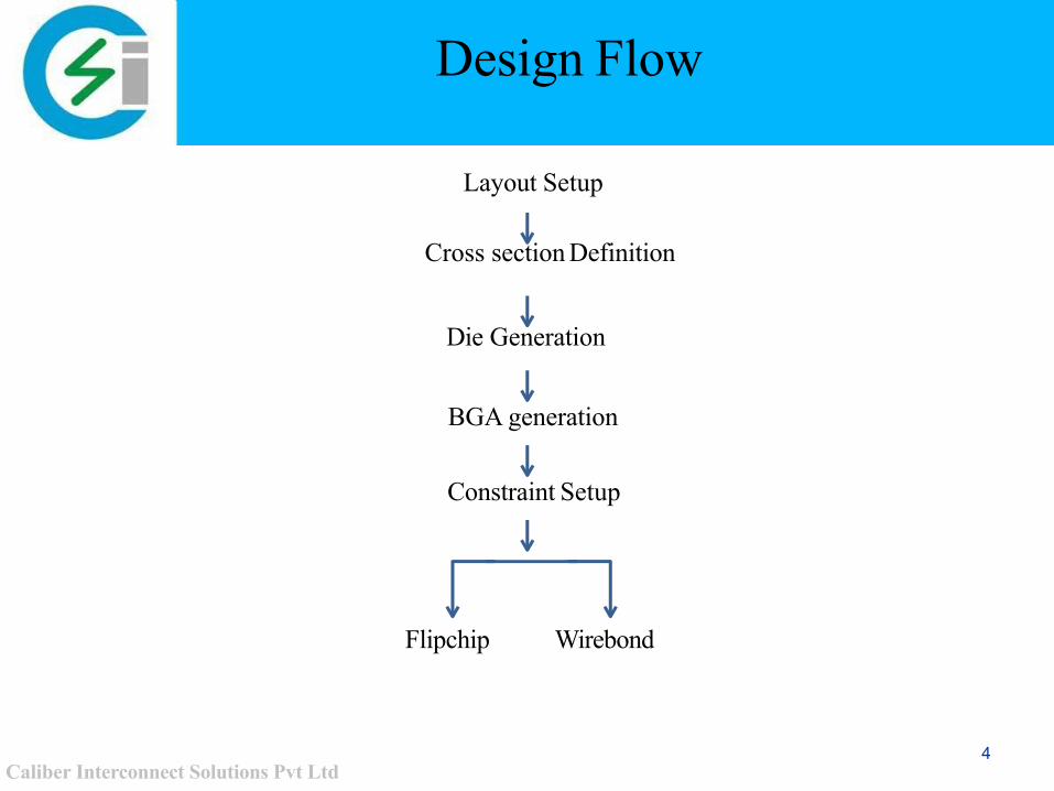
Layout Setup
Cross section Definition
Die Generation
BGA generation
Constraint Setup
Flipchip Wirebond
Design Flow
4Caliber Interconnect Solutions Pvt Ltd
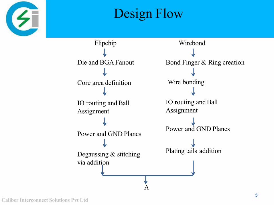
Flipchip
Die and BGA Fanout
Core area definition
IO routing and Ball Assignment
Power and GND Planes
Degaussing & stitching via addition
Wirebond
Bond Finger & Ring creation
Wire bonding
IO routing and Ball Assignment
Power and GND Planes
Plating tails addition
A
Design Flow
5Caliber Interconnect Solutions Pvt Ltd
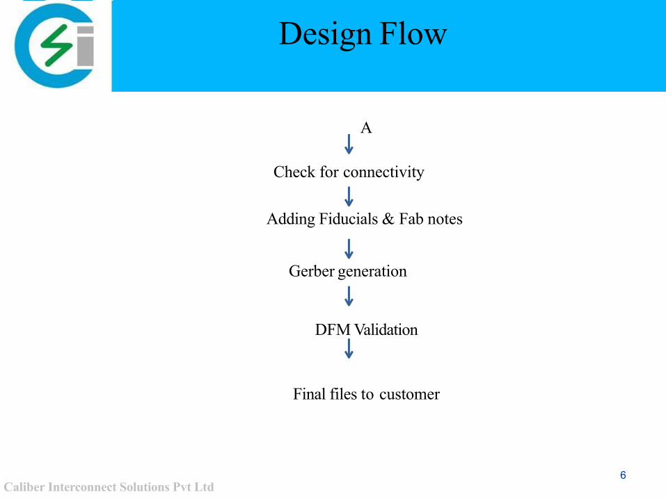
A
Check for connectivity
Adding Fiducials & Fab notes
Gerber generation
DFM Validation
Final files to customer
Design Flow
6Caliber Interconnect Solutions Pvt Ltd
Design Examples
7Caliber Interconnect Solutions Pvt Ltd
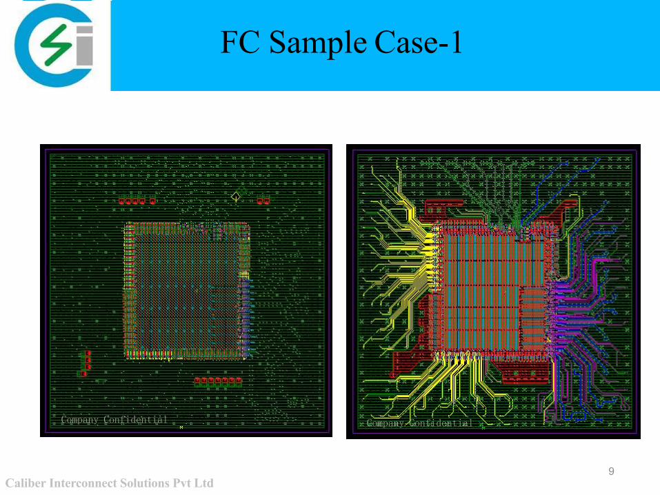
FC Sample Case-1
8Caliber Interconnect Solutions Pvt Ltd
Die Pin Count: 5043 die pins
Bump Pitch: 180um
Package size: 33x33 mm
BGA array: 32x32 with 1 mm pitch
Key Design attributes
196 Ios with different interfaces like DDR, SerDes and LVDS
All the signals routed in 2 layers and SerDes Tx and RX signals routed in different layers
Solid GND plane provided as reference for SerDes & Power planes for LVDS and DDR signals
Stitching vias added for SerDes with equal spacing between vias from start to end of the routing2 critical power pins spread out equally in core area of the Die and fanout of core area was
challenging and 0201 capacitors added in Die side for critical power
Length matching done as per the skew given
Layers used – 4-2-4 structure (BU-C-BU)
Lead Time – 2.5 weeks
FC Sample Case-1
9Caliber Interconnect Solutions Pvt Ltd
Company Confidential Company Confidential
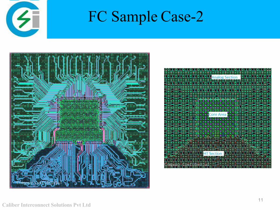
FC Sample Case-2
10Caliber Interconnect Solutions Pvt Ltd
Die Pin Count: 3302 die pins
Bump Pitch: 180um
Package size: 45x45 mm
BGA array: 44x44 with 1 mm pitch
Key Design attributes
77 signals of 50 ohms, 85 differential pairs in HT section and 243 pairs in Analog sectionAll the pairs are routed in 2 layers and maximum spacing maintained between the pairs to allow
GND flow between the pairs
Stitching vias added between the pairs with equal spacing from start to end of the routingFor each power and GND balls in core area, maximum number of vias added to improve
connection path between Die and BGA
Differential pair P and N balls have given a common large oval void area to avoid sharp corners.
HT signals are matched within 7ps tolerance
Layers used – 4-2-4 structure (BU-C-BU) & Lead Time – 2 weeks
FC Sample Case-2
11Caliber Interconnect Solutions Pvt Ltd
Company Confidential
Company Confidential
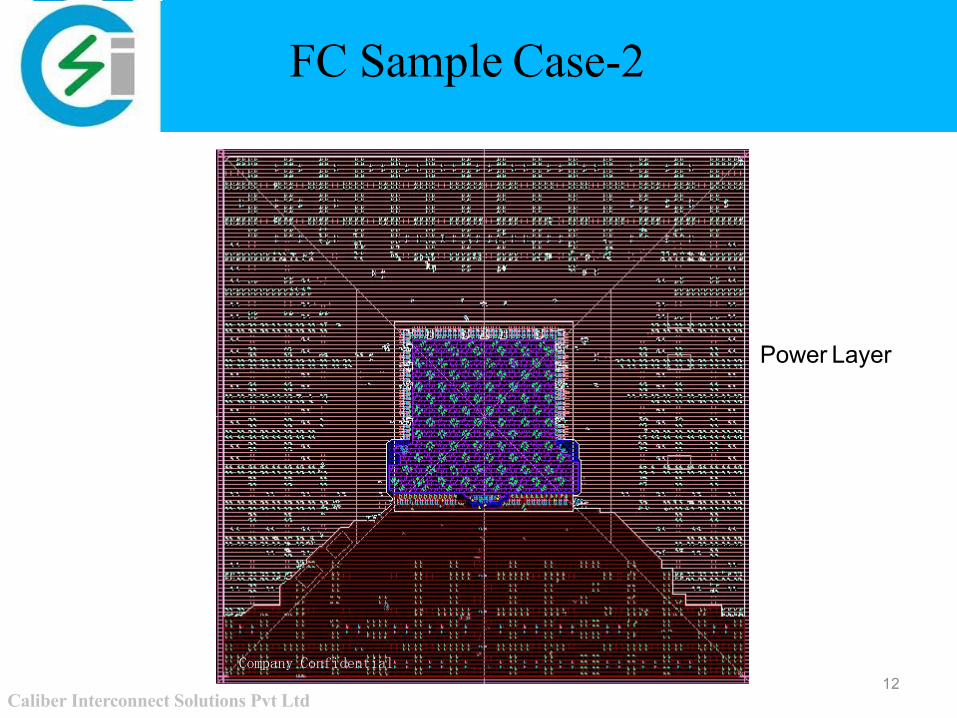
FC Sample Case-2
Power Layer
12Caliber Interconnect Solutions Pvt Ltd
Company Confidential
FC Sample Case-3
13Caliber Interconnect Solutions Pvt Ltd
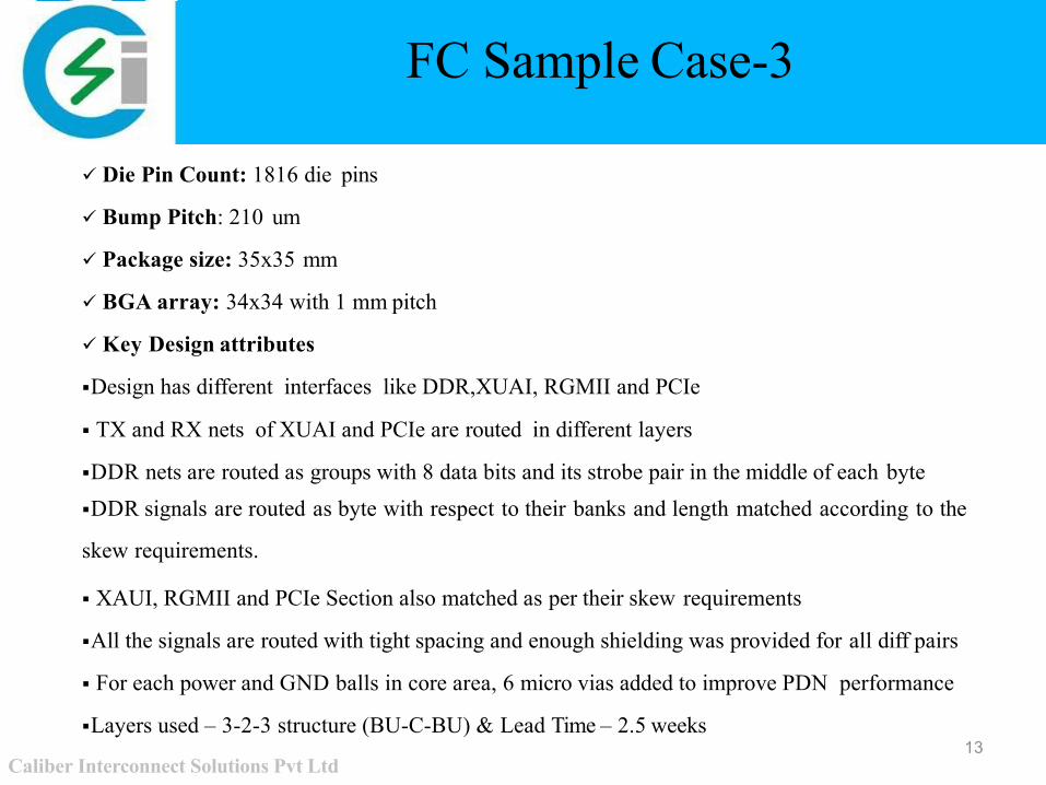
Die Pin Count: 1816 die pins
Bump Pitch: 210 um
Package size: 35x35 mm
BGA array: 34x34 with 1 mm pitch
Key Design attributes
Design has different interfaces like DDR,XUAI, RGMII and PCIe
TX and RX nets of XUAI and PCIe are routed in different layers
DDR nets are routed as groups with 8 data bits and its strobe pair in the middle of each byteDDR signals are routed as byte with respect to their banks and length matched according to the
skew requirements.
XAUI, RGMII and PCIe Section also matched as per their skew requirements
All the signals are routed with tight spacing and enough shielding was provided for all diff pairs
For each power and GND balls in core area, 6 micro vias added to improve PDN performance
Layers used – 3-2-3 structure (BU-C-BU) & Lead Time – 2.5 weeks
FC Sample Case-3
14Caliber Interconnect Solutions Pvt Ltd
Company Confidential
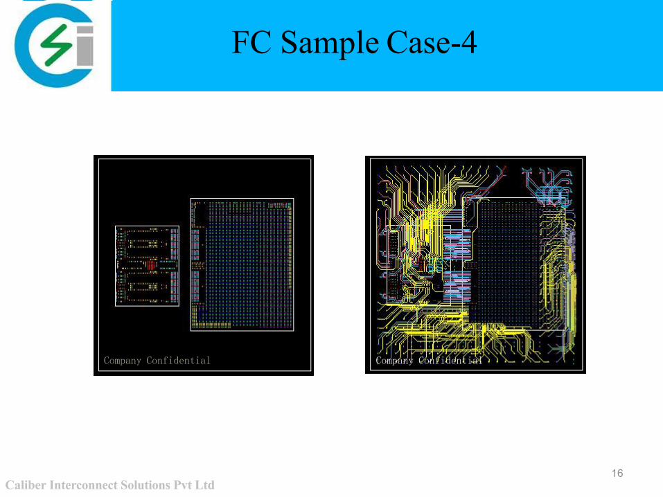
FC Sample Case-4
15Caliber Interconnect Solutions Pvt Ltd
Die Pin Count: DIE1 - 2335 pins, DIE2 - 692
Bump Pitch: DIE1- 400 um, DIE2 – 180um
Package size: CBGA 25x25 mm
BGA array: 24x24 with 1 mm pitch
Key Design attributes
Multi chip flip chip design with 2 DIE in a single substrate
One die is analog & another is digital & connectivity achieved between 2 DIE using diff pairs
192 differential pairs in digital section and 188 pairs in analog section
Design consists of XAUI and GPIO Section and they are routed per their routing specification.Analog and digital power/GNDs are properly planned and plane pouring is done without
interference of each other
Core area of Digital DIE have different powers and achieving connectivity was difficult task
Layers used – 12 layers and Lead Time – 3 weeks
FC Sample Case-4
16Caliber Interconnect Solutions Pvt Ltd
Company Confidential Company Confidential
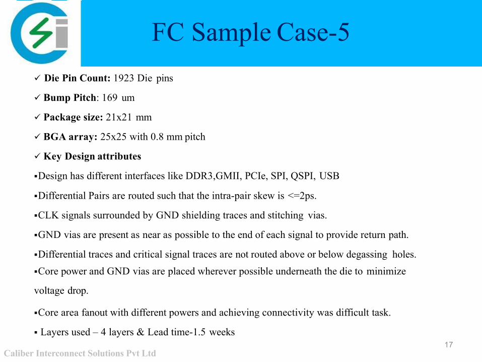
FC Sample Case-5
17Caliber Interconnect Solutions Pvt Ltd
Die Pin Count: 1923 Die pins
Bump Pitch: 169 um
Package size: 21x21 mm
BGA array: 25x25 with 0.8 mm pitch
Key Design attributes
Design has different interfaces like DDR3,GMII, PCIe, SPI, QSPI, USB
Differential Pairs are routed such that the intra-pair skew is <=2ps.
CLK signals surrounded by GND shielding traces and stitching vias.
GND vias are present as near as possible to the end of each signal to provide return path.
Differential traces and critical signal traces are not routed above or below degassing holes.Core power and GND vias are placed wherever possible underneath the die to minimize
voltage drop.
Core area fanout with different powers and achieving connectivity was difficult task.
Layers used – 4 layers & Lead time-1.5 weeks
FC Sample Case-5
COMPLEX CORE AREA
18Caliber Interconnect Solutions Pvt Ltd
Company Confidential Company Confidential
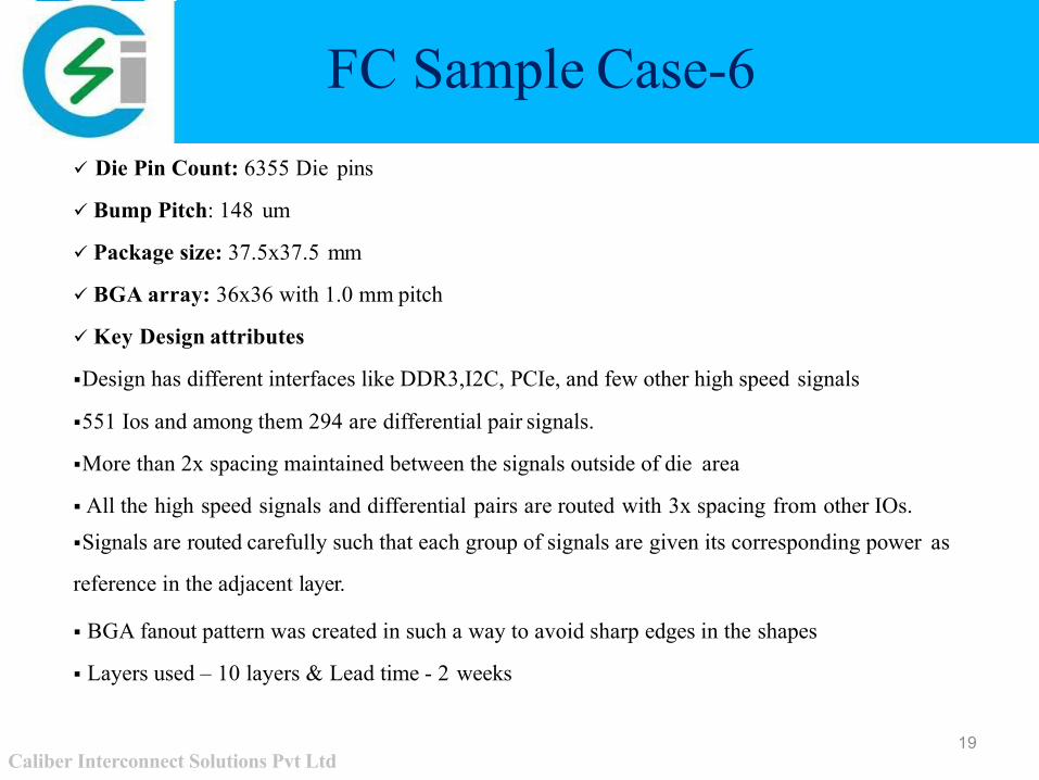
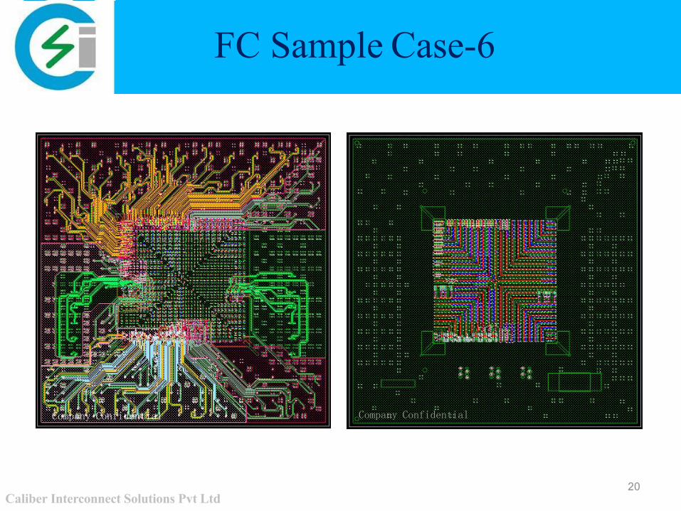
FC Sample Case-6
19Caliber Interconnect Solutions Pvt Ltd
Die Pin Count: 6355 Die pins
Bump Pitch: 148 um
Package size: 37.5x37.5 mm
BGA array: 36x36 with 1.0 mm pitch
Key Design attributes
Design has different interfaces like DDR3,I2C, PCIe, and few other high speed signals
551 Ios and among them 294 are differential pair signals.
More than 2x spacing maintained between the signals outside of die area
All the high speed signals and differential pairs are routed with 3x spacing from other IOs.Signals are routed carefully such that each group of signals are given its corresponding power as
reference in the adjacent layer.
BGA fanout pattern was created in such a way to avoid sharp edges in the shapes
Layers used – 10 layers & Lead time - 2 weeks
FC Sample Case-6
20Caliber Interconnect Solutions Pvt Ltd
Company Confidential Company Confidential
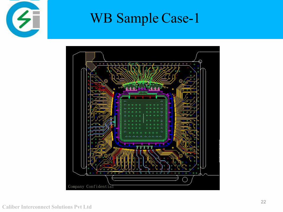
WB Sample Case-1
21Caliber Interconnect Solutions Pvt Ltd
Die Pin Count: 689 die pins in 2 rows
Package size: 31x31 mm
BGA array: 1289 ball pins with 1 mm pitch
Key Design attributes
241 Ios with different interfaces like DDR,GPIO,I2C,SPI,USB and others
Differential pairs are routed with 5x spacing to other signals
GND shielding traces added on both sides of critical signals
Each group of signals is routed with its corresponding GND reference in GND layer
Power rings created for 4 powers and 2 GND.
Layers used – 4 layers
Lead Time – 1.5 weeks
WB Sample Case-1
22Caliber Interconnect Solutions Pvt Ltd
Company Confidential
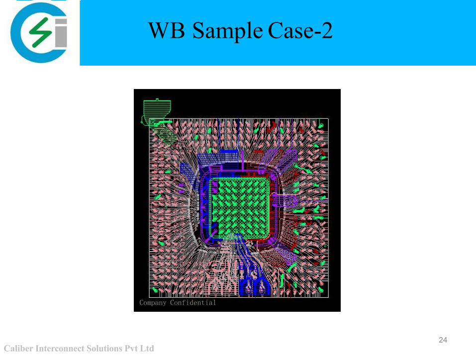
WB Sample Case-2
23Caliber Interconnect Solutions Pvt Ltd
Die Pin Count: 292 die pins
Package size: 27x27 mm
BGA array: 484 pin perimeter matrix BGA with 1 mm pitch
Key Design attributes
316 Ios with different interfaces like DDR,GMII,MII,GPIO and other interfacesRouting done in any angle trace to reduce length and to increase space for routing all signals in
Top layer
TX and RX pairs are routed with their respective GND shielding traces on both sides of the pairs
and the same GND is given as reference in immediate next layer
Due to spacing constraints, 2nd row of bond finger is created for few signals and connected to
nearest ball pin.
Power ring created for 3 different powers and vias are connected to its power plane.
Plating tails added for all nets
Layers used – 4 layers and Lead Time – 2 weeks
WB Sample Case-2
24Caliber Interconnect Solutions Pvt Ltd
Company Confidential
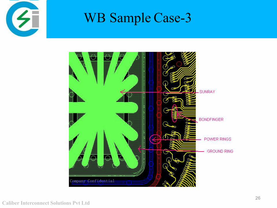
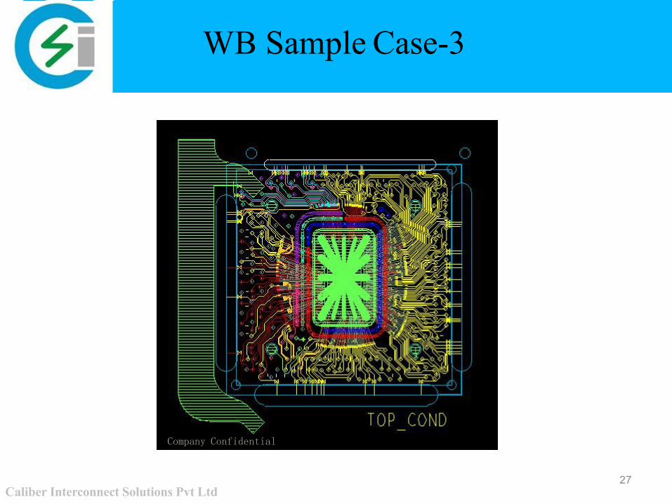
WB Sample Case-3
25Caliber Interconnect Solutions Pvt Ltd
Die Pin Count: 365 die pins
Package size: 21x21 mm
BGA array: 365 pin perimeter matrix HSBGA with 1 mm pitch
Key Design attributes
226 Ios with Analog, Digital and HDMI section and among them 4 are differential pairs in HDMI
All the signals are routed in Top layer with its respective GND as reference
Staggered Bond finger pattern created for signals and few power and GND pins
4 Power rings created for 5 powers and 3 GND nets.
Sunray pattern added to core ground ring
Plating tails added for all nets
Fiducials placed as per requirement and connected to GND
Layers used – 4 layers
Lead Time – 2 weeks
WB Sample Case-3
26Caliber Interconnect Solutions Pvt Ltd
Company Confidential
WB Sample Case-3
27Caliber Interconnect Solutions Pvt Ltd
Company Confidential
PACKAGE SI & PI SIMULATION
28Caliber Interconnect Solutions Pvt Ltd
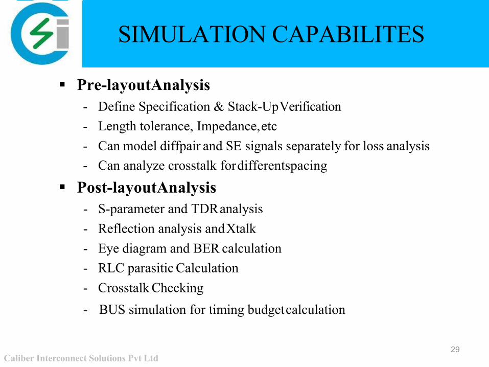
SIMULATION CAPABILITES
29Caliber Interconnect Solutions Pvt Ltd
Pre-layoutAnalysis- Define Specification & Stack-Up Verification- Length tolerance, Impedance, etc- Can model diffpair and SE signals separately for loss analysis- Can analyze crosstalk for differentspacing
Post-layoutAnalysis- S-parameter and TDR analysis- Reflection analysis and Xtalk- Eye diagram and BER calculation- RLC parasitic Calculation- Crosstalk Checking- BUS simulation for timing budget calculation
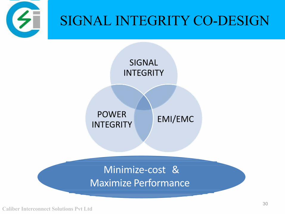
SIGNAL INTEGRITY CO-DESIGN
SIGNAL INTEGRITY
EMI/EMCPOWER INTEGRITY
Minimize-cost & Maximize Performance
30Caliber Interconnect Solutions Pvt Ltd
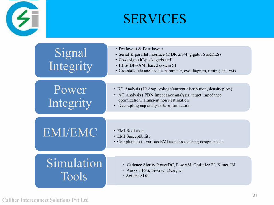
SERVICES
• Pre layout & Post layout• Serial & parallel interface (DDR 2/3/4, gigabit-SERDES)• Co-design (IC/package/board)• IBIS/IBIS-AMI based system SI• Crosstalk, channel loss, s-parameter, eye-diagram, timing analysis
• DC Analysis (IR drop, voltage/current distribution, density plots)• AC Analysis ( PDN impedance analysis, target impedance
optimization, Transient noise estimation)• Decoupling cap analysis & optimization
Signal Integrity
Power Integrity
• EMI Radiation• EMI Susceptibility• Compliances to various EMI standards during design phase
EMI/EMC
• Cadence Sigrity PowerDC, PowerSI, Optimize PI, Xtract IM• Ansys HFSS, Siwave, Designer• Agilent ADS
Simulation Tools
31Caliber Interconnect Solutions Pvt Ltd
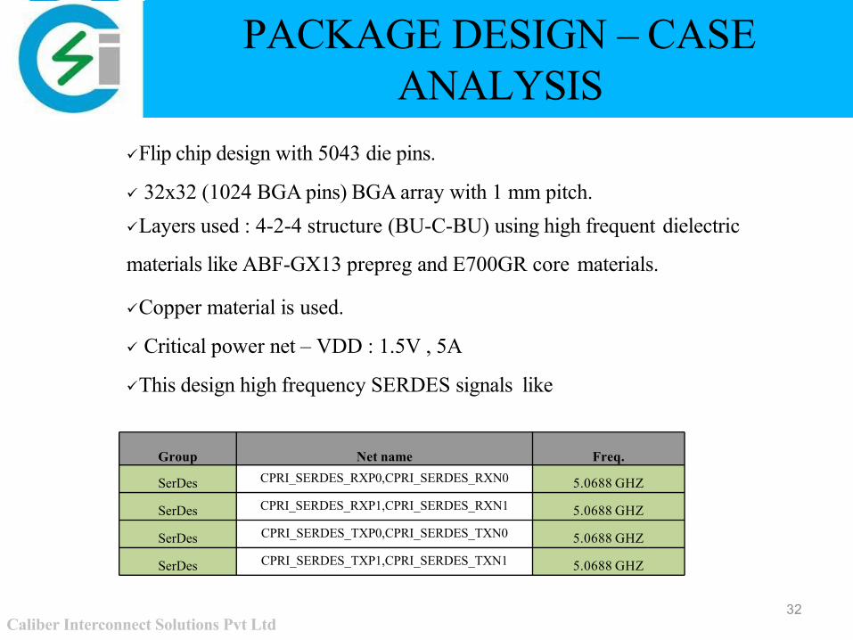
PACKAGE DESIGN – CASE ANALYSIS
32Caliber Interconnect Solutions Pvt Ltd
Flip chip design with 5043 die pins.
32x32 (1024 BGA pins) BGA array with 1 mm pitch.Layers used : 4-2-4 structure (BU-C-BU) using high frequent dielectric
materials like ABF-GX13 prepreg and E700GR core materials.
Copper material is used.
Critical power net – VDD : 1.5V , 5A
This design high frequency SERDES signals like
Group Net name Freq.
SerDes CPRI_SERDES_RXP0,CPRI_SERDES_RXN0 5.0688 GHZ
SerDes CPRI_SERDES_RXP1,CPRI_SERDES_RXN1 5.0688 GHZ
SerDes CPRI_SERDES_TXP0,CPRI_SERDES_TXN0 5.0688 GHZ
SerDes CPRI_SERDES_TXP1,CPRI_SERDES_TXN1 5.0688 GHZ
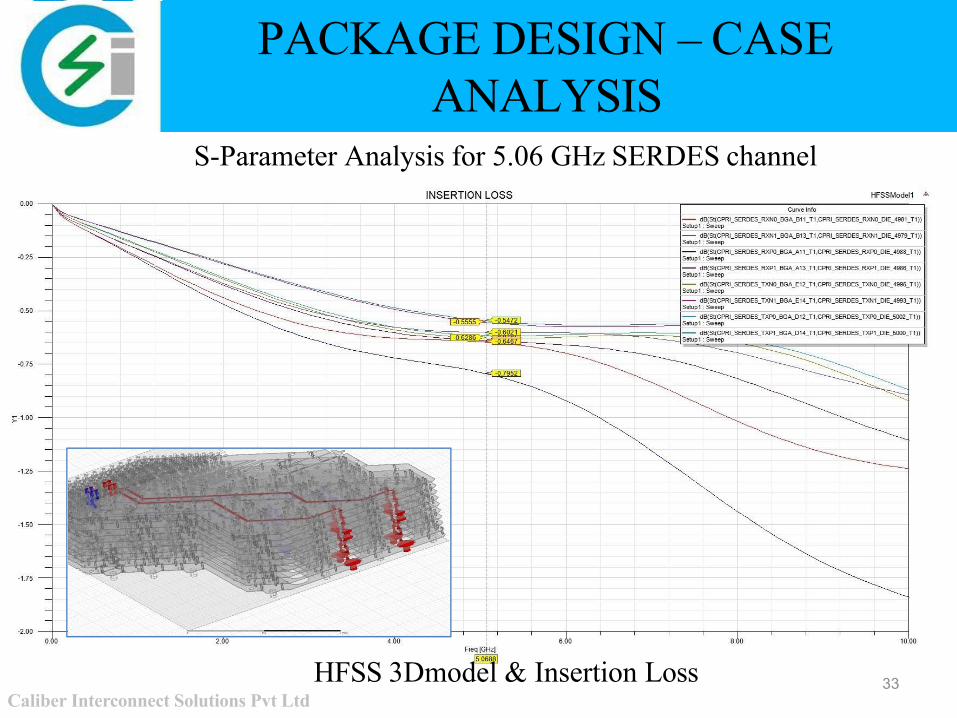
S-Parameter Analysis for 5.06 GHz SERDES channel
PACKAGE DESIGN – CASE ANALYSIS
HFSS 3Dmodel & Insertion LossCaliber Interconnect Solutions Pvt Ltd
33
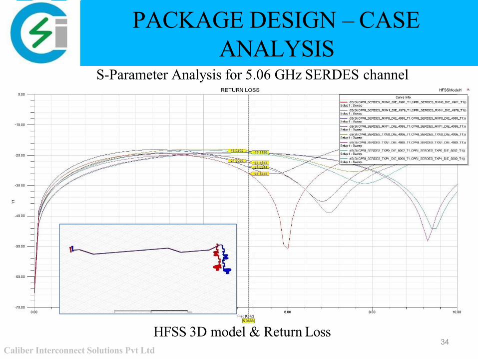
PACKAGE DESIGN – CASE ANALYSIS
S-Parameter Analysis for 5.06 GHz SERDES channel
34 HFSS 3D model & Return Loss
Caliber Interconnect Solutions Pvt Ltd
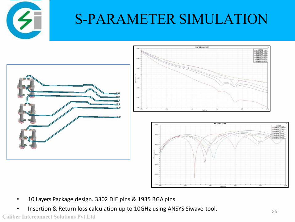
S-PARAMETER SIMULATION
• 10 Layers Package design. 3302 DIE pins & 1935 BGA pins• Insertion & Return loss calculation up to 10GHz using ANSYS Siwave tool. 35
Caliber Interconnect Solutions Pvt Ltd
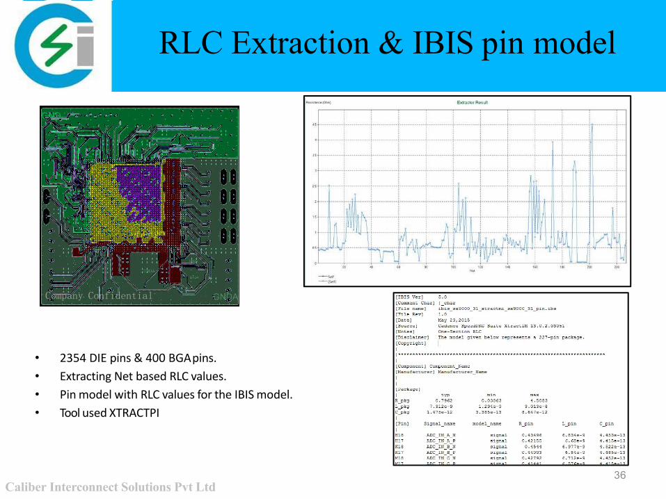
RLC Extraction & IBIS pin model
• 2354 DIE pins & 400 BGA pins.• Extracting Net based RLC values.• Pin model with RLC values for the IBIS model.• Tool used XTRACTPI
36Caliber Interconnect Solutions Pvt Ltd
Company Confidential
POWER INTEGRITY ANALYSIS
37Caliber Interconnect Solutions Pvt Ltd
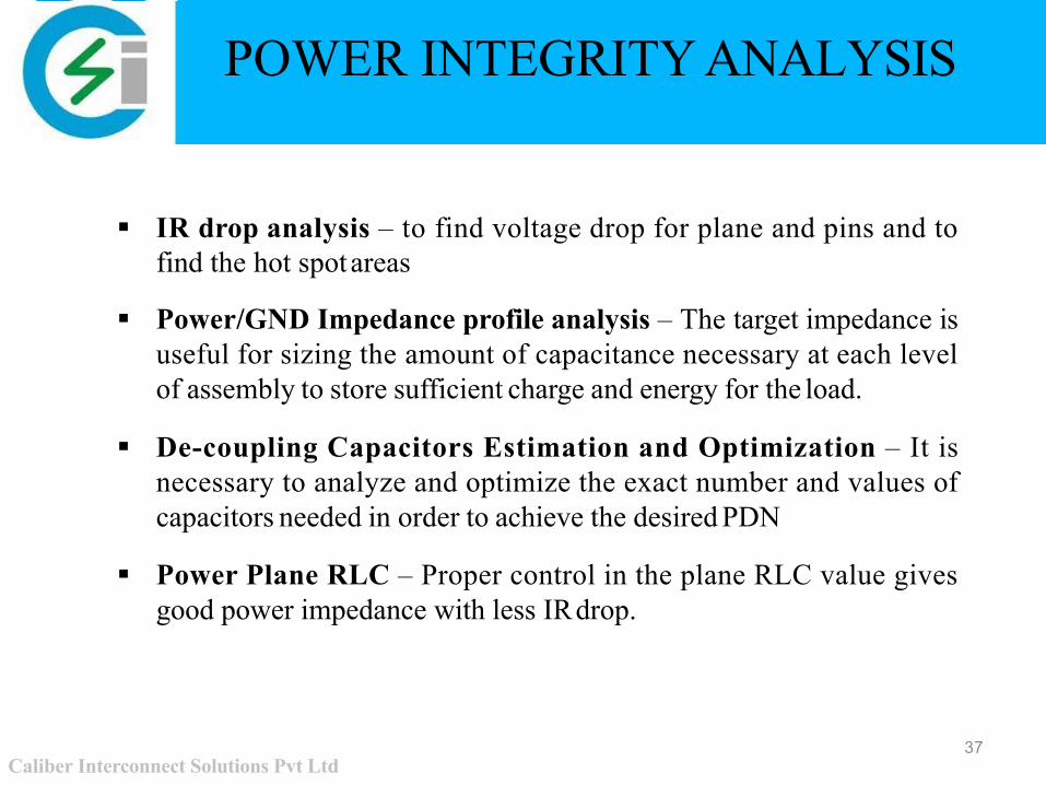
IR drop analysis – to find voltage drop for plane and pins and to find the hot spot areas
Power/GND Impedance profile analysis – The target impedance is useful for sizing the amount of capacitance necessary at each level of assembly to store sufficient charge and energy for the load.
De-coupling Capacitors Estimation and Optimization – It is necessary to analyze and optimize the exact number and values of capacitors needed in order to achieve the desired PDN
Power Plane RLC – Proper control in the plane RLC value gives good power impedance with less IR drop.
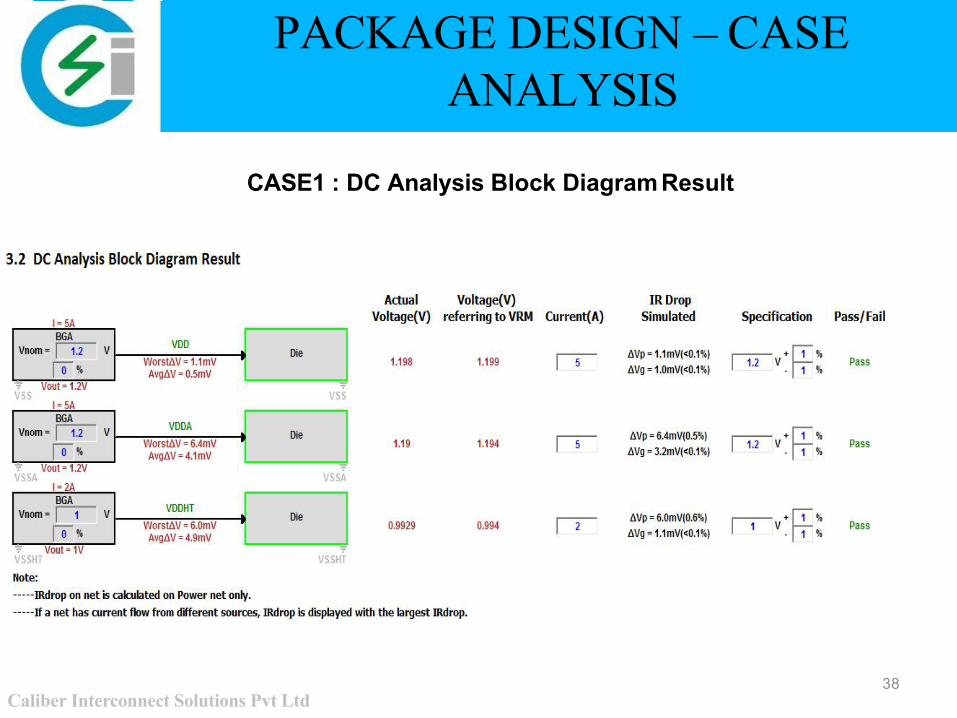
CASE1 : DC Analysis Block Diagram Result
PACKAGE DESIGN – CASE ANALYSIS
38Caliber Interconnect Solutions Pvt Ltd
PACKAGE DESIGN – CASE ANALYSIS
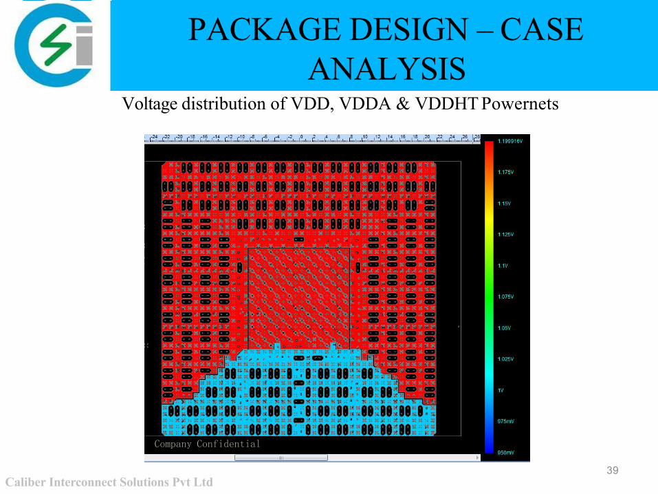
Voltage distribution of VDD, VDDA & VDDHT Powernets
DDRVDDQ Voltage distribution plot
39Caliber Interconnect Solutions Pvt Ltd
Company Confidential
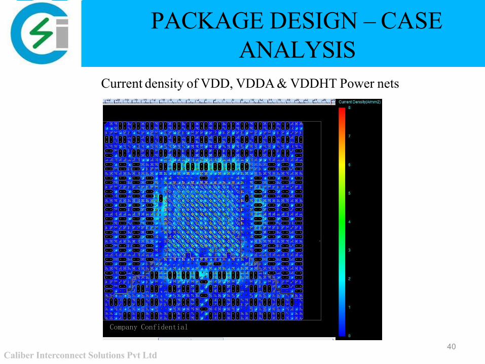
Current density of VDD, VDDA & VDDHT Power nets
PACKAGE DESIGN – CASE ANALYSIS
40Caliber Interconnect Solutions Pvt Ltd
Company Confidential
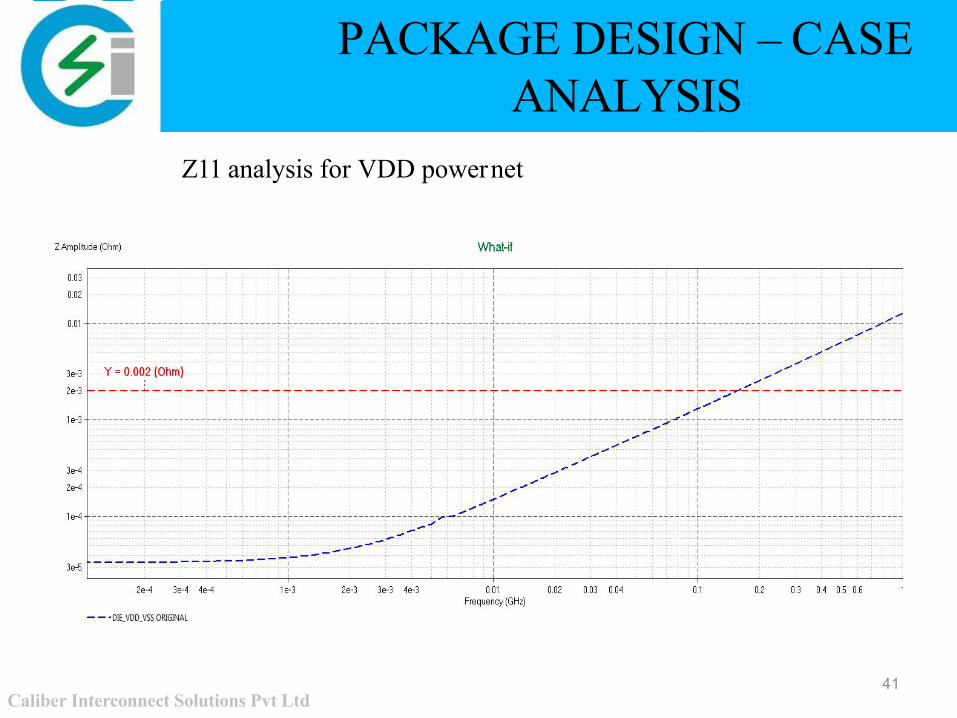
Z11 analysis for VDD power net
PACKAGE DESIGN – CASE ANALYSIS
41Caliber Interconnect Solutions Pvt Ltd
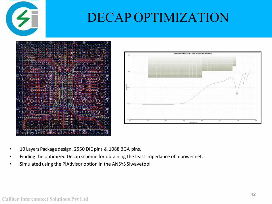
DECAP OPTIMIZATION
• 10 Layers Package design. 2550 DIE pins & 1088 BGA pins.• Finding the optimized Decap scheme for obtaining the least impedance of a power net.• Simulated using the PiAdvisor option in the ANSYS Siwavetool
42Caliber Interconnect Solutions Pvt Ltd
Company Confidential
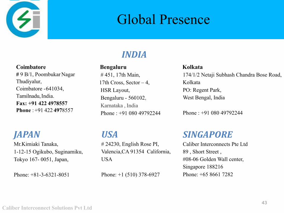
Our Locations
Coimbatore# 9 B/1, Poombukar NagarThudiyalur,Coimbatore - 641034,Tamilnadu, India.Fax: +91 422 4978557Phone : +91 422 4978557
USA# 24230, English Rose PI, Valencia,CA 91354 California,USA
Phone: +1 (510) 378-6927
Caliber Interconnect Solutions Pvt Ltd
Bengaluru # 451, 17th Main, 17th Cross, Sector – 4, HSR Layout, Bengaluru - 560102, Karnataka , India Phone : +91 080 49792244
INDIA
SINGAPORECaliber Interconnects Pte Ltd89 , Short Street ,#08-06 Golden Wall center,Singapore 188216Phone: +65 8661 7282
Kolkata174/1/2 Netaji Subhash Chandra Bose Road, KolkataPO: Regent Park,West Bengal, India
Phone : +91 080 49792244
JAPANMr.Kimiaki Tanaka,1-12-15 Ogikubo, Suginamiku,Tokyo 167- 0051, Japan,
Phone: +81-3-6321-8051
Global Presence
43

THANK YOU !!!
Contact us [email protected]
Visit us at www.caliberinterconnect.com
Caliber Interconnect Solutions Pvt Ltd
Thank You
44