Embed Size (px)
Citation preview
IEEE TRANSACTIONS ON INDUSTRIAL ELECTRONICS, VOL. 60, NO. 2, FEBRUARY 2013 523
Cascade Cockcroft–Walton Voltage MultiplierApplied to Transformerless High
Step-Up DC–DC ConverterChung-Ming Young, Member, IEEE, Ming-Hui Chen, Student Member, IEEE,
Tsun-An Chang, Chun-Cho Ko, and Kuo-Kuang Jen
Abstract—This paper proposes a high step-up dc-dc converterbased on the Cockcroft-Walton (CW) voltage multiplier without astep-up transformer. Providing continuous input current with lowripple, high voltage ratio, and low voltage stress on the switches,diodes, and capacitors, the proposed converter is quite suitablefor applying to low-input-level dc generation systems. More-over, based on the n-stage CW voltage multiplier, the proposedconverter can provide a suitable dc source for an n + 1-levelmultilevel inverter. In this paper, the proposed control strategyemploys two independent frequencies, one of which operates athigh frequency to minimize the size of the inductor while the otherone operates at relatively low frequency according to the desiredoutput voltage ripple. A 200-W laboratory prototype is built fortest, and both simulation and experimental results demonstratethe validity of the proposed converter.
Index Terms—Cockcroft–Walton (CW) voltage multiplier, highvoltage ratio, multilevel inverter, step-up dc–dc converter.
I. INTRODUCTION
IN RECENT YEARS, extensive use of electrical equipmenthas imposed severe demands for electrical energy, and this
trend is constantly growing. Consequently, researchers andgovernments worldwide have made efforts on renewable energyapplications for mitigating natural energy consumption andenvironmental concerns [1], [2]. Among various renewableenergy sources, the photovoltaic (PV) cell and fuel cell havebeen considered attractive choices [3]–[5]. However, withoutextra arrangements, the output voltages generated from bothof them are with rather low level [6], [7]. Thus, a high step-up dc-dc converter is desired in the power conversion systemscorresponding to these two energy sources. In addition to thementioned applications, a high step-up dc-dc converter is alsorequired by many industrial applications, such as high-intensity
Manuscript received March 5, 2011; revised August 4, 2011 andNovember 19, 2011; accepted January 14, 2012. Date of publicationFebruary 16, 2012; date of current version September 13, 2012. This workwas supported by the National Science Council of Taiwan under Project NSC100-2221-E-011-009.
C.-M. Young, M.-H. Chen, T.-A. Chang, and C.-C. Ko are with the De-partment of Electrical Engineering, National Taiwan University of Scienceand Technology, Taipei 10673, Taiwan (e-mail: [email protected];[email protected]; [email protected]; [email protected]).
K.-K. Jen is with Chung-Shan Institute of Science and Technology, Taoyuan325, Taiwan (e-mail: [email protected]).
Color versions of one or more of the figures in this paper are available onlineat http://ieeexplore.ieee.org.
Digital Object Identifier 10.1109/TIE.2012.2188255
discharge lamp ballasts for automobile headlamps and batterybackup systems for uninterruptible power supplies [8].
Theoretically, the conventional boost dc-dc converter canprovide a very high voltage gain by using an extremely highduty cycle. However, practically, parasitic elements associatedwith the inductor, capacitor, switch, and diode cannot be ig-nored, and their effects reduce the theoretical voltage gain [9].Up to now, many step-up dc-dc converters have been proposedto obtain high voltage ratios without extremely high duty cycleby using isolated transformers or coupled inductors. Amongthese high step-up dc-dc converters, voltage-fed type sustainshigh input current ripple. Thus, providing low input current rip-ple and high voltage ratio, current-fed converters are generallysuperior to their counterparts. In [10], a traditional current-fedpush–pull converter was presented to provide the aforemen-tioned merit. However, in order to achieve high voltage gain,the leakage inductance of the transformer is relatively increaseddue to the high number of winding turns. Consequently, theswitch is burdened with high voltage spikes across the switchat the turn-off instant. Thus, higher voltage-rating switchesare required.
Some modified current-fed converters integrated step-uptransformers [11]–[14] or coupled inductors [15]–[18], whichfocused on improving efficiency and reducing voltage stress,were presented to achieve high voltage gain without extremelyhigh duty cycle. Most of them are associated with soft-switching or energy-regeneration techniques. However, the de-sign of the high-frequency transformers, coupled inductors, orresonant components for these converters is relatively complexcompared with the conventional boost dc-dc converter.
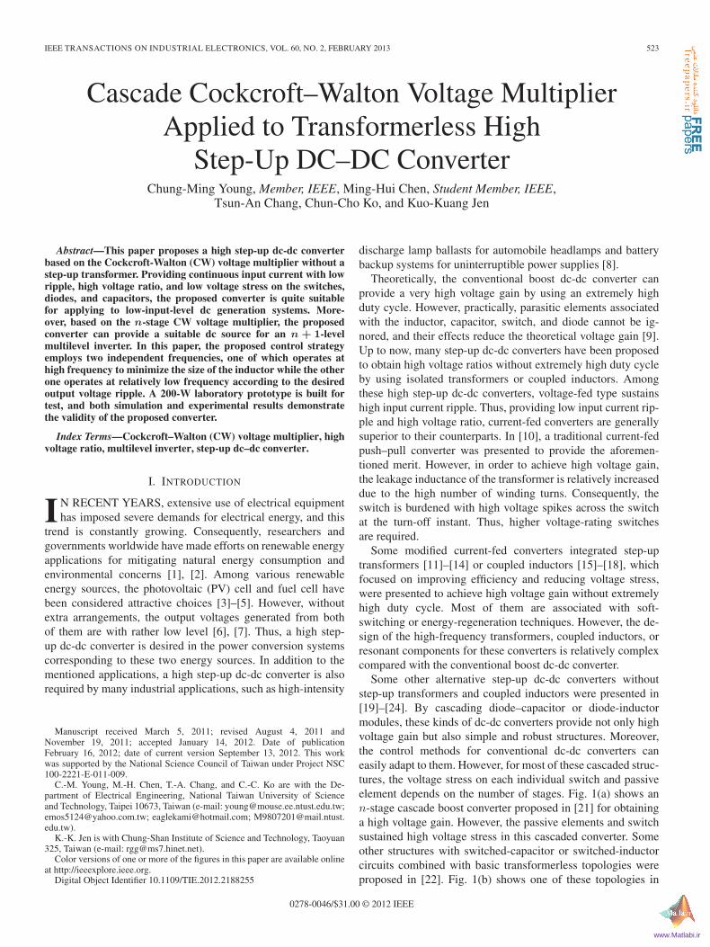
Some other alternative step-up dc-dc converters withoutstep-up transformers and coupled inductors were presented in[19]–[24]. By cascading diode–capacitor or diode-inductormodules, these kinds of dc-dc converters provide not only highvoltage gain but also simple and robust structures. Moreover,the control methods for conventional dc-dc converters caneasily adapt to them. However, for most of these cascaded struc-tures, the voltage stress on each individual switch and passiveelement depends on the number of stages. Fig. 1(a) shows ann-stage cascade boost converter proposed in [21] for obtaininga high voltage gain. However, the passive elements and switchsustained high voltage stress in this cascaded converter. Someother structures with switched-capacitor or switched-inductorcircuits combined with basic transformerless topologies wereproposed in [22]. Fig. 1(b) shows one of these topologies in
0278-0046/$31.00 © 2012 IEEE
www.Matlabi.ir
524 IEEE TRANSACTIONS ON INDUSTRIAL ELECTRONICS, VOL. 60, NO. 2, FEBRUARY 2013
Fig. 1. Some cascaded dc-dc converters. (a) n cascade boost converter [21].(b) Diode-capacitor n-stage step-up multiplier converter [23]. (c) Boost con-verter with cascade voltage multiplier cells [24].
[22], which consists of a conventional boost converter and ann-stage diode–capacitor multiplier detailed in [23]. The mainadvantage of this topology is that higher voltage gain caneasily be obtained by adding the stages of the diode-capacitormultipliers without modifying the main switch circuit. Nev-ertheless, the voltage across each capacitor in each switched-capacitor stage goes higher when a higher stage converter isused. Fig. 1(c) shows another similar topology proposed byPrudente et al. [24] which has advantages similar to that of thetopology in [23]. However, the voltage stress on the capacitorsof higher stage is still rather high. Moreover, in [24], a modifiedtopology, with integrated interleaved multiphase boost con-verter and voltage multiplier, was proposed for high-power ap-plications as well. In this topology, all capacitors in the voltagemultiplier have identical voltage which is equal to Vo/(n + 1).
In the past few decades, high-voltage dc power supplies havebeen widely applied to industries, science, medicine, military,and, particularly, in test equipment, such as X-ray systems, dustfiltering, insulating test, and electrostatic coating [25]–[27].Providing the advantages of high voltage ratio, low voltagestress on the diodes and capacitors, compactness, and costefficiency, the conventional Cockcroft-Walton (CW) voltagemultiplier is very popular among high-voltage dc applications.However, the major drawback is that a high ripple voltageappears at the output when a low-frequency (50 or 60 Hz) utilitysource is used.
In this paper, a high step-up converter based on the CW volt-age multiplier is proposed. Replacing the step-up transformer
Fig. 2. Proposed converter with n-stage CW voltage multiplier.
with the boost-type structure, the proposed converter provideshigher voltage ratio than that of the conventional CW voltagemultiplier. Thus, the proposed converter is suitable for powerconversion applications where high voltage gains are desired.Moreover, the proposed converter operates in continuous con-duction mode (CCM), so the switch stresses, the switchinglosses, and EMI noise can be reduced as well. The proposedconverter deploys four switches, in which Sc1 and Sc2 are usedto generate an alternating source to feed into the CW voltagemultiplier and Sm1 and Sm2 are used to control the inductorenergy to obtain a boost performance. This will increase thecomplexity and cost of the proposed converter because anisolated circuit is necessary to drive the power semiconductorswitches. Nevertheless, the proposed converter still demon-strates some special features: 1) The four switches operateat two independent frequencies, which provide coordinationbetween the output ripple and system efficiency; 2) with samevoltage level, the number of semiconductors in the proposedconverter is competing with some cascaded dc-dc converters[21], [23], [24]; 3) the dc output formed by series capacitors issuitable for powering multilevel inverters; and 4) the proposedconverter can adapt to an ac–dc converter with the same topol-ogy, and that will be a future work of this paper.
In Section II, the mathematical model, circuit operationprinciple, and the ideal static gain will be derived and discussed.The design considerations will be introduced in Section III,and some comparisons between the proposed converter andthe other topologies will be made in this section as well. InSection IV, the control strategy of the proposed converter willbe described. In Section V, a prototype with 200-W rating isbuilt, and both simulation and experimental results are dis-played for verification. Finally, some conclusions are given inSection VI.
II. STEADY-STATE ANALYSIS OF PROPOSED CONVERTER
Fig. 2 shows the proposed converter, which is supplied bya low-level dc source, such as battery, PV module, or fuelcell sources. The proposed converter consists of one boost
YOUNG et al.: CW VOLTAGE MULTIPLIER APPLIED TO TRANSFORMERLESS HIGH STEP-UP DC–DC CONVERTER 525
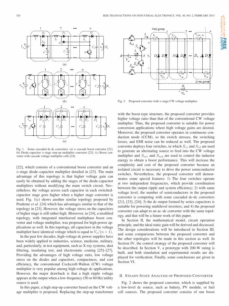
Fig. 3. Equivalent circuit of the proposed converter. (a) Source-side part.(b) Load-side part.
inductor Ls, four switches (Sm1, Sm2, Sc1, and Sc2), andone n-stage CW voltage multiplier. Sm1(Sc1) and Sm2(Sc2)operate in complementary mode, and the operating frequenciesof Sm1 and Sc1 are defined as fsm and fsc, respectively. Forconvenience, fsm is denoted as modulation frequency, and fsc
is denoted as alternating frequency. Theoretically, these two fre-quencies should be as high as possible so that smaller inductorand capacitors can be used in this circuit. In this paper, fsm isset much higher than fsc, and the output voltage is regulatedby controlling the duty cycle of Sm1 and Sm2, while the outputvoltage ripple can be adjusted by fsc. As shown in Fig. 2, thewell-known CW voltage multiplier is constructed by a cascadeof stages with each stage containing two capacitors and twodiodes. In an n-stage CW voltage multiplier, there are N(= 2n)capacitors and N diodes. For convenience, both capacitors anddiodes are divided into odd group and even group according totheir suffixes, as denoted in Fig. 2.
A. Mathematical Model
As shown in Fig. 2, the proposed converter is an integrationof a boost converter with a CW voltage multiplier. For analysis,the equivalent circuit of the proposed converter can be dividedinto source-side and load-side parts as shown in Fig. 3(a) and(b), respectively. For the source-side part, the conducting statesdsc and dsm are defined in Table I, where strategy I doesnot include safe commutation and strategy II includes safecommutation.
According to the conducting states dsc and dsm, the differen-tial equation of the inductor current is given by
diLdt
=1Ls
[Vin − (dsc − dsm) · vγ ] (1)
TABLE ICONDUCTING STATES OF FOUR SWITCHES
Fig. 4. Current-fed three-stage CW voltage multiplier circuit.
where Vin is the input voltage, iL is the input current, and vγ
is the terminal voltage of the CW voltage multiplier. Assumingthat the converter operates in CCM, the current iγ flowing intothe CW voltage multiplier depends on dsm and dsc and can beexpressed as
iγ = (dsc − dsm) · iL (2)
where the current iγ can be deemed a pulse-form currentsource.
In [28], the mathematical model of an n-stage CW voltagemultiplier was discussed and simplified the equivalent circuit,which was convenient for simulation work. Thus, according tothe analysis in [28], the circuit behavior of the load-side part(CW voltage multiplier) will be detailed in the following.
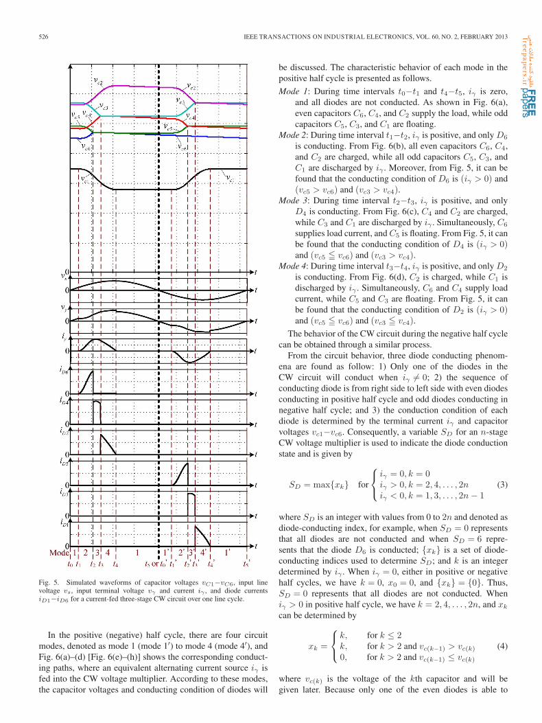
For convenience, a current-fed three-stage CW voltage multi-plier energized by a sinusoidal ac source with line frequency, asshown in Fig. 4, is used to analyze the steady-state behavior ofthe CW circuit through simulation. Obviously, one inductor isconnected between the ac source and the CW voltage multiplierfor smoothing the current iγ . Fig. 5 shows the waveforms ofcapacitor voltages vc1−vc6, line voltage vs, terminal voltage vγ
and current iγ , and diode currents iD1−iD6 over one line cycle,where time interval t0−t5 (t′0−t′5) is the positive (negative) halfcycle. It can be seen from Fig. 5, during positive half cycle,that only one of the even diodes is conducted with the sequenceD6, D4, and D2 and that the even (odd) capacitors are charged(discharged) through the conducting diodes. Similar behavioroccurs during the negative half cycle, while the odd diodes areconducted with the sequence D5, D3, and D1, and the odd(even) capacitors are charged (discharged).
526 IEEE TRANSACTIONS ON INDUSTRIAL ELECTRONICS, VOL. 60, NO. 2, FEBRUARY 2013
Fig. 5. Simulated waveforms of capacitor voltages vC1−vC6, input linevoltage vs, input terminal voltage vγ and current iγ , and diode currentsiD1−iD6 for a current-fed three-stage CW circuit over one line cycle.
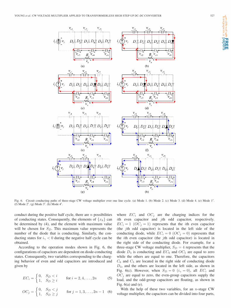
In the positive (negative) half cycle, there are four circuitmodes, denoted as mode 1 (mode 1′) to mode 4 (mode 4′), andFig. 6(a)–(d) [Fig. 6(e)–(h)] shows the corresponding conduct-ing paths, where an equivalent alternating current source iγ isfed into the CW voltage multiplier. According to these modes,the capacitor voltages and conducting condition of diodes will
be discussed. The characteristic behavior of each mode in thepositive half cycle is presented as follows.
Mode 1: During time intervals t0−t1 and t4−t5, iγ is zero,and all diodes are not conducted. As shown in Fig. 6(a),even capacitors C6, C4, and C2 supply the load, while oddcapacitors C5, C3, and C1 are floating.
Mode 2: During time interval t1−t2, iγ is positive, and only D6
is conducting. From Fig. 6(b), all even capacitors C6, C4,and C2 are charged, while all odd capacitors C5, C3, andC1 are discharged by iγ . Moreover, from Fig. 5, it can befound that the conducting condition of D6 is (iγ > 0) and(vc5 > vc6) and (vc3 > vc4).
Mode 3: During time interval t2−t3, iγ is positive, and onlyD4 is conducting. From Fig. 6(c), C4 and C2 are charged,while C3 and C1 are discharged by iγ . Simultaneously, C6
supplies load current, and C5 is floating. From Fig. 5, it canbe found that the conducting condition of D4 is (iγ > 0)and (vc5 � vc6) and (vc3 > vc4).
Mode 4: During time interval t3−t4, iγ is positive, and only D2
is conducting. From Fig. 6(d), C2 is charged, while C1 isdischarged by iγ . Simultaneously, C6 and C4 supply loadcurrent, while C5 and C3 are floating. From Fig. 5, it canbe found that the conducting condition of D2 is (iγ > 0)and (vc5 � vc6) and (vc3 � vc4).
The behavior of the CW circuit during the negative half cyclecan be obtained through a similar process.
From the circuit behavior, three diode conducting phenom-ena are found as follow: 1) Only one of the diodes in theCW circuit will conduct when iγ �= 0; 2) the sequence ofconducting diode is from right side to left side with even diodesconducting in positive half cycle and odd diodes conducting innegative half cycle; and 3) the conduction condition of eachdiode is determined by the terminal current iγ and capacitorvoltages vc1−vc6. Consequently, a variable SD for an n-stageCW voltage multiplier is used to indicate the diode conductionstate and is given by
SD = max{xk} for
⎧⎨⎩
iγ = 0, k = 0iγ > 0, k = 2, 4, . . . , 2niγ < 0, k = 1, 3, . . . , 2n − 1
(3)
where SD is an integer with values from 0 to 2n and denoted asdiode-conducting index, for example, when SD = 0 representsthat all diodes are not conducted and when SD = 6 repre-sents that the diode D6 is conducted; {xk} is a set of diode-conducting indices used to determine SD; and k is an integerdetermined by iγ . When iγ = 0, either in positive or negativehalf cycles, we have k = 0, x0 = 0, and {xk} = {0}. Thus,SD = 0 represents that all diodes are not conducted. Wheniγ > 0 in positive half cycle, we have k = 2, 4, . . . , 2n, and xk
can be determined by
xk =
⎧⎨⎩
k, for k ≤ 2k, for k > 2 and vc(k−1) > vc(k)
0, for k > 2 and vc(k−1) ≤ vc(k)
(4)
where vc(k) is the voltage of the kth capacitor and will begiven later. Because only one of the even diodes is able to
YOUNG et al.: CW VOLTAGE MULTIPLIER APPLIED TO TRANSFORMERLESS HIGH STEP-UP DC–DC CONVERTER 527
Fig. 6. Circuit conducting paths of three-stage CW voltage multiplier over one line cycle. (a) Mode 1. (b) Mode 2. (c) Mode 3. (d) Mode 4. (e) Mode 1′.(f) Mode 2′. (g) Mode 3′. (h) Mode 4′.
conduct during the positive half cycle, there are n possibilitiesof conducting states. Consequently, the elements of {xk} canbe determined by (4), and the element with maximum valuewill be chosen for SD. This maximum value represents thenumber of the diode that is conducting. Similarly, the con-ducting states for iγ < 0 during the negative half cycle can beobtained.
According to the operation modes shown in Fig. 6, theconfigurations of capacitors are dependent on diode-conductingstates. Consequently, two variables corresponding to the charg-ing behavior of even and odd capacitors are introduced andgiven by
ECi ={
0, SD < i1, SD ≥ i
for i = 2, 4, . . . , 2n (5)
OCj ={
0, SD < j1, SD ≥ j
for j = 1, 3, . . . , 2n − 1 (6)
where ECi and OCj are the charging indices for theith even capacitor and jth odd capacitor, respectively.ECi = 1 (OCj = 1) represents that the ith even capacitor(the jth odd capacitor) is located in the left side of theconducting diode, while ECi = 0 (OCj = 0) represents thatthe ith even capacitor (the jth odd capacitor) is located inthe right side of the conducting diode. For example, for athree-stage CW voltage multiplier, SD = 4 represents that thediode D4 is conducting and EC6 and OC5 are equal to zerowhile the others are equal to one. Therefore, the capacitorsC6 and C5 are located in the right side of conducting diodeD4, and the others are located in the left side, as shown inFig. 6(c). However, when SD = 0 (iγ = 0), all ECi andOCj are equal to zero, the even-group capacitors supply theload, and the odd-group capacitors are floating, as shown inFig. 6(a) and (e).
With the help of these two variables, for an n-stage CWvoltage multiplier, the capacitors can be divided into four parts,
528 IEEE TRANSACTIONS ON INDUSTRIAL ELECTRONICS, VOL. 60, NO. 2, FEBRUARY 2013
and the equivalent series voltages of them are given by
vcel =2n∑
i=2,4,...
ECi · vci (7)
vcol =2n−1∑
j=1,3,...
OCj · vcj (8)
vcer =2n∑
i=2,4,...
(1 − ECi) · vci (9)
vcor =2n−1∑
j=1,3,...
(1 − OCj) · vcj (10)
where vcel (vcol) represents the series voltage of even (odd)capacitors that are on the left side of the conducting diode,vcer (vcor) represents the series voltage of even (odd) capacitorsthat are on the right side of the conducting diode, and vci(vcj)is the voltage of the ith even capacitor (the jth odd capacitor).Fig. 3(b) shows the capacitor configuration corresponding tothe conducting diode (SD). From Fig. 3(b), vγ and vo can beexpressed, respectively as
vγ = vcel − vcol (11)
vo = vcel + vcer. (12)
Finally, according to (2), (5), (6), and (12), the currentequations of each even and each odd capacitor are given by
dvci
dt=
1Ci
(ECi · iγ − vo
RL
)for i = 2, 4, . . . , 2n (13)
dvcj
dt=
−1Cj
(OCj · iγ) for j = 1, 3, . . . , 2n − 1 (14)
where Ci is the capacitance of the ith even capacitor and Cj isthe capacitance of the jth odd capacitor. As shown in (13) and(14), the states of ECi (OCj) determine the charge–dischargebehavior of the ith even capacitor (the jth odd capacitor).
From above, one conclusion can be made that, duringone line cycle, each diode conducts equal average currentdue to equality of energy transferring with the sequenceD6−D4−D2−D5−D3−D1, as shown in Fig. 5. Although theproposed converter and the conventional CW voltage multi-plier have different equivalent current iγ , this conclusion isstill available. Finally, the mathematical model of the pro-posed converter described in this section can be used forsimulation.
B. Circuit Operation Principle
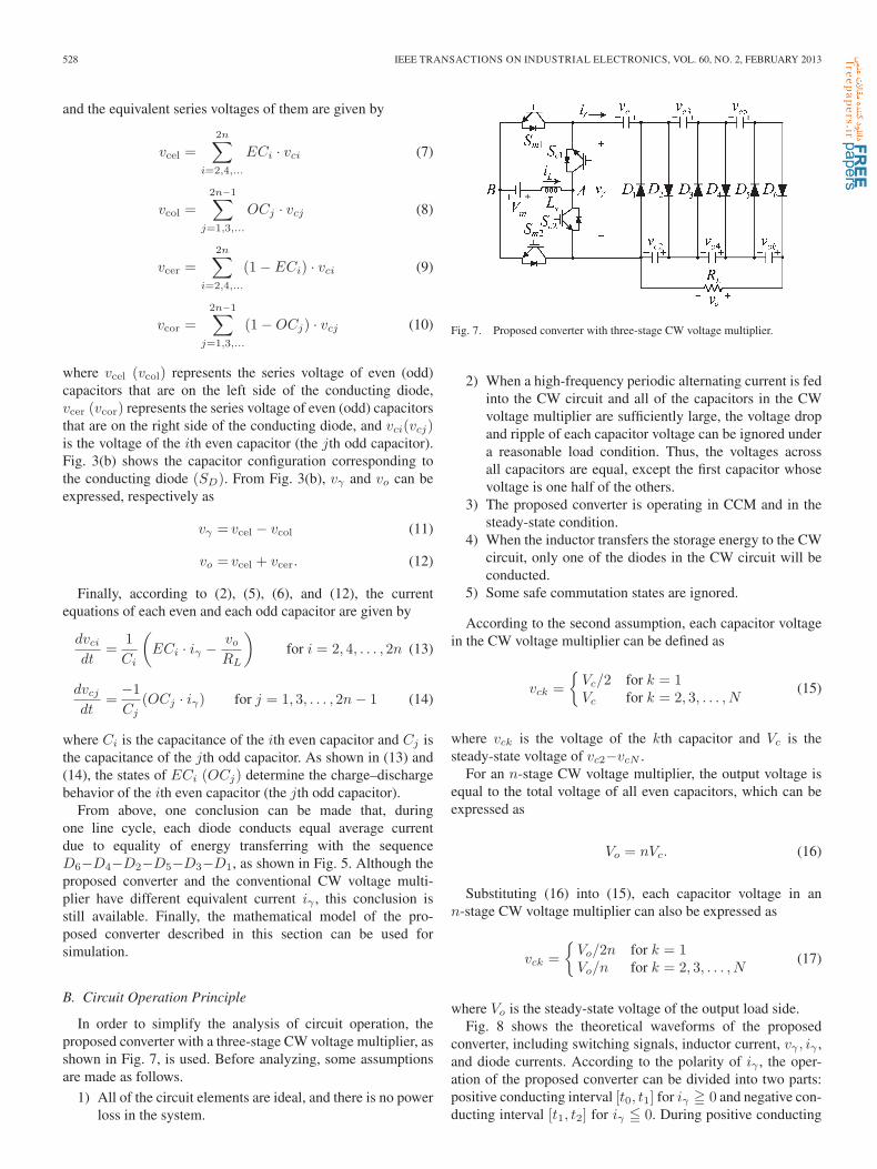
In order to simplify the analysis of circuit operation, theproposed converter with a three-stage CW voltage multiplier, asshown in Fig. 7, is used. Before analyzing, some assumptionsare made as follows.
1) All of the circuit elements are ideal, and there is no powerloss in the system.
Fig. 7. Proposed converter with three-stage CW voltage multiplier.
2) When a high-frequency periodic alternating current is fedinto the CW circuit and all of the capacitors in the CWvoltage multiplier are sufficiently large, the voltage dropand ripple of each capacitor voltage can be ignored undera reasonable load condition. Thus, the voltages acrossall capacitors are equal, except the first capacitor whosevoltage is one half of the others.
3) The proposed converter is operating in CCM and in thesteady-state condition.
4) When the inductor transfers the storage energy to the CWcircuit, only one of the diodes in the CW circuit will beconducted.
5) Some safe commutation states are ignored.
According to the second assumption, each capacitor voltagein the CW voltage multiplier can be defined as
vck ={
Vc/2 for k = 1Vc for k = 2, 3, . . . , N
(15)
where vck is the voltage of the kth capacitor and Vc is thesteady-state voltage of vc2−vcN .
For an n-stage CW voltage multiplier, the output voltage isequal to the total voltage of all even capacitors, which can beexpressed as
Vo = nVc. (16)
Substituting (16) into (15), each capacitor voltage in ann-stage CW voltage multiplier can also be expressed as
vck ={
Vo/2n for k = 1Vo/n for k = 2, 3, . . . , N
(17)
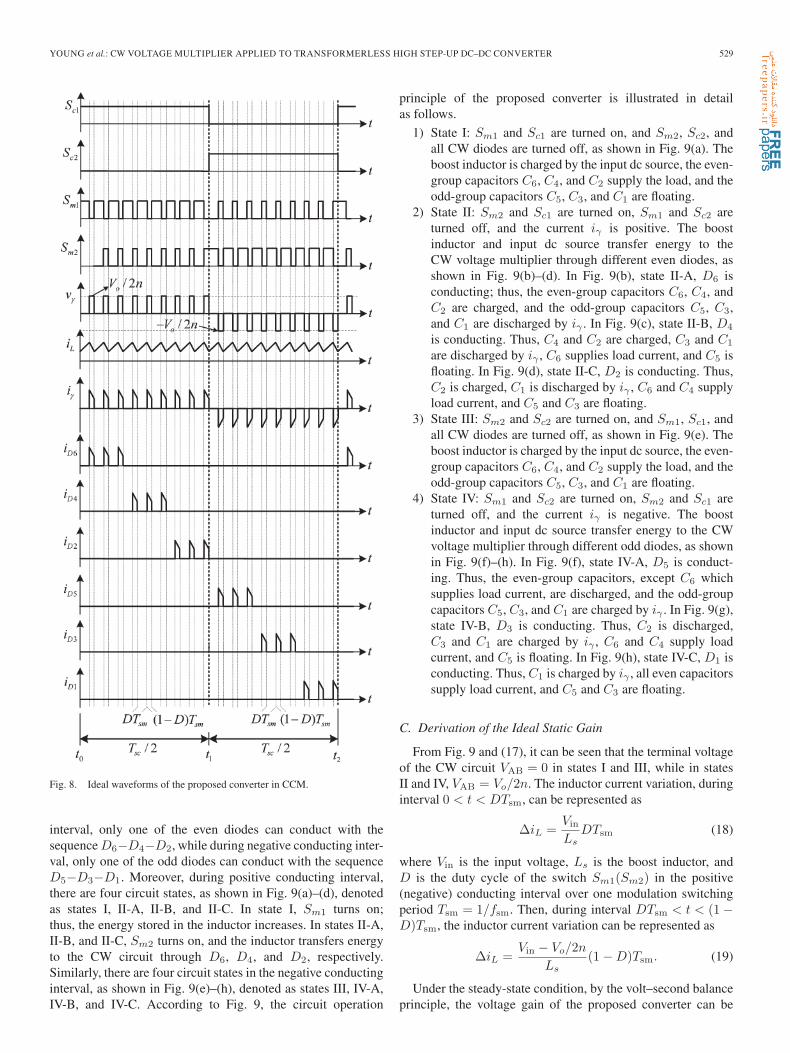
where Vo is the steady-state voltage of the output load side.Fig. 8 shows the theoretical waveforms of the proposed
converter, including switching signals, inductor current, vγ , iγ ,and diode currents. According to the polarity of iγ , the oper-ation of the proposed converter can be divided into two parts:positive conducting interval [t0, t1] for iγ � 0 and negative con-ducting interval [t1, t2] for iγ � 0. During positive conducting
YOUNG et al.: CW VOLTAGE MULTIPLIER APPLIED TO TRANSFORMERLESS HIGH STEP-UP DC–DC CONVERTER 529
Fig. 8. Ideal waveforms of the proposed converter in CCM.
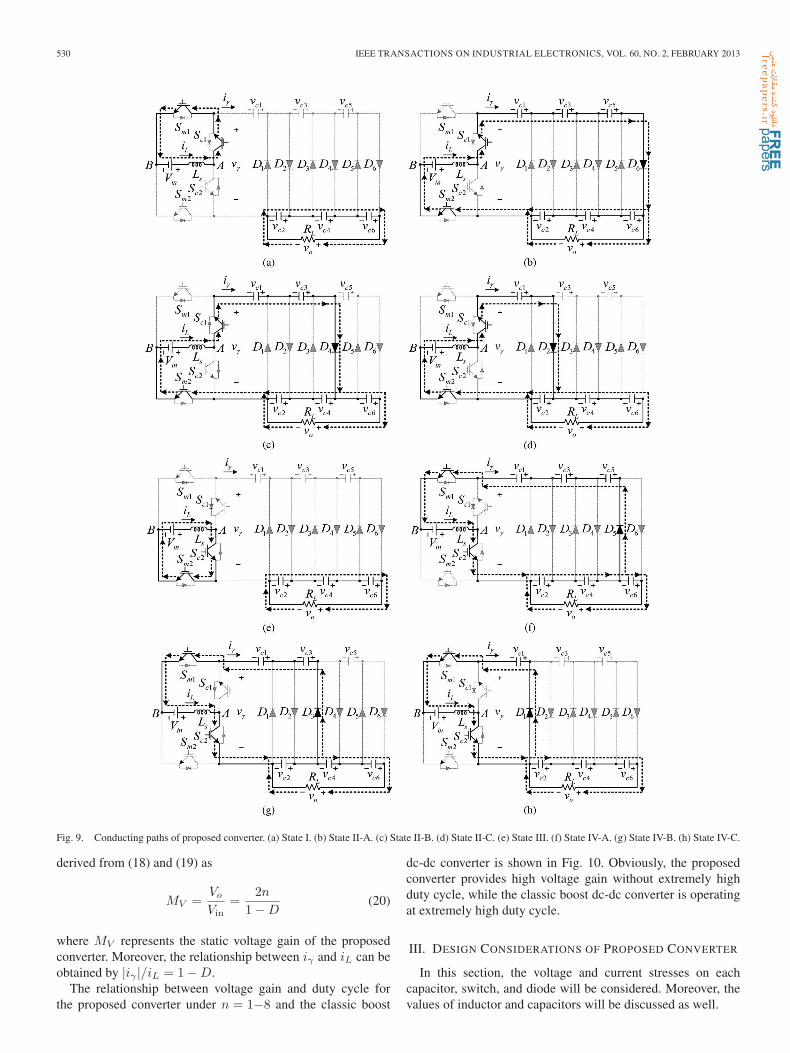
interval, only one of the even diodes can conduct with thesequence D6−D4−D2, while during negative conducting inter-val, only one of the odd diodes can conduct with the sequenceD5−D3−D1. Moreover, during positive conducting interval,there are four circuit states, as shown in Fig. 9(a)–(d), denotedas states I, II-A, II-B, and II-C. In state I, Sm1 turns on;thus, the energy stored in the inductor increases. In states II-A,II-B, and II-C, Sm2 turns on, and the inductor transfers energyto the CW circuit through D6, D4, and D2, respectively.Similarly, there are four circuit states in the negative conductinginterval, as shown in Fig. 9(e)–(h), denoted as states III, IV-A,IV-B, and IV-C. According to Fig. 9, the circuit operation
principle of the proposed converter is illustrated in detailas follows.
1) State I: Sm1 and Sc1 are turned on, and Sm2, Sc2, andall CW diodes are turned off, as shown in Fig. 9(a). Theboost inductor is charged by the input dc source, the even-group capacitors C6, C4, and C2 supply the load, and theodd-group capacitors C5, C3, and C1 are floating.
2) State II: Sm2 and Sc1 are turned on, Sm1 and Sc2 areturned off, and the current iγ is positive. The boostinductor and input dc source transfer energy to theCW voltage multiplier through different even diodes, asshown in Fig. 9(b)–(d). In Fig. 9(b), state II-A, D6 isconducting; thus, the even-group capacitors C6, C4, andC2 are charged, and the odd-group capacitors C5, C3,and C1 are discharged by iγ . In Fig. 9(c), state II-B, D4
is conducting. Thus, C4 and C2 are charged, C3 and C1
are discharged by iγ , C6 supplies load current, and C5 isfloating. In Fig. 9(d), state II-C, D2 is conducting. Thus,C2 is charged, C1 is discharged by iγ , C6 and C4 supplyload current, and C5 and C3 are floating.
3) State III: Sm2 and Sc2 are turned on, and Sm1, Sc1, andall CW diodes are turned off, as shown in Fig. 9(e). Theboost inductor is charged by the input dc source, the even-group capacitors C6, C4, and C2 supply the load, and theodd-group capacitors C5, C3, and C1 are floating.
4) State IV: Sm1 and Sc2 are turned on, Sm2 and Sc1 areturned off, and the current iγ is negative. The boostinductor and input dc source transfer energy to the CWvoltage multiplier through different odd diodes, as shownin Fig. 9(f)–(h). In Fig. 9(f), state IV-A, D5 is conduct-ing. Thus, the even-group capacitors, except C6 whichsupplies load current, are discharged, and the odd-groupcapacitors C5, C3, and C1 are charged by iγ . In Fig. 9(g),state IV-B, D3 is conducting. Thus, C2 is discharged,C3 and C1 are charged by iγ , C6 and C4 supply loadcurrent, and C5 is floating. In Fig. 9(h), state IV-C, D1 isconducting. Thus, C1 is charged by iγ , all even capacitorssupply load current, and C5 and C3 are floating.
C. Derivation of the Ideal Static Gain
From Fig. 9 and (17), it can be seen that the terminal voltageof the CW circuit VAB = 0 in states I and III, while in statesII and IV, VAB = Vo/2n. The inductor current variation, duringinterval 0 < t < DTsm, can be represented as
ΔiL =Vin
LsDTsm (18)
where Vin is the input voltage, Ls is the boost inductor, andD is the duty cycle of the switch Sm1(Sm2) in the positive(negative) conducting interval over one modulation switchingperiod Tsm = 1/fsm. Then, during interval DTsm < t < (1 −D)Tsm, the inductor current variation can be represented as
ΔiL =Vin − Vo/2n
Ls(1 − D)Tsm. (19)
Under the steady-state condition, by the volt–second balanceprinciple, the voltage gain of the proposed converter can be
530 IEEE TRANSACTIONS ON INDUSTRIAL ELECTRONICS, VOL. 60, NO. 2, FEBRUARY 2013
Fig. 9. Conducting paths of proposed converter. (a) State I. (b) State II-A. (c) State II-B. (d) State II-C. (e) State III. (f) State IV-A. (g) State IV-B. (h) State IV-C.
derived from (18) and (19) as
MV =Vo
Vin=
2n
1 − D(20)
where MV represents the static voltage gain of the proposedconverter. Moreover, the relationship between iγ and iL can beobtained by |iγ |/iL = 1 − D.
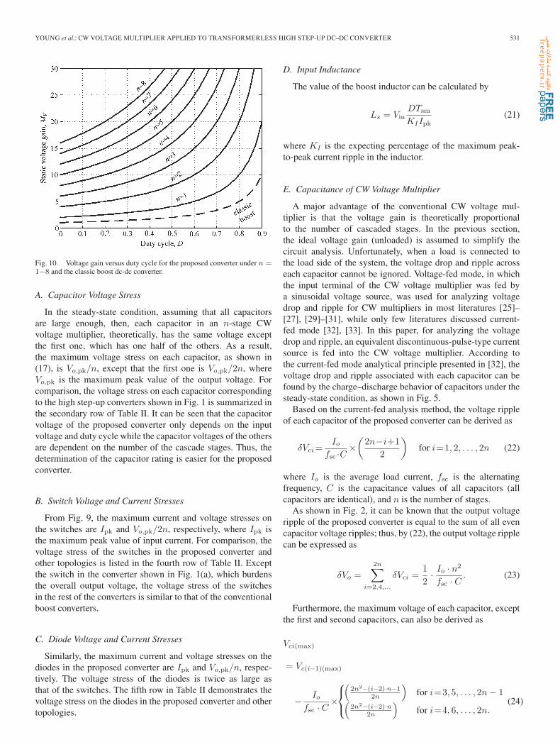
The relationship between voltage gain and duty cycle forthe proposed converter under n = 1−8 and the classic boost
dc-dc converter is shown in Fig. 10. Obviously, the proposedconverter provides high voltage gain without extremely highduty cycle, while the classic boost dc-dc converter is operatingat extremely high duty cycle.
III. DESIGN CONSIDERATIONS OF PROPOSED CONVERTER
In this section, the voltage and current stresses on eachcapacitor, switch, and diode will be considered. Moreover, thevalues of inductor and capacitors will be discussed as well.
YOUNG et al.: CW VOLTAGE MULTIPLIER APPLIED TO TRANSFORMERLESS HIGH STEP-UP DC–DC CONVERTER 531
Fig. 10. Voltage gain versus duty cycle for the proposed converter under n =1−8 and the classic boost dc-dc converter.
A. Capacitor Voltage Stress
In the steady-state condition, assuming that all capacitorsare large enough, then, each capacitor in an n-stage CWvoltage multiplier, theoretically, has the same voltage exceptthe first one, which has one half of the others. As a result,the maximum voltage stress on each capacitor, as shown in(17), is Vo,pk/n, except that the first one is Vo,pk/2n, whereVo,pk is the maximum peak value of the output voltage. Forcomparison, the voltage stress on each capacitor correspondingto the high step-up converters shown in Fig. 1 is summarized inthe secondary row of Table II. It can be seen that the capacitorvoltage of the proposed converter only depends on the inputvoltage and duty cycle while the capacitor voltages of the othersare dependent on the number of the cascade stages. Thus, thedetermination of the capacitor rating is easier for the proposedconverter.
B. Switch Voltage and Current Stresses
From Fig. 9, the maximum current and voltage stresses onthe switches are Ipk and Vo,pk/2n, respectively, where Ipk isthe maximum peak value of input current. For comparison, thevoltage stress of the switches in the proposed converter andother topologies is listed in the fourth row of Table II. Exceptthe switch in the converter shown in Fig. 1(a), which burdensthe overall output voltage, the voltage stress of the switchesin the rest of the converters is similar to that of the conventionalboost converters.
C. Diode Voltage and Current Stresses
Similarly, the maximum current and voltage stresses on thediodes in the proposed converter are Ipk and Vo,pk/n, respec-tively. The voltage stress of the diodes is twice as large asthat of the switches. The fifth row in Table II demonstrates thevoltage stress on the diodes in the proposed converter and othertopologies.
D. Input Inductance
The value of the boost inductor can be calculated by
Ls = VinDTsm
KIIpk(21)
where KI is the expecting percentage of the maximum peak-to-peak current ripple in the inductor.
E. Capacitance of CW Voltage Multiplier
A major advantage of the conventional CW voltage mul-tiplier is that the voltage gain is theoretically proportionalto the number of cascaded stages. In the previous section,the ideal voltage gain (unloaded) is assumed to simplify thecircuit analysis. Unfortunately, when a load is connected tothe load side of the system, the voltage drop and ripple acrosseach capacitor cannot be ignored. Voltage-fed mode, in whichthe input terminal of the CW voltage multiplier was fed bya sinusoidal voltage source, was used for analyzing voltagedrop and ripple for CW multipliers in most literatures [25]–[27], [29]–[31], while only few literatures discussed current-fed mode [32], [33]. In this paper, for analyzing the voltagedrop and ripple, an equivalent discontinuous-pulse-type currentsource is fed into the CW voltage multiplier. According tothe current-fed mode analytical principle presented in [32], thevoltage drop and ripple associated with each capacitor can befound by the charge–discharge behavior of capacitors under thesteady-state condition, as shown in Fig. 5.
Based on the current-fed analysis method, the voltage rippleof each capacitor of the proposed converter can be derived as
δVci =Io
fsc ·C×
(2n−i+1
2
)for i=1, 2, . . . , 2n (22)
where Io is the average load current, fsc is the alternatingfrequency, C is the capacitance values of all capacitors (allcapacitors are identical), and n is the number of stages.
As shown in Fig. 2, it can be known that the output voltageripple of the proposed converter is equal to the sum of all evencapacitor voltage ripples; thus, by (22), the output voltage ripplecan be expressed as
δVo =2n∑
i=2,4,...
δVci =12· Io · n2
fsc · C. (23)
Furthermore, the maximum voltage of each capacitor, exceptthe first and second capacitors, can also be derived as
Vci(max)
= Vc(i−1)(max)
− Io
fsc · C×
⎧⎨⎩
(2n2−(i−2)·n−1
2n
)for i=3, 5, . . . , 2n − 1(
2n2−(i−2)·n2n
)for i=4, 6, . . . , 2n.
(24)
532 IEEE TRANSACTIONS ON INDUSTRIAL ELECTRONICS, VOL. 60, NO. 2, FEBRUARY 2013
TABLE IICOMPARISON OF TOPOLOGIES
From (24), it can be found that the maximum voltage ofthe ith capacitor (i = 3, . . . , 2n) is dependent on the maximumvoltage of the second capacitor with a voltage drop; thus, (24)can be represented as
Vci(max)
= Vc2(max)
− Io
fsc · C×
⎧⎨⎩
�(i−1)/2�∑k=1
2n2−(2k−1)·n−12n
+�(i−2)/2�∑
h=1
2n2−(2h)·n2n
⎫⎬⎭
for i = 3, 4, . . . , 2n (25)
where �X� is the largest integer and not greater than X .Before applying (25), the maximum voltage of the second
capacitor has to be obtained first. For a CW voltage multiplier,the average output voltage is equal to the sum of averagevoltages of all even capacitors and can be expressed as
Vo =2n∑
i=2,4,...
Vci =2n∑
i=2,4,...
(Vci(max) − δVci/2
). (26)
Assuming that the average output voltage Vo is regulatedthrough a closed-loop controller and substituting (22) and (25)into (26), the maximum voltage of the second capacitor can beestimated as
Vc2(max)
=1n
{Vo+
Io
fsc · C
×
⎡⎣ 2n∑
i=2,4,...
2n−i+14
+2n∑
i=4,6,...
(i−2)/2∑k=1
4n2−(4k−1)·n−12n
⎤⎦
⎫⎬⎭ . (27)
To simplify the calculation of Vc2(max), (27) can be ex-pressed as
Vc2(max) =Vo
n+
Io
fsc · C×
(23n2 − 1
2n − 1
6+
14n
). (28)
From (22) and (25), it can be seen that the higher numbercapacitor has smaller voltage ripple and larger voltage drop.Consequently, the second capacitor has both the highest voltageand ripple, which are dependent on Io, fsc, C, and n. Amongthem, the number of stages is most influential. For the proposedconverter, the voltage drop affected by the number of stages ismore obvious than the voltage ripple; the result is similar tothat of the conventional CW voltage multiplier investigated in[25]–[27] and [29]–[31].
Theoretically, each capacitor voltage has identical voltageexcept the first one. However, the voltages of capacitors are notequal to the theoretical value (Vo/n) in practical applications.For design consideration, the voltage difference among allcapacitors should be as small as possible. Thus, higher fsc
and C are selected to achieve this, unless they are beyondpractical limitations or other considerations. With a specifiedVc2(max), (28) can be used to determine the capacitance valueof capacitors in the CW voltage multiplier.
F. Number of Major Components
Referring back to Figs. 1 and 2, it can be seen that thenumbers of diodes and capacitors increase when the numberof the stages goes higher. These two devices, the input inductorand the controllable switch, are the major components of thesekinds of cascaded converters. From this point of view, thenumber of major components is another merit of the proposedconverter. For convenience, the duty cycle is all set to 0.8 forall competitors. Fig. 11 shows the number of major compo-nents versus voltage gain for the proposed converter and thetopologies of Fig. 1(b) and (c). Obviously, the number of majorcomponents of converters shown in Fig. 1(b) and (c) is lesser
YOUNG et al.: CW VOLTAGE MULTIPLIER APPLIED TO TRANSFORMERLESS HIGH STEP-UP DC–DC CONVERTER 533
Fig. 11. Element number versus voltage gain at duty cycle D = 0.8 for theproposed converter and other converters.
than that of the proposed converter when the voltage gain isequal to ten. However, when a higher voltage gain is desired,e.g., Mv = 20, the proposed converter only needs n = 2, andthe total number of major components is 13. With the samevoltage gain, the converter in Fig. 1(c) needs 16 components.Then, for a 19 voltage gain, the converter in Fig. 1(b) needs 16components as well. Moreover, from Fig. 11, it can be seen thatthe difference of the number of major components between theproposed converter and the other converters increases when ahigher voltage gain is desired.
IV. CONTROL STRATEGY OF PROPOSED CONVERTER
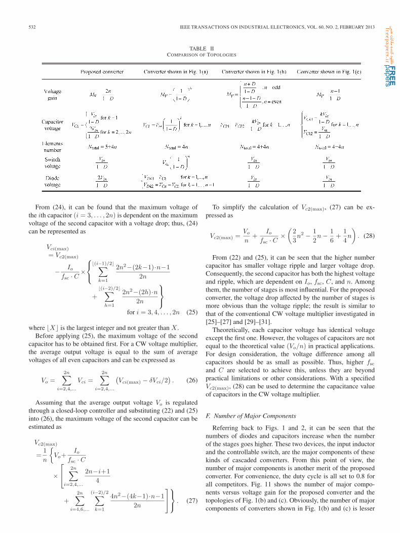
Due to the circuit operation, the proposed converter is sim-ilar to the conventional boost dc-dc converter, except that theproposed converter provides alternating current iγ to the CWvoltage multiplier. Thus, some commercial control ICs for con-ventional boost converters can adopt to the proposed converterwith an extra auxiliary circuit which modifies the original PWMsignal to signals with suitable timing and frequency for the fourswitches.
Taking a close look at the circuit states in Fig. 9, it can befound that Sc1 and Sc2 (Sm1 and Sm2) swap the conductionstates at the changing instant between each state. If the com-mutation fails, the discontinuous inductor current will causevoltage spike and damage the switching elements. However,the switching strategy, as shown in Fig. 8, for the four switchesof the proposed converter is not including safe commutationtechnique. Therefore, another switching strategy including safecommutation technique under the same output function, asshown in Fig. 12, is used in the control strategy of the proposedconverter to avoid open circuit of the inductor. The switchingpatterns of Sc1 and Sc2 place a short overlap time, whileSm2(Sm1) maintains a trigger high level when Sc1(Sc2) isturned on; in this way, it provides a safe commutation to theoperation of the proposed converter.
In this paper, an average-current mode control will be usedto design the PWM modulator in order to achieve the proposedconverter in CCM. For facilitating design, this paper deploys
Fig. 12. Timing diagram of switching patterns for the proposed converterincluding safe commutation states.
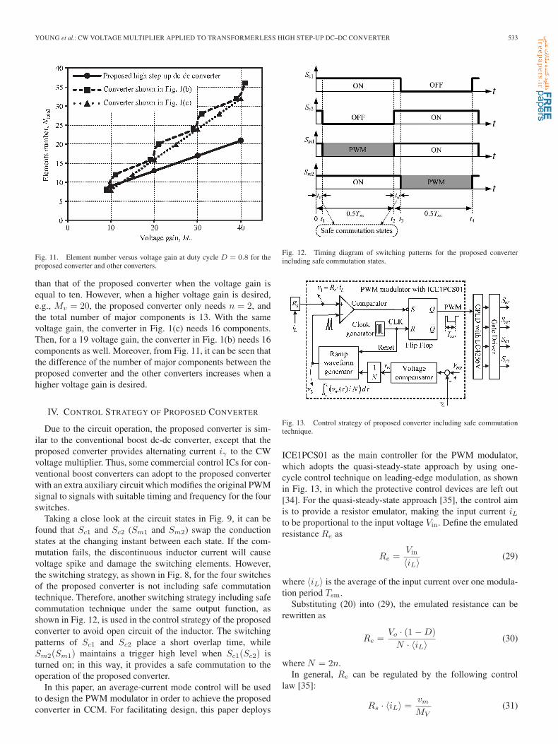
Fig. 13. Control strategy of proposed converter including safe commutationtechnique.
ICE1PCS01 as the main controller for the PWM modulator,which adopts the quasi-steady-state approach by using one-cycle control technique on leading-edge modulation, as shownin Fig. 13, in which the protective control devices are left out[34]. For the quasi-steady-state approach [35], the control aimis to provide a resistor emulator, making the input current iLto be proportional to the input voltage Vin. Define the emulatedresistance Re as
Re =Vin
〈iL〉(29)
where 〈iL〉 is the average of the input current over one modula-tion period Tsm.
Substituting (20) into (29), the emulated resistance can berewritten as
Re =Vo · (1 − D)
N · 〈iL〉(30)
where N = 2n.In general, Re can be regulated by the following control
law [35]:
Rs · 〈iL〉 =vm
MV(31)
534 IEEE TRANSACTIONS ON INDUSTRIAL ELECTRONICS, VOL. 60, NO. 2, FEBRUARY 2013
TABLE IIISYSTEM SPECIFICATIONS OF THE PROTOTYPE
where Rs is the equivalent current-sensing resistance and vm
is the modulation voltage, which is determined by the errorcommand between the reference value Vref and actual valuevo, as shown in Fig. 13. As shown in Fig. 13, the voltagecompensator is used to regulate the output voltage vo throughvm to deliver suitable power to the load. Substituting (20)into (31)
Rs · 〈iL〉 =vm · (1 − D)
N. (32)
Then, according to (30) and (32), Re can be represented as
Re =Rs · Vo
vm. (33)
It can be seen from (33) that if the modulation voltage vm iscontrolled to be a constant, the emulated resistance Re will be aconstant. Consequently, the input current will be proportionalto the input voltage as shown in (29). In other words, theproposed converter operating in CCM can be achieved. Theimplementation of this performance has to regulate the dutycycle D of the PWM modulator to satisfy the control law asshown in (32). Using one-cycle control technology on leading-edge modulation, the PWM modulator, as shown in Fig. 13,is constructed by a constant time clock generator, a voltagecomparator, an SR flip-flop, and a ramp waveform generatorwith reset. For practical applications, the average inductorcurrent can be approximately equal to the instant inductorwhen the current ripple in the inductor is negligible during onemodulation period [35]. Therefore, in this paper, the functionsv1 and v2, as shown in Fig. 13, are set to implement the controllaw (32).
The PWM signal including boost function in CCM is ob-tained from the operation of PWM modulator. The PWMsignal is fed into a preprogrammed complex programmablelogic device, CPLD LC4256V, as shown in Fig. 13. A timerestablished in the CPLD is used to set the alternating periodTsc or alternating frequency fsc. In addition, a logical circuitprogrammed in the same CPLD modifies the PWM signal fromICE1PCS01 and then sends the modified signals to trig the fourswitches. An overlap with interval td for safe commutation isimplemented in the CPLD as well.
V. SIMULATION AND EXPERIMENTAL RESULTS
A prototype with 200-W rating was built to verify the validityof the proposed converter. The system specifications and com-ponents of the prototype are summarized in Tables III and IV,respectively. Moreover, Matlab/Simulink is applied to simulate
TABLE IVCOMPONENT LIST FOR THE PROTOTYPE
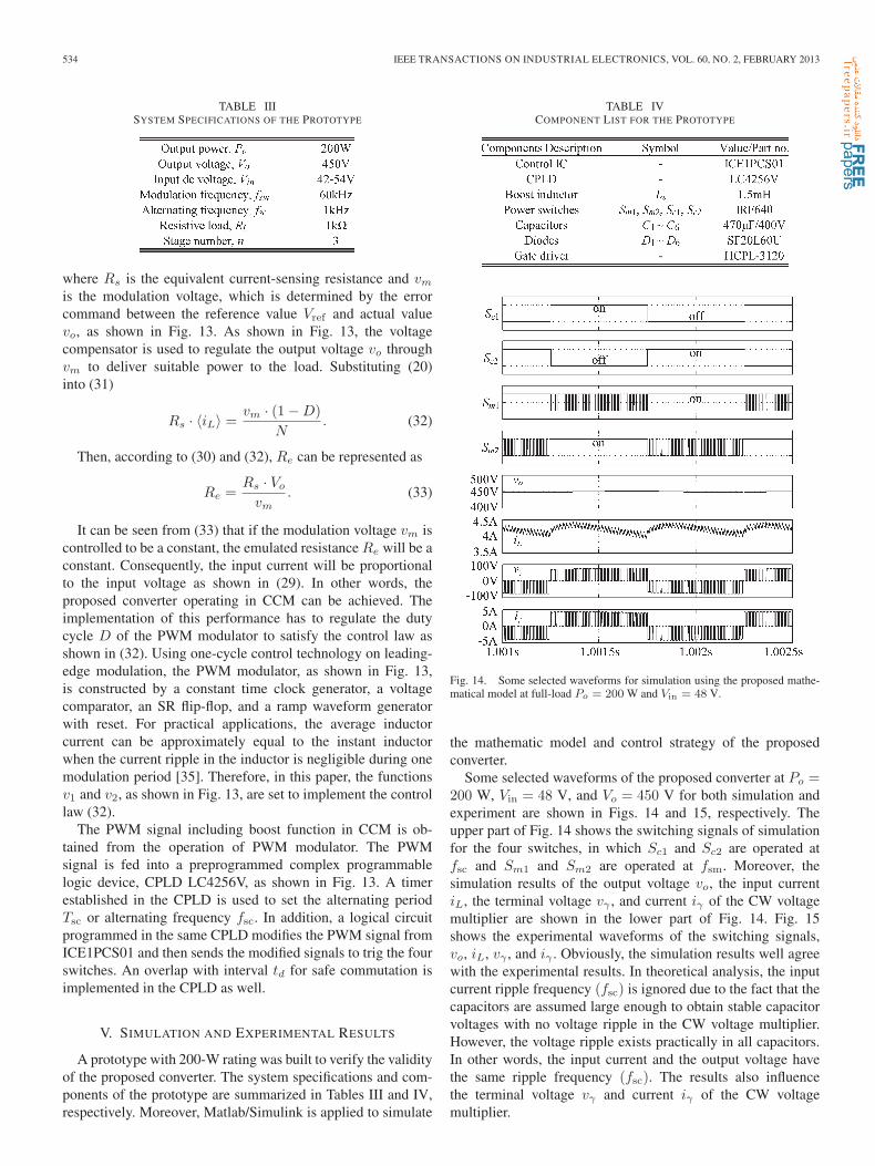
Fig. 14. Some selected waveforms for simulation using the proposed mathe-matical model at full-load Po = 200 W and Vin = 48 V.
the mathematic model and control strategy of the proposedconverter.
Some selected waveforms of the proposed converter at Po =200 W, Vin = 48 V, and Vo = 450 V for both simulation andexperiment are shown in Figs. 14 and 15, respectively. Theupper part of Fig. 14 shows the switching signals of simulationfor the four switches, in which Sc1 and Sc2 are operated atfsc and Sm1 and Sm2 are operated at fsm. Moreover, thesimulation results of the output voltage vo, the input currentiL, the terminal voltage vγ , and current iγ of the CW voltagemultiplier are shown in the lower part of Fig. 14. Fig. 15shows the experimental waveforms of the switching signals,vo, iL, vγ , and iγ . Obviously, the simulation results well agreewith the experimental results. In theoretical analysis, the inputcurrent ripple frequency (fsc) is ignored due to the fact that thecapacitors are assumed large enough to obtain stable capacitorvoltages with no voltage ripple in the CW voltage multiplier.However, the voltage ripple exists practically in all capacitors.In other words, the input current and the output voltage havethe same ripple frequency (fsc). The results also influencethe terminal voltage vγ and current iγ of the CW voltagemultiplier.
YOUNG et al.: CW VOLTAGE MULTIPLIER APPLIED TO TRANSFORMERLESS HIGH STEP-UP DC–DC CONVERTER 535
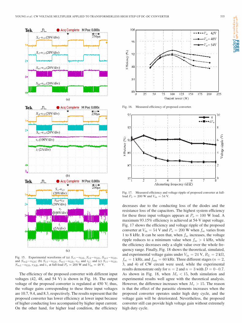
Fig. 15. Experimental waveforms of (a) Sc1−vGS, Sc2−vGS, Sm1−vGS,and Sm2−vGS; (b) Sc1−vGS, Sm1−vGS, vo, and iL; and (c) Sc1−vGS,Sm1−vGS, vAB, and iγ at full-load Po = 200 W and Vin = 48 V.
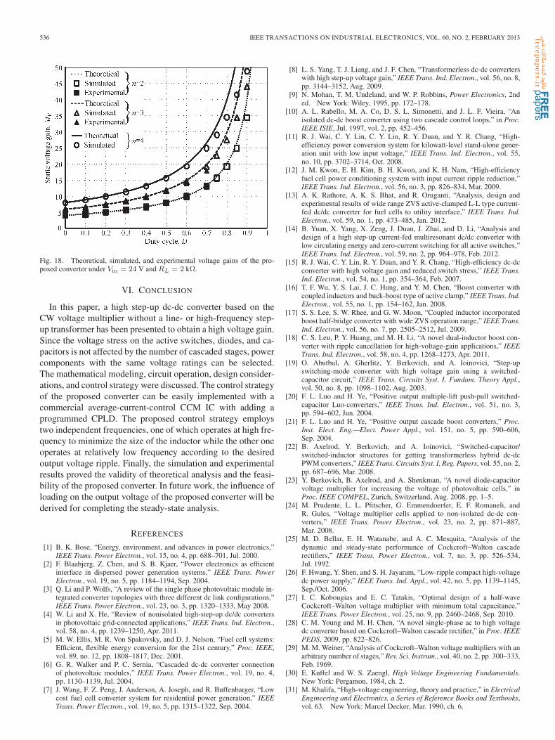
The efficiency of the proposed converter with different inputvoltages (42, 48, and 54 V) is shown in Fig. 16. The outputvoltage of the proposed converter is regulated at 450 V; thus,the voltage gains corresponding to these three input voltagesare 10.7, 9.4, and 8.3, respectively. The results represent that theproposed converter has lower efficiency at lower input becauseof higher conducting loss accompanied by higher input current.On the other hand, for higher load condition, the efficiency
Fig. 16. Measured efficiency of proposed converter.
Fig. 17. Measured efficiency and voltage ripple of proposed converter at full-load Po = 200 W and Vin = 54 V.
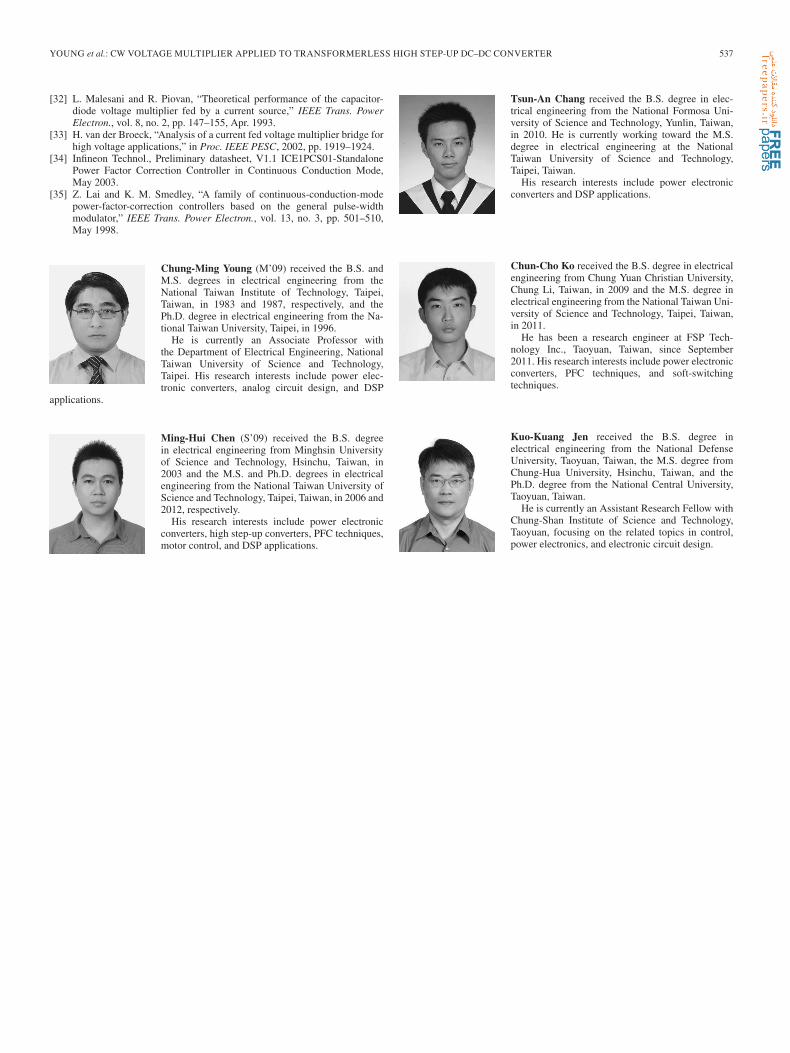
decreases due to the conducting loss of the diodes and theresistance loss of the capacitors. The highest system efficiencyfor these three input voltages appears at Po = 100 W load. Amaximum 93.15% efficiency is achieved at 54-V input voltage.Fig. 17 shows the efficiency and voltage ripple of the proposedconverter at Vin = 54 V and Po = 200 W when fsc varies from1 to 8 kHz. It can be seen that, when fsc increases, the voltageripple reduces to a minimum value when fsc > 4 kHz, whilethe efficiency decreases only a slight value over the whole fre-quency range. Finally, Fig. 18 shows the theoretical, simulated,and experimental voltage gains under Vin = 24 V, RL = 2 kΩ,fsc = 1 kHz, and fsm = 60 kHz. Three different stages (n = 2,3, and 4) of CW circuit were used, while the experimentalresults demonstrate only for n = 2 and n = 3 with D = 0−0.7.As shown in Fig. 18, when Mv < 15, both simulation andexperimental results well agree with the theoretical analysis.However, the difference increases when Mv > 15. The reasonis that the effect of the parasitic elements increases when theproposed converter operates under high duty cycle, and thevoltage gain will be deteriorated. Nevertheless, the proposedconverter still can provide high voltage gain without extremelyhigh duty cycle.
536 IEEE TRANSACTIONS ON INDUSTRIAL ELECTRONICS, VOL. 60, NO. 2, FEBRUARY 2013
Fig. 18. Theoretical, simulated, and experimental voltage gains of the pro-posed converter under Vin = 24 V and RL = 2 kΩ.
VI. CONCLUSION
In this paper, a high step-up dc-dc converter based on theCW voltage multiplier without a line- or high-frequency step-up transformer has been presented to obtain a high voltage gain.Since the voltage stress on the active switches, diodes, and ca-pacitors is not affected by the number of cascaded stages, powercomponents with the same voltage ratings can be selected.The mathematical modeling, circuit operation, design consider-ations, and control strategy were discussed. The control strategyof the proposed converter can be easily implemented with acommercial average-current-control CCM IC with adding aprogrammed CPLD. The proposed control strategy employstwo independent frequencies, one of which operates at high fre-quency to minimize the size of the inductor while the other oneoperates at relatively low frequency according to the desiredoutput voltage ripple. Finally, the simulation and experimentalresults proved the validity of theoretical analysis and the feasi-bility of the proposed converter. In future work, the influence ofloading on the output voltage of the proposed converter will bederived for completing the steady-state analysis.
REFERENCES
[1] B. K. Bose, “Energy, environment, and advances in power electronics,”IEEE Trans. Power Electron., vol. 15, no. 4, pp. 688–701, Jul. 2000.
[2] F. Blaabjerg, Z. Chen, and S. B. Kjaer, “Power electronics as efficientinterface in dispersed power generation systems,” IEEE Trans. PowerElectron., vol. 19, no. 5, pp. 1184–1194, Sep. 2004.
[3] Q. Li and P. Wolfs, “A review of the single phase photovoltaic module in-tegrated converter topologies with three different dc link configurations,”IEEE Trans. Power Electron., vol. 23, no. 3, pp. 1320–1333, May 2008.
[4] W. Li and X. He, “Review of nonisolated high-step-up dc/dc convertersin photovoltaic grid-connected applications,” IEEE Trans. Ind. Electron.,vol. 58, no. 4, pp. 1239–1250, Apr. 2011.
[5] M. W. Ellis, M. R. Von Spakovsky, and D. J. Nelson, “Fuel cell systems:Efficient, flexible energy conversion for the 21st century,” Proc. IEEE,vol. 89, no. 12, pp. 1808–1817, Dec. 2001.
[6] G. R. Walker and P. C. Sernia, “Cascaded dc-dc converter connectionof photovoltaic modules,” IEEE Trans. Power Electron., vol. 19, no. 4,pp. 1130–1139, Jul. 2004.
[7] J. Wang, F. Z. Peng, J. Anderson, A. Joseph, and R. Buffenbarger, “Lowcost fuel cell converter system for residential power generation,” IEEETrans. Power Electron., vol. 19, no. 5, pp. 1315–1322, Sep. 2004.
[8] L. S. Yang, T. J. Liang, and J. F. Chen, “Transformerless dc-dc converterswith high step-up voltage gain,” IEEE Trans. Ind. Electron., vol. 56, no. 8,pp. 3144–3152, Aug. 2009.
[9] N. Mohan, T. M. Undeland, and W. P. Robbins, Power Electronics, 2nded. New York: Wiley, 1995, pp. 172–178.
[10] A. L. Rabello, M. A. Co, D. S. L. Simonetti, and J. L. F. Vieira, “Anisolated dc-dc boost converter using two cascade control loops,” in Proc.IEEE ISIE, Jul. 1997, vol. 2, pp. 452–456.
[11] R. J. Wai, C. Y. Lin, C. Y. Lin, R. Y. Duan, and Y. R. Chang, “High-efficiency power conversion system for kilowatt-level stand-alone gener-ation unit with low input voltage,” IEEE Trans. Ind. Electron., vol. 55,no. 10, pp. 3702–3714, Oct. 2008.
[12] J. M. Kwon, E. H. Kim, B. H. Kwon, and K. H. Nam, “High-efficiencyfuel cell power conditioning system with input current ripple reduction,”IEEE Trans. Ind. Electron., vol. 56, no. 3, pp. 826–834, Mar. 2009.
[13] A. K. Rathore, A. K. S. Bhat, and R. Oruganti, “Analysis, design andexperimental results of wide range ZVS active-clamped L-L type current-fed dc/dc converter for fuel cells to utility interface,” IEEE Trans. Ind.Electron., vol. 59, no. 1, pp. 473–485, Jan. 2012.
[14] B. Yuan, X. Yang, X. Zeng, J. Duan, J. Zhai, and D. Li, “Analysis anddesign of a high step-up current-fed multiresonant dc/dc converter withlow circulating energy and zero-current switching for all active switches,”IEEE Trans. Ind. Electron., vol. 59, no. 2, pp. 964–978, Feb. 2012.
[15] R. J. Wai, C. Y. Lin, R. Y. Duan, and Y. R. Chang, “High-efficiency dc-dcconverter with high voltage gain and reduced switch stress,” IEEE Trans.Ind. Electron., vol. 54, no. 1, pp. 354–364, Feb. 2007.
[16] T. F. Wu, Y. S. Lai, J. C. Hung, and Y. M. Chen, “Boost converter withcoupled inductors and buck-boost type of active clamp,” IEEE Trans. Ind.Electron., vol. 55, no. 1, pp. 154–162, Jan. 2008.
[17] S. S. Lee, S. W. Rhee, and G. W. Moon, “Coupled inductor incorporatedboost half-bridge converter with wide ZVS operation range,” IEEE Trans.Ind. Electron., vol. 56, no. 7, pp. 2505–2512, Jul. 2009.
[18] C. S. Leu, P. Y. Huang, and M. H. Li, “A novel dual-inductor boost con-verter with ripple cancellation for high-voltage-gain applications,” IEEETrans. Ind. Electron., vol. 58, no. 4, pp. 1268–1273, Apr. 2011.
[19] O. Abutbul, A. Gherlitz, Y. Berkovich, and A. Ioinovici, “Step-upswitching-mode converter with high voltage gain using a switched-capacitor circuit,” IEEE Trans. Circuits Syst. I, Fundam. Theory Appl.,vol. 50, no. 8, pp. 1098–1102, Aug. 2003.
[20] F. L. Luo and H. Ye, “Positive output multiple-lift push-pull switched-capacitor Luo-converters,” IEEE Trans. Ind. Electron., vol. 51, no. 3,pp. 594–602, Jun. 2004.
[21] F. L. Luo and H. Ye, “Positive output cascade boost converters,” Proc.Inst. Elect. Eng.—Elect. Power Appl., vol. 151, no. 5, pp. 590–606,Sep. 2004.
[22] B. Axelrod, Y. Berkovich, and A. Ioinovici, “Switched-capacitor/switched-inductor structures for getting transformerless hybrid dc-dcPWM converters,” IEEE Trans. Circuits Syst. I, Reg. Papers, vol. 55, no. 2,pp. 687–696, Mar. 2008.
[23] Y. Berkovich, B. Axelrod, and A. Shenkman, “A novel diode-capacitorvoltage multiplier for increasing the voltage of photovoltaic cells,” inProc. IEEE COMPEL, Zurich, Switzerland, Aug. 2008, pp. 1–5.
[24] M. Prudente, L. L. Pfitscher, G. Emmendoerfer, E. F. Romaneli, andR. Gules, “Voltage multiplier cells applied to non-isolated dc-dc con-verters,” IEEE Trans. Power Electron., vol. 23, no. 2, pp. 871–887,Mar. 2008.
[25] M. D. Bellar, E. H. Watanabe, and A. C. Mesquita, “Analysis of thedynamic and steady-state performance of Cockcroft–Walton cascaderectifiers,” IEEE Trans. Power Electron., vol. 7, no. 3, pp. 526–534,Jul. 1992.
[26] F. Hwang, Y. Shen, and S. H. Jayaram, “Low-ripple compact high-voltagedc power supply,” IEEE Trans. Ind. Appl., vol. 42, no. 5, pp. 1139–1145,Sep./Oct. 2006.
[27] I. C. Kobougias and E. C. Tatakis, “Optimal design of a half-waveCockcroft–Walton voltage multiplier with minimum total capacitance,”IEEE Trans. Power Electron., vol. 25, no. 9, pp. 2460–2468, Sep. 2010.
[28] C. M. Young and M. H. Chen, “A novel single-phase ac to high voltagedc converter based on Cockcroft–Walton cascade rectifier,” in Proc. IEEEPEDS, 2009, pp. 822–826.
[29] M. M. Weiner, “Analysis of Cockcroft–Walton voltage multipliers with anarbitrary number of stages,” Rev. Sci. Instrum., vol. 40, no. 2, pp. 300–333,Feb. 1969.
[30] E. Kuffel and W. S. Zaengl, High Voltage Engineering Fundamentals.New York: Pergamon, 1984, ch. 2.
[31] M. Khalifa, “High-voltage engineering, theory and practice,” in ElectricalEngineering and Electronics, a Series of Reference Books and Textbooks,vol. 63. New York: Marcel Decker, Mar. 1990, ch. 6.
YOUNG et al.: CW VOLTAGE MULTIPLIER APPLIED TO TRANSFORMERLESS HIGH STEP-UP DC–DC CONVERTER 537
[32] L. Malesani and R. Piovan, “Theoretical performance of the capacitor-diode voltage multiplier fed by a current source,” IEEE Trans. PowerElectron., vol. 8, no. 2, pp. 147–155, Apr. 1993.
[33] H. van der Broeck, “Analysis of a current fed voltage multiplier bridge forhigh voltage applications,” in Proc. IEEE PESC, 2002, pp. 1919–1924.
[34] Infineon Technol., Preliminary datasheet, V1.1 ICE1PCS01-StandalonePower Factor Correction Controller in Continuous Conduction Mode,May 2003.
[35] Z. Lai and K. M. Smedley, “A family of continuous-conduction-modepower-factor-correction controllers based on the general pulse-widthmodulator,” IEEE Trans. Power Electron., vol. 13, no. 3, pp. 501–510,May 1998.
Chung-Ming Young (M’09) received the B.S. andM.S. degrees in electrical engineering from theNational Taiwan Institute of Technology, Taipei,Taiwan, in 1983 and 1987, respectively, and thePh.D. degree in electrical engineering from the Na-tional Taiwan University, Taipei, in 1996.
He is currently an Associate Professor withthe Department of Electrical Engineering, NationalTaiwan University of Science and Technology,Taipei. His research interests include power elec-tronic converters, analog circuit design, and DSP
applications.
Ming-Hui Chen (S’09) received the B.S. degreein electrical engineering from Minghsin Universityof Science and Technology, Hsinchu, Taiwan, in2003 and the M.S. and Ph.D. degrees in electricalengineering from the National Taiwan University ofScience and Technology, Taipei, Taiwan, in 2006 and2012, respectively.
His research interests include power electronicconverters, high step-up converters, PFC techniques,motor control, and DSP applications.
Tsun-An Chang received the B.S. degree in elec-trical engineering from the National Formosa Uni-versity of Science and Technology, Yunlin, Taiwan,in 2010. He is currently working toward the M.S.degree in electrical engineering at the NationalTaiwan University of Science and Technology,Taipei, Taiwan.
His research interests include power electronicconverters and DSP applications.
Chun-Cho Ko received the B.S. degree in electricalengineering from Chung Yuan Christian University,Chung Li, Taiwan, in 2009 and the M.S. degree inelectrical engineering from the National Taiwan Uni-versity of Science and Technology, Taipei, Taiwan,in 2011.
He has been a research engineer at FSP Tech-nology Inc., Taoyuan, Taiwan, since September2011. His research interests include power electronicconverters, PFC techniques, and soft-switchingtechniques.
Kuo-Kuang Jen received the B.S. degree inelectrical engineering from the National DefenseUniversity, Taoyuan, Taiwan, the M.S. degree fromChung-Hua University, Hsinchu, Taiwan, and thePh.D. degree from the National Central University,Taoyuan, Taiwan.
He is currently an Assistant Research Fellow withChung-Shan Institute of Science and Technology,Taoyuan, focusing on the related topics in control,power electronics, and electronic circuit design.


![IEEE TRANSACTIONS ON INDUSTRIAL ELECTRONICS 1 ......A power electronics based Cockcroft-Walton multiplier has been demonstrated in [21]. This is a light and cheap solution for high](https://img.pdfslide.us/doc/110x75/60397f10aa142977ef6bdde4/ieee-transactions-on-industrial-electronics-1-a-power-electronics-based.jpg)