Embed Size (px)
Citation preview

Prof. Dr. Esko I. Kauppinen
NanoMaterials Group (NMG)
Department of Applied Physics
Helsinki University of Technology
(TKK)
Espoo, Finland
FINNISH-JAPANESE WORKSHOP on FUNCTONAL MATERIALS
Säätytalo 26.5.2009, Helsinki, Finland
Carbon NanoBuds (CNB) – Synthesis,
Structure and Thin Film Device
Applications

NanoMaterials
(NanoMat)
GroupDepartment of Applied Physics
and Center for New Materials
Helsinki University of Technology (TKK)
1). Synthesis of carbon nanotubes and nanobuds
2). Synthesis of multicomponent nano- and microparticles for drug
and gene delivery
3). Structural characterization of nanotubes and nanoparticles by
electron microscopy
4). Generation of novel 2-D and 3-d nanotube, nanobud and
polymer/protein structures for transparent electronics and
energy applications
5). MD and DFT
Nanobud
Carbon nanotube http://www.fyslab.hut.fi/nanomat

NanoMaterials Group, Helsinki University of Technology
Dept. of Applied Physics & Center for New Materials
http://www.fyslab.hut.fi/nanomat/
Acknowledgement for Funding
* Academy of Finland
* EU FP6 & FP7
* TEKES FinNano Program
Dr. Albert G. Nasibulin Dr. Hua Jiang Dr. Janne Raula
Dr. David P. Brown
CEO, Canatu Oy
Mrs. Jing Tian
Ms. Marina Zavodchikova
TKK 100th Anniv. Fund
Also: Antti Kaskela, Toma Susi
NEDO

• Personnel
– 1 prof. and 5 post-docs
– 10 graduate and 7 undergraduate students
• Doctoral level expertise
– Carbon nanotubes, nanobuds, metal oxide nanowires
(Albert G. Nasibulin - phys.chem)
– Drug, polymer, peptide and protein chemistry, nanoparticle synthesis and CNT & CNB surface functionalisation (Janne Raula – polymer mat.)
– Transmission electron microscopy of nanomaterials (Hua Jiang - physics)
– Electrochemistry with carbon nanomaterials – FC&SC (Virginia Ruiz – phys. chem)
– Molecular dynamics and DFT (Markus Kaukonen - physics)
• External Funding
– More than 1 000 k€/year
– EU: BNC Tubes – Strep 2007-2010 3 500 k€; NanoTox – SSA
– Academy of Finland (e.g. NanoDuraMEA), TEKES, companies
– CNB-E 2008-2012 MIDE/TKK 100 Years Anniversary Research Program

Acknowledgements for Collaboration –Prof. Yutka Phno, Nagoya U.
Prof. Florian Banhart, U. Strasbourg
Brad Aitchison, Jussi Sarkkinen, Canatu Oy
Dr. Peter V. Pikhitsa and Prof. Mansoo Choi
National CRI Center for Nano Particle Control, Institute of Advanced
Machinery and Design, Seoul National University, Korea
Dr. Abdou Hassanien and Dr. Günther Lientschnig
AIST, Tsukuba, Japan
Dr. Giulio Lolli and Prof. Daniel E. Resasco
Chemical Biological and Materials Engineering, University of Oklahoma,
USA
Dr. Arkady V. Krasheninnikov and Prof. Risto Nieminen
Laboratory of Physics, Helsinki University of Technology, Finland
Prof. David Tománek
Physics and Astronomy Department, Michigan State University, USA

Known forms of Carbon NanomaterialsCarbon Nanotube (SWCNT):
Roll of carbon sheet one atomic layer thick
= Graphene NanoRibbons (GNR)
1 000 000 times thinner than paper
(10,10) armchair tube
METALLIC
(10,5) helical (chiral) tube
SEMICONDUCTING
Rolling in different directions makes different kinds of tubes
By Prof. Shigeo Maruyama, Tokyo Universssity, Japan

CNTN -Materials for Flexible Electronics
Mo
bility
Year
CNTN FET
According to Prof. G. Gruner, UCLA,USA

Properties of Carbon Nanotubes
• Better conductor than copper
• Better transistor material than silicon
• Conduct heat twice as efficiently as diamond
• Field emit 500 times as efficiently as molybdenum
• Thermally stable up to 1500 oC while polymers degrade below 150 oC
• Half as dense as aluminum
• 25 times stronger than steel
• Very inert and difficult to integrate into composite materials and to incorporate into electronics manufacturing

Three allotropic modifications of carbon: diamond, graphite,
and fullerene structures (fullerenes and CNTs).
??
PEAPOD
Graphene
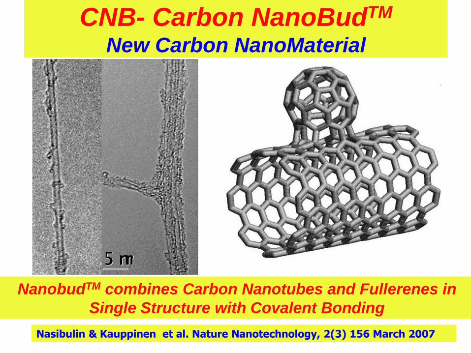
CNB- Carbon NanoBudTM
New Carbon NanoMaterial
NanobudTM combines Carbon Nanotubes and Fullerenes in
Single Structure with Covalent Bonding
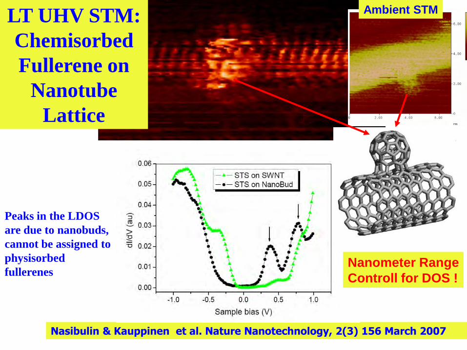
Nasibulin & Kauppinen et al. Nature Nanotechnology, 2(3) 156 March 2007

Content of the Talk
• CNB’s (Carbon NanoBuds = C60+SWCNT) –floating CVD synthesis, structure and properties
• Novel Dry Thin Film Device Manufacturing Method
• Field Electron Emission of CNB vs SWCNT films
• Transparent flexible electrode and TFT
• Preliminary results on nanocarbon PEMFC applications

Mechanism of
CNB Formation
from CO with Fe
Cluster Catalyst
CO
CO
. .
.
.
. .
. .
.
. CO
. CO
CO
Particle saturation by C- REACTIONS: 2CO=C+CO2 AND H2+CO=C+H2O- C RELEASE ON SURFACE- C DISSOLUTION
CO.
. CO
Formation of graphene layer- HEXAGON AND PENTAGON FORMATION
CO.
CNT nucleation- HEPTAGON FORMATION
Steady-state growth of CNT- C INCORPORATION INTO GRAPHENE LAYER - REACTIONS OF CARBON RELEASE AND ETCHING:
FE particle formation - VAPOUR NUCLEATION - CONDENSATION- CLUSTER COAGULATION
H2/N2
. . . .
. . . .
. . . .
. . .
. . . .
. . .
. . . .
. . . . . . . . . . .
Fe(g)
H2
End of CNT growth - CARBON DISPROPRTIONATION IS PROHIBITED (t > 900 °C)
HE
AT
ING
ZO
NE
TE
MP
ER
AT
UR
E
HIG
H
ZO
NE
CO.
CO.
CO.
400 °C
900 °C
CO2 reaction with amorphous carbon:
C+CO2 = 2CO
CO. CO.
CO2
C
- REACTIONS ON REACTOR WALLS: 2CO=C+CO2 H2+CO=C+H2O
- CO2 AND H2O
RELEASE
.
.
CO2
H2O
. . 2CO<=>C+CO2 AND H2+CO<=>C+H2O
.
. H2
H2
.
. H2
H2H2
H2O
CO2
Bundling α NCNT2 α NCat
2
COCO2H O2
H O2
CO
CO

HWG method Ferrocene-based method
Synthesis of NanoBuds (CNB) –
add CO2 or H2O

Lab scale (7) and pilot scale (1) reactors for CNT&CNB
synthesis and in-situ thin film-based device manufacturing
Flow reactors (3) for nanoparticle synthesis
Lab scale reactors Pilot scale reactor
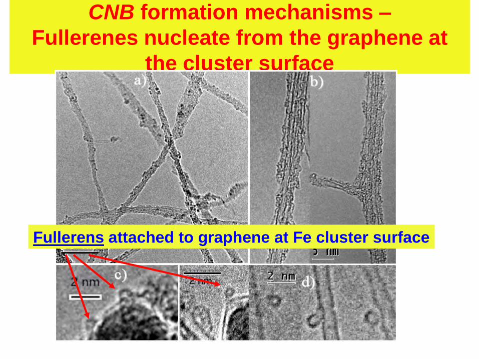
CNB formation mechanisms –
Fullerenes nucleate from the graphene at
the cluster surface
Fullerens attached to graphene at Fe cluster surface
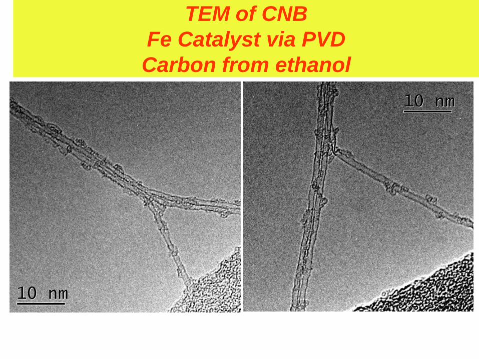
TEM of CNB
Fe Catalyst via PVD
Carbon from ethanol
10 nm10 nm
10 nm10 nm

Conclusion: nothing happened with fullerenes, they were
not dissolved – stronger than Van der Waals bonding
TEM observation of the sample after washing in toluene and decaline
10 nm10 nm 5 nm5 nm
toluene decaline
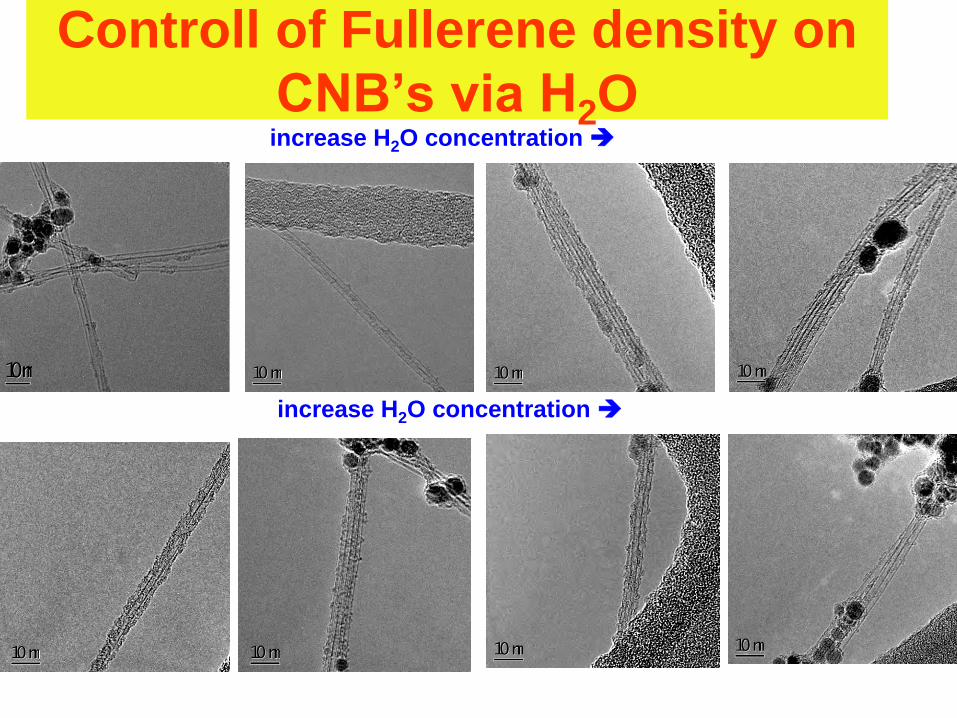
Controll of Fullerene density on
CNB’s via H2O
10 nm10 nm 10 nm10 nm 10 nm10 nm 10 nm10 nm
10 nm10 nm 10 nm10 nm 10 nm10 nm 10 nm10 nm
increase H2O concentration
increase H2O concentration

50
40
30
20
10
0
200 400 600 800 1000 1200
particles
CNTs and fullerenesposi
tion in
react
or, c
m
Temperature, °C
CO
CO
10
0 c
m3 /
min
30
0 c
m3 /
min
water coolingcirculation
ferrocenecartridge
dilutor N2 12 L/min
Filter
water
FT-IR/ ESP
CO
2 o
r N
2
0 -
20
cm
3/m
in
10 nm10 nm
0.2 µm0.2 µm
0.2 µm0.2 µm
A.G.Nasibulin & E.I.Kauppinen et al, Chem.Phys.Lett, 446(2007), 109-114.
885 ºC
945 ºC
2 nm
Synthesis of Carbon NanoBuds
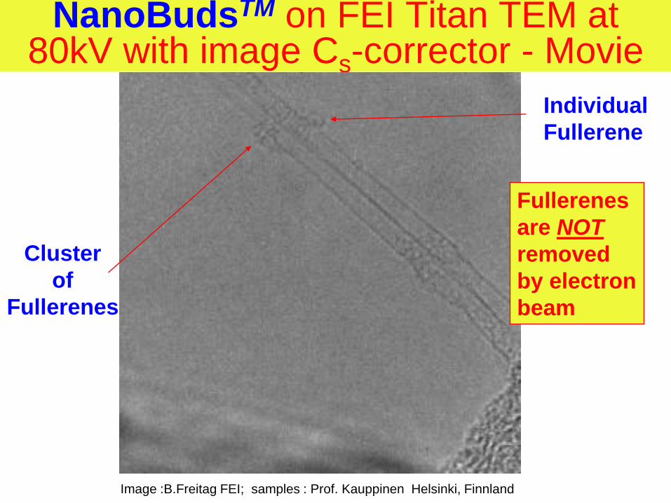
NanoBudsTM on FEI Titan TEM at 80kV with image Cs-corrector - Movie
Image :B.Freitag FEI; samples : Prof. Kauppinen Helsinki, Finnland
Individual
Fullerene
Cluster
of
Fullerenes
Fullerenes
are NOT
removed
by electron
beam

Number size distribution of
NanoBudTM fullerenes measured from
HR-TEM images
0.00
0.05
0.10
0.15
0.20
0.25
0.300.
410.
430.
450.
470.
500.
520.
550.
580.
600.
630.
670.
700.
730.
770.
810.
850.
890.
930.
981.
03
0.390.410.430.450.470.500.520.550.580.600.630.670.700.730.770.810.850.890.930.98Diameter of fullerenes (nm)
Fre
qu
en
cy
C60
C42
C20
C34
C86

Comparison of ultraviolet-visible absorption
spectra of CNB’s, C70 and C60 standards
200 300 400 500 6000.0
0.5
1.0
1.5
2.0
2.5
3.0
3.5
4.0
700 800 900 1000 1100
in hexane: in toluene:
C60
C60
C70
C70
FFCNTs FFCNTs
Absorb
ance (
au)
Wavelength (nm)
SWCNT absortion bands:Fullerene absortion bands:

Raman spectra of NanoBuds carried out by using red (633 nm), green (514 nm), and
blue (488 nm) lasers.
200 400 600 800 1000 1200 1400 1600 1800
0.0
5.0x10³
1.0x10⁴
1.5x10⁴
2.0x10⁴
Inte
nsity (
au
)
Raman shift (cm-1)

Bonding scenarios of fullerenes on
nanotubes based on DFT calculations
Calculations By Arkady
Krasheninnikov, TKK
Nasibulin & Kauppinen et al. Nature Nanotechnology, 2(3) 156 March 2007
LT UHV STM:
Chemisorbed
Fullerene on
Nanotube
Lattice
Peaks in the LDOS
are due to nanobuds,
cannot be assigned to
physisorbed
fullerenesNanometer Range
Controll for DOS !
Ambient STM

Calculations by Arkady
Krasheninnikov, TKK
Experiment
This suggests that
chemically attached
fullerene via 2+2
cycloaddition is
energetically favorable

.
. CNT
Aerosol
Synthesis
Process
Control of Material Direct Manufacture
Deposition
Process
Dry, direct deposition method for Integrated Component Manufacturing
Products
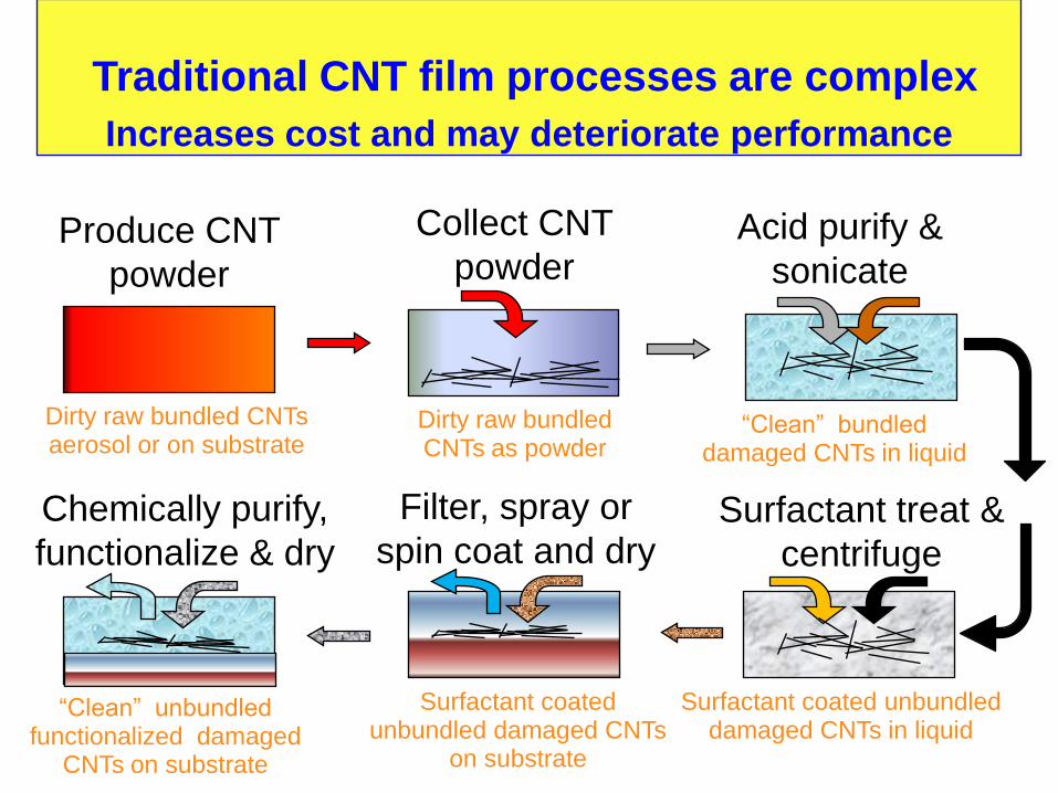
Traditional CNT film processes are complex
Increases cost and may deteriorate performance
Dirty raw bundled CNTs as powder
Collect CNT
powder
“Clean” bundled damaged CNTs in liquid
Acid purify &
sonicateProduce CNT
powder
Dirty raw bundled CNTs aerosol or on substrate
Surfactant coated unbundled damaged CNTs in liquid
Surfactant treat &
centrifuge
“Clean” unbundled functionalized damaged
CNTs on substrate
Chemically purify,
functionalize & dry
Surfactant coated unbundled damaged CNTs
on substrate
Filter, spray or
spin coat and dry
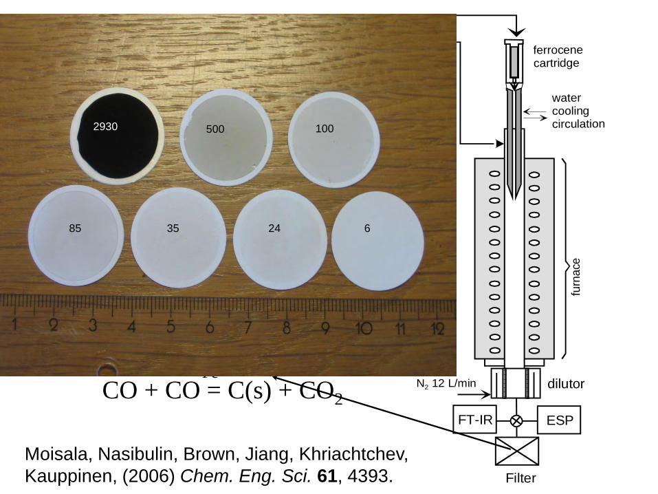
Experimental
set up:
Ferrocene Reactor
CO
CO
100 c
m3 /
min
300 c
m3 /
min
furn
ace
ESP
water coolingcirculation
ferrocenecartridge
dilutor N2 12 L/min
Filter
FT-IR
Moisala, Nasibulin, Brown, Jiang, Khriachtchev,
Kauppinen, (2006) Chem. Eng. Sci. 61, 4393.
Ferrocene: Fe(C5H5)2
Catalyst precursor:
CO + CO = C(s) + CO2
Fe
Carbon source:
6243585
1005002930

Large ReactorSmall Reactor
Flow rate 0.3 liters/min
Reactor Tube Diameter Inner 2.5 cm
Lentgh 50 cmFlow rate 10-100 x Small Reactor

SEM images demonstrating
CNT film densification by ethanol(b)
as deposited CNT film after treatment with ethanol
Nasibulin, Ollikainen, Kauppinen et al. Chem. Engin. J. (2008) 136, 409.

Cold field emission properties of as-deposited CNB
films on Au substrate: comparison with SWCNTs
0.0 0.5 1.0 1.5 2.0 2.50
100
200
300
400
500
600
700
0.0 0.5 1.0 1.5 2.0 2.50
1
2
3
4
SWNTs
NanoBuds (H2O: 65 ppm)
NanoBuds (H2O: 100 ppm)
NanoBuds (H2O: 150 ppm)
C
urr
en
t d
en
sity (
A/c
m2)
Field strength (V/ m)
ACCVD; Tanamura et al., APL (2006)-
SWCNT grown on glass

- Large reactor

Large reactor tubes - HRTEM at 385C

Maria A1 Ethanol treatment heating 485C
Large reactor tubes - HRTEM at 485C

Large reactor tubes - HRTEM at 485C
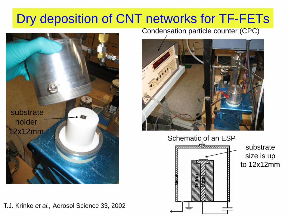
Dry deposition of CNT networks for TF-FETs
Te
flo
n
Me
tal
Schematic of an ESP
substrate
size is up
to 12х12mm
substrate
holder
12х12mm
Meta
l
T.J. Krinke et al., Aerosol Science 33, 2002
Condensation particle counter (CPC)
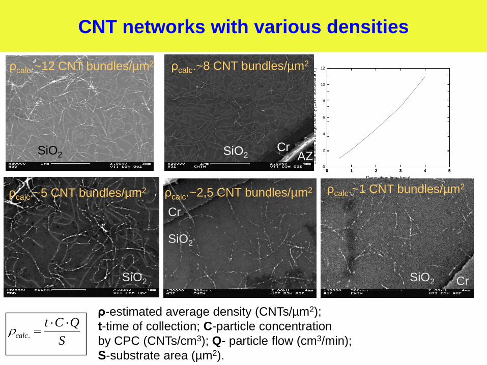
CNT networks with various densities
0 1 2 3 4 5
0
2
4
6
8
10
12
0 1 2 3 4 50
2
4
6
8
10
12
0 1 2 3 4 50
2
4
6
8
10
12
Estim
ate
d a
ve
rag
e d
en
sity [C
NT
bu
nd
les/u
m2]
Deposition time [min]
SiO2
SiO2
Cr
SiO2
ρcalc.~12 CNT bundles/µm2
ρcalc.~5 CNT bundles/µm2 ρcalc.~2,5 CNT bundles/µm2 ρcalc.~1 CNT bundles/µm2
CrSiO2
ρcalc.~8 CNT bundles/µm2
SiO2Cr
AZ
.calc
t C Q
S
ρ-estimated average density (CNTs/µm2);
t-time of collection; C-particle concentration
by CPC (CNTs/cm3); Q- particle flow (cm3/min);
S-substrate area (µm2).

SWCNTN FETs on Si and Kapton substrates –
on/off`= 105, mobility = 5 cm2/(V*s) on Si (L=W=50 µm)
on/off`= 105, mobility = 1cm2/(V*s) on polymer (L=150 µm, W=200 µm)

THANKS TO YOU FOR YOUR
ATTENTION !