Embed Size (px)
Citation preview
Rev
iew
© 2017 WILEY-VCH Verlag GmbH & Co. KGaA, Weinheim wileyonlinelibrary.com (1 of 16) 1603994
Carbon-Based Perovskite Solar Cells without Hole Transport Materials: The Front Runner to the Market?
Haining Chen* and Shihe Yang*
Dr. H. ChenSchool of Materials Science and EngineeringBeihang UniversityNo. 37 Xueyuan Road, Haidian District Beijing 100191, P. R. China E-mail: [email protected]. H. Chen, Prof. S. YangDepartment of ChemistryThe Hong Kong University of Science and TechnologyClear Water BayKowloon, Hong Kong E-mail: [email protected]
DOI: 10.1002/adma.201603994
properties including high absorption coef-ficient,[5,9] high mobility,[10,11] long bal-anced carrier diffusion length[11,12] and low exciton binding energy.[13]
The first well-known PSCs, reported in 2009, exploited the device structure of dye-sensitized solar cells (DSSCs, TiO2/dye/electrolyte) by replacing dye mole-cules with perovskite crystals.[3] However, the significant instability of perovskite in the liquid iodide/iodine redox couple electrolyte led to very poor performance. Then, in 2012, the application of rela-tively stable 2,2,7,7-tetrakis-(N,N-di-p-methoxyphenylamine) 9,9-bifluorene (spiro-OMeTAD) as a hole transport mate-rial (HTM) resulted in a fundamental step change improvement in the device perfor-mance.[14,15] Benefiting from the special properties of perovskite, many organic HTMs have been found to perform well in PSCs, such as poly-triarylamine (PTAA), poly-3-hexylthiophene (P3HT), poly-[2,1,3-benzothiadiazole-4,7-diyl [4 ,4-bis(2-
ethylhexyl)-4H-cyclopenta[2,1-b:3,4-b’]dithiophene-2,6-diyl]] (PCPDTBT), poly-[[9-(1-octylnonyl)-9H-carbazole-2,7-diyl]-2,5-thiophenediyl-2,1,3-benzothiadiazole-4,7-diyl-2,5-thiophen-ediyl] (PCDTBT), etc.[16,17] However, most high-performance organic HTMs are expensive and operationally unstable (and usually require an inert atmosphere). Furthermore, organic HTM layers are usually open and susceptible to migration of halide ions and metal ions (from metal electrode), resulting in degradation.[18] Recently, researchers have proved that perovs-kite (e.g. CH3NH3PbI3) could serve as both a light harvester and a hole transporter,[12,19,20] thus facilitating HTM-free PSCs.[20–25]
Several hole extraction electrodes have been explored for use in HTM-free PSCs, including Au,[19,26] Ni,[27] and carbon.[20,28–30] Among them, carbon is thought to be the most promising for electrode materials as carbon materials are cheap, stable, inert to ion migration originating from perovskite and metal elec-trodes, inherently water-resistant, and therefore advantageous for high device stability.[25,31] As expected, significantly high stability has been reported for carbon-based HTM-free PSCs (C-PSCs), making it among the most promising solar cells for commercialization. During the past few years, much progress has been made on C-PSCs. An increase in PCE from the ini-tial 6.6%[20] to over 14%[32] has been reported, and several novel device structures have been explored. However, the increase in PCE is much slower for C-PSCs than for HTM-based PSCs, and
Organometal trihalide perovskite solar cells (PSCs) have garnered recent interest in the scientific community. In the past few years, they have achieved power conversion efficiencies comparable to traditional commercial solar cells (e.g., crystalline Si, CuInGaSe and CdTe) due to their low-cost of produc-tion via solution-processed fabrication techniques. However, the stability of PSCs must be addressed before their commercialization is viable. Among various kinds of PSCs, carbon-based PSCs without hole transport materials (C-PSCs) seem to be the most promising for addressing the stability issue because carbon materials are stable, inert to ion migration (which originates from perovskite and metal electrodes), and inherently water-resistant. Despite the significant development of C-PSCs since they were first reported in 2013, some pending issues still need to be addressed to increase their commercial competitiveness. Herein, recent developments in C-PSCs, including (1) device structure and working principles, (2) categorical progress of and compar-ison between meso C-PSCs, embedment C-PSCs and paintable PSCs, are reviewed. Promising research directions are then suggested (e.g., materials, interfaces, structure, stability measurement and scaling-up of production) to further improve and promote the commercialization of C-PSCs.
1. Introduction
Organometal trihalide perovskite solar cells (PSCs) have attracted keen attention because of their rapid increase in power conversion efficiency (PCE) in the last few years.[1–8] The latest certified PCE value of 22.1% is approaching that of commercial monocrystalline silicon solar cells.[1] It is unprecedented for a new type of solar cells to demonstrate a comparable performance to traditional commercial solar cells in such a short time. This exceptional performance is due to the hybrid materials (ABX3: A = CH3NH3, HC(NH2)2, Cs; B = Pb, Sn; X = Cl, Br, I), which have been employed for their advantageous optoelectronic
Adv. Mater. 2017, 1603994
www.advancedsciencenews.com www.advmat.de
Rev
iew
© 2017 WILEY-VCH Verlag GmbH & Co. KGaA, Weinheimwileyonlinelibrary.com1603994 (2 of 16)
the gap is getting larger, steadily detracting from the economic advantages of C-PSCs. Therefore, at this point of development, improving the PCE is crucial to improving C-PSCs commercial competitiveness. Since the device structure and working prin-ciple of C-PSCs are different from HTM-based PSCs, some specific and innovative strategies must be employed to improve C-PSCs. Initially, it is necessary to review on the recent pro-gress and state of the art for C-PSCs, focusing on their special structures and properties, in order to make future research efforts more targeted and efficient.
Herein, the device structures of C-PSCs will be reviewed and critically compared to HTM-based PSCs and the special working principles of C-PSCs highlighted. The C-PSCs will be briefly categorized (e.g., meso C-PSCs, embedment C-PSCs and paintable C-PSCs) according to device structure and fab-rication process. The progress will also be discussed and compared in detail. Finally, specific strategies to improve the performance and promote the commercialization of C-PSCs will be discussed.
2. Structure, Working Principles and Evolution of C-PSCs
As illustrated in Figure 1a, the conventional device struc-ture of HTM-based PSCs consists of fluorine-doped tin oxide (FTO)/TiO2 dense layer/TiO2 mesoporous layer/perovskite/HTM/Au.[14,15] Since perovskite has been shown to be an effec-tive hole transporter in addition to being an effective light absorber,[12] PSCs work well even after removal of the HTM layer and direct deposition of an Au electrode on the perovskite layer for hole extraction.[19] Then, by replacing the Au electrode with a C electrode, C-PSCs can and have been fabricated and demonstrated.[20]
Figure 1b depicts the energy level diagram of representative perovskite materials; TiO2, Spiro-OMeTAD, Au and C. For effec-tive hole extraction, the valence band (VB) edge of perovskite should be lower than the highest occupied molecular orbital (HOMO) of the HTM or the Femi levels of Au or C. Therefore, HTM-free PSCs based on MAPbI3, FAPbI3 or MAPbBr3 work well when Au or C electrodes are used. However, either the VB edge of MASnI3 or the Fermi level of the Au or C electrode should be adjusted to match energy level for efficient hole extraction.
In the last six years, the PCE of normal PSCs has experi-enced a rapid increase from 3.8% in 2009[3] to 10.9% in 2012[15] and most recently to 22.1%[1] (Figure 1c). Meanwhile, the PCE of Au-PSCs have increased from an initial 5.5% in 2012[19] to 12.2%.[33] The first reported C-PSCs in 2013 achieved a PCE of about 6.6%.[20] After one year, this increased to 12.8%.[21] The highest reported PCE for a C-PSCs is now 14.5%.[34]
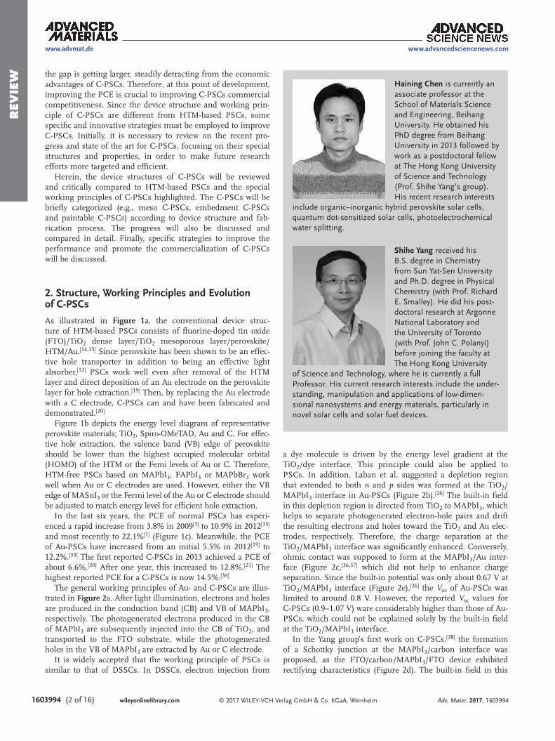
The general working principles of Au- and C-PSCs are illus-trated in Figure 2a. After light illumination, electrons and holes are produced in the conduction band (CB) and VB of MAPbI3, respectively. The photogenerated electrons produced in the CB of MAPbI3 are subsequently injected into the CB of TiO2, and transported to the FTO substrate, while the photogenerated holes in the VB of MAPbI3 are extracted by Au or C electrode.
It is widely accepted that the working principle of PSCs is similar to that of DSSCs. In DSSCs, electron injection from
a dye molecule is driven by the energy level gradient at the TiO2/dye interface. This principle could also be applied to PSCs. In addition, Laban et al. suggested a depletion region that extended to both n and p sides was formed at the TiO2/MAPbI3 interface in Au-PSCs (Figure 2b).[26] The built-in field in this depletion region is directed from TiO2 to MAPbI3, which helps to separate photogenerated electron-hole pairs and drift the resulting electrons and holes toward the TiO2 and Au elec-trodes, respectively. Therefore, the charge separation at the TiO2/MAPbI3 interface was significantly enhanced. Conversely, ohmic contact was supposed to form at the MAPbI3/Au inter-face (Figure 2c,[36,37] which did not help to enhance charge separation. Since the built-in potential was only about 0.67 V at TiO2/MAPbI3 interface (Figure 2e),[26] the Voc of Au-PSCs was limited to around 0.8 V. However, the reported Voc values for C-PSCs (0.9–1.07 V) ware considerably higher than those of Au-PSCs, which could not be explained solely by the built-in field at the TiO2/MAPbI3 interface.
In the Yang group’s first work on C-PSCs,[28] the formation of a Schottky junction at the MAPbI3/carbon interface was proposed, as the FTO/carbon/MAPbI3/FTO device exhibited rectifying characteristics (Figure 2d). The built-in field in this
Haining Chen is currently an associate professor at the School of Materials Science and Engineering, Beihang University. He obtained his PhD degree from Beihang University in 2013 followed by work as a postdoctoral fellow at The Hong Kong University of Science and Technology (Prof. Shihe Yang’s group). His recent research interests
include organic–inorganic hybrid perovskite solar cells, quantum dot-sensitized solar cells, photoelectrochemical water splitting.
Shihe Yang received his B.S. degree in Chemistry from Sun Yat-Sen University and Ph.D. degree in Physical Chemistry (with Prof. Richard E. Smalley). He did his post-doctoral research at Argonne National Laboratory and the University of Toronto (with Prof. John C. Polanyi) before joining the faculty at The Hong Kong University
of Science and Technology, where he is currently a full Professor. His current research interests include the under-standing, manipulation and applications of low-dimen-sional nanosystems and energy materials, particularly in novel solar cells and solar fuel devices.
Adv. Mater. 2017, 1603994
www.advancedsciencenews.comwww.advmat.de

Rev
iew
© 2017 WILEY-VCH Verlag GmbH & Co. KGaA, Weinheim wileyonlinelibrary.com (3 of 16) 1603994
Schottky junction helped to increase the overall built-in poten-tial to 0.85 V (Figure 2f) and presented a direction from MAPbI3 to C electrode, which assisted in separating the photogenerated electron-hole pairs so that resulting holes and electrons could drift toward the C electrode and the TiO2/MAPbI3 interface, respectively. The additional built-in field at the MAPbI3/carbon interface explains the higher Voc and PCE achieved by C-PSCs than Au-PSCs. However, it should be noted that whether or not the Schottky junction was formed at all depends greatly on the Femi level of perovskite and the Femi level of carbon materials.
Yan et al. showed that no obvious Schottky junction was formed at the MAPbI3/single-layer graphene (SG) interface due to the similarity between the Femi level of MAPbI3 and the Femi level of SG.[38] As a result, the C-PSCs based on SG achieved an obviously lower performance than those based on multi-layer gra-phene (MG) that could form a Schottky junction with MAPbI3. Therefore, choosing suitable carbon materials is an important way to form an additional Schottky junction at the MAPbI3/carbon interface and hence to improve device performance.
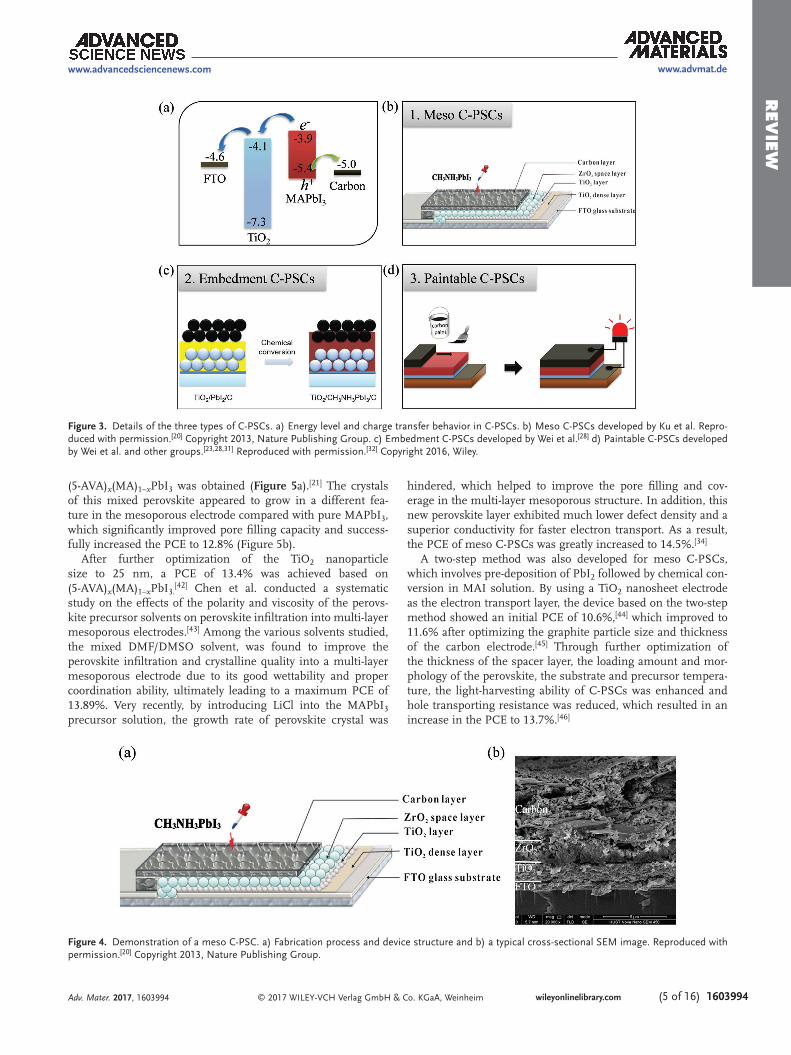
According to their device structure and fabrication procedure, C-PSCs can be divided into three types: meso C-PSCs, embed-ment C-PSCs and paintable C-PSCs (Figure 3). Meso PSCs, developed by Ku et al. (Figure 3b),[20] comprised of an initially deposited multi-layer mesoporous structure, which is subse-quently infiltrated by a perovskite solution. The carbon electrode for meso C-PSCs is typically deposited by doctor blade or screen printing techniques using a carbon paste containing graphite, carbon black and a ZrO2 (or Al2O3) nanoparticle binder, fol-lowed by annealed at high temperature (e.g. 400 °C).[20,39]
Wei et al. explored embedment C-PSCs (Figure 3c),[28] in which a carbon electrode was deposited onto a pre-deposited PbI2 layer, followed by the conversion of PbI2 to MAPbI3. The deposition of a carbon electrode is achieved by direct spin coating of pure carbon materials (e.g. carbon black, carbon nanotube, or graphene) dispersed in non-polar solvents, or by transferring a carbon layer which has been pre-deposited on another substrates followed by drying at low temperature (≤ 100 °C).
Paintable C-PSCs, the third type, were developed as a result of the clamping concept reported in the initial paper on embed-ment C-PSCs (Figure 3d).[23,28,31] The carbon electrode, in paste or paint form (the slurry usually contains graphite, carbon black and a polymer additive) is deposited on a pre-deposited per-ovskite layer using either a painting process or a doctor blade technique, followed by drying at low temperature (e.g. 100 °C). These three types of C-PSCs operate via similar charge trans-port principles, but their different device structures and fabri-cation processes result in different photovoltaic performances. The following section will separately discuss the progress of each type of C-PSC in detail.
3. The Progress of Various C-PSCs
3.1. Meso C-PSCs
The first carbon-based PSC was constructed by Miyasaka et al., and had a low PCE of 0.37%.[40] However, the most famous and
Adv. Mater. 2017, 1603994
www.advancedsciencenews.com www.advmat.de
Figure 1. Device structure and efficiency evaluation of PSCs. a) Device structures of HTM-based PSCs, Au-PSCs and C-PSCs. b) Schematic energy level diagram of perovskite materials, TiO2, Spiro-OMeTAD, Au and C.[20,26,35] c) Reported efficiency evolution of different PSCs.
Rev
iew
© 2017 WILEY-VCH Verlag GmbH & Co. KGaA, Weinheimwileyonlinelibrary.com1603994 (4 of 16)
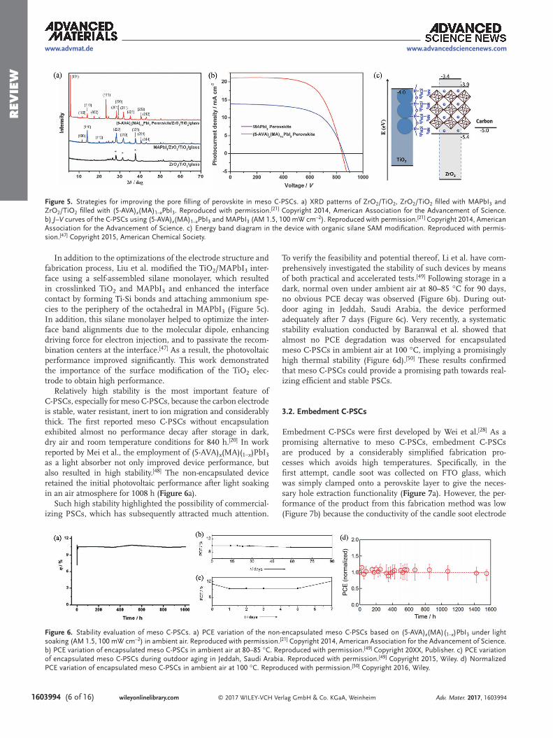
efficient C-PSCs are the meso C-PSCs (Figure 4a) developed by Ku et. al,[20] which have a typical multi-layer mesoporous structure, including TiO2, ZrO2 and carbon mesoporous layers, serving as the electron transporting layer, insulating layer and hole extraction layer, respectively. The TiO2 and ZrO2 mesoporous layers in these meso C-PSCs were fabricated from nanoparticles, while the carbon mesoporous layer (at least sev-eral micrometers thick) was carbon black and layered graphite. The three layers were assembled by screen printing techniques, and subsequent high temperature annealing processes were needed to increase their mechanical strength. Finally, a per-ovskite precursor solution was infiltrated into the multi-layer mesoporous structure by applying the precursor solution dropwise to the surface to obtain the meso C-PSCs. Since the
thickness of the whole device is at least several micrometers, full solution infiltration into the mesoporous electrode is an important issue for meso C-PSCs.
In initial work on meso C-PSCs, a solution of PbI2 and MAI in GBL was applied to the multi-layer mesoporous structure via a one-step deposition method, which obtained a low PCE of 6.6%.[20] The low performance was attributed to the poor penetration of the perovskite solution in the mesoporous electrode. To enhance solution penetration, Xu et al. used an ordered porous carbon material as the carbon electrode, which partially improved the solution penetration and slightly increased the PCE to 7%.[41] In an extension to the study, by introducing HOOC(CH2)4NH3I (5-AVAI) into the precursor solution to partially replace MAI, a mixed perovskite of
Adv. Mater. 2017, 1603994
www.advancedsciencenews.comwww.advmat.de
Figure 2. Working principle of HTM-free PSCs. a) Energy level and charge transfer behavior. b) Schematic band bending diagram at the TiO2/MAPbI3 interface. Reproduced with permission.[26] Copyright 2013, Royal Chemical Society. c) J–V curves of a lateral Au/MAPbI3/Au structure with varying fab-rication temperatures. Reproduced with permission.[36] Copyright 2016, Royal Chemical Society. d) J–V curves of FTO/C/FTO, FTO/MAPbI3/FTO and FTO/C/MAPbI3/FTO devices (inset: proposed equilibrium energy diagram at the C/MAPbI3 interface). Reproduced with permission.[28] Copyright 2014, Royal Chemical Society. e) Mott–Schottky (M–S) curve for Au-PSCs, showing a built-in potential of 0.67 V. Reproduced with permission.[26] Copyright 2013, Royal Chemical Society. f) M–S curve for C-PSCs, presenting a built-in potential of 0.85 V. Reproduced with permission.[28] Copyright 2014, Royal Chemical Society.
Rev
iew
© 2017 WILEY-VCH Verlag GmbH & Co. KGaA, Weinheim wileyonlinelibrary.com (5 of 16) 1603994
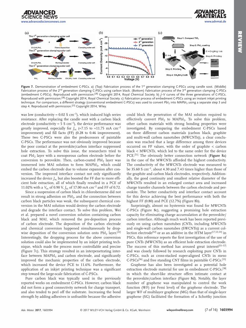
(5-AVA)x(MA)1–xPbI3 was obtained (Figure 5a).[21] The crystals of this mixed perovskite appeared to grow in a different fea-ture in the mesoporous electrode compared with pure MAPbI3, which significantly improved pore filling capacity and success-fully increased the PCE to 12.8% (Figure 5b).
After further optimization of the TiO2 nanoparticle size to 25 nm, a PCE of 13.4% was achieved based on (5-AVA)x(MA)1–xPbI3.
[42] Chen et al. conducted a systematic study on the effects of the polarity and viscosity of the perovs-kite precursor solvents on perovskite infiltration into multi-layer mesoporous electrodes.[43] Among the various solvents studied, the mixed DMF/DMSO solvent, was found to improve the perovskite infiltration and crystalline quality into a multi-layer mesoporous electrode due to its good wettability and proper coordination ability, ultimately leading to a maximum PCE of 13.89%. Very recently, by introducing LiCl into the MAPbI3 precursor solution, the growth rate of perovskite crystal was
hindered, which helped to improve the pore filling and cov-erage in the multi-layer mesoporous structure. In addition, this new perovskite layer exhibited much lower defect density and a superior conductivity for faster electron transport. As a result, the PCE of meso C-PSCs was greatly increased to 14.5%.[34]
A two-step method was also developed for meso C-PSCs, which involves pre-deposition of PbI2 followed by chemical con-version in MAI solution. By using a TiO2 nanosheet electrode as the electron transport layer, the device based on the two-step method showed an initial PCE of 10.6%,[44] which improved to 11.6% after optimizing the graphite particle size and thickness of the carbon electrode.[45] Through further optimization of the thickness of the spacer layer, the loading amount and mor-phology of the perovskite, the substrate and precursor tempera-ture, the light-harvesting ability of C-PSCs was enhanced and hole transporting resistance was reduced, which resulted in an increase in the PCE to 13.7%.[46]
Adv. Mater. 2017, 1603994
www.advancedsciencenews.com www.advmat.de
Figure 3. Details of the three types of C-PSCs. a) Energy level and charge transfer behavior in C-PSCs. b) Meso C-PSCs developed by Ku et al. Repro-duced with permission.[20] Copyright 2013, Nature Publishing Group. c) Embedment C-PSCs developed by Wei et al.[28] d) Paintable C-PSCs developed by Wei et al. and other groups.[23,28,31] Reproduced with permission.[32] Copyright 2016, Wiley.
Figure 4. Demonstration of a meso C-PSC. a) Fabrication process and device structure and b) a typical cross-sectional SEM image. Reproduced with permission.[20] Copyright 2013, Nature Publishing Group.
Rev
iew
© 2017 WILEY-VCH Verlag GmbH & Co. KGaA, Weinheimwileyonlinelibrary.com1603994 (6 of 16)
In addition to the optimizations of the electrode structure and fabrication process, Liu et al. modified the TiO2/MAPbI3 inter-face using a self-assembled silane monolayer, which resulted in crosslinked TiO2 and MAPbI3 and enhanced the interface contact by forming Ti-Si bonds and attaching ammonium spe-cies to the periphery of the octahedral in MAPbI3 (Figure 5c). In addition, this silane monolayer helped to optimize the inter-face band alignments due to the molecular dipole, enhancing driving force for electron injection, and to passivate the recom-bination centers at the interface.[47] As a result, the photovoltaic performance improved significantly. This work demonstrated the importance of the surface modification of the TiO2 elec-trode to obtain high performance.
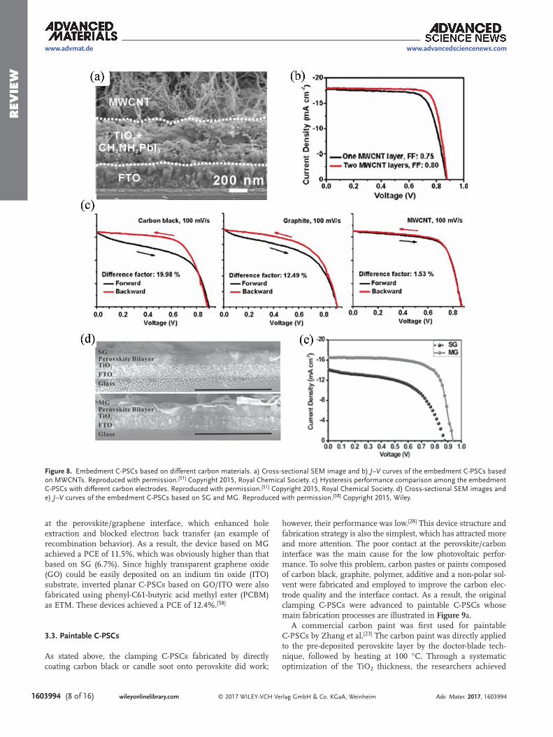
Relatively high stability is the most important feature of C-PSCs, especially for meso C-PSCs, because the carbon electrode is stable, water resistant, inert to ion migration and considerably thick. The first reported meso C-PSCs without encapsulation exhibited almost no performance decay after storage in dark, dry air and room temperature conditions for 840 h.[20] In work reported by Mei et al., the employment of (5-AVA)x(MA)(1–x)PbI3 as a light absorber not only improved device performance, but also resulted in high stability.[48] The non-encapsulated device retained the initial photovoltaic performance after light soaking in an air atmosphere for 1008 h (Figure 6a).
Such high stability highlighted the possibility of commercial-izing PSCs, which has subsequently attracted much attention.
To verify the feasibility and potential thereof, Li et al. have com-prehensively investigated the stability of such devices by means of both practical and accelerated tests.[49] Following storage in a dark, normal oven under ambient air at 80–85 °C for 90 days, no obvious PCE decay was observed (Figure 6b). During out-door aging in Jeddah, Saudi Arabia, the device performed adequately after 7 days (Figure 6c). Very recently, a systematic stability evaluation conducted by Baranwal et al. showed that almost no PCE degradation was observed for encapsulated meso C-PSCs in ambient air at 100 °C, implying a promisingly high thermal stability (Figure 6d).[50] These results confirmed that meso C-PSCs could provide a promising path towards real-izing efficient and stable PSCs.
3.2. Embedment C-PSCs
Embedment C-PSCs were first developed by Wei et al.[28] As a promising alternative to meso C-PSCs, embedment C-PSCs are produced by a considerably simplified fabrication pro-cesses which avoids high temperatures. Specifically, in the first attempt, candle soot was collected on FTO glass, which was simply clamped onto a perovskite layer to give the neces-sary hole extraction functionality (Figure 7a). However, the per-formance of the product from this fabrication method was low (Figure 7b) because the conductivity of the candle soot electrode
Adv. Mater. 2017, 1603994
www.advancedsciencenews.comwww.advmat.de
Figure 5. Strategies for improving the pore filling of perovskite in meso C-PSCs. a) XRD patterns of ZrO2/TiO2, ZrO2/TiO2 filled with MAPbI3 and ZrO2/TiO2 filled with (5-AVA)x(MA)1–xPbI3. Reproduced with permission.[21] Copyright 2014, American Association for the Advancement of Science. b) J–V curves of the C-PSCs using (5-AVA)x(MA)1–xPbI3 and MAPbI3 (AM 1.5, 100 mW cm–2). Reproduced with permission.[21] Copyright 2014, American Association for the Advancement of Science. c) Energy band diagram in the device with organic silane SAM modification. Reproduced with permis-sion.[47] Copyright 2015, American Chemical Society.
Figure 6. Stability evaluation of meso C-PSCs. a) PCE variation of the non-encapsulated meso C-PSCs based on (5-AVA)x(MA)(1–x)PbI3 under light soaking (AM 1.5, 100 mW cm–2) in ambient air. Reproduced with permission.[21] Copyright 2014, American Association for the Advancement of Science. b) PCE variation of encapsulated meso C-PSCs in ambient air at 80–85 °C. Reproduced with permission.[49] Copyright 20XX, Publisher. c) PCE variation of encapsulated meso C-PSCs during outdoor aging in Jeddah, Saudi Arabia. Reproduced with permission.[49] Copyright 2015, Wiley. d) Normalized PCE variation of encapsulated meso C-PSCs in ambient air at 100 °C. Reproduced with permission.[50] Copyright 2016, Wiley.
Rev
iew
© 2017 WILEY-VCH Verlag GmbH & Co. KGaA, Weinheim wileyonlinelibrary.com (7 of 16) 1603994
was low (conductivity ≈ 0.02 S cm–1), which induced high series resistance. After replacing the candle soot with a carbon black electrode (conductivity ≈ 5 S cm–1), the device performance was greatly improved, especially for Jsc (≈7.15 to ≈11.75 mA cm–2 improvement) and fill facto (FF) (0.28 to 0.46 improvement). These two C-PSCs were also the predecessors of paintable C-PSCs. The performance was not obviously improved because the poor contact at the perovskite/carbon interface suppressed hole extraction. To solve this issue, the researchers tried to coat PbI2 layer with a mesoporous carbon electrode before the conversion to perovskite. Then, carbon-coated PbI2 layer was immersed into MAI solution to form MAPbI3, which could embed the carbon electrode due to volume expansion after con-version. The improved interface contact not only significantly increased the device Jsc but also boosted the FF due to more effi-cient hole extraction, all of which finally resulted in a PCE of 11.02% with a Voc of 0.90 V, Jsc of 17.00 mA cm–2 and FF of 0.72.
Since a suspension of carbon black in chlorobenzene did not result in strong adhesion on PbI2, and the connection between carbon black particles was weak, the subsequent chemical con-version in the MAI solution would destroy the carbon electrode and degrade the interface contact. To solve this problem, Wei et al. prepared a novel conversion solution containing carbon black and MAI, which removed the pre-deposition process of carbon electrode. The deposition of the carbon electrode and chemical conversion happened simultaneously by drop-wise deposition of the conversion solution onto PbI2 layer.[22] Interestingly, the dropping process for the above conversion solution could also be implemented by an inkjet printing tech-nique, which made the process more controllable and precise (Figure 7c). This strategy resulted in an interpenetrating inter-face between MAPbI3 and carbon electrode, and significantly improved the mechanic properties of the carbon electrode, which increased the device PCE to 11.6%. Furthermore, the application of an inkjet printing technique was a significant step toward the large-scale fabrication of C-PSCs.
Pure carbon black was typically used in the previously reported works on embedment C-PSCs. However, carbon black did not form a good connectivity network for charge transport, and also tended to peel off the substrate. Increasing the bond strength by adding adhesives is unfeasible because the adhesive
could block the penetration of the MAI solution required to effectively convert PbI2 to MAPbI3. To solve this problem, other carbon materials with strong bonding properties were investigated. By comparing the embedment C-PSCs based on three different carbon materials (carbon black, graphite and multi-wall carbon nanotubes (MWCNTs)), a clear conclu-sion was reached that a large difference among three devices occurred on FF values, with the order of graphite < carbon black < MWCNTs, which led to the same order for the device PCE.[51] The obviously better connection network (Figure 8a) in the case of the MWCNTs afforded the highest conductivity. The conductivity of the MWCNTs electrode was measured to be 35.60 S cm–1, about 4.30 and 7.43 times higher than those of the graphite and carbon black electrodes, respectively. Addition-ally, the good continuity and smallest relative diameter of the MWCNTs resulted in an enlarged contact area and increased charge transfer channels between the carbon electrode and per-ovskite. The better conductivity and interface contact account for this device achieving the best performance with both the highest FF (0.80) and PCE (12.7%) (Figure 8b).
Surprisingly, almost no hysteresis was found for MWCNTs C-PSCs (Figure 8c), suggesting a promising hole extraction capacity for eliminating charge accumulation at the perovskite/carbon interface. Although much work has been reported previ-ously on using carbon nanotubes (CNTs, including MWCNTs and single-wall carbon nanotubes (SWCNTs)) as a current col-lection electrode[52] or as an additive in the HTM layer[17,53,54] in PSCs, this reference reports the first investigation of the use of pure CNTs (MWCNTs) as an efficient hole extraction electrode. The success of this method has aroused great interest[55–57] and was closely followed by research exploiting pure CNTs in C-PSCs, such as cross-stacked super-aligned CNTs in meso C-PSCs[56] and free standing CNT films in paintable C-PSCs.[55]
Graphene has also been investigated as a potential hole extraction electrode material for use in embedment C-PSCs,[38] in which the sheet-like structure offers intimate contact at the perovskite/carbon interface (Figure 8d). Notably, the layer number of graphene was manipulated to control the work function (WF) (or Femi level) of the graphene electrode. The larger WF of multilayer graphene (MG) than that of single-layer graphene (SG) facilitated the formation of a Schottky junction
Adv. Mater. 2017, 1603994
www.advancedsciencenews.com www.advmat.de
Figure 7. Demonstration of embedment C-PSCs. a) (Top) Fabrication process of the 1st generation clamping C-PSCs using candle soot. (Middle) Fabrication process of the 2nd generation clamping C-PSCs using carbon black. (Bottom) Fabrication process of the 3rd generation clamping C-PSCs (embedment C-PSCs). Reproduced with permission.[28] Copyright 2014, Royal Chemical Society. b) J–V curves of the three generations of C-PSCs. Reproduced with permission.[28] Copyright 2014, Royal Chemical Society. c) Fabrication process of embedment C-PSCs using an instant inkjet printing technique. For comparison, a different strategy (conventional embedment C-PSCs) was used to convert PbI2 into MAPbI3 using a separate step 3 and step 4. Reproduced with permission.[22] Copyright 2014, Wiley.
Rev
iew
© 2017 WILEY-VCH Verlag GmbH & Co. KGaA, Weinheimwileyonlinelibrary.com1603994 (8 of 16)
at the perovskite/graphene interface, which enhanced hole extraction and blocked electron back transfer (an example of recombination behavior). As a result, the device based on MG achieved a PCE of 11.5%, which was obviously higher than that based on SG (6.7%). Since highly transparent graphene oxide (GO) could be easily deposited on an indium tin oxide (ITO) substrate, inverted planar C-PSCs based on GO/ITO were also fabricated using phenyl-C61-butyric acid methyl ester (PCBM) as ETM. These devices achieved a PCE of 12.4%.[58]
3.3. Paintable C-PSCs
As stated above, the clamping C-PSCs fabricated by directly coating carbon black or candle soot onto perovskite did work;
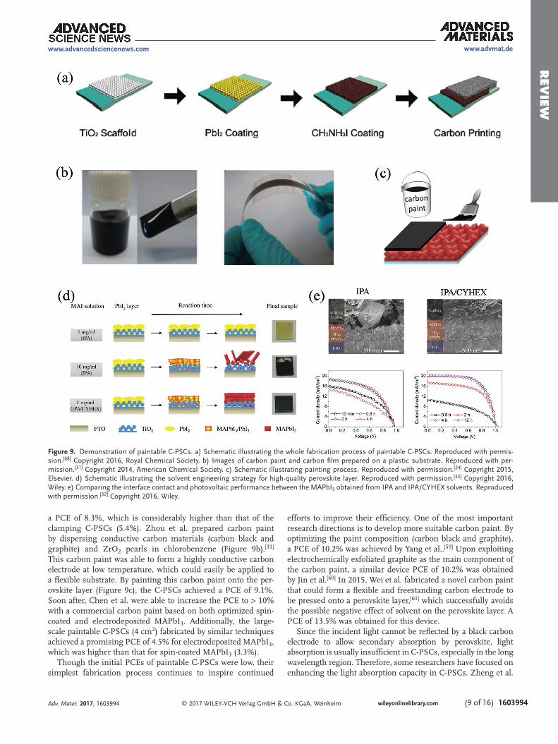
however, their performance was low.[28] This device structure and fabrication strategy is also the simplest, which has attracted more and more attention. The poor contact at the perovskite/carbon interface was the main cause for the low photovoltaic perfor-mance. To solve this problem, carbon pastes or paints composed of carbon black, graphite, polymer, additive and a non-polar sol-vent were fabricated and employed to improve the carbon elec-trode quality and the interface contact. As a result, the original clamping C-PSCs were advanced to paintable C-PSCs whose main fabrication processes are illustrated in Figure 9a.
A commercial carbon paint was first used for paintable C-PSCs by Zhang et al.[23] The carbon paint was directly applied to the pre-deposited perovskite layer by the doctor-blade tech-nique, followed by heating at 100 °C. Through a systematic optimization of the TiO2 thickness, the researchers achieved
Adv. Mater. 2017, 1603994
www.advancedsciencenews.comwww.advmat.de
Figure 8. Embedment C-PSCs based on different carbon materials. a) Cross-sectional SEM image and b) J–V curves of the embedment C-PSCs based on MWCNTs. Reproduced with permission.[51] Copyright 2015, Royal Chemical Society. c) Hysteresis performance comparison among the embedment C-PSCs with different carbon electrodes. Reproduced with permission.[51] Copyright 2015, Royal Chemical Society. d) Cross-sectional SEM images and e) J–V curves of the embedment C-PSCs based on SG and MG. Reproduced with permission.[38] Copyright 2015, Wiley.
Rev
iew
© 2017 WILEY-VCH Verlag GmbH & Co. KGaA, Weinheim wileyonlinelibrary.com (9 of 16) 1603994
a PCE of 8.3%, which is considerably higher than that of the clamping C-PSCs (5.4%). Zhou et al. prepared carbon paint by dispersing conductive carbon materials (carbon black and graphite) and ZrO2 pearls in chlorobenzene (Figure 9b).[31] This carbon paint was able to form a highly conductive carbon electrode at low temperature, which could easily be applied to a flexible substrate. By painting this carbon paint onto the per-ovskite layer (Figure 9c), the C-PSCs achieved a PCE of 9.1%. Soon after, Chen et al. were able to increase the PCE to > 10% with a commercial carbon paint based on both optimized spin-coated and electrodeposited MAPbI3. Additionally, the large-scale paintable C-PSCs (4 cm2) fabricated by similar techniques achieved a promising PCE of 4.5% for electrodeposited MAPbI3, which was higher than that for spin-coated MAPbI3 (3.3%).
Though the initial PCEs of paintable C-PSCs were low, their simplest fabrication process continues to inspire continued
efforts to improve their efficiency. One of the most important research directions is to develop more suitable carbon paint. By optimizing the paint composition (carbon black and graphite), a PCE of 10.2% was achieved by Yang et al..[59] Upon exploiting electrochemically exfoliated graphite as the main component of the carbon paint, a similar device PCE of 10.2% was obtained by Jin et al.[60] In 2015, Wei et al. fabricated a novel carbon paint that could form a flexible and freestanding carbon electrode to be pressed onto a perovskite layer,[61] which successfully avoids the possible negative effect of solvent on the perovskite layer. A PCE of 13.5% was obtained for this device.
Since the incident light cannot be reflected by a black carbon electrode to allow secondary absorption by perovskite, light absorption is usually insufficient in C-PSCs, especially in the long wavelength region. Therefore, some researchers have focused on enhancing the light absorption capacity in C-PSCs. Zheng et al.
Adv. Mater. 2017, 1603994
www.advancedsciencenews.com www.advmat.de
Figure 9. Demonstration of paintable C-PSCs. a) Schematic illustrating the whole fabrication process of paintable C-PSCs. Reproduced with permis-sion.[68] Copyright 2016, Royal Chemical Society. b) Images of carbon paint and carbon film prepared on a plastic substrate. Reproduced with per-mission.[31] Copyright 2014, American Chemical Society. c) Schematic illustrating painting process. Reproduced with permission.[24] Copyright 2015, Elsevier. d) Schematic illustrating the solvent engineering strategy for high-quality perovskite layer. Reproduced with permission.[32] Copyright 2016, Wiley. e) Comparing the interface contact and photovoltaic performance between the MAPbI3 obtained from IPA and IPA/CYHEX solvents. Reproduced with permission.[32] Copyright 2016, Wiley.
Rev
iew
© 2017 WILEY-VCH Verlag GmbH & Co. KGaA, Weinheimwileyonlinelibrary.com1603994 (10 of 16)
investigated the management of light absorption by designing a TiO2 nanobowl array electrode for paintable C-PSCs,[62] which significantly enhanced the light absorption, particularly in the long wavelength region. As a result, the Jsc was increased and the PCE improved to over 12.0%. Bai et al. employed a mixed perovskite of FAxMA1–xPbI3, also to extend light absorption in the long wavelength region (from 780 to 810 nm), which signifi-cantly increased the Jsc from 21.0 to 22.2 mA cm–2 and the PCE from 12.5 to 13.0%, where x = 0.25.[63]
Though much progress has been made in the field of paint-able C-PSCs, the most important issue, the poor contact at the perovskite/carbon interface, is not well addressed. One of the most effective ways to enhance interface contact is to achieve an even perovskite layer. However, the relatively thick TiO2 scaffold (500–800 nm), an essential part in C-PSCs, makes it difficult. The conventional one-step method may produce an even perovskite layer but suffers from poor pore filling and low coverage.[64] Exploiting a mixed γ-butyrolactone/DMSO sol-vent seemed to partially solve this problem with the one-step method, but its beneficial effect was still limited and only a moderate PCE of 11.44% was achieved.[65]
In the two-step method, the full conversion of PbI2 to per-ovskite in MAI IPA solution usually takes a long time,[4,59,66] and tends to generate very large and randomly dispersed per-ovskite crystals on the surface due to the Ostwald ripening pro-cess. Due to the presence of large size graphite particles (in the order of tens of micrometers), the viscosity and fluidity of the carbon paste are high and low, respectively. The large perovs-kite crystals (several micrometers in height) standing out from electrode surface prevent the penetration of the carbon paste to the bottom-layer perovskite crystals, and hence lead to poor interface contact.
Recently, Chen et al. developed a novel solvent engineering strategy based on the two-step method to fabricate pure MAPbI3 with an even surface.[32] As shown in Figure 9d, cyclohexane (CYHEX) was added to a MAI IPA solution to lower the solu-tion polarity, which not only accelerated the chemical conver-sion of PbI2 to MAPbI3 to generate a pure perovskite layer, but also suppressed the Ostwald ripening process to achieve an even surface with a compact capping layer. As a result, this even perovskite layer showed enhanced interface contact with the carbon electrode, which successfully improved the device performance and reproducibility (Figure 9e). The highest PCE of 14.4% was achieved for the small area device, while the large-area device (1 cm2) achieved a PCE of almost 10%. By applying this solvent engineering strategy to MAPbBr3, Chen et al. also obtained an even perovskite layer with conformable oriented crystallization, which resulted in MAPbBr3-based paintable C-PSCs with a record PCE of 8.09% (Voc = 1.35 V).[67] These studies confirm that it is important to enhance interface contact and improve the PCE of paintable C-PSCs by fabricating a high-quality perovskite layer with an even surface.
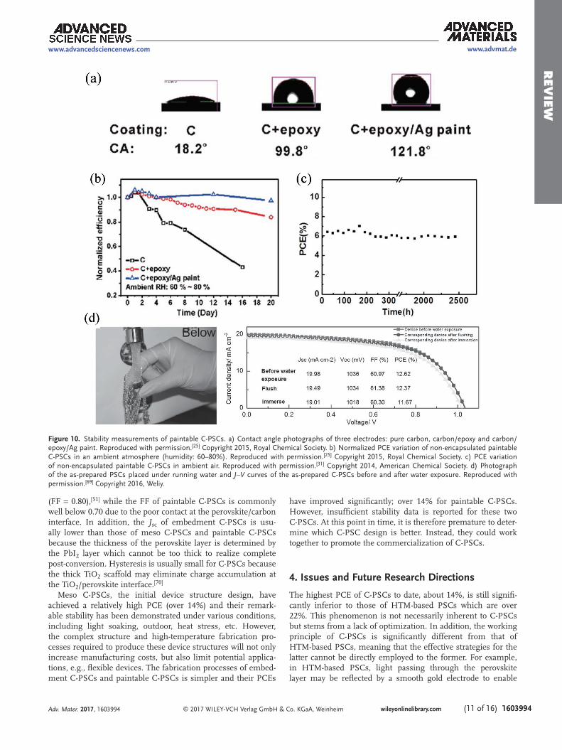
The high stability of paintable C-PSCs has been well demon-strated. In recent work reported by Wei et al., carbon electrodes with and without epoxy, and with and without a Ag coating were thoroughly compared.[25] Epoxy, a common polymer in carbon paint, showed good water resistance. Therefore, the carbon electrode prepared from carbon paint exhibited higher hydrophobicity compared with the bare carbon electrode
(Figure 10a). This hydrophobicity was enhanced by coating the carbon electrode with Ag paint, which was used to further increase the conductivity of carbon electrode. Since perovskite is very sensitive to moisture, water repellency becomes very important for the device stability. Environmental stability meas-urements of the non-encapsulated C-PSCs stored in ambient atmosphere (humidity: 60–80%) indicated a higher stability for C-PSCs with epoxy in the carbon electrode, which was further improved by the Ag coating. These devices exhibited almost no PCE decay after 20 days (Figure 10b).
Even more promising results have been reported by other researchers. Zhang et al. observed almost no performance decay for paintable C-PSCs produced using a commercial carbon paint,[23] while a custom carbon paint developed by Zhou et al. resulted in no PCE decay of a non-encapsulated device after 2446 h (Figure 10c).[31] Furthermore, Yu et al. dem-onstrated that about 98 and 92% of the initial PCE of their devices were retained after water exposure by flushing and immersion (Figure 10d), respectively, due to the hydrophobicity of carbon electrode.[69] Though many reported paintable C-PSCs have shown excellent stability, stability tests under representa-tive practical conditions, such as light soaking condition, high temperature (e.g. 80 °C), etc., is still lacking.
3.4. Comparison of Various C-PSCs
The various device structures of C-PSCs have led to consider-able differences in fabrication processes, particularly regarding the techniques for deposition of the metal oxide scaffold and carbon electrode. Deposition techniques of the perovskite layer for different C-PSCs are also significantly different. The multi-layer mesoporous structure, comprising at least several micrometers in meso C-PSCs hinders the complete conversion of pre-deposited PbI2. As such, the one-step method of perovs-kite deposition is more suitable for meso C-PSCs. For embed-ment C-PSCs, the pre-deposited PbI2 is needed to separate the carbon electrode and TiO2 scaffold, which can only be realized by the two-step method. In the fabrication of paintable C-PSCs, the carbon electrode is layered on after the perovskite deposi-tion. Therefore, both the one-step and two-step methods are feasible, and other methods developed for HTM-based PSCs can also be directly employed.
Large differences in some photovoltaic parameters have been observed for different C-PSCs though their PCEs are compa-rable. Due to the low hole selectivity of the carbon electrode, high charge recombination happens at the perovskite/carbon interface. The C-PSCs based on pure carbon electrodes, namely meso C-PSCs and embedment C-PSCs, commonly achieve low Voc (around 0.9 V). In contrast, polymer in carbon paste based paintable C-PSCs tend to form a thin tunneling insu-lating polymer layer at the perovskite/carbon interface, which could prevent electron transfer from perovskite to carbon and hence suppress charge recombination.[25] As such, higher Voc results are obtained for paintable C-PSCs (e.g. over 1 V). Since the carbon electrodes are embedded in the perovskite layers for both meso C-PSCs and embedment C-PSCs, hole extrac-tion is efficient and results in high FF (over 0.70), especially for embedment C-PSCs based on carbon nanotube electrode
Adv. Mater. 2017, 1603994
www.advancedsciencenews.comwww.advmat.de
Rev
iew
© 2017 WILEY-VCH Verlag GmbH & Co. KGaA, Weinheim wileyonlinelibrary.com (11 of 16) 1603994
(FF = 0.80),[51] while the FF of paintable C-PSCs is commonly well below 0.70 due to the poor contact at the perovskite/carbon interface. In addition, the Jsc of embedment C-PSCs is usu-ally lower than those of meso C-PSCs and paintable C-PSCs because the thickness of the perovskite layer is determined by the PbI2 layer which cannot be too thick to realize complete post-conversion. Hysteresis is usually small for C-PSCs because the thick TiO2 scaffold may eliminate charge accumulation at the TiO2/perovskite interface.[70]
Meso C-PSCs, the initial device structure design, have achieved a relatively high PCE (over 14%) and their remark-able stability has been demonstrated under various conditions, including light soaking, outdoor, heat stress, etc. However, the complex structure and high-temperature fabrication pro-cesses required to produce these device structures will not only increase manufacturing costs, but also limit potential applica-tions, e.g., flexible devices. The fabrication processes of embed-ment C-PSCs and paintable C-PSCs is simpler and their PCEs
have improved significantly; over 14% for paintable C-PSCs. However, insufficient stability data is reported for these two C-PSCs. At this point in time, it is therefore premature to deter-mine which C-PSC design is better. Instead, they could work together to promote the commercialization of C-PSCs.
4. Issues and Future Research Directions
The highest PCE of C-PSCs to date, about 14%, is still signifi-cantly inferior to those of HTM-based PSCs which are over 22%. This phenomenon is not necessarily inherent to C-PSCs but stems from a lack of optimization. In addition, the working principle of C-PSCs is significantly different from that of HTM-based PSCs, meaning that the effective strategies for the latter cannot be directly employed to the former. For example, in HTM-based PSCs, light passing through the perovskite layer may be reflected by a smooth gold electrode to enable
Adv. Mater. 2017, 1603994
www.advancedsciencenews.com www.advmat.de
Figure 10. Stability measurements of paintable C-PSCs. a) Contact angle photographs of three electrodes: pure carbon, carbon/epoxy and carbon/epoxy/Ag paint. Reproduced with permission.[25] Copyright 2015, Royal Chemical Society. b) Normalized PCE variation of non-encapsulated paintable C-PSCs in an ambient atmosphere (humidity: 60–80%). Reproduced with permission.[25] Copyright 2015, Royal Chemical Society. c) PCE variation of non-encapsulated paintable C-PSCs in ambient air. Reproduced with permission.[31] Copyright 2014, American Chemical Society. d) Photograph of the as-prepared PSCs placed under running water and J–V curves of the as-prepared C-PSCs before and after water exposure. Reproduced with permission.[69] Copyright 2016, Weliy.
Rev
iew
© 2017 WILEY-VCH Verlag GmbH & Co. KGaA, Weinheimwileyonlinelibrary.com1603994 (12 of 16)
secondary absorption, which helps to reduce the thickness of perovskite layer (400–600 nm).[6,71] However, black carbon elec-trodes cannot reflect passing light, and hence a thicker perovs-kite layer (around 1 µm)[32,33] is needed to enable complete light absorption. Additionally, the TiO2/perovskite interface is the only effective charge separation interface in C-PSCs. Therefore, the TiO2 layer needs to be made porous and its thicknesses obviously larger (400–600 nm)[23,30,72] than those in HTM-based PSCs (100–200 nm).[4,6] These unique features of C-PSCs indi-cate that new and different strategies are necessary to increase the PCE of these devices.
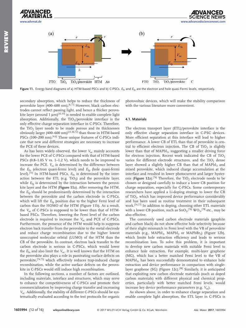
As has been widely observed, the lower Voc mainly accounts for the lower PCE of C-PSCs compared with that of HTM-based PSCs (0.8–1.05 V vs. 1–1.2 V), which needs to be improved to increase the PCE. Voc is determined by the difference between the Efn (electron quasi-fermi level) and Efp (hole quasi-fermi level).[73] In HTM-based PSCs, Efn is determined by the inter-action between the ETL (e.g. TiO2) and the perovskite layer, while Efp is determined by the interaction between the perovs-kite layer and the HTM (Figure 11a). After removing the HTM, the Efp should be predominantly determined by the interaction between the perovskite and the carbon electrode in C-PSCs, which will lift the Efp position due to the higher Femi level of carbon than the HOMO of the HTM (Figure 11b). As a result, the Voc of C-PSCs is supposed to be lower than that of HTM-based PSCs. Therefore, lowering the Femi level of the carbon electrode is required to increase the Voc and PCE of C-PSCs. Furthermore, the presence of the HTM would help to suppress electron back transfer from the perovskite to the metal electrode and reduce charge recombination due to the higher lowest unoccupied molecular orbital (LUMO) of the HTM than the CB of the perovskite. In contrast, electron back transfer to the carbon electrode is serious in C-PSCs, which would lower the Efn and also limit the Voc. It is well known that the HTM on the perovskite also plays a role in passivating surface defects on perovskite,[74,75] which effectively reduces trap-induced charge recombination, while the active surface defects on the perovs-kite in C-PSCs would still induce high recombination.
In the following sections, a number of factors are outlined, including materials, interface and structures, which may serve to enhance the competitiveness of C-PSCs and promote their commercialization by improving charge transfer and increasing Voc. Additionally, the stability of different C-PSCs should be sys-tematically evaluated according to the test protocols for organic
photovoltaic devices, which will make the stability comparison with the various literature more convenient.
4.1. Materials
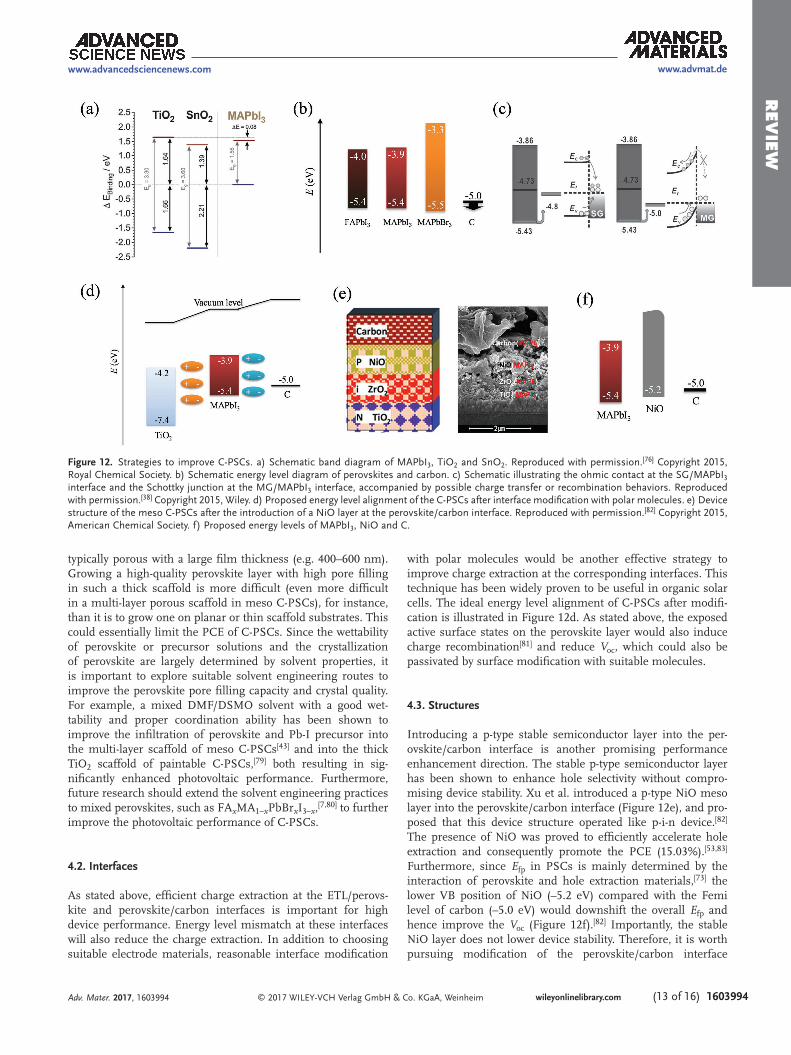
The electron transport layer (ETL)/perovskite interface is the only effective charge separation interface in C-PSC devices. More efficient separation at this interface will lead to higher performance. A lower CB of ETL than that of perovskite is cen-tral to efficient electron injection. The CB of TiO2 is slightly lower than that of MAPbI3, suggesting a smaller driving force for electron injection. Recent work indicated the CB of TiO2 varies for different electrode structures, and the TiO2 dense layer showed a slightly higher CB than that of MAPbI3 and mixed perovskite, which induced charge accumulation at the interface and resulted in lower photocurrent and larger hyster-esis (Figure 12a).[76] Therefore, the TiO2 electrode needs to be chosen or designed carefully to induce a lower CB position for charge separation, especially for C-PSCs. Some contemporary researchers have applied a Li-doping strategy to lower the CB of TiO2, which has improved device performance considerably and has been used as routine treatment in their subsequent work.[74,77] In addition to doping, choosing other ETL materials with a lower CB position, such as SnO2,[76] WO3,[78] etc., may be also effective.
The commonly used carbon electrode materials (graphite and carbon black) do not show effective hole selectivity because of their slight mismatch in Femi level with the VB of perovskite materials (e.g., MAPbI3, MAPbI3 or MAPbBr3) (Figure 12b), which limits hole extraction efficiency and leads to serious recombination loss. To solve this problem, it is important to develop new carbon materials with suitable Femi level to enhance hole extraction. For example, multi-layer graphene (MG), which has a better matched Femi level to the VB of MAPbI3, has been successfully demonstrated to enhance hole extraction and device performance in comparison with single-layer graphene (SG) (Figure 12c).[38] Similarly, it is anticipated that exploiting new carbon electrode materials (such as doped carbon materials) with different physical and chemical prop-erties, particularly with better matched Femi levels, would increase key device performance parameters (e.g. Voc).
As shown above, in order to enhance charge separation and enable complete light absorption, the ETL layer in C-PSCs is
Adv. Mater. 2017, 1603994
www.advancedsciencenews.comwww.advmat.de
Figure 11. Energy band diagrams of a) HTM-based PSCs and b) C-PSCs. Efn and Efp are the electron and hole quasi-Fermi levels, respectively.
Rev
iew
© 2017 WILEY-VCH Verlag GmbH & Co. KGaA, Weinheim wileyonlinelibrary.com (13 of 16) 1603994Adv. Mater. 2017, 1603994
www.advancedsciencenews.com www.advmat.de
typically porous with a large film thickness (e.g. 400–600 nm). Growing a high-quality perovskite layer with high pore filling in such a thick scaffold is more difficult (even more difficult in a multi-layer porous scaffold in meso C-PSCs), for instance, than it is to grow one on planar or thin scaffold substrates. This could essentially limit the PCE of C-PSCs. Since the wettability of perovskite or precursor solutions and the crystallization of perovskite are largely determined by solvent properties, it is important to explore suitable solvent engineering routes to improve the perovskite pore filling capacity and crystal quality. For example, a mixed DMF/DSMO solvent with a good wet-tability and proper coordination ability has been shown to improve the infiltration of perovskite and Pb-I precursor into the multi-layer scaffold of meso C-PSCs[43] and into the thick TiO2 scaffold of paintable C-PSCs,[79] both resulting in sig-nificantly enhanced photovoltaic performance. Furthermore, future research should extend the solvent engineering practices to mixed perovskites, such as FAxMA1–xPbBrxI3–x,[7,80] to further improve the photovoltaic performance of C-PSCs.
4.2. Interfaces
As stated above, efficient charge extraction at the ETL/perovs-kite and perovskite/carbon interfaces is important for high device performance. Energy level mismatch at these interfaces will also reduce the charge extraction. In addition to choosing suitable electrode materials, reasonable interface modification
with polar molecules would be another effective strategy to improve charge extraction at the corresponding interfaces. This technique has been widely proven to be useful in organic solar cells. The ideal energy level alignment of C-PSCs after modifi-cation is illustrated in Figure 12d. As stated above, the exposed active surface states on the perovskite layer would also induce charge recombination[81] and reduce Voc, which could also be passivated by surface modification with suitable molecules.
4.3. Structures
Introducing a p-type stable semiconductor layer into the per-ovskite/carbon interface is another promising performance enhancement direction. The stable p-type semiconductor layer has been shown to enhance hole selectivity without compro-mising device stability. Xu et al. introduced a p-type NiO meso layer into the perovskite/carbon interface (Figure 12e), and pro-posed that this device structure operated like p-i-n device.[82] The presence of NiO was proved to efficiently accelerate hole extraction and consequently promote the PCE (15.03%).[53,83] Furthermore, since Efp in PSCs is mainly determined by the interaction of perovskite and hole extraction materials,[73] the lower VB position of NiO (–5.2 eV) compared with the Femi level of carbon (–5.0 eV) would downshift the overall Efp and hence improve the Voc (Figure 12f).[82] Importantly, the stable NiO layer does not lower device stability. Therefore, it is worth pursuing modification of the perovskite/carbon interface
Figure 12. Strategies to improve C-PSCs. a) Schematic band diagram of MAPbI3, TiO2 and SnO2. Reproduced with permission.[76] Copyright 2015, Royal Chemical Society. b) Schematic energy level diagram of perovskites and carbon. c) Schematic illustrating the ohmic contact at the SG/MAPbI3 interface and the Schottky junction at the MG/MAPbI3 interface, accompanied by possible charge transfer or recombination behaviors. Reproduced with permission.[38] Copyright 2015, Wiley. d) Proposed energy level alignment of the C-PSCs after interface modification with polar molecules. e) Device structure of the meso C-PSCs after the introduction of a NiO layer at the perovskite/carbon interface. Reproduced with permission.[82] Copyright 2015, American Chemical Society. f) Proposed energy levels of MAPbI3, NiO and C.
Rev
iew
© 2017 WILEY-VCH Verlag GmbH & Co. KGaA, Weinheimwileyonlinelibrary.com1603994 (14 of 16) Adv. Mater. 2017, 1603994
www.advancedsciencenews.comwww.advmat.de
in C-PSCs with a stable p-type semiconductor layer (e.g., CuSCN,[84] CuI,[85] etc.) to enhance hole extraction without com-promising device stability.
4.4. Stability Testing
Higher device stability has been proven for C-PSCs in com-parison with HTM-based PSCs, especially for meso C-PSCs. However, stability tests on C-PSCs are still significantly lacking and test conditions vary largely in the literature, which limits the effective assessment of stability results and confuses the application prospects. No stability test protocol has been estab-lished for PSCs. For convenience, the stability testing protocols for organic photovoltaic materials and devices could be used as a reference. In the protocols, there are several categories of test methods, such as dark, outdoor, simulated light and stress, and thermal cycling. Each category can be subdivided into three levels: Basic (Level 1), Intermediate (Level 2) and Advanced (Level 3).[86] It is recommended that researchers perform and report stability measurements according to these protocols in the future, which would immediately allow others to assess the value of the data.
4.5. Scaling Up
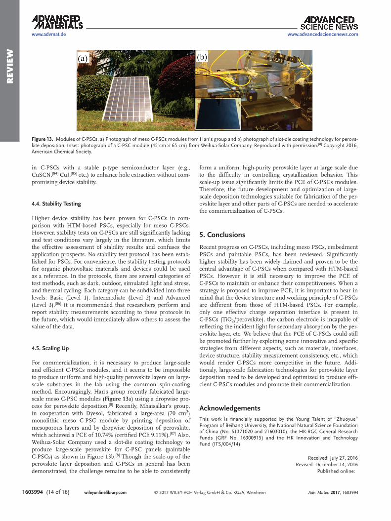
For commercialization, it is necessary to produce large-scale and efficient C-PSCs modules, and it seems to be impossible to produce uniform and high-quality perovskite layers on large-scale substrates in the lab using the common spin-coating method. Encouragingly, Han’s group recently fabricated large-scale meso C-PSC modules (Figure 13a) using a dropwise pro-cess for perovskite deposition.[8] Recently, Mhaisalkar’s group, in cooperation with Dyesol, fabricated a large-area (70 cm2) monolithic meso C-PSC module by printing deposition of mesoporous layers and by dropwise deposition of perovskite, which achieved a PCE of 10.74% (certified PCE 9.11%).[87] Also, Weihua-Solar Company used a slot-die coating technology to produce large-scale perovskite for C-PSC panels (paintable C-PSCs) as shown in Figure 13b.[8] Though the scale-up of the perovskite layer deposition and C-PSCs in general has been demonstrated, the challenge remains to be able to consistently
form a uniform, high-purity perovskite layer at large scale due to the difficulty in controlling crystallization behavior. This scale-up issue significantly limits the PCE of C-PSCs modules. Therefore, the future development and optimization of large-scale deposition technologies suitable for fabrication of the per-ovskite layer and other parts of C-PSCs are needed to accelerate the commercialization of C-PSCs.
5. Conclusions
Recent progress on C-PSCs, including meso PSCs, embedment PSCs and paintable PSCs, has been reviewed. Significantly higher stability has been widely claimed and proven to be the central advantage of C-PSCs when compared with HTM-based PSCs. However, it is still necessary to improve the PCE of C-PSCs to maintain or enhance their competitiveness. When a strategy is proposed to improve PCE, it is important to bear in mind that the device structure and working principle of C-PSCs are different from those of HTM-based PSCs. For example, only one effective charge separation interface is present in C-PSCs (TiO2/perovskite), the carbon electrode is incapable of reflecting the incident light for secondary absorption by the per-ovskite layer, etc. We believe that the PCE of C-PSCs could still be promoted further by exploiting some innovative and specific strategies from different aspects, such as materials, interfaces, device structure, stability measurement consistency, etc., which would render C-PSCs more competitive in the future. Addi-tionaly, large-scale fabrication technologies for perovskite layer deposition need to be developed and optimized to produce effi-cient C-PSCs modules and promote their commercialization.
AcknowledgementsThis work is financially supported by the Young Talent of “Zhuoyue” Program of Beihang University, the National Natural Science Foundation of China (No. 51371020 and 21603010), the HK-RGC General Research Funds (GRF No. 16300915) and the HK Innovation and Technology Fund (ITS/004/14).
Received: July 27, 2016Revised: December 14, 2016
Published online:
Figure 13. Modules of C-PSCs. a) Photograph of meso C-PSCs modules from Han’s group and b) photograph of slot-die coating technology for perovs-kite deposition. Inset: photograph of a C-PSC module (45 cm × 65 cm) from Weihua-Solar Company. Reproduced with permission.[8] Copyright 2016, American Chemical Society.
Rev
iew
© 2017 WILEY-VCH Verlag GmbH & Co. KGaA, Weinheim wileyonlinelibrary.com (15 of 16) 1603994Adv. Mater. 2017, 1603994
www.advancedsciencenews.com www.advmat.de
[1] National Revewable Energy Laboratory (NREL), http://www.nrel.gov/ncpv/images/efficiency_chart.jpg 2016, (accessed: September 2016).
[2] a) X. Li, D. Bi, C. Yi, J. D. Decoppet, J. Luo, S. M. Zakeeruddin, A. Hagfeldt, M. Gratzel, Science 2016, 353, 58; b) Y. Bai, H. N. Chen, S. Xiao, Q. F. Xue, T. Zhang, Z. L. Zhu, Q. Li, C. Hu, Y. Yang, Z. C. Hu, F. Huang, K. S. Wong, H. L. Yip, S. H. Yang, Adv. Funct. Mater. 2016, 26, 2950; c) K. Yan, M. Long, T. Zhang, Z. Wei, H. Chen, S. Yang, J. Xu, J. Am. Chem. Soc. 2015, 137, 4460; d) T. Zhang, H. Chen, Y. Bai, S. Xiao, L. Zhu, C. Hu, Q. Xue, S. Yang, Nano Energy 2016, 26, 620.
[3] A. Kojima, K. Teshima, Y. Shirai, T. Miyasaka, J. Am. Chem. Soc. 2009, 131, 6050.
[4] W. S. Yang, J. H. Noh, N. J. Jeon, Y. C. Kim, S. Ryu, J. Seo, S. I. Seok, Science 2015, 348, 1234.
[5] J. H. Im, I. H. Jang, N. Pellet, M. Gratzel, N. G. Park, Nat. Nanotechnol. 2014, 9, 927.
[6] N. J. Jeon, J. H. Noh, Y. C. Kim, W. S. Yang, S. Ryu, S. I. Seok, Nat. Mater. 2014, 13, 897.
[7] a) D. Bi, W. Tress, M. I. Dar, P. Gao, J. Luo, C. Renevier, K. Schenk, A. Abate, F. Giordano, J. P. Correa Baena, J. D. Decoppet, S. M. Zakeeruddin, M. K. Nazeeruddin, M. Gratzel, A. Hagfeldt, Sci. Adv. 2016, 2, e1501170; b) D. Bi, C. Yi, J. Luo, J.-D. Décoppet, F. Zhang, S. M. Zakeeruddin, X. Li, A. Hagfeldt, M. Grätzel, Nat. Energy 2016, 1, 16142.
[8] Y. Zhou, K. Zhu, ACS Energy Lett. 2016, 1, 64.[9] S. Y. Sun, T. Salim, N. Mathews, M. Duchamp, C. Boothroyd,
G. C. Xing, T. C. Sum, Y. M. Lam, Energy Environ. Sci. 2014, 7, 399.[10] a) C. S. Ponseca Jr., T. J. Savenije, M. Abdellah, K. Zheng, A. Yartsev,
T. Pascher, T. Harlang, P. Chabera, T. Pullerits, A. Stepanov, J. P. Wolf, V. Sundstrom, J. Am. Chem. Soc. 2014, 136, 5189; b) K.-G. Lim, S. Ahn, Y.-H. Kim, Y. Qi, T.-W. Lee, Energy Environ. Sci. 2016, 9, 932.
[11] a) Q. Dong, Y. Fang, Y. Shao, P. Mulligan, J. Qiu, L. Cao, J. Huang, Science 2015, 347, 967; b) D. Shi, V. Adinolfi, R. Comin, M. Yuan, E. Alarousu, A. Buin, Y. Chen, S. Hoogland, A. Rothenberger, K. Katsiev, Y. Losovyj, X. Zhang, P. A. Dowben, O. F. Mohammed, E. H. Sargent, O. M. Bakr, Science 2015, 347, 519.
[12] a) S. D. Stranks, G. E. Eperon, G. Grancini, C. Menelaou, M. J. Alcocer, T. Leijtens, L. M. Herz, A. Petrozza, H. J. Snaith, Science 2013, 342, 341; b) G. Xing, N. Mathews, S. Sun, S. S. Lim, Y. M. Lam, M. Gratzel, S. Mhaisalkar, T. C. Sum, Science 2013, 342, 344.
[13] V. D’Innocenzo, G. Grancini, M. J. Alcocer, A. R. Kandada, S. D. Stranks, M. M. Lee, G. Lanzani, H. J. Snaith, A. Petrozza, Nat. Commun. 2014, 5, 3586.
[14] H. S. Kim, C. R. Lee, J. H. Im, K. B. Lee, T. Moehl, A. Marchioro, S. J. Moon, R. Humphry-Baker, J. H. Yum, J. E. Moser, M. Gratzel, N. G. Park, Sci. Rep. 2012, 2, 591.
[15] M. M. Lee, J. Teuscher, T. Miyasaka, T. N. Murakami, H. J. Snaith, Science 2012, 338, 643.
[16] a) J. H. Heo, S. H. Im, J. H. Noh, T. N. Mandal, C. S. Lim, J. A. Chang, Y. H. Lee, H. J. Kim, A. Sarkar, M. K. Nazeeruddin, M. Gratzel, S. I. Seok, Nat. Photonics 2013, 7, 487; b) J. Seo, N. J. Jeon, W. S. Yang, H. W. Shin, T. K. Ahn, J. Lee, J. H. Noh, S. I. Seok, Adv. Energy Mater. 2015, 5, 1501320; c) J. Y. Xiao, J. J. Shi, H. B. Liu, Y. Z. Xu, S. T. Lv, Y. H. Luo, D. M. Li, Q. B. Meng, Y. L. Li, Adv. Energy Mater. 2015, 5, 1401943; d) H. Chen, S. Yang, Nanoscale Horiz. 2016; e) P. Qin, S. Paek, M. I. Dar, N. Pellet, J. Ko, M. Gratzel, M. K. Nazeeruddin, J. Am. Chem. Soc. 2014, 136, 8516; f) P. Gratia, A. Magomedov, T. Malinauskas, M. Daskeviciene, A. Abate, S. Ahmad, M. Gratzel, V. Getautis, M. K. Nazeeruddin, Angew. Chem. 2015, 54, 11409; g) H.-C. Liao, T. L. D. Tam, P. Guo, Y. Wu, E. F. Manley, W. Huang, N. Zhou, C. M. M. Soe, B. Wang, M. R. Wasielewski, L. X. Chen, M. G. Kanatzidis, A. Facchetti,
R. P. H. Chang, T. J. Marks, Adv. Energy Mater. 2016, 6, 1600502; h) M. Saliba, S. Orlandi, T. Matsui, S. Aghazada, M. Cavazzini, J.-P. Correa-Baena, P. Gao, R. Scopelliti, E. Mosconi, K.-H. Dahmen, F. De Angelis, A. Abate, A. Hagfeldt, G. Pozzi, M. Graetzel, M. K. Nazeeruddin, Nat. Energy 2016, 1, 15017.
[17] X. Zheng, H. Chen, Z. Wei, Y. Yang, H. Lin, S. Yang, Front. Optoelec-tron. 2016, 9, 71.
[18] a) T. A. Berhe, W. N. Su, C. H. Chen, C. J. Pan, J. H. Cheng, H. M. Chen, M. C. Tsai, L. Y. Chen, A. A. Dubale, B. J. Hwang, Energy Environ. Sci. 2016, 9, 323; b) P. Docampo, T. Bein, Acc. Chem. Res. 2016, 49, 339; c) M. Shahbazi, H. Wang, Sol. Energy 2016, 123, 74; d) D. Wang, M. Wright, N. K. Elumalai, A. Uddin, Sol. Energy Mater. Sol. Cells 2016, 147, 255; e) M. D. Ye, X. D. Hong, F. Y. Zhang, X. Y. Liu, J. Mater. Chem. A 2016, 4, 6755; f) H. Back, G. Kim, J. Kim, J. Kong, T. K. Kim, H. Kang, H. Kim, J. Lee, S. Lee, K. Lee, Energy Environ. Sci. 2016, 9, 1258; g) K. Domanski, J.-P. Correa-Baena, N. Mine, M. K. Nazeeruddin, A. Abate, M. Saliba, W. Tress, A. Hagfeldt, M. Grätzel, ACS Nano 2016, 10, 6306.
[19] L. Etgar, P. Gao, Z. Xue, Q. Peng, A. K. Chandiran, B. Liu, M. K. Nazeeruddin, M. Gratzel, J. Am. Chem. Soc. 2012, 134, 17396.
[20] Z. Ku, Y. Rong, M. Xu, T. Liu, H. Han, Sci. Rep. 2013, 3, 3132.[21] A. Mei, X. Li, L. Liu, Z. Ku, T. Liu, Y. Rong, M. Xu, M. Hu, J. Chen,
Y. Yang, M. Gratzel, H. Han, Science 2014, 345, 295.[22] Z. Wei, H. Chen, K. Yan, S. Yang, Angew. Chem. 2014, 53, 13239.[23] F. Zhang, X. Yang, H. Wang, M. Cheng, J. Zhao, L. Sun, ACS Appl.
Mater. Interfaces 2014, 6, 16140.[24] H. N. Chen, Z. H. Wei, X. L. Zheng, S. H. Yang, Nano Energy 2015,
15, 216.[25] Z. H. Wei, X. L. Zheng, H. N. Chen, X. Long, Z. L. Wang, S. H. Yang,
J. Mater. Chem. A 2015, 3, 16430.[26] W. A. Laban, L. Etgar, Energy Environ. Sci. 2013, 6, 3249.[27] Z. Ku, X. Xia, H. Shen, N. H. Tiep, H. J. Fan, Nanoscale 2015, 7,
13363.[28] Z. H. Wei, K. Y. Yan, H. N. Chen, Y. Yi, T. Zhang, X. Long, J. K. Li,
L. X. Zhang, J. N. Wang, S. H. Yang, Energy Environ. Sci. 2014, 7, 3326.
[29] H. Chen, Z. Wei, K. Yan, Y. Yi, J. Wang, S. Yang, Faraday Discuss. 2014, 176, 271.
[30] H. Chen, S. Yang, Sci. Bull. 2016, 61, 1680.[31] H. Zhou, Y. Shi, Q. Dong, H. Zhang, Y. Xing, K. Wang, Y. Du, T. Ma,
J. Phys. Chem. Lett. 2014, 5, 3241.[32] H. N. Chen, Z. H. Wei, H. X. He, X. L. Zheng, K. S. Wong,
S. H. Yang, Adv. Energy Mater. 2016, 6, 1502087.[33] Y. M. Xiao, G. Y. Han, Y. Z. Chang, Y. Zhang, Y. P. Li, M. Y. Li,
J. Power Sources 2015, 286, 118.[34] Y. Sheng, Y. Hu, A. Mei, P. Jiang, X. Hou, M. Duan, L. Hong,
Y. Guan, Y. Rong, Y. Xiong, H. Han, J. Mater. Chem. A 2016, 4, 16731.
[35] a) B. Wang, X. Xiao, T. Chen, Nanoscale 2014, 6, 12287; b) S. A. Veldhuis, P. P. Boix, N. Yantara, M. Li, T. C. Sum, N. Mathews, S. G. Mhaisalkar, Adv. Mater. 2016, 28, 6804.
[36] X. Ren, Z. Yang, D. Yang, X. Zhang, D. Cui, Y. Liu, Q. Wei, H. Fan, S. F. Liu, Nanoscale 2016, 8, 3816.
[37] W. Peng, L. Wang, B. Murali, K. T. Ho, A. Bera, N. Cho, C. F. Kang, V. M. Burlakov, J. Pan, L. Sinatra, C. Ma, W. Xu, D. Shi, E. Alarousu, A. Goriely, J. H. He, O. F. Mohammed, T. Wu, O. M. Bakr, Adv. Mater. 2016, 28, 3383.
[38] K. Y. Yan, Z. H. Wei, J. K. Li, H. N. Chen, Y. Yi, X. L. Zheng, X. Long, Z. L. Wang, J. N. Wang, J. B. Xu, S. H. Yang, Small 2015, 11, 2269.
[39] C. Y. Chan, Y. Y. Wang, G. W. Wu, E. W. G. Diau, J. Mater. Chem. A 2016, 4, 3872.
[40] T. Miyasaka, Chem. Lett. 2015, 44, 720.[41] M. Xu, Y. G. Rong, Z. L. Ku, A. Y. Mei, T. F. Liu, L. J. Zhang, X. Li,
H. W. Han, J. Mater. Chem. A 2014, 2, 8607.
Rev
iew
© 2017 WILEY-VCH Verlag GmbH & Co. KGaA, Weinheimwileyonlinelibrary.com1603994 (16 of 16) Adv. Mater. 2017, 1603994
www.advancedsciencenews.comwww.advmat.de
[42] Y. Yang, K. Ri, A. Mei, L. Liu, M. Hu, T. Liu, X. Li, H. Han, J. Mater. Chem. A 2015, 3, 9103.
[43] J. Chen, Y. Xiong, Y. Rong, A. Mei, Y. Sheng, P. Jiang, Y. Hu, X. Li, H. Han, Nano Energy 2016, 27, 130.
[44] Y. Rong, Z. Ku, A. Mei, T. Liu, M. Xu, S. Ko, X. Li, H. Han, J. Phys. Chem. Lett. 2014, 5, 2160.
[45] L. J. Zhang, T. F. Liu, L. F. Liu, M. Hu, Y. Yang, A. Y. Mei, H. W. Han, J. Mater. Chem. A 2015, 3, 9165.
[46] T. F. Liu, L. F. Liu, M. Hu, Y. Yang, L. J. Zhang, A. Y. Mei, H. W. Han, J. Power Sources 2015, 293, 533.
[47] L. Liu, A. Mei, T. Liu, P. Jiang, Y. Sheng, L. Zhang, H. Han, J. Am. Chem. Soc. 2015, 137, 1790.
[48] W. Chen, Y. Wu, Y. Yue, J. Liu, W. Zhang, X. Yang, H. Chen, E. Bi, I. Ashraful, M. Gratzel, L. Han, Science 2015, 350, 944.
[49] X. Li, M. Tschumi, H. W. Han, S. S. Babkair, R. A. Alzubaydi, A. A. Ansari, S. S. Habib, M. K. Nazeeruddin, S. M. Zakeeruddin, M. Gratzel, Energy Technol. 2015, 3, 551.
[50] A. K. Baranwal, S. Kanaya, T. A. N. Peiris, G. Mizuta, T. Nishina, H. Kanda, T. Miyasaka, H. Segawa, S. Ito, ChemSusChem 2016, 9, 2604.
[51] Z. H. Wei, H. N. Chen, K. Y. Yan, X. L. Zheng, S. H. Yang, J. Mater. Chem. A 2015, 3, 24226.
[52] I. Jeon, T. Chiba, C. Delacou, Y. Guo, A. Kaskela, O. Reynaud, E. I. Kauppinen, S. Maruyama, Y. Matsuo, Nano Lett. 2015, 15, 6665.
[53] H. Li, K. Cao, J. Cui, S. Liu, X. Qiao, Y. Shen, M. Wang, Nanoscale 2016, 8, 6379.
[54] a) K. Aitola, K. Sveinbjornsson, J. P. Correa Baena, A. Kaskela, A. Abate, Y. Tian, E. M. J. Johansson, M. Gratzel, E. Kauppinen, A. Hagfeldt, G. Boschloo, Energy Environ. Sci. 2015, 9, 461; b) J. Lee, M. M. Menamparambath, J.-Y. Hwang, S. Baik, Chem-SusChem 2015, 8, 2358; c) P. Schulz, A.-M. Dowgiallo, M. Yang, K. Zhu, J. L. Blackburn, J. J. Berry, J. Phys. Chem. Lett. 2016, 7, 418; d) S. N. Habisreutinger, T. Leijtens, G. E. Eperon, S. D. Stranks, R. J. Nicholas, H. J. Snaith, J. Phys. Chem. Lett. 2014, 5, 4207; e) X. Wang, Z. Li, W. Xu, S. A. Kulkarni, S. K. Batabyal, S. Zhang, A. Cao, L. H. Wong, Nano Energy 2015, 11, 728.
[55] Z. Li, P. P. Boix, G. Xing, K. Fu, S. A. Kulkarni, S. K. Batabyal, W. Xu, A. Cao, T. C. Sum, N. Mathews, L. H. Wong, Nanoscale 2016, 8, 6352.
[56] Q. Luo, H. Ma, Y. Zhang, X. Yin, Z. Yao, N. Wang, J. Li, s. Fan, K. Jiang, H. Lin, J. Mater. Chem. A 2016.
[57] N. Cheng, P. Liu, F. Qi, Y. Xiao, W. Yu, Z. Yu, W. Liu, S.-S. Guo, X.-Z. Zhao, J. Power Sources 2016, 332, 24.
[58] Z. Wu, S. Bai, J. Xiang, Z. Yuan, Y. Yang, W. Cui, X. Gao, Z. Liu, Y. Jin, B. Sun, Nanoscale 2014, 6, 10505.
[59] Y. Y. Yang, J. Y. Xiao, H. Y. Wei, L. F. Zhu, D. M. Li, Y. H. Luo, H. J. Wu, Q. B. Meng, RSC Adv. 2014, 4, 52825.
[60] Y. Jin, G. Chumanov, ACS Appl. Mater. Interfaces 2015, 7, 12015.[61] H. Y. Wei, J. Y. Xiao, Y. Y. Yang, S. T. Lv, J. J. Shi, X. Xu, J. Dong,
Y. H. Luo, D. M. Li, Q. B. Meng, Carbon 2015, 93, 861.[62] a) X. Zheng, Z. Wei, H. Chen, Q. Zhang, H. He, S. Xiao, Z. Fan,
K. S. Wong, S. Yang, Nanoscale 2016, 8, 6393; b) X. L. Zheng, Z. H. Wei, H. N. Chen, Y. Bai, S. Xiao, T. Zhang, S. H. Yang, J. Energy Chem. 2015, 24, 736.
[63] S. Bai, N. Cheng, Z. Yu, P. Liu, C. Wang, X.-Z. Zhao, Electrochim. Acta 2016, 190, 775.
[64] a) J.-H. Im, H.-S. Kim, N.-G. Park, APL Mater. 2014, 2, 081510; b) N. Yantara, D. Sabba, F. Yanan, J. M. Kadro, T. Moehl, P. P. Boix, S. Mhaisalkar, M. Gratzel, C. Gratzel, Chem. Commun. 2015, 51, 4603.
[65] C. Zhang, Y. Luo, X. Chen, Y. Chen, Z. Sun, S. Huang, Nano-Micro Lett. 2016, 8, 347.
[66] a) Y. Fu, F. Meng, M. B. Rowley, B. J. Thompson, M. J. Shearer, D. Ma, R. J. Hamers, J. C. Wright, S. Jin, J. Am. Chem. Soc. 2015, 137, 5810; b) J. Y. Xiao, Y. Y. Yang, X. Xu, J. J. Shi, L. F. Zhu, S. T. Lv, H. J. Wu, Y. H. Luo, D. M. Li, Q. B. Meng, J. Mater. Chem. A 2015, 3, 5289.
[67] H. Chen, X. Zheng, Q. Li, Y. Yang, S. Xiao, C. Hu, Y. Bai, T. Zhang, K. S. Wong, S. Yang, J. Mater. Chem. A 2016, 4, 12897.
[68] Z. Liu, T. Shi, Z. Tang, B. Sun, G. Liao, Nanoscale 2016, 8, 7017.[69] Z. H. Yu, B. L. Chen, P. Liu, C. L. Wang, C. H. Bu, N. A. Cheng,
S. H. Bai, Y. F. Yan, X. Z. Zhao, Adv. Funct. Mater. 2016, 26, 4866.[70] H. J. Snaith, A. Abate, J. M. Ball, G. E. Eperon, T. Leijtens,
N. K. Noel, S. D. Stranks, J. T. Wang, K. Wojciechowski, W. Zhang, J. Phys. Chem. Lett. 2014, 5, 1511.
[71] Q. Lin, A. Armin, R. C. R. Nagiri, P. L. Burn, P. Meredith, Nat. Photon 2014, 9, 106.
[72] S. Aharon, S. Gamliel, B. El Cohen, L. Etgar, Phys. Chem. Chem. Phys. 2014, 16, 10512.
[73] S. Ryu, J. H. Noh, N. J. Jeon, Y. C. Kim, S. Yang, J. W. Seo, S. I. Seok, Energy Environ. Sci. 2014, 7, 2614.
[74] F. Giordano, A. Abate, J. P. Correa Baena, M. Saliba, T. Matsui, S. H. Im, S. M. Zakeeruddin, M. K. Nazeeruddin, A. Hagfeldt, M. Graetzel, Nat. Commun. 2016, 7, 10379.
[75] W. Tress, N. Marinova, O. Inganas, M. K. Nazeeruddin, S. M. Zakeeruddin, M. Graetzel, Chem. Lett. 2015, 5, 1400812.
[76] J. P. Correa Baena, L. Steier, W. Tress, M. Saliba, S. Neutzner, T. Matsui, F. Giordano, T. J. Jacobsson, A. R. Srimath Kandada, S. M. Zakeeruddin, A. Petrozza, A. Abate, M. K. Nazeeruddin, M. Grätzel, A. Hagfeldt, Energy Environ. Sci. 2015, 8, 2928.
[77] J. H. Heo, M. S. You, M. H. Chang, W. Yin, T. K. Ahn, S.-J. Lee, S.-J. Sung, D. H. Kim, S. H. Im, Nano Energy 2015, 15, 530.
[78] K. Wang, Y. Shi, B. Li, L. Zhao, W. Wang, X. Wang, X. Bai, S. Wang, C. Hao, T. Ma, Adv. Mater. 2016, 28, 1891.
[79] X. Chang, W. Li, H. Chen, L. Zhu, H. Liu, H. Geng, S. Xiang, J. Liu, X. Zheng, Y.-L. Yang, S. Yang, ACS Appl. Mater. Interfaces 2016.
[80] T. Jesper Jacobsson, J.-P. Correa-Baena, M. Pazoki, M. Saliba, K. Schenk, M. Grätzel, A. Hagfeldt, Energy Environ. Sci. 2016, 9, 1706.
[81] a) W. Tress, N. Marinova, O. Inganäs, M. Nazeeruddin, S. M. Zakeeruddin, M. Graetzel, Adv. Energy Mater. 2015, 5, 1400812; b) Y. Shao, Z. Xiao, C. Bi, Y. Yuan, J. Huang, Nat. Commun. 2014, 5, 5784.
[82] X. Xu, Z. Liu, Z. Zuo, M. Zhang, Z. Zhao, Y. Shen, H. Zhou, Q. Chen, Y. Yang, M. Wang, Nano Lett. 2015, 15, 2402.
[83] K. Cao, Z. X. Zuo, J. Cui, Y. Shen, T. Moehl, S. M. Zakeeruddin, M. Grazel, M. K. Wang, Nano Energy 2015, 17, 171.
[84] P. Qin, S. Tanaka, S. Ito, N. Tetreault, K. Manabe, H. Nishino, M. K. Nazeeruddin, M. Gratzel, Nat. Commun. 2014, 5, 3834.
[85] J. A. Christians, R. C. Fung, P. V. Kamat, J. Am. Chem. Soc. 2014, 136, 758.
[86] M. O. Reese, S. A. Gevorgyan, M. Jorgensen, E. Bundgaard, S. R. Kurtz, D. S. Ginley, D. C. Olson, M. T. Lloyd, P. Moryillo, E. A. Katz, A. Elschner, O. Haillant, T. R. Currier, V. Shrotriya, M. Hermenau, M. Riede, K. R. Kirov, G. Trimmel, T. Rath, O. Inganas, F. L. Zhang, M. Andersson, K. Tvingstedt, M. Lira-Cantu, D. Laird, C. McGuiness, S. Gowrisanker, M. Pannone, M. Xiao, J. Hauch, R. Steim, D. M. DeLongchamp, R. Rosch, H. Hoppe, N. Espinosa, A. Urbina, G. Yaman-Uzunoglu, J. B. Bonekamp, A. J. J. M. van Breemen, C. Girotto, E. Voroshazi, F. C. Krebs, Sol. Energy Mater. Sol. Cells 2011, 95, 1253.
[87] A. Priyadarshi, J. H. Lew, P. Murray, D. Fu, S. A. Kulkarni, G. Xing, T. C. Sum, N. Mathews, S. G. Mhaisalkar, Energy Environ. Sci. 2016, 9, 3687.

本文献由“学霸图书馆-文献云下载”收集自网络,仅供学习交流使用。
学霸图书馆(www.xuebalib.com)是一个“整合众多图书馆数据库资源,
提供一站式文献检索和下载服务”的24 小时在线不限IP
图书馆。
图书馆致力于便利、促进学习与科研,提供最强文献下载服务。
图书馆导航:
图书馆首页 文献云下载 图书馆入口 外文数据库大全 疑难文献辅助工具