Embed Size (px)
Citation preview

SE
RV
ICE
MA
NU
AL
MO
DE
L:
LA
C-M
5530EK
,LA
C-M
5531EK
CAR CD RECEIVERSERVICE MANUAL
MODEL : LAC-M5530EK, LAC-M5531EK
CAUTIONBEFORE SERVICING THE UNIT, READ THE “SAFETY PRECAUTIONS”IN THIS MANUAL.
- 1-1 -
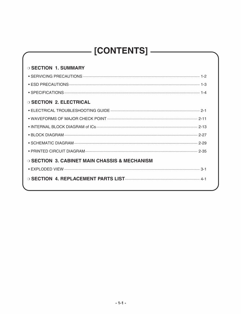
SECTION 1. SUMMARY
• SERVICING PRECAUTIONS .......................................................................................................... 1-2
• ESD PRECAUTIONS....................................................................................................................... 1-3
• SPECIFICATIONS........................................................................................................................... 1-4
SECTION 2. ELECTRICAL
• ELECTRICAL TROUBLESHOOTING GUIDE ................................................................................. 2-1
• WAVEFORMS OF MAJOR CHECK POINT .................................................................................. 2-11
• INTERNAL BLOCK DIAGRAM of ICs............................................................................................ 2-13
• BLOCK DIAGRAM......................................................................................................................... 2-27
• SCHEMATIC DIAGRAM................................................................................................................ 2-29
• PRINTED CIRCUIT DIAGRAM...................................................................................................... 2-35
SECTION 3. CABINET MAIN CHASSIS & MECHANISM
• EXPLODED VIEW ........................................................................................................................... 3-1
SECTION 4. REPLACEMENT PARTS LIST.................................................................... 4-1
[CONTENTS]
- 1-2 -
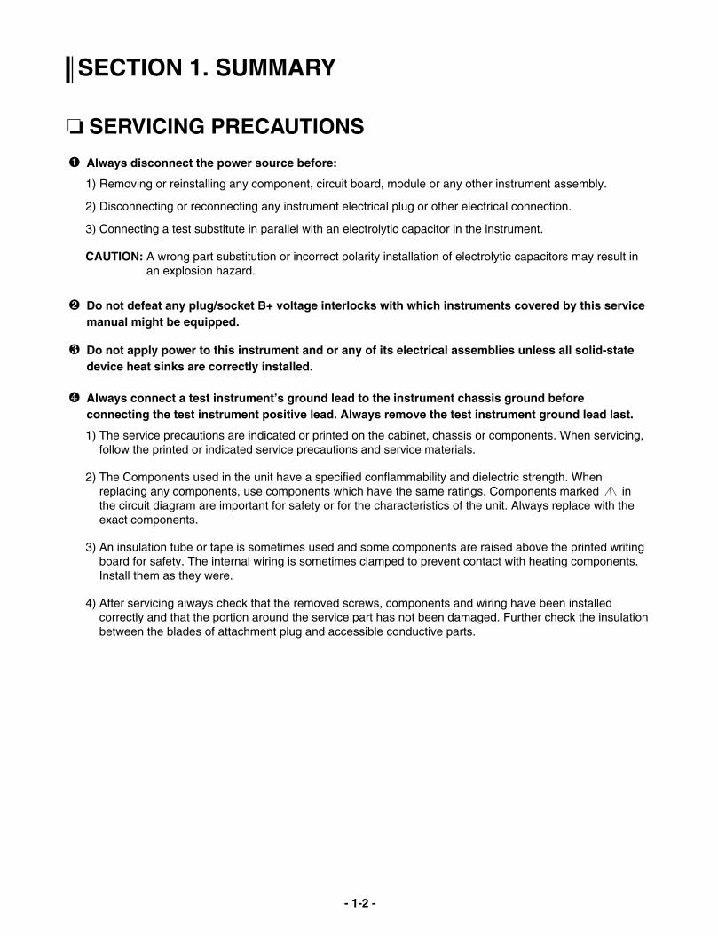
SERVICING PRECAUTIONS
Always disconnect the power source before:
1) Removing or reinstalling any component, circuit board, module or any other instrument assembly.
2) Disconnecting or reconnecting any instrument electrical plug or other electrical connection.
3) Connecting a test substitute in parallel with an electrolytic capacitor in the instrument.
CAUTION: A wrong part substitution or incorrect polarity installation of electrolytic capacitors may result inan explosion hazard.
Do not defeat any plug/socket B+ voltage interlocks with which instruments covered by this servicemanual might be equipped.
❸ Do not apply power to this instrument and or any of its electrical assemblies unless all solid-statedevice heat sinks are correctly installed.
❹ Always connect a test instrument’s ground lead to the instrument chassis ground beforeconnecting the test instrument positive lead. Always remove the test instrument ground lead last.
1) The service precautions are indicated or printed on the cabinet, chassis or components. When servicing,follow the printed or indicated service precautions and service materials.
2) The Components used in the unit have a specified conflammability and dielectric strength. Whenreplacing any components, use components which have the same ratings. Components marked inthe circuit diagram are important for safety or for the characteristics of the unit. Always replace with theexact components.
3) An insulation tube or tape is sometimes used and some components are raised above the printed writingboard for safety. The internal wiring is sometimes clamped to prevent contact with heating components.Install them as they were.
4) After servicing always check that the removed screws, components and wiring have been installedcorrectly and that the portion around the service part has not been damaged. Further check the insulationbetween the blades of attachment plug and accessible conductive parts.
SECTION 1. SUMMARY

- 1-3 -
ESD PRECAUTIONS
[Electrostatically Sensitive Devices (ESD)]Some semiconductor (solid state) devices can be damaged easily by static electricity. Such omponentscommonly are called Electrostatically Sensitive Devices (ESD). Examples of typical ESD devices areintegrated circuits and some field-effect transistors and semiconductor chip components. The followingtechniques should be used to help reduce the incidence of component damage caused by static electricity.
1) Immediately before handling any semiconductor component or semiconductor-equipped assembly, drainoff any electrostatic charge on your body by touching a known earth ground. Alternatively, obtain andwear a commercially available discharging wrist strap device, which should be removed for potentialshock reasons prior to applying power to the unit under test.
2) After removing an electrical assembly equipped with ESD devices, place the assembly on a conductivesurface such as aluminum foil, to prevent electrostatic charge buildup or exposure of the assembly.
3) Use only a grounded-tip soldering iron to solder or unsolder ESD devices.
4) Use only an anti-static solder removal device. Some solder removal devices not classified as “anti-static”can generate electrical charges sufficient to damage ESD devices.
5) Do not use freon-propelled chemicals. These can generate electrical charges sufficient to damage ESDdevices.
6) Do not remove a replacement ESD device from its protective package until immediately before you areready to install it. (Most replacement ESD devices are packaged with leads electrically shorted togetherby conductive foam, aluminum foil or comparable conductive material).
7) Immediately before removing the protective material from the leads of a replacement ESD device, touchthe protective material to the chassis or circuit assembly into which the device will be installed.
CAUTION: Be sure no power is applied to the chassis or circuit, and observe all other safety precautions.
8) Minimize bodily motions when handling unpackaged replacement ESD devices. (Otherwise harmlessmotion such as the brushing together of your clothes fabric or the lifting of your foot from a carpeted floorcan generate static electricity sufficient to damage an ESD device).
[CAUTION. GRAPHIC SYMBOLS]
THE LIGHTNING FLASH WITH APROWHEAD SYMBOL. WITHIN AN EQUILATERALTRIANGLE, IS INTENDED TO ALERT THE SERVICE PERSONNEL TO THE PRESENCEOF UNINSULATED “DANGEROUS VOLTAGE” THAT MAY BE OF SUFFICIENTMAGNITUDE TO CONSTITUTE A RISK OF ELECTRIC SHOCK.
THE EXCLAMATION POINT WITHIN AN EQUILATERAL TRIANGLE IS INTENDED TOALERT THE SERVICE PERSONNEL TO THE PRESENCE OF IMPORTANT SAFETYINFORMATION IN SERVICE LITERATURE.

- 1-4 -
1. GENERAL
Power requirements ..................................................................................................................... DC12V~15V
Ground system ................................................................................................................................... Negative
Dimensions(W x H x D) ...................................................................................................... 188 x 58 x 166mm
Weight .............................................................................................................................................. Net: 1.3kg
2. RADIO SECTION
FM AM(MW)Frequency range 65.0~74.0MHz(Optional), 522~1,620kHz
87.5~108MHz (Optional:530~1,710kHz/ 520~1,620kHz)
Intermediate frequency 10.8MHz 450kHz
Usable sensitivity 12dBµV 32dBµV
Signal to noise ratio 55dB 45dB
3. COMPACT DISC SECTION
Frequency response..................................................................................................................... 40Hz~20kHz
Channel separation ...................................................................................................................... 50dB(1kHz)Signal to noise ratio .................................................................................................................................. 70dB
4. AUDIO SECTION
Maximum output power ....................................................................................................................... 50W x 4
Speaker impedance ............................................................................................................... 4Ω x 4 or 8Ω x 4
NOTE: The design and specifications are subject to change without notice in the sourse of productimprovement.
SPECIFICATIONS
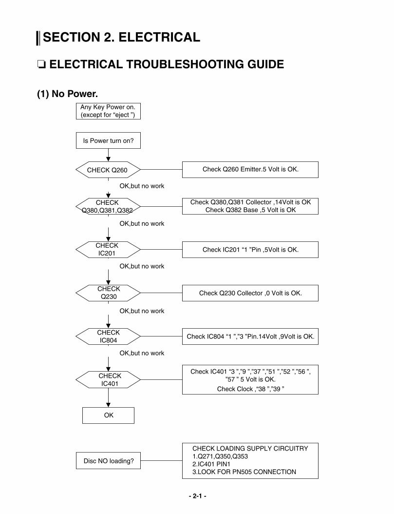
- 2-1 -
ELECTRICAL TROUBLESHOOTING GUIDE
Any Key Power on.(except for “eject ”)
Is Power turn on?
OK,but no work
OK,but no work
OK,but no work
OK,but no work
OK,but no work
Check Q260 Emitter.5 Volt is OK.
Check IC201 “1 ”Pin ,5Volt is OK.
Check Q230 Collector ,0 Volt is OK.
Check IC804 “1 ”,”3 ”Pin.14Volt ,9Volt is OK.
Check IC401 “3 ”,”9 ”,”37 ”,”51 ”,”52 ”,”56 ”,”57 ” 5 Volt is OK.
Check Clock ,“38 ”,”39 ”
CHECK LOADING SUPPLY CIRCUITRY1.Q271,Q350,Q3532.IC401 PIN13.LOOK FOR PN505 CONNECTION
Check Q380,Q381 Collector ,14Volt is OKCheck Q382 Base ,5 Volt is OK
CHECK Q260
CHECKQ380,Q381,Q382
CHECKIC201
CHECKQ230
CHECKIC804
CHECKIC401
OK
Disc NO loading?
(1) No Power.
SECTION 2. ELECTRICAL

- 2-2 -
YES
YES
YES
YES
YES
YES
(2) LCD light abnornal.
Any Key power on.(without DISC)
Do display LCD then light?Check voltage in the power supply
circuitry.Power supply circuitry defective.
Q371,Q372,IC403
• Reset circuit defective.IC201 Surrounding circuitdefective.
• IC401 pin89 defective.
X401, C415, C416.
Q260, PN401 frontPCB pattern defective.
IC401, Pin66, 67, 87front PCB pattern defective.
IC901, Surrounding circuitPCB pattern defective.
Is u-com IC401 reset circuitnormal? Pin88
Is u-com IC401 keyin Pin9, 37, 51,52, 64 5volt input?
Is u-com IC401 Pin 66,67,87output waveform normal?
Is IC901 Com1, Com2, Com3output waveform normal?
Display LCD connector defective.
Is u-com IC401X1, X2 terminalPin38,39input?OSC : 12.5MHz
NO NO
NO
NO
NO
NO
NO

- 2-3 -
(3) CD PART

- 2-4 -
"READING" DISPLAY CHECK (=ONLY "CD" DISPLAY)

- 2-5 -
READING OK CHECK (="NO DISC" DISPLAY)

- 2-6 -
READING OK CHECK #A (="NO DISC" DISPLAY)

- 2-7 -
READING OK CHECK #B (="NO DISC" DISPLAY)
- 2-8 -
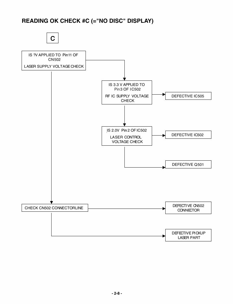
READING OK CHECK #C (="NO DISC" DISPLAY)

- 2-9 -
READING OK CHECK #D (="NO DISC" DISPLAY)

- 2-10 -
READING OK CHECK #E (="NO DISC" DISPLAY)

- 2-11 -
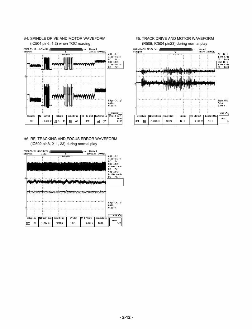
#1. MICOM INTERFACE WAVEFORM(CN503 1 9,2 1 ,1 8,20) during normal play
#2. SLED DRIVE AND MOTOR WAVEFORM(IC504 pin5, 1 4) when focus search
#3. FOCUS DRIVE AND MOTOR WAVEFORM(R5 1 3, IC504 pin 1 5)• When focus search failed or there is no disc on the
tray• There is disc on tray and focus search success
WAVEFORMS OF MAJOR CHECK POINT
- 2-12 -
#4. SPINDLE DRIVE AND MOTOR WAVEFORM(IC504 pin6, 1 2) when TOC reading
#5. TRACK DRIVE AND MOTOR WAVEFORM(R508, IC504 pin23) during normal play
#6. RF, TRACKING AND FOCUS ERROR WAVEFORM(IC502 pin8, 2 1 , 23) during normal play

- 2-13 -
IC401 PD784214A1) PORT ASSIGNMENT
INTERNAL BLOCK DIAGRAM of ICs
- 2-14 -
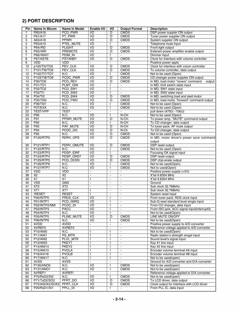
2) PORT DESCRIPTION
Pin Name In Micom Name In Model Enable I/O I/O Output Format Description1 P60/A16 PCD_PWR I/O O CMOS DSP power suppler ON output2 P61/A17 PT_PWR I/O O CMOS Tuner power supplier ON output3 A63/A18 PPWR I/O O CMOS System suppleir ON output4 P63/A19 PTEL_MUTE I/O I - Telephone mute input5 P64//RD PLIGHT I/O O CMOS Front light output6 P65//WR PREMOTE I/O O CMOS Exteranl power amplifier enable output7 P66//WAIT PDIM_IN I/O I - Dimmer input8 P67/ASTB PSTANBY I/O O CMOS Clock for interface with volume controller9 VDD VDD - - - Positive power spply10 p100/TI5/TO5 PEV_CLK I/O O CMOS Clock for interface with volum controller11 P101/TI6/TO6 PEV_CLK I/O O CMOS To volume controller, data output12 P102/TI7/TO7 N.C. I/O I CMOS Not to be used (Open)13 P103/TI8/TO8 PCDC_PWR I/O O CMOS CD changer power supplier ON output14 P30/TO0 PCD_REV I/O O CMOS In MD, load motor "revers" command output15 P31/TO1 PLMT_ISW I/O I - In MD, limit switch state input16 P32/TO2 PCD_SW1 I/O I - In MD, SW1 state input17 P33/TI1 PCD_SW2 I/O I - In MD, SW2 state input18 P34/TI2 PCD_SW4 I/O O CMOS In MD, switching load and sled motor19 P35/TI00 PCD_FWD I/O O CMOS In MD, load motor "forward" command output20 P36/TI01 N.C. I/O I CMOS Not to be used (Open)21 P37/EXA N.C. I/O I CMOS Not to be used (Open)22 TEST/VPP TEST - - - pull down (470Ω ~10kΩ)23 P90 N.C. I/O I N-CH Not to be used (Open)24 P91 PPWR_MUTE I/O O N-CH To power amp, "MUTE" command output25 P92 N.C. I/O I N-CH To CD changer, data output26 P93 PAF_MUTE I/O O N-CH To tuner pack, AF mute output27 P94 PCDC_DO I/O O N-Ch To CD changer, data output28 P95 N.C. I/O O CMOS Not to be used (Open)29 P120/RTP0 RDRV_OPS I/O O CMOS In MD, motor driver's power save command
output30 P121/RTP1 PDRV_OMUTE I/O O CMOS DSP reset output31 P122/RTP2 N.C. I/O I CMOS Not to be used (Open)32 P123/RTP3 PDSP_IDRF I/O I - Focusing OK signal input33 P124/RTP4 PDSP_ORST I/O O CMOS DSP reset output34 P125/RTP5 PCD_OCEN I/O O CMOS DSP chip enale output35 P126/RTP6 N.C. I/O I CMOS Not to be used(Open)36 P127/RTP7 N.C. I/O I CMOS Not to used(Open)37 VDD VDD - - - Positive power supply (+5V)38 X2 X2 - - - X’tal 9.8304 MHz39 X1 X1 I - - X’tal 9.8304 MHz40 VSS GND - - - Ground41 XT2 XT2 - - - Sub clock 32.768kHz42 XT1 XT1 I - - Sub clock 32.768kHz43 /RESET RESET I - - System reset input44 P00/INTP0 PRDS_CLK I/O I - From tuner pack, RDS clock input45 P01/INTP1 PCD_IWRQ I/O I - Sub-Q read standard level singla input46 P02/INTP2/NMI PCDC_DI I/O I - From CD changer, data input47 P03/INTP3 PACC I/O I - From ISO jack, ACC signal input(interrupt3)48 P04/INTP4 N.C. I/O I - Not to be used(Open)49 P05/INTP5 PLINE_MUTE I/O O CMOS LINE MUTE ON/OFF50 P06/INTP6 N.C. I/O I CMOS Not to be used(Open)51 AVDD AVDD - - - Positive power supply to A/D converter52 AVREF0 AVREF0 - - - Reference voltage applied to A/D converter53 P10/ANI0 N.C. I I - Not to be used(Open)54 P11/ANI1 PS_MTR I I - Radio station’s strength singal input55 P12/ANI2 PLVL_MTR I I - Sound level’s signal input56 P13/ANI3 PKEY1 I I - Key #1 line input57 P14/ANI14 PKEY2 I I - Key #2 line input58 P15/ANI15 PVOLA I I - Encoder volume terminal #A input59 P16/AVI16 PVOLB I I - Encoder volume terminal #B input60 P17/ANI17 N.C. I I - Not to be used(open)61 AVSS AVSS - - - Ground for A/D converter and D/A converter62 P130/ANO0 N.C. I/O I CMOS Not to be used(open)63 P131/ANO1 N.C. I/O I CMOS Not to be used(open)64 AVREF1 AVREFI - - - Reference voltage applied to D/A converter65 P70/RxD2/SI2 N.C. I/O I CMOS Not to be used(open)66 P71/TxD2/SO2 PFRT_DO I/O O CMOS To LCD driver, data output67 P72/ASCK2/SCK2 PFRT_CLK I/O O CMOS Clock output for interface with LCD driver68 P20/RxD1/SI1 PPLL_DI I/O I - From PLL IC, data input

- 2-15 -
Pin Name In Micom Name In Model Enable I/O I/O Output Format Description69 P21/TxD1/SO1 PPLL_DO I/O O CMOS To PLL IC, data output70 P22/ASCK1/SCK1 PPLL_CLK I/O O CMOS Clcok output for inpterface with PLL IC71 P23/PCL PPLL_CE I/O O CMOS PLL IC enable output72 P24/BUZ PBEEP I/O O CMOS Beep sound output (2kHz)73 P25/SI0/SDA0 PDSP_IDA I/O I - From DSP, data input74 P26/SO0 PDSP_ODA I/O O CMOS To DSP, data output75 P27//SCKO/SCLO PDSP_OCLK I/O O CMOS Not to be used (Open)76 P80/A0 N.C. I/O I CMOS Not to be used (Open)77 P81/A1 N.C. I/O I CMOS Not to be used (Open)78 P82/A2 N.C. I/O I CMOS Not to be used (Open)79 P83/A3 PST I/O I - Stereo indigater's signal or SD signal input80 P84/A4 PRDS_DI I/O I - From tuner pack, RDS data input81 P85/A5 POPT_IN0 I/O I - For diode option check, signal 1 or 2 input082 P86/A6 POPT_IN1 I/O I - For diode option check, signal 1 or 2 input183 P87/A7 POPT_IN2 I/O I - For diode option check, signal 1 or 2 input284 P40/AD0 POPT_OUTO I/O O CMOS For dinde option check, signal 1 output85 P41/AD1 POPT_OUT1 I/O O CMOS For dinde option check, signal 1 output86 P42/AD2 N.C. I/O I - Not to be used (Open)87 P43/AD3 PFRT_CE I/O O CMOS LCD driver enable output88 P44/AD4 PFRT_RES I/O O CMOS LCD driver reset output89 P45/AD5 N.C. I/O I - Not to be used (Open)90 P46/AD6 PANT I/O O CMOS Antenna control output91 P47/AD7 N.C. I/O I - Not to be used (Open)92 P50/A8 N.C. I/O I CMOS Not to be used (Open)93 P51/A9 PVOL_MUTE I/O O CMOS Direct volume mute signal output94 P52/A10 N.C. I/O I CMOS Not to be used (Open)95 P53/A11 N.C. I/O I CMOS Not to be used (Open)96 P54/A12 N.C. I/O I CMOS Not to be used (Open)97 P55/A13 N.C. I/O I CMOS Not to be used (Open)98 P56/A14 N.C. I/O I CMOS Not to be used (Open)99 P57/A15 N.C. I/O I CMOS Not to be used (Open)100 VSS VSS - - - Ground
input port setted 23output port setted 34Used I/O port 57Interrupt 4A/D Converter 4

- 2-16 -
IC501 MN6627933CG

- 2-17 -
1) BLOCK DIAGRAM

- 2-18 -
Pin No. Symbol I/O Function1 D11 I/O DRAM data signal I/O 112 D10 I/O DRAM data signal I/O 103 D9 I/O DRAM data signal I/O 94 D8 I/O DRAM data signal I/O 85 UDQM O SDRAM upper byte data mask signal output6 SDRCK O SDRAM clock signal output7 A11 O DRAM address signal output 118 A9 O DRAM address signal output 99 A8 O DRAM address signal output 810 A7 O DRAM address signal output 711 A6 O DRAM address signal output 612 A5 O DRAM address signal output 513 A4 O DRAM address signal output 414 LDQM O SDRAM lower byte data mask signal output15 NWE O DRAM write enable signal output16 NCAS O DRAM CAS control signal output17 NRAS O DRAM RAS control signal output18 NCS O SDRAM chip select signal output19 A3 O DRAM address signal output 320 A2 O DRAM address signal output 221 A1 O DRAM address signal output 122 A0 O DRAM address signal output 023 DRVDD1 I Power supply 1 for DRAM interface I/O24 DVSS1 I Ground 1 for digital circuits25 A10 O DRAM address signal output 1026 *BA1 O SDRAM bank selection signal output 127 *BA0 O SDRAM bank selection signal output 028 DVDD1 I Power supply 1 for internal digital circuits29 SPOUT O Spindle drive signal output (absolute value)30 *SPPOL O Spindle drive signal output (polarity)31 TRVP O Traverse drive signal output (positive polarity)32 *TRVM O Traverse drive signal output (negative polarity)33 *TRVP2 O Traverse drive signal output 2 (positive polarity)34 *TRVM2 O Traverse drive signal output 2 (negative polarity)35 TRP O Tracking drive signal output (positive polarity)36 *TRM O Tracking drive signal output (negative polarity)37 FOP O Focus drive signal output (positive polarity)38 *FOM O Focus drive signal output (negative polarity)39 IOVDD1 I Power supply 1 for digital I/O40 TBAL O Tracking balance adjustment signal output41 FBAL O Focus balance adjustment signal output42 FE I Focus error signal input43 TE I Tracking error signal input44 ADPVCC I Voltage input for supply voltage monitor45 RFENV I RF envelope signal input46 LDON O Laser ON signal output47 NRFDET I RF detectoion signal input48 OFT I Off-track signal input49 BDO I Dropout signal input50 AVDD1 I Power supply 1 for analog circuits51 IREF I Analog reference current input52 ARF I RF signal input53 DSLF O DSL loop filter pin54 PWMSEL I PWM output mode selection input Low: Direct High: 3-state55 PLLF O PLL loop filter pin (for phase comparison)56 PLLFO O PLL loop filter pin (for speed comparison)57 AVSS1 I Ground 1 for analog circuits58 LOOUTL O L-ch audio output for line-out output59 LOVSS1 I Ground for line-out output
3) PORT DESCRIPTION

- 2-19 -
Pin No. Symbol I/O Function60 LOOUTR O R-ch audio output for line-out output61 LOVDD1 I Power supply for line-out output62 N.C. - -63 TMON1 O Test monitor output 164 N.C. - -65 N.C. - -66 TMON2 O Test monitor output 267 DVDD3 I Power supply 3 for digital circuits68 DVSS2 I Ground 2 for digital circuits69 *EXT0 I/O Expansion I/O port 070 *EXT1 I/O Expansion I/O port 171 *EXT2 I/O Expansion I/O port 272 MCLK I Microcontroller command clock signal input73 MDATA I Microcontroller command data signal input74 MLD I Microcontroller command load signal input75 *STAT O Status signal output76 *BLKCK O Subcode block clock signal output77 *SMCK O 4.2336-/8.4672-MHz clock signal output78 *PMCK O 88.2-kHz clock signal output79 *TX O Digital audio interface signal output80 *FLAG O Flag signal output81 NRST I LSI reset signal input82 NTEST I Test mode setting input83 DVSS3 I Ground 3 for digital circuits84 X1 I Crystal oscillator circuit input85 X2 O Crystal oscillator circuit output86 IOVDD2 I Power supply 2 for digital I/O87 DVDD2 I Power supply 2 for internal digital circuits88 D2 I/O DRAM data signal I/O 289 D1 I/O DRAM data signal I/O 190 D0 I/O DRAM data signal I/O 091 D3 I/O DRAM data signal I/O 392 D4 I/O DRAM data signal I/O 493 D5 I/O DRAM data signal I/O 594 D6 I/O DRAM data signal I/O 695 D7 I/O DRAM data signal I/O 796 D15 I/O DRAM data signal I/O 1597 D14 I/O DRAM data signal I/O 1498 DRVDD2 I Power supply 2 for DRAM interface I/O99 D13 I/O DRAM data signal I/O 13100 D12 I/O DRAM data signal I/O 12
- 2-20 -
CLK
ADD
LCKE
LRAS LCBR LWE
CLK CKE CS RAS CAS WE L(U)DQM
LDQMLWCBRLCAS
Bank Select
LWE
LDQM
DQI
Data Input Regidter
512K x 16
512K x 16
Column Decoder
Latency & Burst Length
Programming Register
Timing Register
Address R
egister
Row
Decoder
LCB
R
LRA
S
Sense A
MP
I/O C
ontrolO
utput Buffer
Col. B
uffer
Row
Buffer
Refresh C
ounter
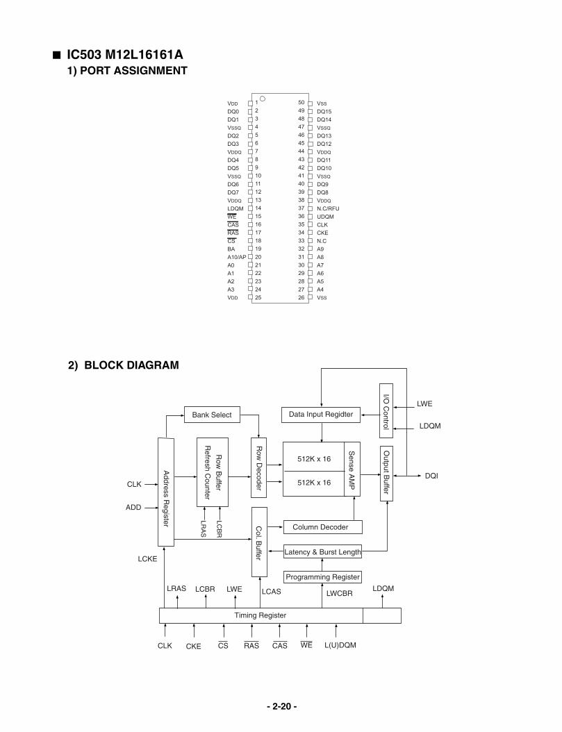
IC503 M12L16161A1) PORT ASSIGNMENT
2) BLOCK DIAGRAM

- 2-21 -
Pin Name Input FunctionCLK System Clock Active on the positive going edge to sample all inputs.
CS Chip Select Disables or enables device operation by masking or enabling all inputs except CLK, CKE and L(U)DQM.Masks system clock to freeze operation from the next clock cycle. CKE
CKE Clock Enable should be enabled at least one cycle prior to new command. Disable input buffers for power down in standby.
A0~A10/AP Address Row/Column addresses are multiplexed on the same pins. Row address: RA0~RA10, column address: CA0~CA7
BA Bank Select Address Selects bank to be activated during row address latch time. Selects bank for read/write during column address latch time.
RAS Row Address Strobe Latches row addresses on the positive going edge of the CLK with RAS low. Enables row access & precharge.
CAS Column Address Strobe Latches column addresses on the positive going edge of the CLK with CAS low. Enables column access.
WE Write Enable Enables write operation and row precharge. Latches data in starting from CAS, WE active.
L(U)DQM Data Input / Output Mask Makes data output Hi-Z, tSHZ after the clock and masks the output. Blocks data input when L(U)DQM active.
DQ0~15 Data Input / Output Data inputs/outputs are multiplexed on the same pins.VDD/VSS Power Supply/Ground Power and ground for the input buffers and the core logic.
VDDQ/VSSQ Data Output Power/Ground Isolated power supply and ground for the output buffers to provide improved noise immunity.
N.C/RFU No Connection/ This is recommended to be left No Connection on the Reserved for Future Use device.
28 27 26 25 24 23 22 21 20 19 18 17 16 15
1 2 3 4 5 6 7 8 9 10 11 12 13 14
+
+
— + —
+—
+—
+—
7.5k
7.5k
7.5k
7.5k
LOADING PREFWE REV
X3POWER
SAVE
16k
16k
16k
16k
PREVCC(PRE. LODING)
PREVCC12(CH1. CH2)
CD1~ CB4MUTE
POWVCC34(CH3, CH4)
10k
10k
10k 10k
10k10k
10k
10k
LEVELSHIFT
LEVELSHIFT
LEVELSHIFT
LEVELSHIFT
10k
10k
10k
10k10k
10k
3) PIN FUNCTION TABLE
IC504 BA5810FM

- 2-22 -
IC505 AMC1117
1) BLOCK DIAGRAM

- 2-23 -
IC601TDA7348D

- 2-24 -
IC801 TB2903HQ

- 2-25 -
IC901 PT65241) BLOCK DIAGRAM
2) PIN CONFIGURATION

- 2-26 -

2-27 2-28
BLOCK DIAGRAM

2-29 2-30
SCHEMATIC DIAGRAM 1. MAIN SCHEMATIC DIAGRAM

2-31 2-32
2. FRONT SCHEMATIC DIAGRAM
2-33 2-34
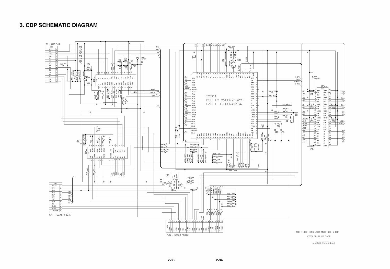
3. CDP SCHEMATIC DIAGRAM

2-35 2-36
PRINTED CIRCUIT DIAGRAM
1. MAIN P.C. BOARD

2-37 2-38
2. FRONT P.C. BOARD

2-39 2-40
2. FRONT P.C. BOARD

2-41 2-42
3. CDP P.C. BOARD (TOP) 3. CDP P.C. BOARD (BOTTOM)

2-43 2-44
5. LED P.C.BOARD (BOTTOM)
5. LED P.C.BOARD (TOP)4. TRIM P.C. BOARD (BOTTOM)4. TRIM P.C. BOARD (TOP)

3-1 3-2
EXPLODED VIEW
283
284286
285
281
282
A43279
278
A45
A42
452
253
252
251
276
287
272
271
270
269
262
258
257
261
260
259288
268
267
266
265
264
277
273
255
256
274
275
254
453
A46
A41
280
A26
450
451
250
A44
NOTE) Refer to “SECTION 4 REPLACEMENTPARTS LIST” in order to look for the part number of each part.
SECTION 3. CABINET MAINCHASSIS & MECHANISM


![KD DB97BT E - · PDF filedeutsch b5a-0817-00 [e] kd-db97bt cd receiver ... rÉcepteur cd manuel d’instructions cd-receiver bedienungsanleitung js_jvc_kd_db97bt_e_c_00.indd 1 12/11/2015](https://img.pdfslide.us/doc/110x75/5a7cc20f7f8b9a66798d12a6/kd-db97bt-e-b5a-0817-00-e-kd-db97bt-cd-receiver-rcepteur-cd-manuel-dinstructions.jpg)


![CD RECEIVER KD-SH99 - JVCresources.jvc.com/Resources/00/00/98/LVT0654-001A.pdf · ENGLISH LVT0654-001A [J] ESPAÑOL FRANÇAIS CD RECEIVER KD-SH99 RECEPTOR CON CD KD-SH99 RECEPTEUR](https://img.pdfslide.us/doc/110x75/6016df5fdaebda50c95a75b2/cd-receiver-kd-sh99-english-lvt0654-001a-j-espaol-franais-cd-receiver-kd-sh99.jpg)