Embed Size (px)
Citation preview

Capacitor Only SVC Voltage Control Algorithm
EE5200 Term Project
Instructor: Dr. Bruce Mork
Team Members:
Kevin Thompson and John Leicht
Fall 2011

Executive Summary
In addition to the research and experimentation need to understand the basic control
features of an SVC, much effort was also expended on learning the Matlab simulation
software. While the Matlab SimPowerSystems and Simulink libraries contain many easily
recognizable built-in control blocks, learning how each block worked required careful
study and much experimentation. Even the simple “scope” Simulink block required
experimentation to affectively use this tool that was needed to develop our controller.
Unfamiliarity with the Matlab simulation software coupled with minimal understanding
of SVC control methods resulted in various, and sometimes unnecessarily intricate,
versions of our TSC only SVC controller. Our final version surprisingly mimics the
published examples of SVC controllers consisting of a voltage control block feeding into
a TSC selector block.
For our version of an SVC controller, the user selectable parameters were entered at the
voltage control block and consisted of a reference voltage, and desired bandwidth.
Given the actual bus voltage, the voltage control block outputs a Q required signal
which is fed into our “B-selector” block. The B-selector activates or deactivates the
individual TSC branches based on the Q required. To test the controller, a basic primary
system was designed consisting of a 3-phase voltage source and 3-phase dynamic
load. The voltage source and associated parameters were selected to represent a
major transmission node with many connected transmission paths and no local
generation available for voltage control. The loading of the bus was simulated using a
dynamic load model. A dynamic load model was selected to better mimic real world
system load. Unlike a static RL load, a dynamic load can be configured to mimic the
constant power demands of induction machines. To this basic system was added fixed
resistors which were energized using time controlled CB’s. The CB’s were timed to turn
on the associated loads at somewhat variable time increments to study the response of
the SVC controller to changes in the bus voltage. In summary, the control system
needed to turn on and off the TSC branches are simple but effective. In our testing, two
basic system conditions were used, strong and weak, to expose our controller design to
varying conditions. Without the SVC, the bus voltage dipped to as low as 82% when
exposed to our test conditions but never dipped below 95% or above 103% with the
SVC controller active.

Table of contents
1 Introduction
1.1 Introduce SVC concept
2 Background
3 Proposed Approach
3.1 Develop balanced 3-phase system model
3.1.1 Generator as source model
3.1.2 Dynamic load model
3.2 Define SVC characteristics
3.3 Develop control algorithm
3.3.1 Voltage filter block
3.3.2 Voltage control block
3.3.3 B-selector block
3.3.4 Oscillation damper block
3.4 Develop test method
4 Simulation of test scenarios
5 Results
6 Conclusions
7 Recommendations for Continued Work
Statement of Contribution
This was a collaborative effort from both team members with first draft responsibility of
individual sections of the report split equally between team members. The Matlab
SimPowerSystem file development was a collaborative effort as well including the
Simulink control blocks and test case parameters.
1 Introduction
Static Var Compensators (SVCs) are used in power systems for voltage control. The
basic purpose of a SVC is to rapidly supply or absorb Vars from the system during system
events that would otherwise result in unacceptable over or under voltage conditions
[1,2,3]. The basic component of a SVC which makes rapid response of a SVC possible is
the use of thyristor based switches. The thyristor switches essentially close and open
within a very short time period when compared to mechanical switches [1]. When
coupled with the appropriate control circuit the thyristor switches can connect either

shunt capacitive or inductive load onto the system as needed [2]. Our Term Project will
attempt to develop a control system for a capacitor only SVC. The system modeled will
be assumed to not suffer from over voltage conditions and therefore a SVC which can
absorb Vars is not needed.
1.1 Introduce SVC concept
Static VAR compensators (SVCs) are devices which use reactors and/or capacitors
coupled with thyristor switches to control voltage or reactive power. One SVC may
contain multiple capacitor units and multiple reactor units connected in shunt through
a step-up transformer. Each capacitor unit or reactor unit are switched using thyristors.
The thyristor can be ON/OFF type or use phase angle control with reactors to give
variable ON time, providing variable reactive power [1].
SVCs are available in several combinations of the aforementioned configurations. The
ON/OFF switched capacitor unit is referred to as thyristor switched capacitor (TSC). The
ON/OFF switched reactor unit is referred to as thyristor switched reactor (TSR). The
phase angle controlled reactor is referred to as thyristor controlled reactor (TCR). TCRs
require additional series capacitance to filter harmonics created due to the phase
angle control [2]. Each of these units can be combined to create an appropriate SVC
device.
SVCs provide fast and variable VAR control relative to fixed shunt capacitors and
reactors. Thyristor control gives the SVC almost immediate response. The SVC is also
allowed to switch much more frequently because it uses thyristors instead of circuit
breakers or other mechanical switching device. Also, using TSC with TCR allows almost
infinitely variable VAR flow from its maximum VAR production to maximum VAR
absorption [1].
SVCs can be used to control voltage and VAR flow. Due to their fast and variable
nature, SVCs are capable of providing voltage support during system disturbances. This
voltage support may prevent approaching the stability limits of nearby generators. It

may also be used to control voltage following the switching in or out of lines and other
system components.
2 Background
The goal of this project is to define a controlling algorithm which applies and removes
VARs in response to changing voltage conditions. For simplicity only TSCs will be
considered. The idea is that a SVC is installed at a bus to support the voltage following
system events which lower bus voltage. With each change in the system load and
each change in the system topology, the bus voltage changes. The SVC should
respond by switching capacitive loads to maintain the bus voltage within acceptable
limits.
The project will define system parameters for both strong and weak systems. The strong
system is defined as having a large short circuit current and small system source
impedance. The weak system is defined as having a small short circuit current and
large system source impedance. The control algorithm must be capable of adapting
to either extreme.
The project will also define and simulate dynamic system events which change the bus
voltage. These system events could be adding or removing large loads, switching in or
out primary system components, or any other system change which will cause the bus
voltage to stray. The control algorithm must be capable of accommodating all
foreseeable system events and conditions.
The project will also define a SVC model which consists of TSC units, designed to control
the voltage at a given bus. The SVC model will use four TSC units capable of being
switched in 75MVAR increments. The TSCs will be switched on to boost the bus voltage
and switched off as the bus voltage recovers. The control algorithm presented will be
capable of maintaining the bus voltage within acceptable limits.

Matlab SimPowerSystems was chosen to model the power system for this project. This
software package provides multiple predefined power system building blocks which
ensure accurate system modeling and an intuitive system design.
3 Proposed Approach
The SVC in our project will be programmed to support the voltage at a single bus in the
power system. This means the entire system can be simplified around the selected bus
to be controlled. The power system model consists of a thevenin source connected to
a load at the bus of interest. Additional load is connected in parallel with the original
load to simulate system load level changes. The SVC consisting of shunt TSCs is also
connected in parallel with the loads. This model allows simulations for all applicable
system parameters to adequately test the viability of the control algorithm.
3.1 Develop balanced 3-phase system model
3.1.1 Generator as source model
Figure 1: Source Model [11]

The thevenin equivalent source is modeled as a three phase source with series
resistance and inductance [11]. The series resistance and inductance represent the
source impedance of the power system at the selected bus. The strength of the system
is inversely proportional to the size of resistance and reactance in the source
impedance. For example, larger source impedances reflect a weaker system. These
values are set by selecting the X/R ratio and available fault value measured in volt-
amps.
3.1.2 Dynamic load model
Figure 2: Dynamic Load Model [11]
The initial system load is modeled as a three phase dynamic load. The real and
reactive power in the dynamic load changes as a function of the voltage change from
nominal. The SimPowerSystems Matlab Dynamic Load is modeled using the following
equations:

P 1 P o
V1
Vo
n α.
. Q 1 Q o
V 1
V o
n β.
.References 5,6, and 11
The relationship between power the draw by a dynamic load versus the applied
voltage is an adjustable based on the values of the alpha and beta exponents chosen.
A constant current source can be modeled by selecting “np” and “nq” equal to “1”
[5]. These power values can also be used to simulate constant impedance by setting
“np” and “nq” equal to “2”. The effect of the value of the exponent on the power-
voltage relationship is easy to see apparent when the change in power across a resistor
is viewed as a function of voltage. The power drawn by the resistor can be seen to be
a function of the voltage squared:
P 1
V 12
RP 1
V 1
V o
V o.
2
RP 1 P o
V 1
V o
2
.
A constant power load is modeled when the exponents are set to 0. In a real system
the load would be a mix of all three types of loads with the actual exponents used
dependent on the expected load [6] Using a dynamic load allows the simulation to
more accurately demonstrate the effects in a real power system. Reference [6] lists
typical values for commercial, industrial and residential loads. Values of 1.3 were
chosen for alpha and 3.5 for Beta based on the typical values listed in the Appendix of
reference 6.
3.2 Define SVC characteristics
The SVC being used for this project consists of four TSC branches connected in shunt to
the system bus. The SVC is chosen as capacitive only without an inductive branch,

either TSR or TCR. The TSC units are modeled as three phase parallel RLC loads in series
with three phase breakers. The three phase parallel RLC loads are constant
impedance devices. The SVC TSC units are almost entirely capacitive in nature so only
the capacitive load value is entered. This load value is given in terms of capacitive
power absorbed at nominal voltage. The three phase breaker models the thyristor
switch in the TSC. This breaker is set to be controlled externally by the SVC voltage
control algorithm.
Example calculations of capacitive reactive compensation are below which are taken
from an example simulation in SimPowerSystems. The three phase source VA is 2500
MVA at 1.0 per unit voltage. The source X/R ratio is 10. The nominal voltage is 138kV.
Equation [1] calculates the magnitude of thevenin impedance per the source VA.
Zth = [ V / sqrt( 3 ) ]2 / ( VA / 3 ) [1]
Zth = [ 138000 / sqrt( 3 ) ]2 / ( 2500000000 / 3 )
Zth = 7.6176
Equations [2] and [3] calculate the complex values of thevenin impedance.
Xth = Zth * sin( tan-1( X/R ) ) [2]
Xth = 7.6176 * sin( tan-1( 10 ) )
Xth = 7.5798
Rth = Zth * cos( tan-1( X/R ) ) [3]
Rth = 7.6176 * cos( tan-1( 10 ) )
Rth = 0.7580

Equation [4] calculates the actual capacitive impedance required to boost the
voltage. Vk is the desired voltage value at the bus. Typically this is +/- 5% of nominal.
Vth is the initial voltage at the thevenin bus. Zth is the complex source impedance
which is determined in Equations [1], [2], and [3] above.
Vk = abs( Vth * -jXc / ( -jXc + Zth ) ) [4]
Vk2 = abs( Vth * -jXc / ( -jXc + Zth ) )2
0.952 = abs( 0.832 * -jXc / ( -jXc + 0.7580 + j7.5798) )2
Xc = 60.98
From Equation [4], use Equation [5] to calculate the MVAR rating of a capacitor bank
required to boost the desired thevenin bus voltage. For the given example it is
calculated that over 300 MVARs are required to boost this example bus voltage from
83.2% to 95%.
CAPMVAR = 3 * [ V / sqrt( 3 ) ]2 / Xc [5]
CAPMVAR = 3 * [ 138000 / sqrt( 3 ) ]2 / 60.98
CAPMVAR = 312.3 MVAR
The SVC system overall is a 675MVAR reactive compensation device. The TSC units are
each 75MVAR, 150MVAR, 150MVAR, and 300MVAR. With this combination of MVAR
sizes, any value of capacitive reactive compensation from 0 to 675MVAR can be
achieved in step sizes of 75MVAR.

3.3 Develop Control Algorithm
Based on reference [2] the basic SVC controller uses a voltage bandwidth, PID
controller, and Q selector circuit to control the reactive components of a SVC. While
the primary system components were modeled using the SimPowerSystems, the control
blocks were all done in Simulink. The various control portions were partitioned in two
basic control blocks and two support blocks: Voltage Filter block, Voltage Control
block, B-Selector block, and a Oscillation Damper block.
3.3.1 Voltage Filter Block
Figure 3: Voltage Filter
The Signal Filter block is shown in Figure 4 The Signal Filter block conditions the raw bus
voltage using a low pass filter with a time constant of 0.5 seconds. The low pass filter
eliminates the noise of the bus voltage signal. The need for filtering of the bus voltage
was mentioned in the reference [1] but the particulars behind the filter design were not
provided. Since steady-state response of the controller is all that is required, a low-pass
filter with a time-constant of 0.5 seconds was adequate to smooth out the signal. In
addition to the low pass filter, the voltage signal was converted to percent. With
Matlab, the unconditioned output signal from the built-in voltage measurement block
provides the magnitude of the voltage. Therefore to change the voltage into per unit
on a 138 kV base, the voltage was divided by (138,000*1.414)/1.732 or 112677 V.

3.3.2 Voltage Control Block
Figure 4: Voltage Control
The voltage control block shown in figure 5 changes the difference between the
measured bus voltage and the reference point into a Q required signal. Besides the
filtered bus voltage signal from the Signal Filter Block, the reference voltage or the
desired nominal % voltage is entered into the Voltage Control Block along with the
upper and lower bandwidth in %. Within the Voltage Control Block, the reference
voltage is subtracted from the filtered bus voltage signal resulting in a error signal. The
error signal is negative when the bus voltage is less than the reference voltage. For
example, with a nominal setting of 100%, if the actual measured bus voltage is at 96.9%,
the error signal would be a minus 0.1%. The error signal is then passed through a
Simulink block “Dead Zone Dynamic” [ 11]. The Dead Zone Dynamic uses the entered
upper and lower bandwidth to limit the response of the voltage controller to cases
when the voltage either rises above or drops below the window formed by the upper
and lower bandwidth. In the example case were the error signal is a minus 96.9%, the
output of the Dead Zone Dynamic would be a minus 0.1%. This value is fed into a
Simulink PID controller.

Figure 5: PID Control [11]
The PID controller proportional constant is set at 100, the integral constant is set at 300
and the derivative constant is set at zero. A controller form setting of Idea was chosen.
According the Simulink help windows, the Idea controller form of PID control multiplies
the integral component by the integral constant and then adds this result by one and
multiplies the sum by the proportional constant [11]. For example, if the generated
minus 0.1% remained for 1 second, the output of the PID controller would be -
100*(1+*1*0.1*300) or -130. The output of the PID controller continues to drop until the
voltage input to the Dead Zone Dynamic becomes zero. The output of the Dead Zone
Dynamic will become zero when the measured voltage signal is within the bandwidth
window. At this point the final value of output signal remains constant. In the above
example, if the PID output of -130 resulted in a TSC turning on and the bus voltage rose
to 98%, the input to the controller would remain at -130. The integral portion of the PID
controller is necessary to have a sustained output from the PID following the value of
the bus voltage returning to within the bandwidth window. A sustained output is
needed for correct operation of the next downstream control block in our SVC
controller. Two features available in the Simulink PID controller that control the falling
output of the PID controller are an “anti-windup method” [11] setting of “clamping”
and upper and lower saturation limits set at 700 and -700 respectively. The anti-windup

method of clamping stops the output of the PID from falling indefinitely by limiting the
PID output to the selected saturation limits. Without the PID output clamped, however,
the integral portion of the PID would continue to decrease, for the case of a negative
error signal, even past the saturation limits (though the actual output would not exceed
-700). Following a change in the bus voltage from below the bandwidth to above the
bandwidth the PID controller would have to unwind after the error signal reversed. If
allowed, winding up and down of the PID controller would result in an unnecessary
delay in response of the PID signal output and the downstream control blocks. The
saturation limits of 700 were selected to match the MVAR output of the total Capacitive
Mvar available from the SVC. The actual values chosen for the proportional and
integral constants are not relay important in our study since transient response of the
controller in not being studied. The necessary signal output would be reached
eventually even if smaller values were used but then a longer simulation time may be
needed. The final component of the Voltage Control Block is a gain of minus 1.
Inverting the output signal of the PID controller was necessary since the B-Selector
requires a positive value for the Q required
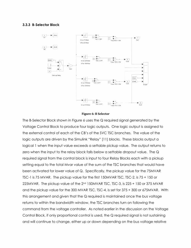
3.3.3 B-Selector Block
Figure 6: B Selector
The B-Selector Block shown in Figure 6 uses the Q required signal generated by the
Voltage Control Block to produce four logic outputs. One logic output is assigned to
the external control of each of the CB’s of the SVC TSC branches. The value of the
logic outputs are driven by the Simulink “Relay” [11] blocks. These blocks output a
logical 1 when the input value exceeds a settable pickup value. The output returns to
zero when the input to the relay block falls below a settable dropout value. The Q
required signal from the control block is input to four Relay Blocks each with a pickup
setting equal to the total Mvar value of the sum of the TSC branches that would have
been activated for lower value of Q. Specifically, the pickup value for the 75MVAR
TSC-1 is 75 MVAR. The pickup value for the first 150MVAR TSC, TSC-2, is 75 + 150 or
225MVAR. The pickup value of the 2nd 150MVAR TSC, TSC-3, is 225 + 150 or 375 MVAR
and the pickup value for the 300 MVAR TSC, TSC-4, is set for 375 + 300 or 675MVAR. With
this arrangement and given that the Q required is maintained once the bus voltage
returns to within the bandwidth window, the TSC branches turn on following the
command from the voltage controller. As noted earlier in the discussion on the Voltage
Control Block, if only proportional control is used, the Q required signal is not sustaining
and will continue to change, either up or down depending on the bus voltage relative

to the bandwidth window. This oscillation in the Q required signal would then result in
the oscillation of the relay output logic signals and the corresponding on and off again
oscillation of the TSC branches. With the integrating characteristic of the PID controller,
the output value from the PID will remain at whatever value was reached prior to the
bus voltage returning to within the bandwidth. For example, if the Voltage Control
Block began to produce a Q-required signal because the bus voltage was below the
bandwidth, the signal would integrate up until the Q-required signal became 75 MVAR.
At this point, the Relay block associated with TSC-1 would output a logical 1 and the
75MVARs of TSC-1 would be added in shunt to the bus. This action may raise the bus
voltage to above the lower bandwidth at which time the output of the PID would hold
a value slightly higher the 75 MVAR. If the bus voltage rises to above the upper
bandwidth, the Q-required signal would began to lower until the dropout setting of 60
MVAR of the TSC-1 Relay Block was reached and the TSC_1 CB would open. It is
possible that under some system conditions and voltage changes, the controller Q-
required value may oscillate between above 75 MVAR and Below 60 MVAR. This would
be an undesirable condition since the bus voltage would flicker up and down at the
rate equal to the on and off time constant of the SVC controller. To detect this
condition, an ancillary control block, Oscillation Damper Block, was developed to
detect this condition and take corrective action.
3.3.4 Oscillation Damper Block
Figure 7: Oscillation Damper

The oscillation Damper Block shown in Figure 7 detects possible on and off again
oscillation of the control signal for the 75 MVAR TSC_1 branch. This circuit uses two
Simulink Pulse Generators, a Sample and Hold block, a Counters block, and a Hold
Timer Block to identify the oscillation condition and drive the upper bandwidth to 110%
for 6 seconds. The expectation is that the resulting delta change in voltage associated
with the oscillations is less than the lower bandwidth plus 10%; therefore, with the
increase in the upper bandwidth, the TSC-1 branch will stay on and the system will be
stable for at least 6 seconds. A value of 6 seconds was chosen based on the arbitrarily
selected simulation time of 30 seconds and the arbitrary 5 second interval between
load changes. In the real world, if such oscillations actually occurred, a longer time
delay would most likely be used and an alarm would be sent to the designated
authority for corrective action. The Oscillation Damper Block only senses oscillations of
the 75 MVAR TSC branch. The reasoning for only monitoring the logic signal of TSC-1 is
based on the belief that the oscillations, if present, will always include the smaller
branch. Hence, only the smallest branch needs to be monitored.
The circuit works by holding the value of the TSC-1 logic signal for a fraction of second
and comparing the held signal value with the present signal value. The two signals are
compared using an exclusive OR logic gate, XOR If the TSC is either on or off
continuously, the output of the XOR will be 0 because the signal is not changing with
time. If, however, the logic signal is oscillating between 0 and 1, the rising and falling
edges of the TSC logic signal will be captured by the XOR and a signal sent to the
counter. The counter counts from 0 to 255 and then resets back to 0. A reset also
occurs every 2 seconds by the 2nd pulse generator which outputs a value of 1 for 0.02
seconds every 2 seconds. The 2 second pulse is used to reset the counter. If a count of
six is reached within the 2 second reset time, a timer is energized which outputs a value
of 1 for 6 seconds. The value of one is multiplied by 20 and the corresponding signal is
added to the upper bandwidth of the Voltage Controller Block. To limit the value of the
voltage block to a maximum value of 10%, the combined signal of the Oscillation
Damper Block and the upper bandwidth are limited by a Simulink “Saturation Block”
[11] to 10%. By setting the output of the Oscillation Damper to 20, the signal will have

adequate boost to push the upper bandwidth up to 10% even if a upper bandwidth of
-9% was used.
3.4 Develop test method
System load changes are implemented by switching additional resistive loads in parallel
with the initial system load. Switching subsequent load in parallel simulates increasing
the load served by the power system. These subsequent loads are modeled as three
phase resistive loads which are constant impedance sources of real power. The
amount of real power consumed by the loads changes by the square of the change in
bus voltage. The values are given as power consumed at a nominal voltage. The
resistive loads were chosen to lower the bus voltage without impacting the net var
demand on the primary voltage source.
The three phase resistive loads which simulate system load changes are switched on
and off using three phase breaker models as can be seen in Figure 8. These breakers
connect the three phase loads in parallel to the initial system load at the three phase
source. The three CB’s associated with the switched loads start the simulation in the
open position and then close and open at various times during a 30 second simulation
duration. The total load added to the system compounds or adds starting with the first
load addition to the system at 5 seconds and the last loaded added at the 15 second
mark. The loads are then removed one at a time to check the response of the control
to a rising voltage.

Figure 8: SimPowerSystems Main Block [11]
It is simple enough to design a static system and add calculated levels of capacitance
to maintain voltage levels for given load changes. However, to fully test the proposed
SVC control algorithm it is necessary to vary the parameters of the system.
The most obvious parameter is the power system strength. The strength of the power
system is relative to the short circuit fault values and inversely proportional to the size of
the system source impedance. A strong system will have relatively smaller source
impedance which results in higher available fault values. Likewise a weak system will
have relatively higher source impedance resulting in lower available fault values. The
stronger system will also be less affected by changes in load. For example, suppose
adding 10MVA of load to a strong bus will only decrease the bus voltage by 0.01 per
unit. Adding the same 10MVA load to a weaker bus will cause the bus voltage to

decrease by more than 0.01 per unit. In a similar manner, adding 75MVAR capacitive
reactive compensation to a weak bus will boost the voltage more than it would if
added to a stronger bus. By changing the strength of the modeled power system, the
voltage control algorithm can be tested at both extremes.
The three phase source strength is increased and decreased by changing the “3 phase
short circuit level at base voltage (VA)”. This value represents the available short circuit
VA. Coupled with the X/R ratio, these values create equivalent source resistance and
inductance values. Increasing the short circuit VA decreases the complex source
impedance. The two levels of short circuit VA are 5,000MVA for a strong system and
2,500MVA for a weak system. These two levels adequately simulate either type of
system which the SVC may be implemented in.
Real power systems are not static but rather are dynamic and constantly changing.
Load levels are constantly changing. The power system configuration changes due to
scheduled outages. Power system elements are isolated due to short circuit faults. To
simulate these and other changes in the model, additional loads are switched on and
off. The addition of load to the bus may simulate a remote breaker being opened for
maintenance, large industrial loads being switched on at the bus, or the loss of a
transformer due to short circuit fault. These loads are connected in parallel to the initial
system load and connected to the three phase system source. Adding load to the bus
will drive the voltage downward. The goal of the SVC is to control this bus voltage
within acceptable limits.
The initial dynamic load connected is 1000MW and 484MVAR. Additional loads of
1225MW total are connected to test the SVC voltage control algorithm. The switched
loads are 200MW, 675MW, and 200MW each. The loads are switched on and off at
different times in the simulation to mimic different load levels. At the start of the
simulation none of the switched loads are on. At 5 seconds 350MW is switched on. At
10 seconds another 675MW is switched on for a total of 875MW between 10 seconds
and 15 seconds. At 15 seconds the last load of 200MW is switched on for a maximum
load of 1225MW during the 5 second interval between 15 to 20 seconds. At 20 seconds
675MW is switched off. At 23 seconds 200MW is switched off and at 26 seconds 350MW

of load is removed. During the last 4 seconds of the simulation no additional load is
attached to the bus. The last 4 second interval of the simulation allows for the
opportunity to see if any of the TSC remain active following the loading events.
4 Simulation of Test Scenarios
The Matlab simulations are run for 30 seconds. The initial conditions of the system start
at zero and hence the SVC controller would turn on all TSC’s if allowed. To block this
from happening, a start-up circuit is included at the beginning of each control block to
block the input signals for two seconds until the voltage is stable. Prior to the start of a
run, the voltage of the source is adjusted until the bus voltage is approximately 1 per
unit. A 1 per unit bus voltage is the starting point for all simulations. The assumption is
that for a real application, the bus voltage would be adjusted to a nominal value by
the transmission authority. The MVAR support provided by the SVC would be held in
reserve to respond to system disturbances.
Prior to the start of each full 30 second simulation, the source voltage is adjusted until
the bus voltage is at nominal with only the Dynamic Load connected. Once the source
voltage is selected and with the SVC off, a simulation is run for slightly over 15 seconds
to see the impact adding the load resistors has on the bus voltage. For the strong
system, the voltage drops to a minimum value of 93%. With the system strength
reduced in half from 5000MVA to 2500 MVA, the voltage dips to a value of 82% for the
weak system. With the source voltage set, and the SVC on, the simulation is run for the
full 30 seconds. To observe the response of the system during the simulation, various
built-in measurement blocks and scope blocks were added to the SimPowerSystem
block and Simulink Control Blocks to observe the operation of the controller. The
sensing location of the measurement blocks and scope inputs are shown in the control
block diagrams of figures 4, 5, 6, and 7. From the scope in the B-Selector block, Figure
6, the logic signal used to turn on the individual TSC’s is monitored along with the bus
voltage and Q required input. From the main scope on the SimPowerSystem block, the
Q required and the Q supplied by the SVC are captured. The scope within the Voltage
Control Block, measures the input Bus voltage, the error signal, the upper bandwidth,

the output of the “Dead Zone Dynamic”, and the negative of the output of the PID or
Q required. Plots of for all the scopes for both the weak system and strong system
simulations are provided in Appendices A through L. To verify the results of the Matlab
simulations, several hand calculations were performed on the weak system simulations.
The generator current was calculated for the weak system at the 4 second interval (no
resistive loads on) and also at the 17 second mark. Calculations were done at the 17
second mare with the SVC off and again with the SVC on. The calculated value of
generator current was compared with current observed in the scopes in the
measurement block.
5 Results
For the strong system scenario, the SVC controller maintains the bus voltage between
the selected upper and lower limits of 97% and 103% with only momentary excursions
above these points during the transitions in the status of the TSC. For the weak system,
the bus voltage drops to slightly above 95% during the interval when the 675 MW laod is
on. During this time, however, the controller responds correctly by activating all four
TSC’s. Following this period, as the load is removed, the TSC’s are deactivated to keep
the voltage below 103% with only slight excursions above 103% before the TSC are shut
off. For both cases, on and off oscillations of a TSC were not observed. To challenge
the Oscillation Damper control block, the resistive load was adjusted until an oscillation
occurred with TSC_1. Following about 4 oscillations, the upper bandwidth was
increased to 10% and the oscillations stopped. The response of the system during the
oscillations can be seen in Appendices M, N and O. Given the actual bus voltage, the
voltage control block outputs a Q required signal which is fed into our “B-selector”
block. The B-selector activates or deactivates the individual TSC branches based on
the Q required. The bus voltage is maintained at the desired level.
6 Conclusions

The bus voltage for the strong system and the weak system remained between the
bandwidth settings of 97% to 103%. This was the desired response for the controller. In a
special test case, the voltage disturbance loads were modified to cause an oscillation
to occur with the SVC output. In this case, the Oscillation Damper circuit responded
following about 4 oscillations to raise the upper bandwidth to 110% and dampen the
oscillations. No oscillations were noted during the two main test scenarios.
7 Recommendations for Continued Work
Modified control system to automatically turn off TSC’s following an event if not needed
for voltage support.
In the strong system test run, the 75 MVAR TSC did not turn after the last voltage
disturbance load was removed. Since the last state of the test run is equivalent to the
first state, the bus voltage would have been at nominal without the SVC active and
consequently the 75 MVAR TSC was not needed. Ideally, any long term voltage
compensation, if needed, should be provided by mechanically switched systems so
that the full range of the SVC is available to respond to quickly changing system
conditions. The 75Mvar TSC stayed on since the resulting B-selector value did not drop
to below the turn off value for the 75 Mvar TSC. By design, the PID output of Voltage
Control Block holds that last value reached prior to the value of the bus voltage
returning to within the bandwidth window. When the last 150MVAR TSC deactivated,
the Q-reg value dropped to under 180 MVAR and then stayed at that final value. The
turn-off value for TSC-1 is 60MVAR.
As a solution, a feature in the control system could be used to alert the Transmission
Authority to this condition. Once noted, the Transmission Authority could lower the
upper bandwidth until TSC_1 deactivates. Once the TSC turns off, the upper bandwidth
could be returned to the preferred settings. Also, a nominal set point could be selected
to be much lower than the normal bus voltage so that the SVC responds to only worse
case voltage disturbances. When the bus voltage returns to c normal, the SVC would
return to 0 MVAR output.
Modify Oscillation Damper Circuit to incrementally change upper band width until
oscillations are stopped instead of raising upper bandwidth to maximum value of 110%.
On/off oscillations did not occur with the two base case test scenarios but we were
able to adjust the disturbance loading in such a manner to cause an oscillation.
Oscillations occur when the change in bus voltage between when a TSC is on and
when a TSC is off is greater than the sum of the voltage bandwidth. For these
conditions, the affected TSC branch toggles on and off repeatedly. This also could
occur if the difference between the upper and lower bandwidth was small. The
Oscillation Damper Block used uses a simple method of raising the upper bandwidth to
a maximum value of 110% to dampen the oscillations. However, a more refined
approach would be to increment the upper bandwidth by perhaps 1% every 5 cycles
or so until the oscillations stop or the upper bandwidth is reached. Also, instead of
modifying the upper bandwidth, it may be possible to change the Qreq or to adjust the
pickup or dropout point of the B-selector relays used to activate particular TSC’s.
Incorporate phase control of thyristor Controlled reactor or TSR phase control into the
controller.
This would be a much more challenging control system but given the continuously
adjustable VAR output available with a phase controlled TSR, problems with TSC’s
remaining on or oscillations occurring would be eliminated.

Reference List
IEEE Papers:
[1] Pravin Chopade, Dr. Marwan Bikdash, Dr. Ibraheem Kateeb, Dr. Ajit D. Kelkar,
"Reactive Power Management and Voltage Control of large Transmission system
using SVC (Static VAR Compensator)".
[2] E.M. John, "Reactive Compensation Tutorial". 0-7803-7322-7/02/2002
[3] Heinz K. Tyll and Dr. Frank Schettler, “Historical overview on dynamic reactive
power compensation solutions from the begin of AC power transmission towards
present applications”, 978-1-4244-3811-2/09
[4] Janet Kowalski, Ivars Vancers, Mark Reynolds, Heinz Tyll, "Application of Static
VAR Compensation on the Southern California Edison System to Improve
Transmission System Capacity and Address Voltage Stability Issues", 2006 Power
Systems Conference & Exposition (PSCE), 10/ 29/2006.
[5] Adam J. Collin, Ignacio Hernando-Gil, Jorge L. Acosta, and Sasa Z. Djokic, “An 11
kV Steady State Residential Aggregate Load Model. Part 1: Aggregation
Methodology” Paper accepted for presentation at the 2011 IEEE Trondheim
PowerTech, 978-1-4244-8417-1/11.

[6] T. Aboul-Seoud and J. Jatskevich, “Dynamic Modeling of Induction Motor loads
for Transient Voltage Stability Studies”, 2008 IEEE Electrical Power & Energy
Conference.
[7] A. Borghetti, R. Caldon, A. Mari, and C. A. Nucci “On Dynamic Load Models for
Voltage Stability Studies”, IEEE Transactions on Power Systems, Vol. 12, No. 1,
February 1997.
US Patent:
[8] E. V. Larsen, “ Method and Apparatus for Static VAR Compensator Voltage
Regulation” Patent Number: 5570007.
Books:
[9] J. J. Grainger and W. D. Stevenson Jr. “Power system Analysis”, McGraw-Hill, Inc.
1994, ISBN-12:978-0-07-061293-8
Periodicals:
[10] R. Elfakin and T. Rosengerger “Oncor leads with SVCs”,
http://tdworld.com/substations/power_oncor_leads_svcs/index.html
Software:
[11] MatLab Tutorials and Help Library

Appendices
A: Strong System, Primary Scope, SVC OFF
B: Weak System, Primary circuit Scope, SVC off
C: Weak System, Dynamic Load, SVC OFF
D: Weak System, SVC off, Generator and Disturbance Load Current
E: Strong System, B selector
F: SVC and Dynamic Load Current, Weak System, SVC ON
G: Voltage Disturbance Current and Generator Current, Weak System, SVC on
H: Main Circuit Scope, strong system, SVC on
I: B selector scope, Weak System, SVC ON
J: Main Circuit Scope, Weak System, SVC on
K: Weak System, Dynamic Load, SVC on
L: Strong System, Dynamic Load with SVC
M: Weak System, SVC on, 2nd Voltage Disturbance load lowered from 600MW to
450MW, Main Scope
N: Weak System, SVC on, 2nd Voltage Disturbance load lowered from 600MW to
450MW, B Selector Scope
O: Weak System, SVC on, 2nd Voltage Disturbance load lowered from 600MW to
450MW, Volt Control scope
P: Hand Calculations

Appendix A
Strong System, Primary Scope, SVC OFF

Appendix B
Weak System, Primary circuit Scope, SVC off

Appendix C
Weak System, Dynamic Load, SVC OFF

Appendix D
Weak System, SVC off, Generator and Disturbance Load Current

Appendix E
Strong System, B selector, SVC on

Appendix F
SVC and Dynamic Load Current, Weak System, SVC ON

Appendix G
Voltage Disturbance Current and Generator Current, Weak System, SVC on

Appendix H
Main Circuit Scope, strong system, SVC on

Appendix I
B selector scope, Weak System, SVC ON

Appendix J
Main Circuit Scope, Weak System, SVC on

Appendix K
Weak System, Dynamic Load, SVC on

Appendix L
Strong System, Dynamic Load with SVC

Appendix M
Weak System, SVC on, 2nd Voltage Disturbance load lowered from 600MW to 450MW,
Main Scope

Appendix N
Weak System, SVC on, 2nd Voltage Disturbance load lowered from 600MW to 450MW, B
Selector Scope

Appendix O
Weak System, SVC on, 2nd Voltage Disturbance load lowered from 600MW to 450MW,
Volt Control scope

Appendix P
Hand Calculations