Embed Size (px)
Citation preview
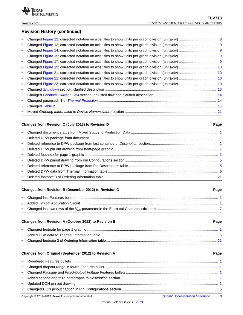
Output Current (mA)
Dro
pout
Vol
tage
(m
V)
0 15 30 45 60 75 90 105 120 135 1500
50
100
150
200
250
300
350VOUT = 1.8VVOUT = 3.3V
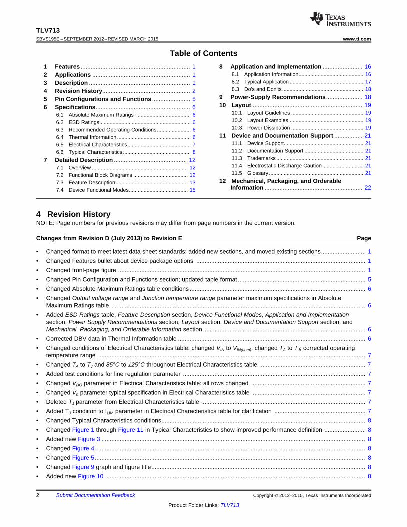
TLV713
IN
EN
OUT
GND
COUTCIN
OptionalOptionalON
OFF
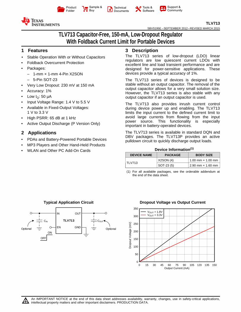
Product
Folder
Sample &Buy
Technical
Documents
Tools &
Software
Support &Community
TLV713SBVS195E –SEPTEMBER 2012–REVISED MARCH 2015
TLV713 Capacitor-Free, 150-mA, Low-Dropout RegulatorWith Foldback Current Limit for Portable Devices
1 Features 3 DescriptionThe TLV713 series of low-dropout (LDO) linear
1• Stable Operation With or Without Capacitorsregulators are low quiescent current LDOs with• Foldback Overcurrent Protection excellent line and load transient performance and are
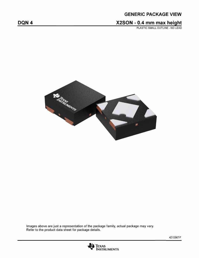
• Packages: designed for power-sensitive applications. Thesedevices provide a typical accuracy of 1%.– 1-mm × 1-mm 4-Pin X2SON
– 5-Pin SOT-23 The TLV713 series of devices is designed to bestable without an output capacitor. The removal of the• Very Low Dropout: 230 mV at 150 mAoutput capacitor allows for a very small solution size.• Accuracy: 1% However, the TLV713 series is also stable with any
• Low IQ: 50 µA output capacitor if an output capacitor is used.• Input Voltage Range: 1.4 V to 5.5 V The TLV713 also provides inrush current control• Available in Fixed-Output Voltages: during device power up and enabling. The TLV713
1 V to 3.3 V limits the input current to the defined current limit toavoid large currents from flowing from the input• High PSRR: 65 dB at 1 kHzpower source. This functionality is especially• Active Output Discharge (P Version Only) important in battery-operated devices.
The TLV713 series is available in standard DQN and2 ApplicationsDBV packages. The TLV713P provides an active
• PDAs and Battery-Powered Portable Devices pulldown circuit to quickly discharge output loads.• MP3 Players and Other Hand-Held Products
Device Information(1)• WLAN and Other PC Add-On CardsDEVICE NAME PACKAGE BODY SIZE
X2SON (4) 1.00 mm × 1.00 mmTLV713
SOT-23 (5) 2.90 mm × 1.60 mm
(1) For all available packages, see the orderable addendum atthe end of the data sheet.
space
space
space
Typical Application Circuit Dropout Voltage vs Output Current
1
An IMPORTANT NOTICE at the end of this data sheet addresses availability, warranty, changes, use in safety-critical applications,intellectual property matters and other important disclaimers. PRODUCTION DATA.
TLV713SBVS195E –SEPTEMBER 2012–REVISED MARCH 2015 www.ti.com
Table of Contents1 Features .................................................................. 1 8 Application and Implementation ........................ 16
8.1 Application Information............................................ 162 Applications ........................................................... 18.2 Typical Application .................................................. 173 Description ............................................................. 18.3 Do's and Don'ts....................................................... 184 Revision History..................................................... 2
9 Power-Supply Recommendations...................... 185 Pin Configurations and Functions ....................... 510 Layout................................................................... 196 Specifications......................................................... 6
10.1 Layout Guidelines ................................................. 196.1 Absolute Maximum Ratings ..................................... 610.2 Layout Examples................................................... 196.2 ESD Ratings.............................................................. 610.3 Power Dissipation ................................................. 196.3 Recommended Operating Conditions....................... 6
11 Device and Documentation Support ................. 216.4 Thermal Information .................................................. 611.1 Device Support...................................................... 216.5 Electrical Characteristics........................................... 711.2 Documentation Support ........................................ 216.6 Typical Characteristics .............................................. 811.3 Trademarks ........................................................... 217 Detailed Description ............................................ 1211.4 Electrostatic Discharge Caution............................ 217.1 Overview ................................................................. 1211.5 Glossary ................................................................ 217.2 Functional Block Diagrams ..................................... 12
12 Mechanical, Packaging, and Orderable7.3 Feature Description................................................. 13Information ........................................................... 227.4 Device Functional Modes........................................ 15
4 Revision HistoryNOTE: Page numbers for previous revisions may differ from page numbers in the current version.
Changes from Revision D (July 2013) to Revision E Page
• Changed format to meet latest data sheet standards; added new sections, and moved existing sections........................... 1• Changed Features bullet about device package options ...................................................................................................... 1• Changed front-page figure ..................................................................................................................................................... 1• Changed Pin Configuration and Functions section; updated table format ............................................................................. 5• Changed Absolute Maximum Ratings table conditions .......................................................................................................... 6• Changed Output voltage range and Junction temperature range parameter maximum specifications in Absolute
Maximum Ratings table ......................................................................................................................................................... 6• Added ESD Ratings table, Feature Description section, Device Functional Modes, Application and Implementation
section, Power Supply Recommendations section, Layout section, Device and Documentation Support section, andMechanical, Packaging, and Orderable Information section .................................................................................................. 6
• Corrected DBV data in Thermal Information table ................................................................................................................. 6• Changed conditions of Electrical Characteristics table: changed VIN to VIN(nom); changed TA to TJ; corrected operating
temperature range ................................................................................................................................................................. 7• Changed TA to TJ and 85°C to 125°C throughout Electrical Characteristics table ................................................................ 7• Added test conditions for line regulation parameter .............................................................................................................. 7• Changed VDO parameter in Electrical Characteristics table: all rows changed ..................................................................... 7• Changed Vn parameter typical specification in Electrical Characteristics table .................................................................... 7• Deleted TJ parameter from Electrical Characteristics table ................................................................................................... 7• Added TJ condiiton to ILIM parameter in Electrical Characteristics table for clarification ....................................................... 7• Changed Typical Characteristics conditions........................................................................................................................... 8• Changed Figure 1 through Figure 11 in Typical Characteristics to show improved performance definition ......................... 8• Added new Figure 3 ............................................................................................................................................................... 8• Changed Figure 4................................................................................................................................................................... 8• Changed Figure 5................................................................................................................................................................... 8• Changed Figure 9 graph and figure title................................................................................................................................. 8• Added new Figure 10 ............................................................................................................................................................ 8
2 Submit Documentation Feedback Copyright © 2012–2015, Texas Instruments Incorporated
Product Folder Links: TLV713
TLV713www.ti.com SBVS195E –SEPTEMBER 2012–REVISED MARCH 2015
Revision History (continued)• Changed Figure 12; corrected notation on axis titles to show units per graph division (units/div) ........................................ 8• Changed Figure 13; corrected notation on axis titles to show units per graph division (units/div) ........................................ 9• Changed Figure 14; corrected notation on axis titles to show units per graph division (units/div) ........................................ 9• Changed Figure 15; corrected notation on axis titles to show units per graph division (units/div) ........................................ 9• Changed Figure 17; corrected notation on axis titles to show units per graph division (units/div) ........................................ 9• Changed Figure 19; corrected notation on axis titles to show units per graph division (units/div) ...................................... 10• Changed Figure 21; corrected notation on axis titles to show units per graph division (units/div) ...................................... 10• Changed Figure 22; corrected notation on axis titles to show units per graph division (units/div) ...................................... 10• Changed Figure 23; corrected notation on axis titles to show units per graph division (units/div) ...................................... 10• Changed Shutdown section: clarified description ................................................................................................................ 13• Changed Foldback Current Limit section: adjusted flow and clarified description ............................................................... 14• Changed paragraph 1 of Thermal Protection ...................................................................................................................... 14• Changed Table 2 ................................................................................................................................................................. 17• Moved Ordering Information to Device Nomenclature section ............................................................................................ 21
Changes from Revision C (July 2013) to Revision D Page
• Changed document status from Mixed Status to Production Data ........................................................................................ 1• Deleted DPW package from document .................................................................................................................................. 1• Deleted reference to DPW package from last sentence of Description section..................................................................... 1• Deleted DPW pin out drawing from front-page graphic.......................................................................................................... 1• Deleted footnote for page 1 graphic ....................................................................................................................................... 1• Deleted DPW pinout drawing from Pin Configurations section .............................................................................................. 5• Deleted reference to DPW package from Pin Descriptions table........................................................................................... 5• Deleted DPW data from Thermal Information table ............................................................................................................... 6• Deleted footnote 3 of Ordering Information table ................................................................................................................. 21
Changes from Revision B (December 2012) to Revision C Page
• Changed last Features bullet.................................................................................................................................................. 1• Added Typical Application Circuit ........................................................................................................................................... 1• Changed last two rows of the VDO parameter in the Electrical Characteristics table ............................................................. 7
Changes from Revision A (October 2012) to Revision B Page
• Changed footnote for page 1 graphic..................................................................................................................................... 1• Added DBV data to Thermal Information table....................................................................................................................... 6• Changed footnote 3 of Ordering Information table ............................................................................................................... 21
Changes from Original (September 2012) to Revision A Page
• Reordered Features bullets .................................................................................................................................................... 1• Changed dropout range in fourth Features bullet................................................................................................................... 1• Changed Package and Fixed-Output Voltage Features bullets ............................................................................................. 1• Added second and third paragraphs to Description section................................................................................................... 1• Updated DQN pin out drawing................................................................................................................................................ 1• Changed DQN pinout caption in Pin Configurations section.................................................................................................. 5
Copyright © 2012–2015, Texas Instruments Incorporated Submit Documentation Feedback 3
Product Folder Links: TLV713
TLV713SBVS195E –SEPTEMBER 2012–REVISED MARCH 2015 www.ti.com
• Changed 1.2 V to 0.9 V in description of EN pin in Pin Descriptions table............................................................................ 5• Changed DQN header row in Thermal Information table....................................................................................................... 6• Changed VOUT maximum specification in Electrical Characteristics table.............................................................................. 7• Combined all VDO rows together in Electrical Characteristics table ....................................................................................... 7• Changed VDO specifications in Electrical Characteristics table .............................................................................................. 7• Changed ISHDN test conditions in Electrical Characteristics table ........................................................................................... 7• Changed Typical Characteristics conditions........................................................................................................................... 8• Added curves.......................................................................................................................................................................... 8• Changed junction temperature range in second paragraph of Overview section ................................................................ 12• Updated Figure 24................................................................................................................................................................ 12• Deleted third paragraph from Thermal Information section.................................................................................................. 14• Changed second paragraph of Input and Output Capacitor Considerations section ........................................................... 16• Deleted curve reference from Dropout Voltage section ....................................................................................................... 16
4 Submit Documentation Feedback Copyright © 2012–2015, Texas Instruments Incorporated
Product Folder Links: TLV713
OUT GND
IN EN
1 2
4 31
2
3
5
4
OUT
NC
IN
GND
EN
TLV713www.ti.com SBVS195E –SEPTEMBER 2012–REVISED MARCH 2015
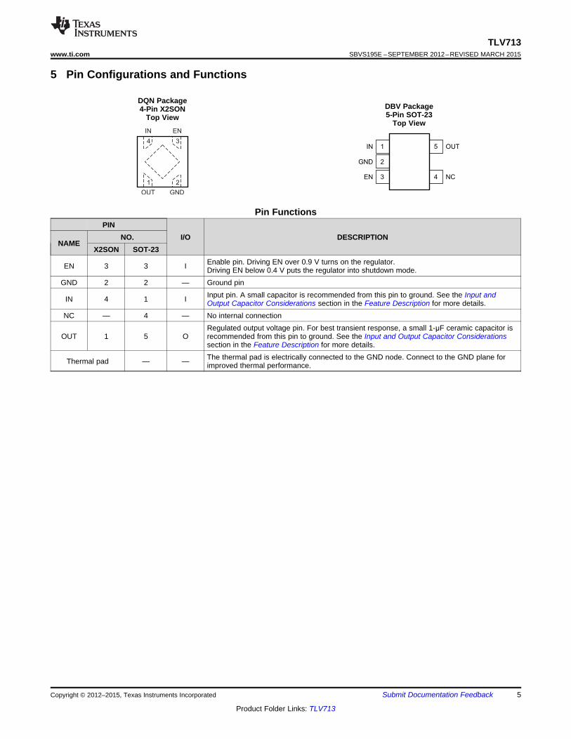
5 Pin Configurations and Functions
DQN PackageDBV Package4-Pin X2SON5-Pin SOT-23Top View
Top View
Pin FunctionsPIN
NO. I/O DESCRIPTIONNAME
X2SON SOT-23Enable pin. Driving EN over 0.9 V turns on the regulator.EN 3 3 I Driving EN below 0.4 V puts the regulator into shutdown mode.
GND 2 2 — Ground pinInput pin. A small capacitor is recommended from this pin to ground. See the Input andIN 4 1 I Output Capacitor Considerations section in the Feature Description for more details.
NC — 4 — No internal connectionRegulated output voltage pin. For best transient response, a small 1-μF ceramic capacitor is
OUT 1 5 O recommended from this pin to ground. See the Input and Output Capacitor Considerationssection in the Feature Description for more details.The thermal pad is electrically connected to the GND node. Connect to the GND plane forThermal pad — — improved thermal performance.
Copyright © 2012–2015, Texas Instruments Incorporated Submit Documentation Feedback 5
Product Folder Links: TLV713
TLV713SBVS195E –SEPTEMBER 2012–REVISED MARCH 2015 www.ti.com
6 Specifications
6.1 Absolute Maximum RatingsOver operating junction temperature range (TJ = 25°C), unless otherwise noted. All voltages are with respect to GND. (1)
MIN MAX UNITInput, VIN –0.3 6
Voltage Enable, VEN –0.3 VIN + 0.3 VOutput, VOUT –0.3 3.6
Current Maximum output, IOUT(max) Internally limitedOutput short-circuit duration IndefiniteTotal power dissipation Continuous, PD(tot) See Thermal Information
Storage, Tstg –55 150 °CTemperature
Junction, TJ –55 125 °C
(1) Stresses beyond those listed under Absolute Maximum Ratings may cause permanent damage to the device. These are stress ratingsonly, which do not imply functional operation of the device at these or any other conditions beyond those indicated under RecommendedOperating Conditions. Exposure to absolute-maximum-rated conditions for extended periods may affect device reliability.
6.2 ESD RatingsVALUE UNIT
Human body model (HBM), per ANSI/ESDA/JEDEC JS-001, all pins (1) ±2000V(ESD) Electrostatic discharge VCharged device model (CDM), per JEDEC specification JESD22-C101, ±500all pins (2)
(1) JEDEC document JEP155 states that 500-V HBM allows safe manufacturing with a standard ESD control process.(2) JEDEC document JEP157 states that 250-V CDM allows safe manufacturing with a standard ESD control process.
6.3 Recommended Operating Conditionsover operating junction temperature range (unless otherwise noted).
MIN NOM MAX UNITVIN Input voltage 1.4 5.5 VVEN Enable range 0 VIN VIOUT Output current 0 150 mACIN Input capacitor 0 1 µFCOUT Output capacitor 0 0.1 100 µFTJ Operating junction temperature range –40 125 °C
6.4 Thermal InformationTLV713, TLV713P
THERMAL METRIC (1) DQN (X2SON) DBV (SOT23) UNIT4 PINS 5 PINS
RθJA Junction-to-ambient thermal resistance 255.8 249RθJC(top) Junction-to-case (top) thermal resistance 159.3 172.7RθJB Junction-to-board thermal resistance 208.2 76.7
°C/WψJT Junction-to-top characterization parameter 16.2 49.7ψJB Junction-to-board characterization parameter 208.1 75.8RθJC(bot) Junction-to-case (bottom) thermal resistance 148.6 n/a
(1) For more information about traditional and new thermal metrics, see the IC Package Thermal Metrics application report, SPRA953.
6 Submit Documentation Feedback Copyright © 2012–2015, Texas Instruments Incorporated
Product Folder Links: TLV713
TLV713www.ti.com SBVS195E –SEPTEMBER 2012–REVISED MARCH 2015
6.5 Electrical CharacteristicsOver operating temperature range (TJ = –40°C to 125°C), VIN(nom) = VOUT(nom) + 0.5 V or VIN(nom) = 2 V (whichever is greater),IOUT = 1 mA, VEN = VIN, and COUT = 0.47 µF, unless otherwise noted. Typical values are at TJ = 25°C.
PARAMETER TEST CONDITIONS MIN TYP MAX UNIT
VIN Input voltage range 1.4 5.5 V
Output voltageVOUT 1 3.3 Vrange
VOUT ≥ 1.8 V, TJ = 25°C –1% 1%
VOUT < 1.8 V, TJ = 25°C –20 20 mVDC output accuracy
VOUT ≥ 1.2 V, –40°C ≤ TJ ≤ 125°C –1.5% 1.5%
VOUT < 1.2 V, –40°C ≤ TJ ≤ 125°C –50 50 mV
ΔVOUT(ΔVIN) Line regulation Max {VOUT(nom) + 0.5 V, VIN = 2.0 V} ≤ VIN ≤ 5.5 V 1 5 mV
ΔVOUT(ΔIOUT) Load regulation 0 mA ≤ IOUT ≤ 150 mA 10 30 mV
1 V ≤ VOUT < 1.8 V, IOUT = 150 mA 600 900
VOUT = 1.1 V, IOUT = 100 mA 470 600
1.8 V ≤ VOUT < 2.1 V, IOUT = 30 mA 70
1.8 V ≤ VOUT < 2.1 V, IOUT = 150 mA 350 575
2.1 V ≤ VOUT < 2.5 V, IOUT = 30 mA 90VOUT = 0.98 × VOUT(nom),TJ = –40°C to 85°C 2.1 V ≤ VOUT < 2.5 V, IOUT = 150 mA 290 481
2.5 V ≤ VOUT < 3 V, IOUT = 30 mA 50
2.5 V ≤ VOUT < 3 V, IOUT = 150 mA 246 445VDO Dropout voltage mV
3 V ≤ VOUT < 3.6 V, IOUT = 30 mA 46
3 V ≤ VOUT < 3.6 V, IOUT = 150 mA 230 420
1 V ≤ VOUT < 1.8 V, IOUT = 150 mA 600 1020
VOUT = 1.1 V, IOUT = 100 mA 470 720
1.8 V ≤ VOUT < 2.1 V, IOUT = 150 mA 350 695VOUT = 0.98 × VOUT(nom),TJ = –40°C to 125°C 2.1 V ≤ VOUT < 2.5 V, IOUT = 150 mA 290 601
2.5 V ≤ VOUT < 3 V, IOUT = 150 mA 246 565
3 V ≤ VOUT < 3.6 V, IOUT = 150 mA 230 540
IGND Ground pin current IOUT = 0 mA 50 75 µA
ISHUTDOWN Shutdown current VEN ≤ 0.4 V, 2.0 V ≤ VIN ≤ 5.5 V, TJ = 25°C 0.1 1 µA
f = 100 Hz 70VIN = 3.3 V,Power-supplyPSRR VOUT = 2.8 V, f = 10 kHz 55 dBrejection ratio IOUT = 30 mA f = 1 MHz 55
Vn Output noise voltage BW = 100 Hz to 100 kHz, VIN = 2.3 V, VOUT = 1.8 V, IOUT = 10 mA 73 µVRMS
tSTR Start-up time (1) COUT = 1.0 μF, IOUT = 150 mA 100 µs
Enable highVHI 0.9 VIN V(enabled)
Enable lowVLO 0 0.4 V(disabled)
IEN EN pin current EN = 5.5 V 0.01 µA
Pulldown resistorRPULLDOWN VIN = 4 V 120 Ω(TLV713P only)
VIN = 3.8 V, VOUT = 3.3 V, TJ = –40 to 85°C 180
ILIM Output current limit VIN = 2.25 V, VOUT = 1.8 V, TJ = –40 to 85°C 180 mA
VIN = 2.0 V, VOUT = 1.2 V, TJ = –40 to 85°C 180
ISC Short-circuit current VOUT = 0 V 40 mA
Shutdown, temperature increasing 158TSD Thermal shutdown °C
Reset, temperature decreasing 140
(1) Start-up time is the time from EN assertion to (0.98 × VOUT(nom)).
Copyright © 2012–2015, Texas Instruments Incorporated Submit Documentation Feedback 7
Product Folder Links: TLV713
Output Current (mA)
Dro
pout
Vol
tage
(m
V)
0 25 50 75 100 125 1500
50
100
150
200
250
300
350
400TJ = -40qCTJ = 0qCTJ = 25qCTJ = 85qCTJ = 125qC
Input Voltage (V)
Gro
und
Pin
Cur
rent
(P
A)
2 2.5 3 3.5 4 4.5 5 5.530
32.535
37.540
42.545
47.550
52.555
57.560
62.565
TJ = -40qCTJ = 0qCTJ = 25qCTJ = 85qCTJ = 125qC
Temperature (qC)
Out
put V
olta
ge (
V)
-40 -20 0 20 40 60 80 100 120 1401.794
1.7945
1.795
1.7955
1.796
1.7965
1.797
1.7975
1.798
Output Current (mA)
Dro
pout
Vol
tage
(m
V)
0 25 50 75 100 125 1500
100
200
300
400
500TJ = -40qCTJ = 0qCTJ = 25qCTJ = 85qCTJ = 125qC
Input Voltage (V)
Out
put V
olta
ge (
V)
2 2.5 3 3.5 4 4.5 5 5.51.793
1.794
1.795
1.796
1.797
1.798
1.799
1.8
1.801
1.802TJ = -40qCTJ = 0qCTJ = 25qCTJ = 85qCTJ = 125qC
Output Current (mA)
Out
put V
olta
ge (
V)
0 20 40 60 80 100 120 140 1601.786
1.788
1.79
1.792
1.794
1.796
1.798
1.8TJ = -40qCTJ = 0qCTJ = 25qCTJ = 85qCTJ = 125qC
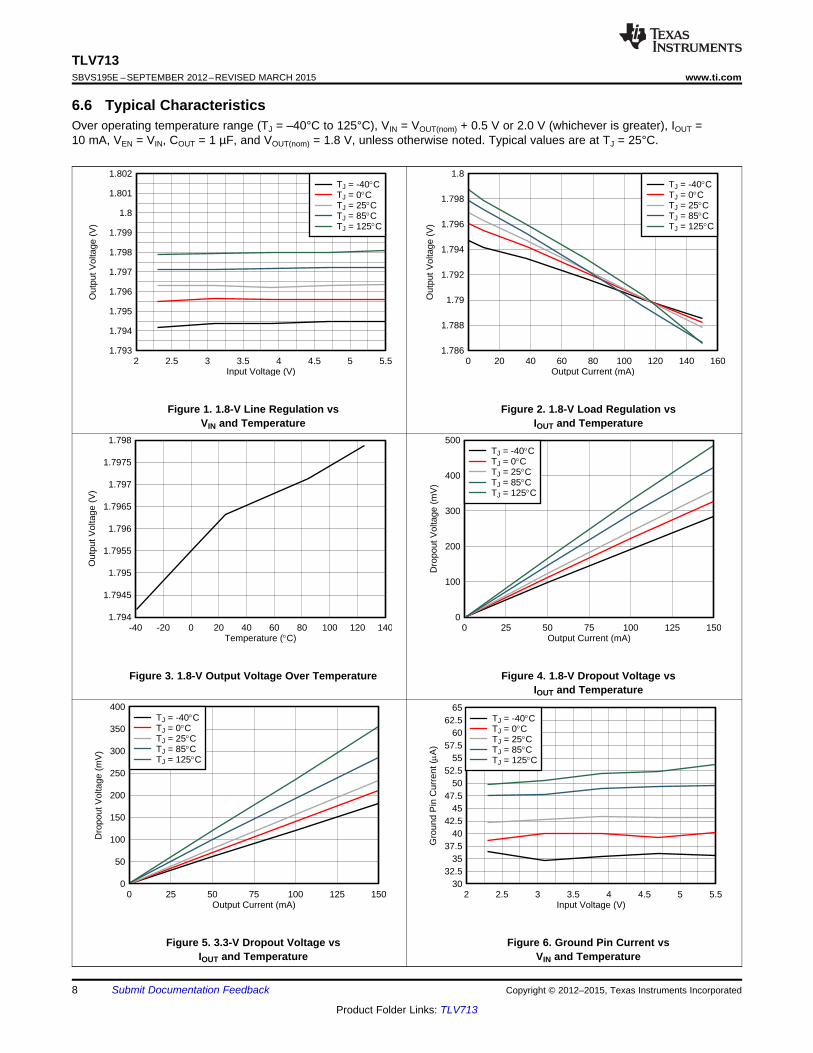
TLV713SBVS195E –SEPTEMBER 2012–REVISED MARCH 2015 www.ti.com
6.6 Typical CharacteristicsOver operating temperature range (TJ = –40°C to 125°C), VIN = VOUT(nom) + 0.5 V or 2.0 V (whichever is greater), IOUT =10 mA, VEN = VIN, COUT = 1 µF, and VOUT(nom) = 1.8 V, unless otherwise noted. Typical values are at TJ = 25°C.
Figure 1. 1.8-V Line Regulation vs Figure 2. 1.8-V Load Regulation vsVIN and Temperature IOUT and Temperature
Figure 3. 1.8-V Output Voltage Over Temperature Figure 4. 1.8-V Dropout Voltage vsIOUT and Temperature
Figure 5. 3.3-V Dropout Voltage vs Figure 6. Ground Pin Current vsIOUT and Temperature VIN and Temperature
8 Submit Documentation Feedback Copyright © 2012–2015, Texas Instruments Incorporated
Product Folder Links: TLV713
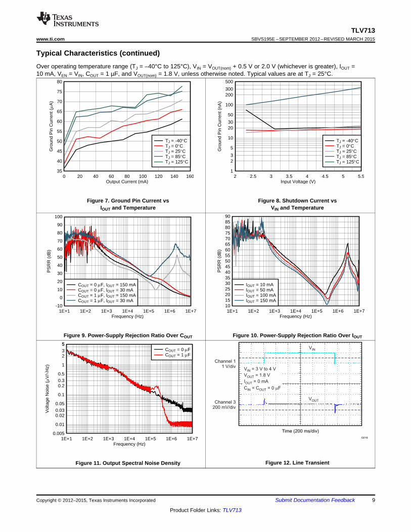
Frequency (Hz)
Vol
tage
Noi
se (P
V/�
Hz)
1E+1 1E+2 1E+3 1E+4 1E+5 1E+6 1E+70.005
0.01
0.020.030.05
0.1
0.20.30.5
1
2355
COUT = 0 PFCOUT = 1 PF
Time (200 ms/div)
Channel 11 V/div
Channel 3200 mV/div
V = 3 V to 4 V
C =
IN
OUT
IN OUT
V = 1.8 V
I = 0 mA
C = 0 F
OUT
m
VIN
G016
VOUT
Frequency (Hz)
PS
RR
(dB
)
1E+1 1E+2 1E+3 1E+4 1E+5 1E+6 1E+7-10
0
10
20
30
40
50
60
70
80
90
100
COUT = 0 PF, IOUT = 150 mACOUT = 0 PF, IOUT = 30 mACOUT = 1 PF, IOUT = 150 mACOUT = 1 PF, IOUT = 30 mA
Frequency (Hz)
PS
RR
(dB
)
1E+1 1E+2 1E+3 1E+4 1E+5 1E+6 1E+71015202530354045505560657075808590
IOUT = 10 mAIOUT = 50 mAIOUT = 100 mAIOUT = 150 mA
Output Current (mA)
Gro
und
Pin
Cur
rent
(P
A)
0 20 40 60 80 100 120 140 16035
40
45
50
55
60
65
70
75
80
TJ = -40qCTJ = 0qCTJ = 25qCTJ = 85qCTJ = 125qC
Input Voltage (V)
Gro
und
Pin
Cur
rent
(nA
)
2 2.5 3 3.5 4 4.5 5 5.51
23
5
10
2030
50
100
200300
500
TJ = -40qCTJ = 0qCTJ = 25qCTJ = 85qCTJ = 125qC
TLV713www.ti.com SBVS195E –SEPTEMBER 2012–REVISED MARCH 2015
Typical Characteristics (continued)Over operating temperature range (TJ = –40°C to 125°C), VIN = VOUT(nom) + 0.5 V or 2.0 V (whichever is greater), IOUT =10 mA, VEN = VIN, COUT = 1 µF, and VOUT(nom) = 1.8 V, unless otherwise noted. Typical values are at TJ = 25°C.
Figure 7. Ground Pin Current vs Figure 8. Shutdown Current vsIOUT and Temperature VIN and Temperature
Figure 9. Power-Supply Rejection Ratio Over COUT Figure 10. Power-Supply Rejection Ratio Over IOUT
Figure 12. Line TransientFigure 11. Output Spectral Noise Density
Copyright © 2012–2015, Texas Instruments Incorporated Submit Documentation Feedback 9
Product Folder Links: TLV713
0
0.25
0.5
0.75
1
1.25
1.5
1.75
2
0 50 100 150 200 250 300 350Output Current (mA)
Out
put V
olta
ge (
V)
TLV71318P
G011
Time (200 ms/div)
Channel 30.5 V/div
Channel 450 mA/div
V = 5 V, V = 1.8 V
C = C =IN OUT
IN OUT 0 Fm
VOUT
G013
IOUT
0
0.5
1
1.5
2
2.5
3
3.5
0 50 100 150 200 250 300Output Current (mA)
Out
put V
olta
ge (
V)
TLV71333P
G010
Time (200 ms/div)
Channel 3200 mV/div
Channel 420 mA/div
V = 5 V, V = 1.8 V
C = C =IN OUT
IN OUT 0 Fm
VOUT
G015
IOUT
Time (200 ms/div)
Channel 11 V/div
Channel 30.5 V/div
V = 3 V to 4 V
V = 1.8 V
I = 150 mA
C = C =
IN
OUT
IN OUT
OUT
0 Fm
VIN
G017
VOUT
Time (200 ms/div)
Channel 120 mV/div
Channel 420 mA/div
V = 5 V, V = 1.8 V
C = C =IN OUT
IN OUT 1 Fm
VOUT
G012
IOUT
TLV713SBVS195E –SEPTEMBER 2012–REVISED MARCH 2015 www.ti.com
Typical Characteristics (continued)Over operating temperature range (TJ = –40°C to 125°C), VIN = VOUT(nom) + 0.5 V or 2.0 V (whichever is greater), IOUT =10 mA, VEN = VIN, COUT = 1 µF, and VOUT(nom) = 1.8 V, unless otherwise noted. Typical values are at TJ = 25°C.
Figure 13. Line Transient Figure 14. 0-mA to 20-mA Load Transient
Figure 15. 0-mA to 20-mA Load Transient Figure 16. 3.3-V Output Voltage vs Output Current(Foldback Current Limit)
Figure 17. 0-mA to 100-mA Load Transient Figure 18. 1.8-V Output Voltage vs Output Current(Foldback Current Limit)
10 Submit Documentation Feedback Copyright © 2012–2015, Texas Instruments Incorporated
Product Folder Links: TLV713
Time (50 ms/div)
Channel 12 V/div
Channel 31 V/div
V = 3 V
V = 1.8 V
C = C =
IN
IN OUT
OUT
1 F
TPS71318PNo Load
m
VIN
G019
VOUT
Channel 22 V/div
Channel 4100 mA/div
EN
IOUT
Time (50 ms/div)
Channel 12 V/div
Channel 31 V/div
V = 3 V
V = 1.8 V
C = C =
IN
IN OUT
OUT
OUT
0 F
I = 150 mA
TLV71318P
m
VIN
G021
VOUT
Channel 22 V/div
Channel 450 mA/div
EN
IOUT
Time (100 s/div)m
Channel 1100 mV/div
Channel 31 V/div
V = 2.3 V, V = 1.8 V
C = 1 F, C = 1OUTIN
IN OUT
OUT
m m0 F
I = 90 mA
TLV71318P, From Design
VIN
G022
VOUT
Channel 21 V/div
Channel 450 mA/div
EN
ILOAD
0
1
2
3
4
0 0.5 1 1.5 2Time (s)
Vol
tage
(V
)
VIN VOUT
IOUT = 150 mATPS71318P
G020
Time (200 ms/div)
Channel 3200 mV/div
Channel 450 mA/div
V = 5 V, V = 1.8 V
C = C =IN OUT
IN OUT 0 Fm
VOUT
G014
IOUT
TLV713www.ti.com SBVS195E –SEPTEMBER 2012–REVISED MARCH 2015
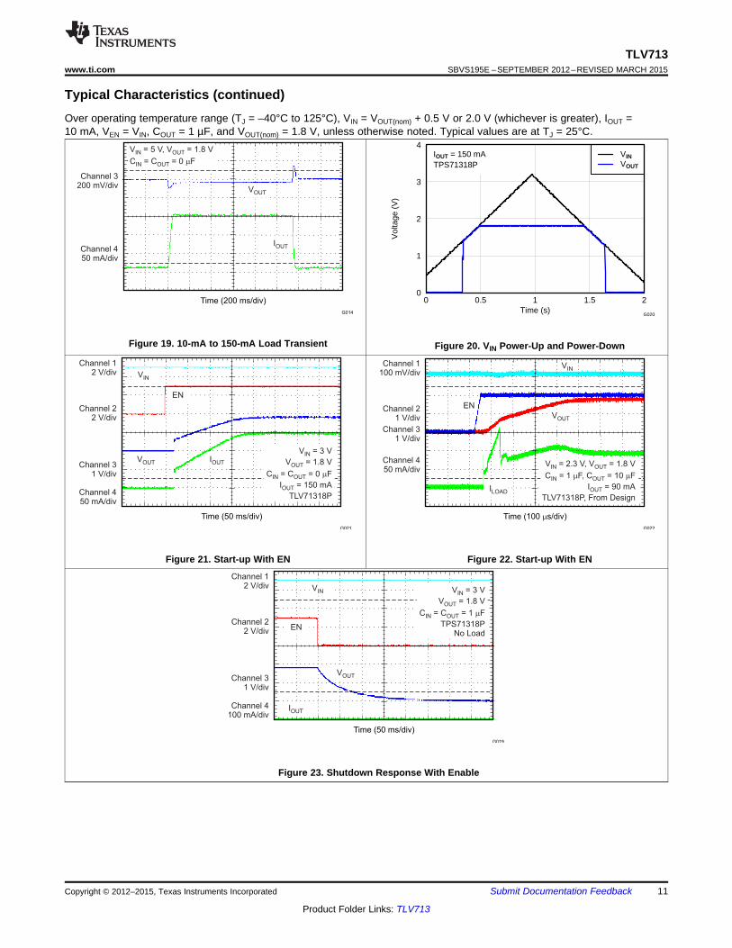
Typical Characteristics (continued)Over operating temperature range (TJ = –40°C to 125°C), VIN = VOUT(nom) + 0.5 V or 2.0 V (whichever is greater), IOUT =10 mA, VEN = VIN, COUT = 1 µF, and VOUT(nom) = 1.8 V, unless otherwise noted. Typical values are at TJ = 25°C.
Figure 19. 10-mA to 150-mA Load Transient Figure 20. VIN Power-Up and Power-Down
Figure 21. Start-up With EN Figure 22. Start-up With EN
Figure 23. Shutdown Response With Enable
Copyright © 2012–2015, Texas Instruments Incorporated Submit Documentation Feedback 11
Product Folder Links: TLV713
CurrentLimit
Bandgap
IN
EN
OUT
Logic
GND
TLV713
ThermalShutdown
UVLO
TLV713SBVS195E –SEPTEMBER 2012–REVISED MARCH 2015 www.ti.com
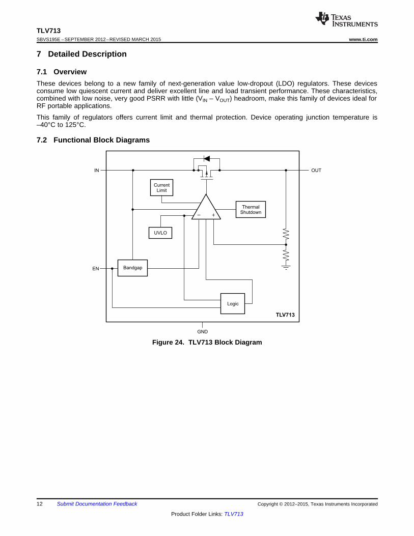
7 Detailed Description
7.1 OverviewThese devices belong to a new family of next-generation value low-dropout (LDO) regulators. These devicesconsume low quiescent current and deliver excellent line and load transient performance. These characteristics,combined with low noise, very good PSRR with little (VIN – VOUT) headroom, make this family of devices ideal forRF portable applications.
This family of regulators offers current limit and thermal protection. Device operating junction temperature is–40°C to 125°C.
7.2 Functional Block Diagrams
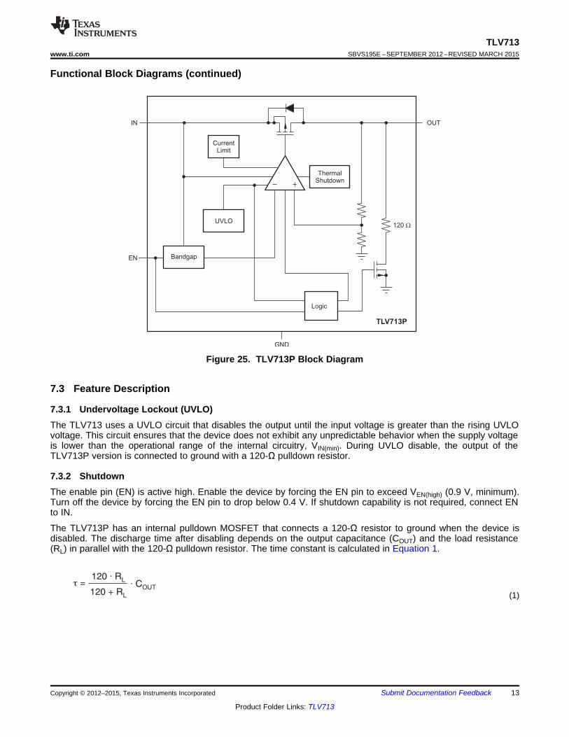
Figure 24. TLV713 Block Diagram
12 Submit Documentation Feedback Copyright © 2012–2015, Texas Instruments Incorporated
Product Folder Links: TLV713
t =120 · R
L
120 + RL
· COUT
CurrentLimit
UVLO
Bandgap
IN
EN
OUT
Logic
GND
TLV713P
120 W
ThermalShutdown
TLV713www.ti.com SBVS195E –SEPTEMBER 2012–REVISED MARCH 2015
Functional Block Diagrams (continued)
Figure 25. TLV713P Block Diagram
7.3 Feature Description
7.3.1 Undervoltage Lockout (UVLO)The TLV713 uses a UVLO circuit that disables the output until the input voltage is greater than the rising UVLOvoltage. This circuit ensures that the device does not exhibit any unpredictable behavior when the supply voltageis lower than the operational range of the internal circuitry, VIN(min). During UVLO disable, the output of theTLV713P version is connected to ground with a 120-Ω pulldown resistor.
7.3.2 ShutdownThe enable pin (EN) is active high. Enable the device by forcing the EN pin to exceed VEN(high) (0.9 V, minimum).Turn off the device by forcing the EN pin to drop below 0.4 V. If shutdown capability is not required, connect ENto IN.
The TLV713P has an internal pulldown MOSFET that connects a 120-Ω resistor to ground when the device isdisabled. The discharge time after disabling depends on the output capacitance (COUT) and the load resistance(RL) in parallel with the 120-Ω pulldown resistor. The time constant is calculated in Equation 1.
(1)
Copyright © 2012–2015, Texas Instruments Incorporated Submit Documentation Feedback 13
Product Folder Links: TLV713
TLV713SBVS195E –SEPTEMBER 2012–REVISED MARCH 2015 www.ti.com
Feature Description (continued)7.3.3 Foldback Current LimitThe TLV713 has an internal foldback current limit that helps protect the regulator during fault conditions. Thecurrent supplied by the device is gradually reducedwhile the output voltage decreases. When the output isshorted, the LDO supplies a typical current of 40 mA. Output voltage is not regulated when the device is incurrent limit, and is calculated by Equation 2:
VOUT = ILIMIT × RLOAD (2)
The PMOS pass transistor dissipates [(VIN – VOUT) × ILIMIT] until thermal shutdown is triggered and the deviceturns off. The device is turned on by the internal thermal shutdown circuit during cool down. If the fault conditioncontinues, the device cycles between current limit and thermal shutdown. See the Thermal Information sectionfor more details.
The TLV713 PMOS pass element has a built-in body diode that conducts current when the voltage at OUTexceeds the voltage at IN. This current is not limited, so if extended reverse voltage operation is anticipated,external limiting to 5% of the rated output current is recommended.
7.3.4 Thermal ProtectionThermal protection disables the output when the junction temperature rises to approximately 158°C, allowing thedevice to cool. When the junction temperature cools to approximately 140°C, the output circuitry is againenabled. Depending on power dissipation, thermal resistance, and ambient temperature, the thermal protectioncircuit may cycle on and off. This cycling limits regulator dissipation, protecting the device from damage as aresult of overheating.
Any tendency to activate the thermal protection circuit indicates excessive power dissipation or an inadequateheatsink. For reliable operation, junction temperature must be limited to 125°C maximum. To estimate the marginof safety in a complete design (including heatsink), increase the ambient temperature until the thermal protectionis triggered; use worst-case loads and signal conditions.
The TLV713 internal protection circuitry is designed to protect against overload conditions. This circuitry is notintended to replace proper heatsinking. Continuously running the TLV713 into thermal shutdown degrades devicereliability.
14 Submit Documentation Feedback Copyright © 2012–2015, Texas Instruments Incorporated
Product Folder Links: TLV713
TLV713www.ti.com SBVS195E –SEPTEMBER 2012–REVISED MARCH 2015
7.4 Device Functional Modes
7.4.1 Normal OperationThe device regulates to the nominal output voltage under the following conditions:• The input voltage is at least as high as VIN(min).• The input voltage is greater than the nominal output voltage added to the dropout voltage.• The enable voltage has previously exceeded the enable rising threshold voltage and has not decreased
below the enable falling threshold.• The output current is less than the current limit.• The device junction temperature is less than the maximum specified junction temperature.
7.4.2 Dropout OperationIf the input voltage is lower than the nominal output voltage plus the specified dropout voltage, but all otherconditions are met for normal operation, the device operates in dropout mode. In this mode of operation, theoutput voltage is the same as the input voltage minus the dropout voltage. The transient performance of thedevice is significantly degraded because the pass device is in the linear region and no longer controls the currentthrough the LDO. Line or load transients in dropout can result in large output voltage deviations.
7.4.3 DisabledThe device is disabled under the following conditions:• The enable voltage is less than the enable falling threshold voltage or has not yet exceeded the enable rising
threshold.• The device junction temperature is greater than the thermal shutdown temperature.
Table 1 shows the conditions that lead to the different modes of operation.
Table 1. Device Functional Mode ComparisonPARAMETER
OPERATING MODEVIN VEN IOUT TJ
VIN > VOUT(nom) + VDO andNormal mode VEN > VEN(high) IOUT < ILIM TJ < 125°CVIN > VIN(min)
Dropout mode VIN(min) < VIN < VOUT(nom) + VDO VEN > VEN(high) — TJ < 125°CDisabled mode(any true condition disables the — VEN < VEN(low) — TJ > 158°Cdevice)
Copyright © 2012–2015, Texas Instruments Incorporated Submit Documentation Feedback 15
Product Folder Links: TLV713
TLV713SBVS195E –SEPTEMBER 2012–REVISED MARCH 2015 www.ti.com
8 Application and Implementation
NOTEInformation in the following applications sections is not part of the TI componentspecification, and TI does not warrant its accuracy or completeness. TI’s customers areresponsible for determining suitability of components for their purposes. Customers shouldvalidate and test their design implementation to confirm system functionality.
8.1 Application Information
8.1.1 Input and Output Capacitor ConsiderationsThe TLV713 uses an advanced internal control loop to obtain stable operation both with and without the use ofinput or output capacitors. The TLV713 dynamic performance is improved with the use of an output capacitor. Anoutput capacitance of 0.1 μF or larger generally provides good dynamic response. X5R- and X7R-type ceramiccapacitors are recommended because these capacitors have minimal variation in value and equivalent seriesresistance (ESR) over temperature.
Although an input capacitor is not required for stability, it is good analog design practice to connect a 0.1-µF to1-µF capacitor from IN to GND. This capacitor counteracts reactive input sources and improves transientresponse, input ripple, and PSRR. An input capacitor is recommended if the source impedance is more than0.5 Ω. A higher-value capacitor may be necessary if large, fast, rise-time load transients are anticipated or if thedevice is located several inches from the input power source.
8.1.2 Dropout VoltageThe TLV713 uses a PMOS pass transistor to achieve low dropout. When (VIN – VOUT) is less than the dropoutvoltage (VDO), the PMOS pass device is in the linear region of operation and the input-to-output resistance is theRDS(on) of the PMOS pass element. VDO scales approximately with output current because the PMOS devicebehaves like a resistor in dropout. As with any linear regulator, PSRR and transient response are degraded as(VIN – VOUT) approaches dropout.
8.1.3 Transient ResponseAs with any regulator, increasing the size of the output capacitor reduces over- and undershoot magnitude butincreases the duration of the transient response.
16 Submit Documentation Feedback Copyright © 2012–2015, Texas Instruments Incorporated
Product Folder Links: TLV713
OUT
GND
VI
0.1 Fm
IN
EN0.1 Fm
V
(1.8 V to 3.6 V)O
MSP430
TLV713www.ti.com SBVS195E –SEPTEMBER 2012–REVISED MARCH 2015
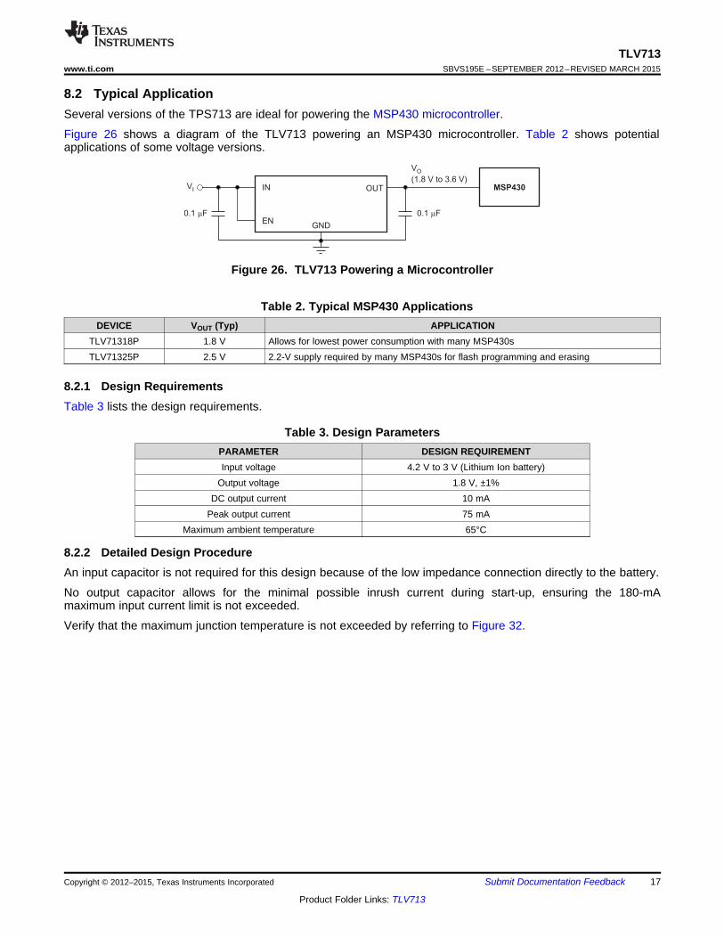
8.2 Typical ApplicationSeveral versions of the TPS713 are ideal for powering the MSP430 microcontroller.
Figure 26 shows a diagram of the TLV713 powering an MSP430 microcontroller. Table 2 shows potentialapplications of some voltage versions.
Figure 26. TLV713 Powering a Microcontroller
Table 2. Typical MSP430 ApplicationsDEVICE VOUT (Typ) APPLICATION
TLV71318P 1.8 V Allows for lowest power consumption with many MSP430sTLV71325P 2.5 V 2.2-V supply required by many MSP430s for flash programming and erasing
8.2.1 Design RequirementsTable 3 lists the design requirements.
Table 3. Design ParametersPARAMETER DESIGN REQUIREMENTInput voltage 4.2 V to 3 V (Lithium Ion battery)
Output voltage 1.8 V, ±1%DC output current 10 mA
Peak output current 75 mAMaximum ambient temperature 65°C
8.2.2 Detailed Design ProcedureAn input capacitor is not required for this design because of the low impedance connection directly to the battery.
No output capacitor allows for the minimal possible inrush current during start-up, ensuring the 180-mAmaximum input current limit is not exceeded.
Verify that the maximum junction temperature is not exceeded by referring to Figure 32.
Copyright © 2012–2015, Texas Instruments Incorporated Submit Documentation Feedback 17
Product Folder Links: TLV713
0
1
2
3
4
0 0.5 1 1.5 2Time (s)
Vol
tage
(V
)
VIN VOUT
IOUT = 150 mATPS71318P
G020
Frequency (Hz)
PS
RR
(dB
)
1E+1 1E+2 1E+3 1E+4 1E+5 1E+6 1E+7-10
0
10
20
30
40
50
60
70
80
90
100
COUT = 0 PF, IOUT = 150 mACOUT = 0 PF, IOUT = 30 mACOUT = 1 PF, IOUT = 150 mACOUT = 1 PF, IOUT = 30 mA 0
1
2
3
4
10 100 1k 10k 100kFrequency (Hz)
Vol
tage
( µV
/ H
z )
VOUT = 1.8 VIOUT = 10 mA
G009
TLV713SBVS195E –SEPTEMBER 2012–REVISED MARCH 2015 www.ti.com
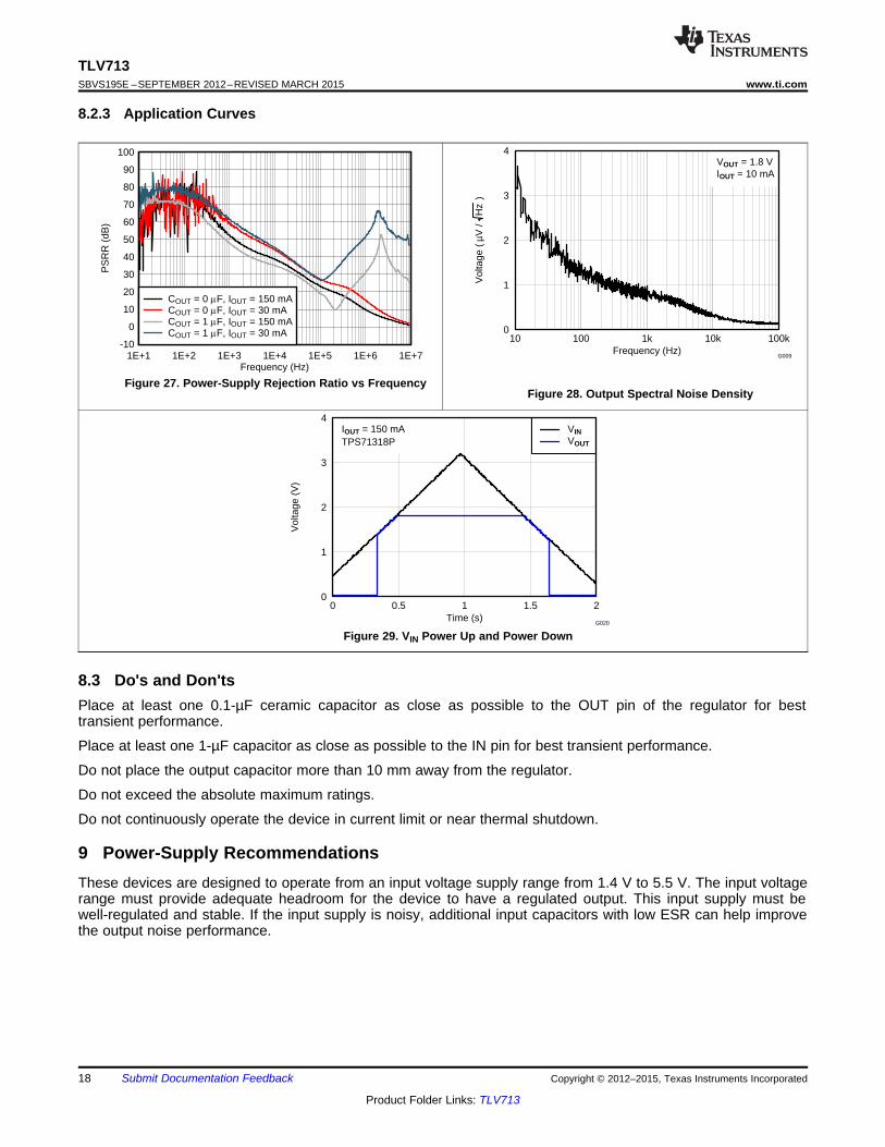
8.2.3 Application Curves
Figure 27. Power-Supply Rejection Ratio vs FrequencyFigure 28. Output Spectral Noise Density
Figure 29. VIN Power Up and Power Down
8.3 Do's and Don'tsPlace at least one 0.1-µF ceramic capacitor as close as possible to the OUT pin of the regulator for besttransient performance.
Place at least one 1-µF capacitor as close as possible to the IN pin for best transient performance.
Do not place the output capacitor more than 10 mm away from the regulator.
Do not exceed the absolute maximum ratings.
Do not continuously operate the device in current limit or near thermal shutdown.
9 Power-Supply RecommendationsThese devices are designed to operate from an input voltage supply range from 1.4 V to 5.5 V. The input voltagerange must provide adequate headroom for the device to have a regulated output. This input supply must bewell-regulated and stable. If the input supply is noisy, additional input capacitors with low ESR can help improvethe output noise performance.
18 Submit Documentation Feedback Copyright © 2012–2015, Texas Instruments Incorporated
Product Folder Links: TLV713
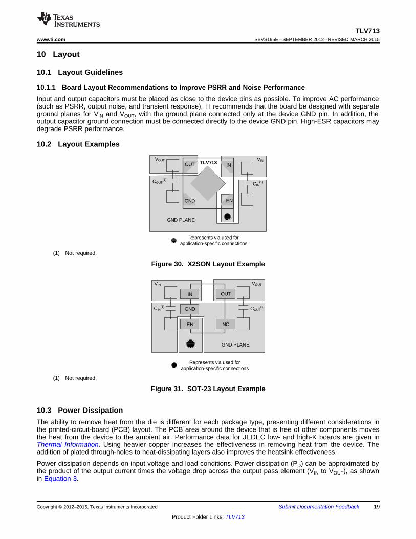
COUT(1)
VOUTVIN
GND PLANE
CIN(1)
Represents via used for application-specific connections
IN
GND
EN NC
OUT
COUT(1)
VOUT VIN
GND PLANE
CIN(1)
TLV713
Represents via used for application-specific connections
OUT
GND EN
IN
TLV713www.ti.com SBVS195E –SEPTEMBER 2012–REVISED MARCH 2015
10 Layout
10.1 Layout Guidelines
10.1.1 Board Layout Recommendations to Improve PSRR and Noise PerformanceInput and output capacitors must be placed as close to the device pins as possible. To improve AC performance(such as PSRR, output noise, and transient response), TI recommends that the board be designed with separateground planes for VIN and VOUT, with the ground plane connected only at the device GND pin. In addition, theoutput capacitor ground connection must be connected directly to the device GND pin. High-ESR capacitors maydegrade PSRR performance.
10.2 Layout Examples
(1) Not required.
Figure 30. X2SON Layout Example
(1) Not required.
Figure 31. SOT-23 Layout Example
10.3 Power DissipationThe ability to remove heat from the die is different for each package type, presenting different considerations inthe printed-circuit-board (PCB) layout. The PCB area around the device that is free of other components movesthe heat from the device to the ambient air. Performance data for JEDEC low- and high-K boards are given inThermal Information. Using heavier copper increases the effectiveness in removing heat from the device. Theaddition of plated through-holes to heat-dissipating layers also improves the heatsink effectiveness.
Power dissipation depends on input voltage and load conditions. Power dissipation (PD) can be approximated bythe product of the output current times the voltage drop across the output pass element (VIN to VOUT), as shownin Equation 3.
Copyright © 2012–2015, Texas Instruments Incorporated Submit Documentation Feedback 19
Product Folder Links: TLV713
Y YJT J T JT D
: T = T + P·
Y YJB J B JB D
: T = T + P·
Power Dissipation (W)
Max
imum
Am
bien
t Tem
pera
ture
(°C
)
0 0.05 0.1 0.15 0.2 0.25 0.3 0.3550
60
70
80
90
100
110
120
130TLV713 DQN, High-K LayoutTLV713 DBV, High-K Layout
TLV713SBVS195E –SEPTEMBER 2012–REVISED MARCH 2015 www.ti.com
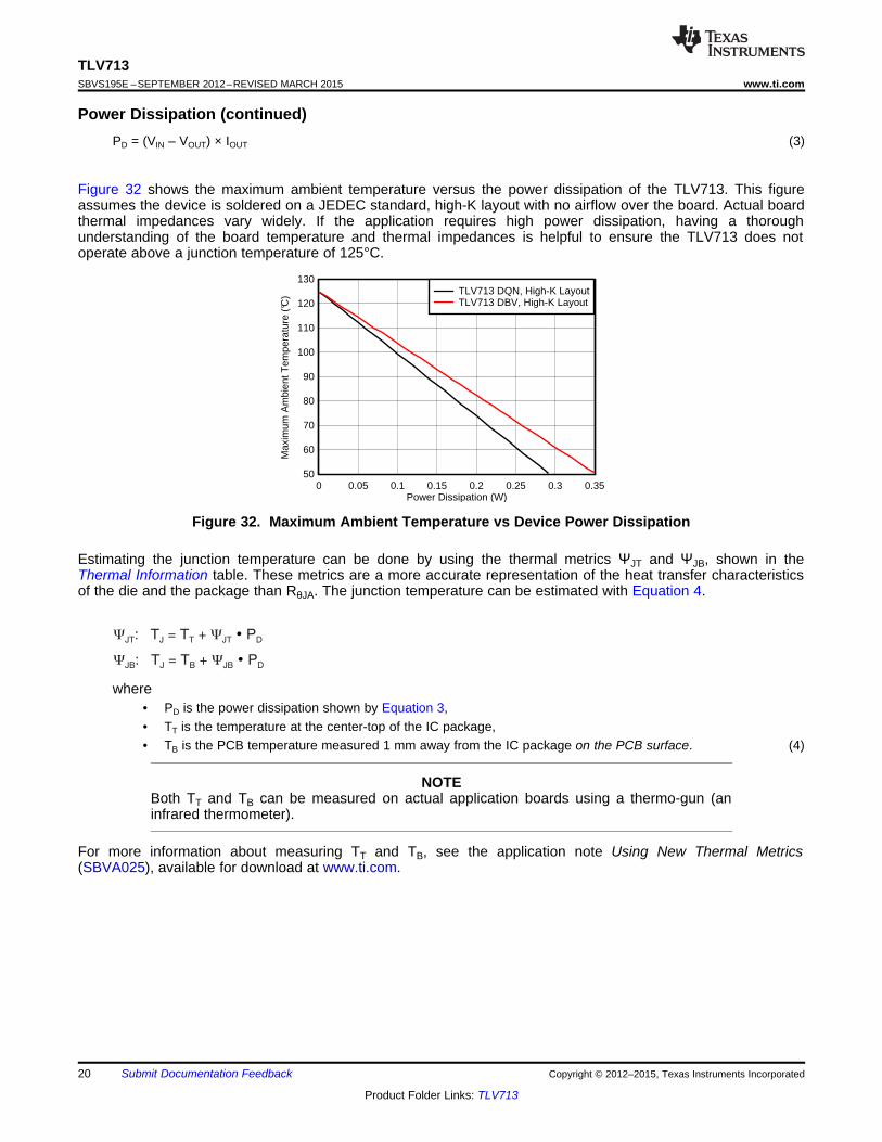
Power Dissipation (continued)PD = (VIN – VOUT) × IOUT (3)
Figure 32 shows the maximum ambient temperature versus the power dissipation of the TLV713. This figureassumes the device is soldered on a JEDEC standard, high-K layout with no airflow over the board. Actual boardthermal impedances vary widely. If the application requires high power dissipation, having a thoroughunderstanding of the board temperature and thermal impedances is helpful to ensure the TLV713 does notoperate above a junction temperature of 125°C.
Figure 32. Maximum Ambient Temperature vs Device Power Dissipation
Estimating the junction temperature can be done by using the thermal metrics ΨJT and ΨJB, shown in theThermal Information table. These metrics are a more accurate representation of the heat transfer characteristicsof the die and the package than RθJA. The junction temperature can be estimated with Equation 4.
where• PD is the power dissipation shown by Equation 3,• TT is the temperature at the center-top of the IC package,• TB is the PCB temperature measured 1 mm away from the IC package on the PCB surface. (4)
NOTEBoth TT and TB can be measured on actual application boards using a thermo-gun (aninfrared thermometer).
For more information about measuring TT and TB, see the application note Using New Thermal Metrics(SBVA025), available for download at www.ti.com.
20 Submit Documentation Feedback Copyright © 2012–2015, Texas Instruments Incorporated
Product Folder Links: TLV713
TLV713www.ti.com SBVS195E –SEPTEMBER 2012–REVISED MARCH 2015
11 Device and Documentation Support
11.1 Device Support
11.1.1 Development Support
11.1.1.1 Evaluation ModulesThree evaluation modules (EVMs) are available to assist in the initial circuit performance evaluation using theTLV713:• TLV71312PEVM-171• TLV71318PEVM-171• TLV71333PEVM-171
These EVMs can be requested at the Texas Instruments website through the device product folders orpurchased directly from the TI eStore.
11.1.1.2 Spice ModelsComputer simulation of circuit performance using SPICE is often useful when analyzing the performance ofanalog circuits and systems. A SPICE model for the TLV713 is available through the product folders under Tools& Software.
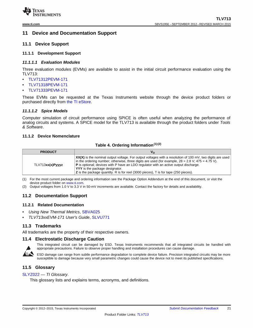
11.1.2 Device Nomenclature
Table 4. Ordering Information (1) (2)
PRODUCT VO
XX(X) is the nominal output voltage. For output voltages with a resolution of 100 mV, two digits are usedin the ordering number; otherwise, three digits are used (for example, 28 = 2.8 V; 475 = 4.75 V).
TLV713xx(x)Pyyyz P is optional; devices with P have an LDO regulator with an active output discharge.YYY is the package designator.Z is the package quantity. R is for reel (3000 pieces), T is for tape (250 pieces).
(1) For the most current package and ordering information see the Package Option Addendum at the end of this document, or visit thedevice product folder on www.ti.com.
(2) Output voltages from 1.0 V to 3.3 V in 50-mV increments are available. Contact the factory for details and availability.
11.2 Documentation Support
11.2.1 Related Documentation• Using New Thermal Metrics, SBVA025• TLV713xxEVM-171 User's Guide, SLVU771
11.3 TrademarksAll trademarks are the property of their respective owners.
11.4 Electrostatic Discharge CautionThis integrated circuit can be damaged by ESD. Texas Instruments recommends that all integrated circuits be handled withappropriate precautions. Failure to observe proper handling and installation procedures can cause damage.
ESD damage can range from subtle performance degradation to complete device failure. Precision integrated circuits may be moresusceptible to damage because very small parametric changes could cause the device not to meet its published specifications.
11.5 GlossarySLYZ022 — TI Glossary.
This glossary lists and explains terms, acronyms, and definitions.
Copyright © 2012–2015, Texas Instruments Incorporated Submit Documentation Feedback 21
Product Folder Links: TLV713
TLV713SBVS195E –SEPTEMBER 2012–REVISED MARCH 2015 www.ti.com
12 Mechanical, Packaging, and Orderable InformationThe following pages include mechanical, packaging, and orderable information. This information is the mostcurrent data available for the designated devices. This data is subject to change without notice and revision ofthis document. For browser-based versions of this data sheet, refer to the left-hand navigation.
22 Submit Documentation Feedback Copyright © 2012–2015, Texas Instruments Incorporated
Product Folder Links: TLV713
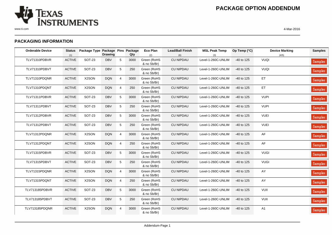
PACKAGE OPTION ADDENDUM
www.ti.com 4-Mar-2016
Addendum-Page 1
PACKAGING INFORMATION
Orderable Device Status(1)
Package Type PackageDrawing
Pins PackageQty
Eco Plan(2)
Lead/Ball Finish(6)
MSL Peak Temp(3)
Op Temp (°C) Device Marking(4/5)
Samples
TLV71310PDBVR ACTIVE SOT-23 DBV 5 3000 Green (RoHS& no Sb/Br)
CU NIPDAU Level-1-260C-UNLIM -40 to 125 VUQI
TLV71310PDBVT ACTIVE SOT-23 DBV 5 250 Green (RoHS& no Sb/Br)
CU NIPDAU Level-1-260C-UNLIM -40 to 125 VUQI
TLV71310PDQNR ACTIVE X2SON DQN 4 3000 Green (RoHS& no Sb/Br)
CU NIPDAU Level-1-260C-UNLIM -40 to 125 ET
TLV71310PDQNT ACTIVE X2SON DQN 4 250 Green (RoHS& no Sb/Br)
CU NIPDAU Level-1-260C-UNLIM -40 to 125 ET
TLV71311PDBVR ACTIVE SOT-23 DBV 5 3000 Green (RoHS& no Sb/Br)
CU NIPDAU Level-1-260C-UNLIM -40 to 125 VUPI
TLV71311PDBVT ACTIVE SOT-23 DBV 5 250 Green (RoHS& no Sb/Br)
CU NIPDAU Level-1-260C-UNLIM -40 to 125 VUPI
TLV71312PDBVR ACTIVE SOT-23 DBV 5 3000 Green (RoHS& no Sb/Br)
CU NIPDAU Level-1-260C-UNLIM -40 to 125 VUEI
TLV71312PDBVT ACTIVE SOT-23 DBV 5 250 Green (RoHS& no Sb/Br)
CU NIPDAU Level-1-260C-UNLIM -40 to 125 VUEI
TLV71312PDQNR ACTIVE X2SON DQN 4 3000 Green (RoHS& no Sb/Br)
CU NIPDAU Level-1-260C-UNLIM -40 to 125 AF
TLV71312PDQNT ACTIVE X2SON DQN 4 250 Green (RoHS& no Sb/Br)
CU NIPDAU Level-1-260C-UNLIM -40 to 125 AF
TLV71315PDBVR ACTIVE SOT-23 DBV 5 3000 Green (RoHS& no Sb/Br)
CU NIPDAU Level-1-260C-UNLIM -40 to 125 VUGI
TLV71315PDBVT ACTIVE SOT-23 DBV 5 250 Green (RoHS& no Sb/Br)
CU NIPDAU Level-1-260C-UNLIM -40 to 125 VUGI
TLV71315PDQNR ACTIVE X2SON DQN 4 3000 Green (RoHS& no Sb/Br)
CU NIPDAU Level-1-260C-UNLIM -40 to 125 AY
TLV71315PDQNT ACTIVE X2SON DQN 4 250 Green (RoHS& no Sb/Br)
CU NIPDAU Level-1-260C-UNLIM -40 to 125 AY
TLV713185PDBVR ACTIVE SOT-23 DBV 5 3000 Green (RoHS& no Sb/Br)
CU NIPDAU Level-1-260C-UNLIM -40 to 125 VUII
TLV713185PDBVT ACTIVE SOT-23 DBV 5 250 Green (RoHS& no Sb/Br)
CU NIPDAU Level-1-260C-UNLIM -40 to 125 VUII
TLV713185PDQNR ACTIVE X2SON DQN 4 3000 Green (RoHS& no Sb/Br)
CU NIPDAU Level-1-260C-UNLIM -40 to 125 A1
PACKAGE OPTION ADDENDUM
www.ti.com 4-Mar-2016
Addendum-Page 2
Orderable Device Status(1)
Package Type PackageDrawing
Pins PackageQty
Eco Plan(2)
Lead/Ball Finish(6)
MSL Peak Temp(3)
Op Temp (°C) Device Marking(4/5)
Samples
TLV713185PDQNT ACTIVE X2SON DQN 4 250 Green (RoHS& no Sb/Br)
CU NIPDAU Level-1-260C-UNLIM -40 to 125 A1
TLV71318PDBVR ACTIVE SOT-23 DBV 5 3000 Green (RoHS& no Sb/Br)
CU NIPDAU Level-1-260C-UNLIM -40 to 125 VUDI
TLV71318PDBVT ACTIVE SOT-23 DBV 5 250 Green (RoHS& no Sb/Br)
CU NIPDAU Level-1-260C-UNLIM -40 to 125 VUDI
TLV71318PDQNR ACTIVE X2SON DQN 4 3000 Green (RoHS& no Sb/Br)
CU NIPDAU Level-1-260C-UNLIM -40 to 125 AW
TLV71318PDQNT ACTIVE X2SON DQN 4 250 Green (RoHS& no Sb/Br)
CU NIPDAU Level-1-260C-UNLIM -40 to 125 AW
TLV71320DQNR ACTIVE X2SON DQN 4 3000 Green (RoHS& no Sb/Br)
CU NIPDAU Level-1-260C-UNLIM -40 to 85 B2
TLV71320DQNT ACTIVE X2SON DQN 4 250 Green (RoHS& no Sb/Br)
CU NIPDAU Level-1-260C-UNLIM -40 to 85 B2
TLV71325PDBVR ACTIVE SOT-23 DBV 5 3000 Green (RoHS& no Sb/Br)
CU NIPDAU Level-1-260C-UNLIM -40 to 125 VUJI
TLV71325PDBVT ACTIVE SOT-23 DBV 5 250 Green (RoHS& no Sb/Br)
CU NIPDAU Level-1-260C-UNLIM -40 to 125 VUJI
TLV71325PDQNR ACTIVE X2SON DQN 4 3000 Green (RoHS& no Sb/Br)
CU NIPDAU Level-1-260C-UNLIM -40 to 125 AZ
TLV71325PDQNT ACTIVE X2SON DQN 4 250 Green (RoHS& no Sb/Br)
CU NIPDAU Level-1-260C-UNLIM -40 to 125 AZ
TLV713285PDBVR ACTIVE SOT-23 DBV 5 3000 Green (RoHS& no Sb/Br)
CU NIPDAU Level-1-260C-UNLIM -40 to 125 VULI
TLV713285PDBVT ACTIVE SOT-23 DBV 5 250 Green (RoHS& no Sb/Br)
CU NIPDAU Level-1-260C-UNLIM -40 to 125 VULI
TLV713285PDQNR ACTIVE X2SON DQN 4 3000 Green (RoHS& no Sb/Br)
CU NIPDAU Level-1-260C-UNLIM -40 to 125 A2
TLV713285PDQNT ACTIVE X2SON DQN 4 250 Green (RoHS& no Sb/Br)
CU NIPDAU Level-1-260C-UNLIM -40 to 125 A2
TLV71328PDBVR ACTIVE SOT-23 DBV 5 3000 Green (RoHS& no Sb/Br)
CU NIPDAU Level-1-260C-UNLIM -40 to 125 VUKI
TLV71328PDBVT ACTIVE SOT-23 DBV 5 250 Green (RoHS& no Sb/Br)
CU NIPDAU Level-1-260C-UNLIM -40 to 125 VUKI
TLV71328PDQNR ACTIVE X2SON DQN 4 3000 Green (RoHS& no Sb/Br)
CU NIPDAU Level-1-260C-UNLIM -40 to 125 AK
PACKAGE OPTION ADDENDUM
www.ti.com 4-Mar-2016
Addendum-Page 3
Orderable Device Status(1)
Package Type PackageDrawing
Pins PackageQty
Eco Plan(2)
Lead/Ball Finish(6)
MSL Peak Temp(3)
Op Temp (°C) Device Marking(4/5)
Samples
TLV71328PDQNT ACTIVE X2SON DQN 4 250 Green (RoHS& no Sb/Br)
CU NIPDAU Level-1-260C-UNLIM -40 to 125 AK
TLV71330PDBVR ACTIVE SOT-23 DBV 5 3000 Green (RoHS& no Sb/Br)
CU NIPDAU Level-1-260C-UNLIM -40 to 125 VUMI
TLV71330PDBVT ACTIVE SOT-23 DBV 5 250 Green (RoHS& no Sb/Br)
CU NIPDAU Level-1-260C-UNLIM -40 to 125 VUMI
TLV71330PDQNR ACTIVE X2SON DQN 4 3000 Green (RoHS& no Sb/Br)
CU NIPDAU Level-1-260C-UNLIM -40 to 125 AL
TLV71330PDQNT ACTIVE X2SON DQN 4 250 Green (RoHS& no Sb/Br)
CU NIPDAU Level-1-260C-UNLIM -40 to 125 AL
TLV71333PDBVR ACTIVE SOT-23 DBV 5 3000 Green (RoHS& no Sb/Br)
CU NIPDAU Level-1-260C-UNLIM -40 to 125 VUFI
TLV71333PDBVT ACTIVE SOT-23 DBV 5 250 Green (RoHS& no Sb/Br)
CU NIPDAU Level-1-260C-UNLIM -40 to 125 VUFI
TLV71333PDQNR ACTIVE X2SON DQN 4 3000 Green (RoHS& no Sb/Br)
CU NIPDAU Level-1-260C-UNLIM -40 to 125 AH
TLV71333PDQNT ACTIVE X2SON DQN 4 250 Green (RoHS& no Sb/Br)
CU NIPDAU Level-1-260C-UNLIM -40 to 125 AH
(1) The marketing status values are defined as follows:ACTIVE: Product device recommended for new designs.LIFEBUY: TI has announced that the device will be discontinued, and a lifetime-buy period is in effect.NRND: Not recommended for new designs. Device is in production to support existing customers, but TI does not recommend using this part in a new design.PREVIEW: Device has been announced but is not in production. Samples may or may not be available.OBSOLETE: TI has discontinued the production of the device.
(2) Eco Plan - The planned eco-friendly classification: Pb-Free (RoHS), Pb-Free (RoHS Exempt), or Green (RoHS & no Sb/Br) - please check http://www.ti.com/productcontent for the latest availabilityinformation and additional product content details.TBD: The Pb-Free/Green conversion plan has not been defined.Pb-Free (RoHS): TI's terms "Lead-Free" or "Pb-Free" mean semiconductor products that are compatible with the current RoHS requirements for all 6 substances, including the requirement thatlead not exceed 0.1% by weight in homogeneous materials. Where designed to be soldered at high temperatures, TI Pb-Free products are suitable for use in specified lead-free processes.Pb-Free (RoHS Exempt): This component has a RoHS exemption for either 1) lead-based flip-chip solder bumps used between the die and package, or 2) lead-based die adhesive used betweenthe die and leadframe. The component is otherwise considered Pb-Free (RoHS compatible) as defined above.Green (RoHS & no Sb/Br): TI defines "Green" to mean Pb-Free (RoHS compatible), and free of Bromine (Br) and Antimony (Sb) based flame retardants (Br or Sb do not exceed 0.1% by weightin homogeneous material)
(3) MSL, Peak Temp. - The Moisture Sensitivity Level rating according to the JEDEC industry standard classifications, and peak solder temperature.
PACKAGE OPTION ADDENDUM
www.ti.com 4-Mar-2016
Addendum-Page 4
(4) There may be additional marking, which relates to the logo, the lot trace code information, or the environmental category on the device.
(5) Multiple Device Markings will be inside parentheses. Only one Device Marking contained in parentheses and separated by a "~" will appear on a device. If a line is indented then it is a continuationof the previous line and the two combined represent the entire Device Marking for that device.
(6) Lead/Ball Finish - Orderable Devices may have multiple material finish options. Finish options are separated by a vertical ruled line. Lead/Ball Finish values may wrap to two lines if the finishvalue exceeds the maximum column width.
Important Information and Disclaimer:The information provided on this page represents TI's knowledge and belief as of the date that it is provided. TI bases its knowledge and belief on informationprovided by third parties, and makes no representation or warranty as to the accuracy of such information. Efforts are underway to better integrate information from third parties. TI has taken andcontinues to take reasonable steps to provide representative and accurate information but may not have conducted destructive testing or chemical analysis on incoming materials and chemicals.TI and TI suppliers consider certain information to be proprietary, and thus CAS numbers and other limited information may not be available for release.
In no event shall TI's liability arising out of such information exceed the total purchase price of the TI part(s) at issue in this document sold by TI to Customer on an annual basis.
OTHER QUALIFIED VERSIONS OF TLV713P :
• Automotive: TLV713P-Q1
NOTE: Qualified Version Definitions:
• Automotive - Q100 devices qualified for high-reliability automotive applications targeting zero defects
TAPE AND REEL INFORMATION
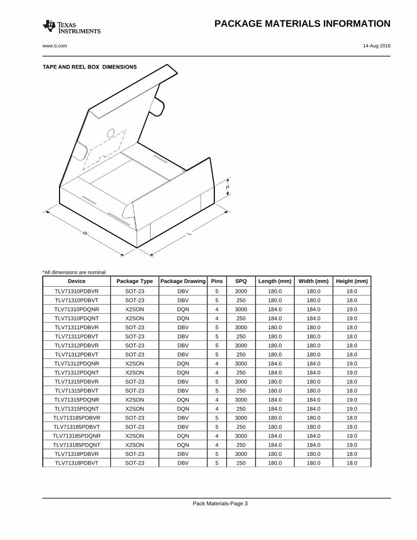
*All dimensions are nominal
Device PackageType
PackageDrawing
Pins SPQ ReelDiameter
(mm)
ReelWidth
W1 (mm)
A0(mm)
B0(mm)
K0(mm)
P1(mm)
W(mm)
Pin1Quadrant
TLV71310PDBVR SOT-23 DBV 5 3000 178.0 9.0 3.23 3.17 1.37 4.0 8.0 Q3
TLV71310PDBVT SOT-23 DBV 5 250 178.0 8.4 3.23 3.17 1.37 4.0 8.0 Q3
TLV71310PDQNR X2SON DQN 4 3000 180.0 9.5 1.16 1.16 0.5 4.0 8.0 Q2
TLV71310PDQNT X2SON DQN 4 250 180.0 9.5 1.16 1.16 0.5 4.0 8.0 Q2
TLV71311PDBVR SOT-23 DBV 5 3000 178.0 9.0 3.23 3.17 1.37 4.0 8.0 Q3
TLV71311PDBVT SOT-23 DBV 5 250 178.0 8.4 3.3 3.2 1.4 4.0 8.0 Q3
TLV71312PDBVR SOT-23 DBV 5 3000 178.0 9.0 3.23 3.17 1.37 4.0 8.0 Q3
TLV71312PDBVT SOT-23 DBV 5 250 178.0 8.4 3.23 3.17 1.37 4.0 8.0 Q3
TLV71312PDQNR X2SON DQN 4 3000 180.0 9.5 1.16 1.16 0.5 4.0 8.0 Q2
TLV71312PDQNT X2SON DQN 4 250 180.0 9.5 1.16 1.16 0.5 4.0 8.0 Q2
TLV71315PDBVR SOT-23 DBV 5 3000 178.0 9.0 3.23 3.17 1.37 4.0 8.0 Q3
TLV71315PDBVT SOT-23 DBV 5 250 178.0 8.4 3.23 3.17 1.37 4.0 8.0 Q3
TLV71315PDQNR X2SON DQN 4 3000 180.0 9.5 1.16 1.16 0.5 4.0 8.0 Q2
TLV71315PDQNT X2SON DQN 4 250 180.0 9.5 1.16 1.16 0.5 4.0 8.0 Q2
TLV713185PDBVR SOT-23 DBV 5 3000 178.0 9.0 3.23 3.17 1.37 4.0 8.0 Q3
TLV713185PDBVT SOT-23 DBV 5 250 178.0 8.4 3.23 3.17 1.37 4.0 8.0 Q3
TLV713185PDQNR X2SON DQN 4 3000 180.0 9.5 1.16 1.16 0.5 4.0 8.0 Q2
TLV713185PDQNT X2SON DQN 4 250 180.0 9.5 1.16 1.16 0.5 4.0 8.0 Q2
PACKAGE MATERIALS INFORMATION
www.ti.com 14-Aug-2016
Pack Materials-Page 1
Device PackageType
PackageDrawing
Pins SPQ ReelDiameter
(mm)
ReelWidth
W1 (mm)
A0(mm)
B0(mm)
K0(mm)
P1(mm)
W(mm)
Pin1Quadrant
TLV71318PDBVR SOT-23 DBV 5 3000 178.0 9.0 3.23 3.17 1.37 4.0 8.0 Q3
TLV71318PDBVT SOT-23 DBV 5 250 178.0 8.4 3.23 3.17 1.37 4.0 8.0 Q3
TLV71318PDQNR X2SON DQN 4 3000 180.0 9.5 1.16 1.16 0.5 4.0 8.0 Q2
TLV71318PDQNT X2SON DQN 4 250 180.0 9.5 1.16 1.16 0.5 4.0 8.0 Q2
TLV71320DQNR X2SON DQN 4 3000 180.0 9.5 1.16 1.16 0.5 4.0 8.0 Q2
TLV71320DQNT X2SON DQN 4 250 180.0 9.5 1.16 1.16 0.5 4.0 8.0 Q2
TLV71325PDBVR SOT-23 DBV 5 3000 178.0 9.0 3.23 3.17 1.37 4.0 8.0 Q3
TLV71325PDBVT SOT-23 DBV 5 250 178.0 8.4 3.23 3.17 1.37 4.0 8.0 Q3
TLV71325PDQNR X2SON DQN 4 3000 180.0 9.5 1.16 1.16 0.5 4.0 8.0 Q2
TLV71325PDQNT X2SON DQN 4 250 180.0 9.5 1.16 1.16 0.5 4.0 8.0 Q2
TLV713285PDBVR SOT-23 DBV 5 3000 178.0 9.0 3.23 3.17 1.37 4.0 8.0 Q3
TLV713285PDBVT SOT-23 DBV 5 250 178.0 8.4 3.23 3.17 1.37 4.0 8.0 Q3
TLV713285PDQNR X2SON DQN 4 3000 180.0 9.5 1.16 1.16 0.5 4.0 8.0 Q2
TLV713285PDQNT X2SON DQN 4 250 180.0 9.5 1.16 1.16 0.5 4.0 8.0 Q2
TLV71328PDBVR SOT-23 DBV 5 3000 178.0 9.0 3.23 3.17 1.37 4.0 8.0 Q3
TLV71328PDBVT SOT-23 DBV 5 250 178.0 8.4 3.23 3.17 1.37 4.0 8.0 Q3
TLV71328PDQNR X2SON DQN 4 3000 180.0 9.5 1.16 1.16 0.5 4.0 8.0 Q2
TLV71328PDQNT X2SON DQN 4 250 180.0 9.5 1.16 1.16 0.5 4.0 8.0 Q2
TLV71330PDBVR SOT-23 DBV 5 3000 178.0 9.0 3.23 3.17 1.37 4.0 8.0 Q3
TLV71330PDBVT SOT-23 DBV 5 250 178.0 8.4 3.23 3.17 1.37 4.0 8.0 Q3
TLV71330PDQNR X2SON DQN 4 3000 180.0 9.5 1.16 1.16 0.5 4.0 8.0 Q2
TLV71330PDQNT X2SON DQN 4 250 180.0 9.5 1.16 1.16 0.5 4.0 8.0 Q2
TLV71333PDBVR SOT-23 DBV 5 3000 178.0 9.0 3.3 3.2 1.4 4.0 8.0 Q3
TLV71333PDBVT SOT-23 DBV 5 250 178.0 8.4 3.23 3.17 1.37 4.0 8.0 Q3
TLV71333PDQNR X2SON DQN 4 3000 180.0 9.5 1.16 1.16 0.5 4.0 8.0 Q2
TLV71333PDQNT X2SON DQN 4 250 180.0 9.5 1.16 1.16 0.5 4.0 8.0 Q2
PACKAGE MATERIALS INFORMATION
www.ti.com 14-Aug-2016
Pack Materials-Page 2
*All dimensions are nominal
Device Package Type Package Drawing Pins SPQ Length (mm) Width (mm) Height (mm)
TLV71310PDBVR SOT-23 DBV 5 3000 180.0 180.0 18.0
TLV71310PDBVT SOT-23 DBV 5 250 180.0 180.0 18.0
TLV71310PDQNR X2SON DQN 4 3000 184.0 184.0 19.0
TLV71310PDQNT X2SON DQN 4 250 184.0 184.0 19.0
TLV71311PDBVR SOT-23 DBV 5 3000 180.0 180.0 18.0
TLV71311PDBVT SOT-23 DBV 5 250 180.0 180.0 18.0
TLV71312PDBVR SOT-23 DBV 5 3000 180.0 180.0 18.0
TLV71312PDBVT SOT-23 DBV 5 250 180.0 180.0 18.0
TLV71312PDQNR X2SON DQN 4 3000 184.0 184.0 19.0
TLV71312PDQNT X2SON DQN 4 250 184.0 184.0 19.0
TLV71315PDBVR SOT-23 DBV 5 3000 180.0 180.0 18.0
TLV71315PDBVT SOT-23 DBV 5 250 180.0 180.0 18.0
TLV71315PDQNR X2SON DQN 4 3000 184.0 184.0 19.0
TLV71315PDQNT X2SON DQN 4 250 184.0 184.0 19.0
TLV713185PDBVR SOT-23 DBV 5 3000 180.0 180.0 18.0
TLV713185PDBVT SOT-23 DBV 5 250 180.0 180.0 18.0
TLV713185PDQNR X2SON DQN 4 3000 184.0 184.0 19.0
TLV713185PDQNT X2SON DQN 4 250 184.0 184.0 19.0
TLV71318PDBVR SOT-23 DBV 5 3000 180.0 180.0 18.0
TLV71318PDBVT SOT-23 DBV 5 250 180.0 180.0 18.0
PACKAGE MATERIALS INFORMATION
www.ti.com 14-Aug-2016
Pack Materials-Page 3
Device Package Type Package Drawing Pins SPQ Length (mm) Width (mm) Height (mm)
TLV71318PDQNR X2SON DQN 4 3000 184.0 184.0 19.0
TLV71318PDQNT X2SON DQN 4 250 184.0 184.0 19.0
TLV71320DQNR X2SON DQN 4 3000 184.0 184.0 19.0
TLV71320DQNT X2SON DQN 4 250 184.0 184.0 19.0
TLV71325PDBVR SOT-23 DBV 5 3000 180.0 180.0 18.0
TLV71325PDBVT SOT-23 DBV 5 250 180.0 180.0 18.0
TLV71325PDQNR X2SON DQN 4 3000 184.0 184.0 19.0
TLV71325PDQNT X2SON DQN 4 250 184.0 184.0 19.0
TLV713285PDBVR SOT-23 DBV 5 3000 180.0 180.0 18.0
TLV713285PDBVT SOT-23 DBV 5 250 180.0 180.0 18.0
TLV713285PDQNR X2SON DQN 4 3000 184.0 184.0 19.0
TLV713285PDQNT X2SON DQN 4 250 184.0 184.0 19.0
TLV71328PDBVR SOT-23 DBV 5 3000 180.0 180.0 18.0
TLV71328PDBVT SOT-23 DBV 5 250 180.0 180.0 18.0
TLV71328PDQNR X2SON DQN 4 3000 184.0 184.0 19.0
TLV71328PDQNT X2SON DQN 4 250 184.0 184.0 19.0
TLV71330PDBVR SOT-23 DBV 5 3000 180.0 180.0 18.0
TLV71330PDBVT SOT-23 DBV 5 250 180.0 180.0 18.0
TLV71330PDQNR X2SON DQN 4 3000 184.0 184.0 19.0
TLV71330PDQNT X2SON DQN 4 250 184.0 184.0 19.0
TLV71333PDBVR SOT-23 DBV 5 3000 180.0 180.0 18.0
TLV71333PDBVT SOT-23 DBV 5 250 180.0 180.0 18.0
TLV71333PDQNR X2SON DQN 4 3000 184.0 184.0 19.0
TLV71333PDQNT X2SON DQN 4 250 184.0 184.0 19.0
PACKAGE MATERIALS INFORMATION
www.ti.com 14-Aug-2016
Pack Materials-Page 4
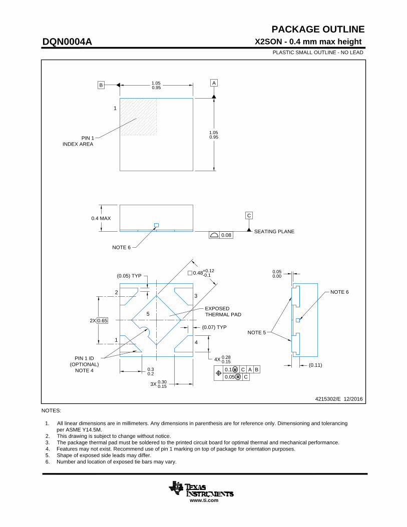
PACKAGE OUTLINE
DQN0004AX2SON - 0.4 mm max height
PLASTIC SMALL OUTLINE - NO LEAD
4215302/E 12/2016
NOTES:
1. All linear dimensions are in millimeters. Any dimensions in parenthesis are for reference only. Dimensioning and tolerancing
per ASME Y14.5M.
2. This drawing is subject to change without notice.
3. The package thermal pad must be soldered to the printed circuit board for optimal thermal and mechanical performance.
4. Features may not exist. Recommend use of pin 1 marking on top of package for orientation purposes.
5. Shape of exposed side leads may differ.
6. Number and location of exposed tie bars may vary.
www.ti.com
B
A
SEATING PLANE
C
0.08
PIN 1
INDEX AREA
0.1 C A B
0.05 C
PIN 1 ID
(OPTIONAL)
NOTE 4
EXPOSED
THERMAL PAD
1
2
3
4
1
1.05
0.95
1.05
0.95
0.4 MAX
2X 0.65
0.48
+0.12
-0.1
3X
0.30
0.15
0.3
0.2
4X
0.28
0.15
0.05
0.00
(0.11)
NOTE 5
NOTE 6
NOTE 6
5
(0.07) TYP
(0.05) TYP
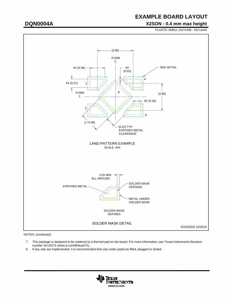
EXAMPLE BOARD LAYOUT
DQN0004AX2SON - 0.4 mm max height
PLASTIC SMALL OUTLINE - NO LEAD
4215302/E 12/2016
NOTES: (continued)
7. This package is designed to be soldered to a thermal pad on the board. For more information, see Texas Instruments literature
number SLUA271 (www.ti.com/lit/slua271) .8. If any vias are implemented, it is recommended that vias under paste be filled, plugged or tented.
www.ti.com
SOLDER MASK
DEFINED
SOLDER MASK DETAIL
0.05 MIN
ALL AROUND
SOLDER MASK
OPENING
METAL UNDER
SOLDER MASK
LAND PATTERN EXAMPLE
SCALE: 40X
SYMM
SYMM
1
2
3
4
4X (0.21)
4X (0.36)
(0.65)
(0.86)
( 0.48)
SEE DETAIL
4X (0.18)
(0.22) TYP
EXPOSED METAL
CLEARANCE
4X
(0.03)
EXPOSED METAL
5
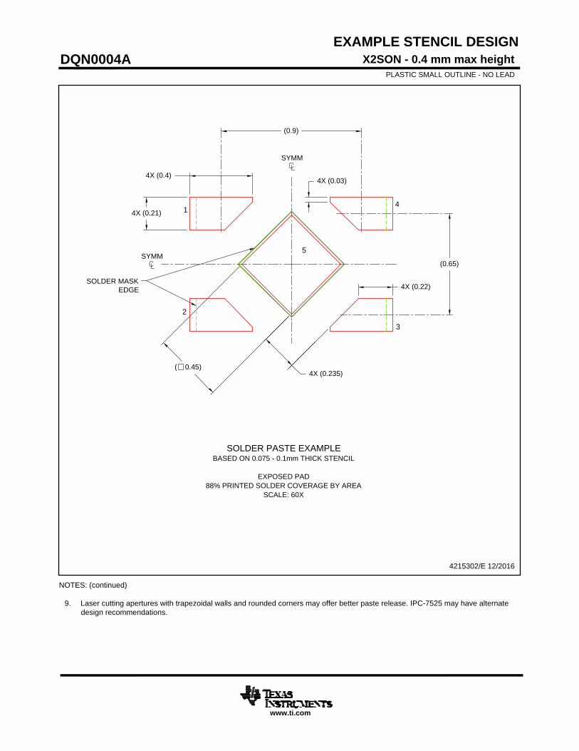
EXAMPLE STENCIL DESIGN
DQN0004AX2SON - 0.4 mm max height
PLASTIC SMALL OUTLINE - NO LEAD
4215302/E 12/2016
NOTES: (continued)
9. Laser cutting apertures with trapezoidal walls and rounded corners may offer better paste release. IPC-7525 may have alternate
design recommendations.
www.ti.com
SOLDER PASTE EXAMPLE
BASED ON 0.075 - 0.1mm THICK STENCIL
EXPOSED PAD
88% PRINTED SOLDER COVERAGE BY AREA
SCALE: 60X
SYMM
SYMM
1
2
3
4
SOLDER MASK
EDGE
4X (0.21)
4X (0.4)
(0.65)
(0.9)
( 0.45)
4X (0.03)
4X (0.235)
4X (0.22)
5
www.ti.com
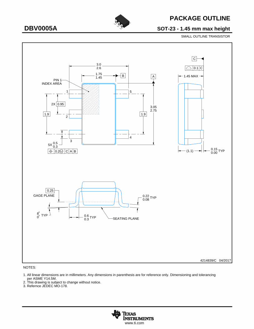
PACKAGE OUTLINE
C
TYP0.220.08
0.25
3.02.6
2X 0.95
1.9
1.45 MAX
TYP0.150.00
5X 0.50.3
TYP0.60.3
TYP80
1.9
A
3.052.75
B1.751.45
(1.1)
SOT-23 - 1.45 mm max heightDBV0005ASMALL OUTLINE TRANSISTOR
4214839/C 04/2017
NOTES: 1. All linear dimensions are in millimeters. Any dimensions in parenthesis are for reference only. Dimensioning and tolerancing per ASME Y14.5M.2. This drawing is subject to change without notice.3. Refernce JEDEC MO-178.
0.2 C A B
1
34
5
2
INDEX AREAPIN 1
GAGE PLANE
SEATING PLANE
0.1 C
SCALE 4.000
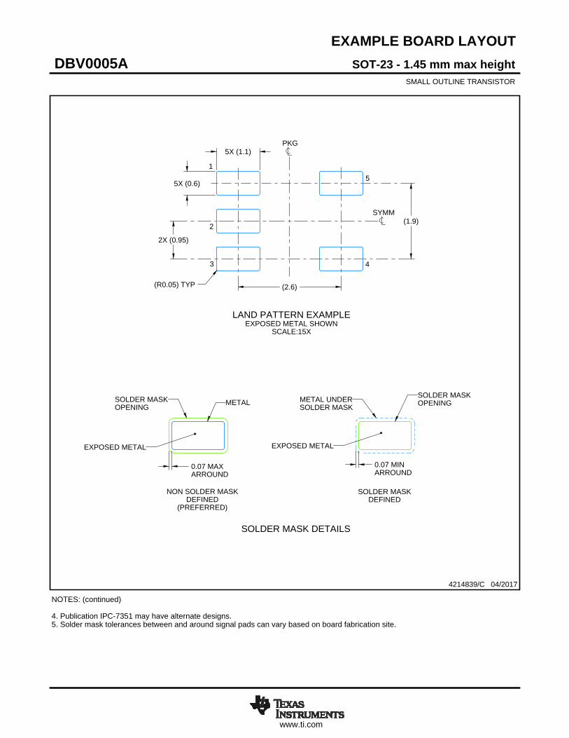
www.ti.com
EXAMPLE BOARD LAYOUT
0.07 MAXARROUND
0.07 MINARROUND
5X (1.1)
5X (0.6)
(2.6)
(1.9)
2X (0.95)
(R0.05) TYP
4214839/C 04/2017
SOT-23 - 1.45 mm max heightDBV0005ASMALL OUTLINE TRANSISTOR
NOTES: (continued) 4. Publication IPC-7351 may have alternate designs. 5. Solder mask tolerances between and around signal pads can vary based on board fabrication site.
SYMM
LAND PATTERN EXAMPLEEXPOSED METAL SHOWN
SCALE:15X
PKG
1
3 4
5
2
SOLDER MASKOPENINGMETAL UNDER
SOLDER MASK
SOLDER MASKDEFINED
EXPOSED METAL
METALSOLDER MASKOPENING
NON SOLDER MASKDEFINED
(PREFERRED)
SOLDER MASK DETAILS
EXPOSED METAL
www.ti.com
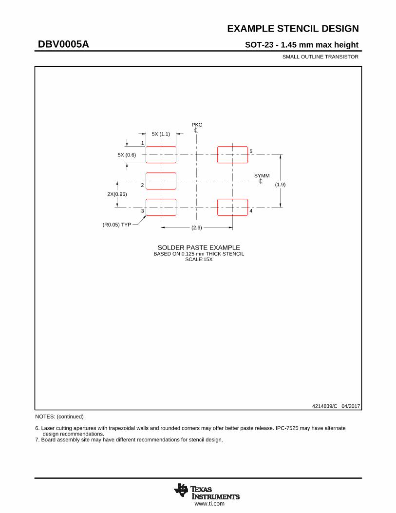
EXAMPLE STENCIL DESIGN
(2.6)
(1.9)
2X(0.95)
5X (1.1)
5X (0.6)
(R0.05) TYP
SOT-23 - 1.45 mm max heightDBV0005ASMALL OUTLINE TRANSISTOR
4214839/C 04/2017
NOTES: (continued) 6. Laser cutting apertures with trapezoidal walls and rounded corners may offer better paste release. IPC-7525 may have alternate design recommendations. 7. Board assembly site may have different recommendations for stencil design.
SOLDER PASTE EXAMPLEBASED ON 0.125 mm THICK STENCIL
SCALE:15X
SYMM
PKG
1
3 4
5
2
IMPORTANT NOTICE
Texas Instruments Incorporated (TI) reserves the right to make corrections, enhancements, improvements and other changes to itssemiconductor products and services per JESD46, latest issue, and to discontinue any product or service per JESD48, latest issue. Buyersshould obtain the latest relevant information before placing orders and should verify that such information is current and complete.TI’s published terms of sale for semiconductor products (http://www.ti.com/sc/docs/stdterms.htm) apply to the sale of packaged integratedcircuit products that TI has qualified and released to market. Additional terms may apply to the use or sale of other types of TI products andservices.Reproduction of significant portions of TI information in TI data sheets is permissible only if reproduction is without alteration and isaccompanied by all associated warranties, conditions, limitations, and notices. TI is not responsible or liable for such reproduceddocumentation. Information of third parties may be subject to additional restrictions. Resale of TI products or services with statementsdifferent from or beyond the parameters stated by TI for that product or service voids all express and any implied warranties for theassociated TI product or service and is an unfair and deceptive business practice. TI is not responsible or liable for any such statements.Buyers and others who are developing systems that incorporate TI products (collectively, “Designers”) understand and agree that Designersremain responsible for using their independent analysis, evaluation and judgment in designing their applications and that Designers havefull and exclusive responsibility to assure the safety of Designers' applications and compliance of their applications (and of all TI productsused in or for Designers’ applications) with all applicable regulations, laws and other applicable requirements. Designer represents that, withrespect to their applications, Designer has all the necessary expertise to create and implement safeguards that (1) anticipate dangerousconsequences of failures, (2) monitor failures and their consequences, and (3) lessen the likelihood of failures that might cause harm andtake appropriate actions. Designer agrees that prior to using or distributing any applications that include TI products, Designer willthoroughly test such applications and the functionality of such TI products as used in such applications.TI’s provision of technical, application or other design advice, quality characterization, reliability data or other services or information,including, but not limited to, reference designs and materials relating to evaluation modules, (collectively, “TI Resources”) are intended toassist designers who are developing applications that incorporate TI products; by downloading, accessing or using TI Resources in anyway, Designer (individually or, if Designer is acting on behalf of a company, Designer’s company) agrees to use any particular TI Resourcesolely for this purpose and subject to the terms of this Notice.TI’s provision of TI Resources does not expand or otherwise alter TI’s applicable published warranties or warranty disclaimers for TIproducts, and no additional obligations or liabilities arise from TI providing such TI Resources. TI reserves the right to make corrections,enhancements, improvements and other changes to its TI Resources. TI has not conducted any testing other than that specificallydescribed in the published documentation for a particular TI Resource.Designer is authorized to use, copy and modify any individual TI Resource only in connection with the development of applications thatinclude the TI product(s) identified in such TI Resource. NO OTHER LICENSE, EXPRESS OR IMPLIED, BY ESTOPPEL OR OTHERWISETO ANY OTHER TI INTELLECTUAL PROPERTY RIGHT, AND NO LICENSE TO ANY TECHNOLOGY OR INTELLECTUAL PROPERTYRIGHT OF TI OR ANY THIRD PARTY IS GRANTED HEREIN, including but not limited to any patent right, copyright, mask work right, orother intellectual property right relating to any combination, machine, or process in which TI products or services are used. Informationregarding or referencing third-party products or services does not constitute a license to use such products or services, or a warranty orendorsement thereof. Use of TI Resources may require a license from a third party under the patents or other intellectual property of thethird party, or a license from TI under the patents or other intellectual property of TI.TI RESOURCES ARE PROVIDED “AS IS” AND WITH ALL FAULTS. TI DISCLAIMS ALL OTHER WARRANTIES ORREPRESENTATIONS, EXPRESS OR IMPLIED, REGARDING RESOURCES OR USE THEREOF, INCLUDING BUT NOT LIMITED TOACCURACY OR COMPLETENESS, TITLE, ANY EPIDEMIC FAILURE WARRANTY AND ANY IMPLIED WARRANTIES OFMERCHANTABILITY, FITNESS FOR A PARTICULAR PURPOSE, AND NON-INFRINGEMENT OF ANY THIRD PARTY INTELLECTUALPROPERTY RIGHTS. TI SHALL NOT BE LIABLE FOR AND SHALL NOT DEFEND OR INDEMNIFY DESIGNER AGAINST ANY CLAIM,INCLUDING BUT NOT LIMITED TO ANY INFRINGEMENT CLAIM THAT RELATES TO OR IS BASED ON ANY COMBINATION OFPRODUCTS EVEN IF DESCRIBED IN TI RESOURCES OR OTHERWISE. IN NO EVENT SHALL TI BE LIABLE FOR ANY ACTUAL,DIRECT, SPECIAL, COLLATERAL, INDIRECT, PUNITIVE, INCIDENTAL, CONSEQUENTIAL OR EXEMPLARY DAMAGES INCONNECTION WITH OR ARISING OUT OF TI RESOURCES OR USE THEREOF, AND REGARDLESS OF WHETHER TI HAS BEENADVISED OF THE POSSIBILITY OF SUCH DAMAGES.Unless TI has explicitly designated an individual product as meeting the requirements of a particular industry standard (e.g., ISO/TS 16949and ISO 26262), TI is not responsible for any failure to meet such industry standard requirements.Where TI specifically promotes products as facilitating functional safety or as compliant with industry functional safety standards, suchproducts are intended to help enable customers to design and create their own applications that meet applicable functional safety standardsand requirements. Using products in an application does not by itself establish any safety features in the application. Designers mustensure compliance with safety-related requirements and standards applicable to their applications. Designer may not use any TI products inlife-critical medical equipment unless authorized officers of the parties have executed a special contract specifically governing such use.Life-critical medical equipment is medical equipment where failure of such equipment would cause serious bodily injury or death (e.g., lifesupport, pacemakers, defibrillators, heart pumps, neurostimulators, and implantables). Such equipment includes, without limitation, allmedical devices identified by the U.S. Food and Drug Administration as Class III devices and equivalent classifications outside the U.S.TI may expressly designate certain products as completing a particular qualification (e.g., Q100, Military Grade, or Enhanced Product).Designers agree that it has the necessary expertise to select the product with the appropriate qualification designation for their applicationsand that proper product selection is at Designers’ own risk. Designers are solely responsible for compliance with all legal and regulatoryrequirements in connection with such selection.Designer will fully indemnify TI and its representatives against any damages, costs, losses, and/or liabilities arising out of Designer’s non-compliance with the terms and provisions of this Notice.
Mailing Address: Texas Instruments, Post Office Box 655303, Dallas, Texas 75265Copyright © 2018, Texas Instruments Incorporated