Embed Size (px)
Citation preview
DA6510.009
6 September, 2018
. 1 (32)
MAS6510 Capacitive Sensor Signal Interface IC
• Single or Dual Capacitance Sensors
• Very Low Power Consumption
• On Chip Temperature Sensor
• VDD Level Monitoring
• 24-Bit Ratiometric CDC
• EEPROM Calibration Memory
• SPI or I2C Bus with programmable I2C device address
DESCRIPTION MAS6510 capacitive sensor signal Interface IC can interface both single and dual capacitance sensors.
It uses a 24-bit Capacitance-to-Digital Converter (CDC), which employs a delta-sigma (ΔΣ) conversion technique. The output data from the high order ΔΣ-modulator is processed by an on-chip decimator filter, producing a high resolution conversion result. The converter is run by an internal clock oscillator making an external converter clock unnecessary.
The converter input range is programmable to meet various sensor offset and changing capacitance values. At normal clock frequency maximum sensor capacitance is 20pF but up to 160pF value can be reached by using available clock division options.
The measurement resolution depends on the programmed capacitance range and over sampling ratio (OSR) selections.
MAS6510 supports two capacitance measurement modes. The output can be proportional either to
capacitance difference (CS-CR) or to capacitance ratio (CS-CR)/CS.
The IC is designed especially to meet the requirement for low power consumption, thus making it an ideal choice for battery powered systems. Current consumption values of 50.3 µA with high resolution or 3.5 µA with low resolution, at a conversion rate of one conversion per second, can be achieved.
In addition to measuring capacitance the device has an internal temperature sensor for temperature measurement and temperature compensation purposes. The VDD level monitoring feature is useful especially in battery operated systems. The 256-bit EEPROM memory stores trimming and calibration coefficients on chip.
A serial interface, compatible with a bi-directional 2-wire I2C bus and 4-wire SPI bus, is used for conversion setup, starting a conversion and reading the conversion result.
FEATURES APPLICATIONS
• Sensor Offset and Gain Adjustment
• Changing Capacitance Range C 2pF…30pF
• Internal Offset Capacitance Matrix 0pF…22pF
• External Capacitance up to 160pF
• Resolution 17.5 bit
• Internal Clock Oscillator
• On Chip Temperature Sensor -40C...+85C
• VDD Level Monitoring
• Low Voltage Operation 1.8 V/1.9V…3.6 V
• Low Supply Current: 3.5 µA...50.3 µA
• Conversion Time 5.8ms...82.6ms (12Hz...173Hz)
• Internal 256-bit EEPROM Calibration Memory
• Internal Clock Oscillator
• I2C and SPI Compatible Serial Interface
• QFN-16 Package
• Capacitive Pressure Sensors
• Humidity Sensors
• Medical Devices
• Flow Meters
• Sport Watches
• Altimeter and Barometer Systems
• Mobile and Battery Powered Systems
• Low Frequency Measurement applications
• Current/Power Consumption Critical Systems
• Industrial and Process Control applications in noisy environments
DA6510.009
6 September, 2018
. 2 (32)
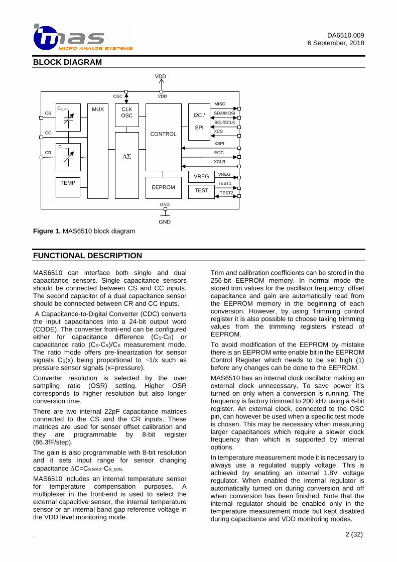
BLOCK DIAGRAM
Figure 1. MAS6510 block diagram
FUNCTIONAL DESCRIPTION MAS6510 can interface both single and dual capacitance sensors. Single capacitance sensors should be connected between CS and CC inputs. The second capacitor of a dual capacitance sensor should be connected between CR and CC inputs.
A Capacitance-to-Digital Converter (CDC) converts the input capacitances into a 24-bit output word (CODE). The converter front-end can be configured either for capacitance difference (CS-CR) or capacitance ratio (CS-CR)/CS measurement mode. The ratio mode offers pre-linearization for sensor signals CS(x) being proportional to ~1/x such as pressure sensor signals (x=pressure).
Converter resolution is selected by the over sampling ratio (OSR) setting. Higher OSR corresponds to higher resolution but also longer conversion time.
There are two internal 22pF capacitance matrices connected to the CS and the CR inputs. These matrices are used for sensor offset calibration and they are programmable by 8-bit register (86.3fF/step).
The gain is also programmable with 8-bit resolution and it sets input range for sensor changing
capacitance C=CS MAX-CS_MIN.
MAS6510 includes an internal temperature sensor for temperature compensation purposes. A multiplexer in the front-end is used to select the external capacitive sensor, the internal temperature sensor or an internal band gap reference voltage in the VDD level monitoring mode.
Trim and calibration coefficients can be stored in the 256-bit EEPROM memory. In normal mode the stored trim values for the oscillator frequency, offset capacitance and gain are automatically read from the EEPROM memory in the beginning of each conversion. However, by using Trimming control register it is also possible to choose taking trimming values from the trimming registers instead of EEPROM.
To avoid modification of the EEPROM by mistake there is an EEPROM write enable bit in the EEPROM Control Register which needs to be set high (1) before any changes can be done to the EEPROM.
MAS6510 has an internal clock oscillator making an external clock unnecessary. To save power it’s turned on only when a conversion is running. The frequency is factory trimmed to 200 kHz using a 6-bit register. An external clock, connected to the OSC pin, can however be used when a specific test mode is chosen. This may be necessary when measuring larger capacitances which require a slower clock frequency than which is supported by internal options.
In temperature measurement mode it is necessary to always use a regulated supply voltage. This is achieved by enabling an internal 1.8V voltage regulator. When enabled the internal regulator is automatically turned on during conversion and off when conversion has been finished. Note that the internal regulator should be enabled only in the temperature measurement mode but kept disabled during capacitance and VDD monitoring modes.
MISO
SDA/MOSI
SCL/SCLK
MUX
TEMP
CONTROL
I2C /
SPI
EEPROM
CLK OSC
XCS
XSPI
EOC
XCLR
CS
CC
CR
VDD
GND
GND
VREG
TEST
VREG
TEST1
TEST2
VDD
OSC
CS_INT
CR_INT
DA6510.009
6 September, 2018
3 (32)
FUNCTIONAL DESCRIPTION In battery operated applications the VDD of the MAS6510 can vary along with battery capacity. In such case the VDD level monitoring feature can be useful to indicate battery level, help choosing between different power modes in the system or even using measured VDD level for compensating VDD dependencies. In the VDD level monitoring mode the on-chip regulator has to be disabled.
Communication with MAS6510 is handled by the serial interface compatible with either a bi-directional 2-wire I2C bus or a 4-wire SPI bus. The XSPI pin is for selecting which bus type is used.
Note: The 2-wire I2C bus of MAS6510 supports only basic I2C bus communication protocol but not for example 10-bit addressing, arbitration and clock stretching features of the I2C bus specification.
The XCLR pin can be used to hard reset the device including the serial communication. Device reset is possible also via serial bus using the reset register.
Connecting VDD triggers internal power on reset (POR) circuit which resets the device.
Despite of on chip power on reset (POR) circuit it is recommended to reset the device manually after every power up to guarantee proper register settings after any VDD rise conditions.
The EOC pin indicates if a conversion has finished and the result is ready to be read from the memory via the serial interface. Using the EOC signal is not necessary since it is alternatively possible to wait at least maximum conversion time period before reading out the result.
ABSOLUTE MAXIMUM RATINGS
All Voltages with Respect to Ground
Parameter Symbol Conditions Min Max Unit
Supply Voltage VDD -0.3 5.0 V
Voltage Range for All Pins -0.3 VDD + 0.3 V
Latch-Up Current Limit ILU For all pins, test according to JESD78A.
-100 +100 mA
Junction Temperature TJmax + 150 °C
Storage Temperature TS Note 1 - 55 +125 °C
ESD Rating
VHBM Note 2 ±1 kV
VCDM Note 3 ±500V V
Note: The absolute maximum rating values are stress ratings only. Functional operation of the device at conditions between maximum operating conditions and absolute maximum ratings is not implied and EEPROM contents may be corrupted. Exposure to these conditions for extended periods may affect device reliability (e.g. hot carrier degradation, oxide breakdown). Applying conditions above absolute maximum ratings may be destructive to the devices. Note: This is a CMOS device and therefore it should be handled carefully to avoid any damage by static voltages (ESD). Note 1: See EEPROM memory data retention at hot temperature. Storage or bake at hot temperatures will reduce wafer level trimming and calibration data retention time. Note 2: JEDEC document JEP155 states that 500V HBM allows safe manufacturing with a standard ESD control process. Note 3: JEDEC document JEP157 states that 250V CDM allows safe manufacturing with a standard ESD control process.
RECOMMENDED OPERATION CONDITIONS
Parameter Symbol Conditions Min Typ Max Unit
Supply Voltage VDD Capacitance and VDD level monitoring modes Note 1
1.8 2.7 3.6 V
Temperature mode Note 1
1.9 2.7 3.6 V
Operating Temperature TA -40 +25 +85 °C
EEPROM Write Temperature
TA Note 2 +10 +25 +40 °C
Note 1. In capacitance measurement and VDD level monitoring the regulator must be disabled (TEMPREGEN=0) which allows operation down to 1.8V. In temperature measurement the typ 1.8V regulator has to be enabled (TEMPREGEN=1) which limits the minimum supply voltage down to 1.9V. Note 2: EEPROM write operation is recommended to be done at room temperature
DA6510.009
6 September, 2018
4 (32)
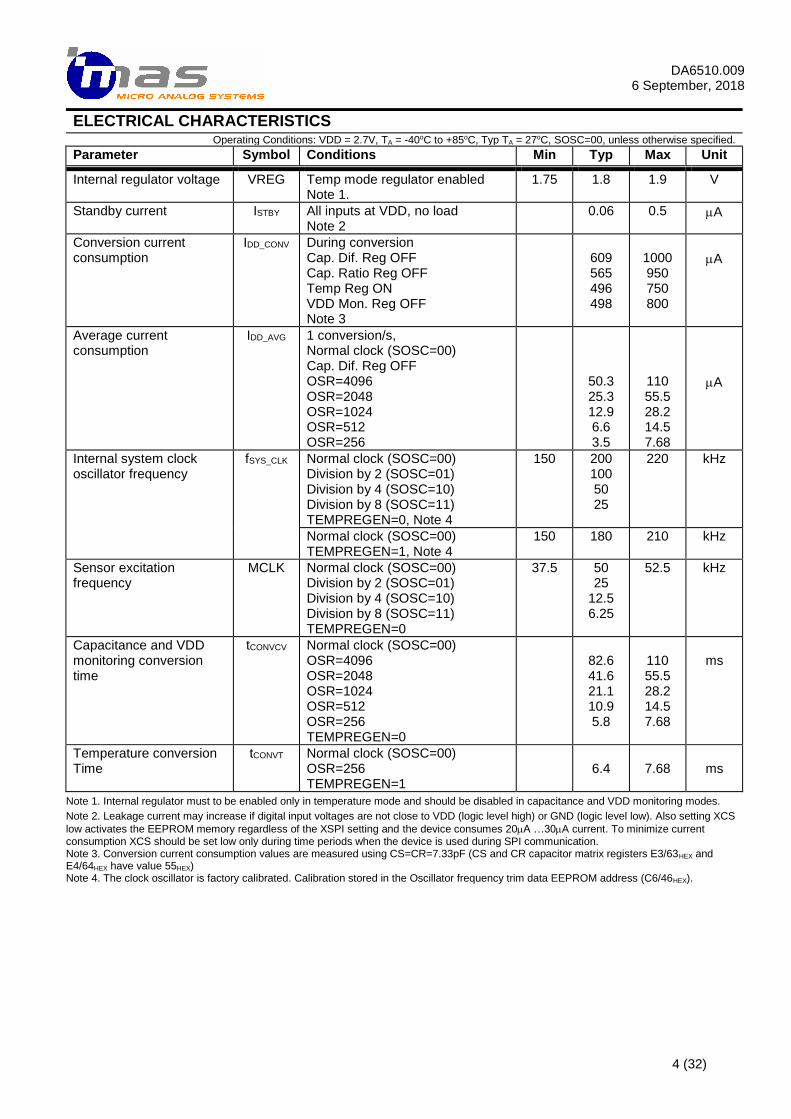
ELECTRICAL CHARACTERISTICS Operating Conditions: VDD = 2.7V, TA = -40oC to +85oC, Typ TA = 27oC, SOSC=00, unless otherwise specified.
Parameter Symbol Conditions Min Typ Max Unit
Internal regulator voltage VREG Temp mode regulator enabled Note 1.
1.75 1.8 1.9 V
Standby current ISTBY All inputs at VDD, no load Note 2
0.06 0.5 A
Conversion current consumption
IDD_CONV During conversion Cap. Dif. Reg OFF Cap. Ratio Reg OFF Temp Reg ON VDD Mon. Reg OFF Note 3
609 565 496 498
1000 950 750 800
A
Average current consumption
IDD_AVG 1 conversion/s, Normal clock (SOSC=00) Cap. Dif. Reg OFF OSR=4096 OSR=2048 OSR=1024 OSR=512 OSR=256
50.3 25.3 12.9 6.6 3.5
110 55.5 28.2 14.5 7.68
A
Internal system clock oscillator frequency
fSYS_CLK Normal clock (SOSC=00) Division by 2 (SOSC=01) Division by 4 (SOSC=10) Division by 8 (SOSC=11) TEMPREGEN=0, Note 4
150
200 100 50 25
220
kHz
Normal clock (SOSC=00) TEMPREGEN=1, Note 4
150
180 210
kHz
Sensor excitation frequency
MCLK Normal clock (SOSC=00) Division by 2 (SOSC=01) Division by 4 (SOSC=10) Division by 8 (SOSC=11) TEMPREGEN=0
37.5 50 25
12.5 6.25
52.5 kHz
Capacitance and VDD monitoring conversion time
tCONVCV Normal clock (SOSC=00) OSR=4096 OSR=2048 OSR=1024 OSR=512 OSR=256 TEMPREGEN=0
82.6 41.6 21.1 10.9 5.8
110 55.5 28.2 14.5 7.68
ms
Temperature conversion Time
tCONVT Normal clock (SOSC=00) OSR=256 TEMPREGEN=1
6.4
7.68
ms
Note 1. Internal regulator must to be enabled only in temperature mode and should be disabled in capacitance and VDD monitoring modes.
Note 2. Leakage current may increase if digital input voltages are not close to VDD (logic level high) or GND (logic level low). Also setting XCS
low activates the EEPROM memory regardless of the XSPI setting and the device consumes 20A …30A current. To minimize current consumption XCS should be set low only during time periods when the device is used during SPI communication. Note 3. Conversion current consumption values are measured using CS=CR=7.33pF (CS and CR capacitor matrix registers E3/63HEX and E4/64HEX have value 55HEX) Note 4. The clock oscillator is factory calibrated. Calibration stored in the Oscillator frequency trim data EEPROM address (C6/46HEX).
DA6510.009
6 September, 2018
5 (32)
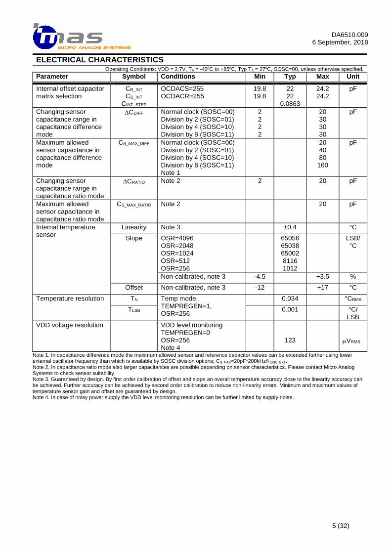
ELECTRICAL CHARACTERISTICS Operating Conditions: VDD = 2.7V, TA = -40oC to +85oC, Typ TA = 27oC, SOSC=00, unless otherwise specified.
Parameter Symbol Conditions Min Typ Max Unit
Internal offset capacitor matrix selection
CR_INT CS_INT
CINT_STEP
OCDACS=255 OCDACR=255
19.8 19.8
22 22
0.0863
24.2 24.2
pF
Changing sensor capacitance range in capacitance difference mode
CDIFF Normal clock (SOSC=00) Division by 2 (SOSC=01) Division by 4 (SOSC=10) Division by 8 (SOSC=11)
2 2 2 2
20 30 30 30
pF
Maximum allowed sensor capacitance in capacitance difference mode
CS_MAX_DIFF Normal clock (SOSC=00) Division by 2 (SOSC=01) Division by 4 (SOSC=10) Division by 8 (SOSC=11) Note 1
20 40 80 160
pF
Changing sensor capacitance range in capacitance ratio mode
CRATIO Note 2 2 20 pF
Maximum allowed sensor capacitance in capacitance ratio mode
CS_MAX_RATIO Note 2
20
pF
Internal temperature sensor
Linearity Note 3 ±0.4 °C
Slope
OSR=4096 OSR=2048 OSR=1024 OSR=512 OSR=256
65056 65038 65002 8116 1012
LSB/ °C
Non-calibrated, note 3 -4.5 +3.5 %
Offset Non-calibrated, note 3 -12 +17 °C
Temperature resolution
TN Temp mode, TEMPREGEN=1, OSR=256
0.034 °CRMS
TLSB 0.001 °C/ LSB
VDD voltage resolution
VDD level monitoring TEMPREGEN=0 OSR=256 Note 4
123
VRMS
Note 1. In capacitance difference mode the maximum allowed sensor and reference capacitor values can be extended further using lower external oscillator frequency than which is available by SOSC division options; CS_MAX=20pF*200kHz/f OSC_EXT. Note 2. In capacitance ratio mode also larger capacitances are possible depending on sensor characteristics. Please contact Micro Analog Systems to check sensor suitability. Note 3. Guaranteed by design. By first order calibration of offset and slope an overall temperature accuracy close to the linearity accuracy can be achieved. Further accuracy can be achieved by second order calibration to reduce non-linearity errors. Minimum and maximum values of temperature sensor gain and offset are guaranteed by design. Note 4. In case of noisy power supply the VDD level monitoring resolution can be further limited by supply noise.
DA6510.009
6 September, 2018
6 (32)
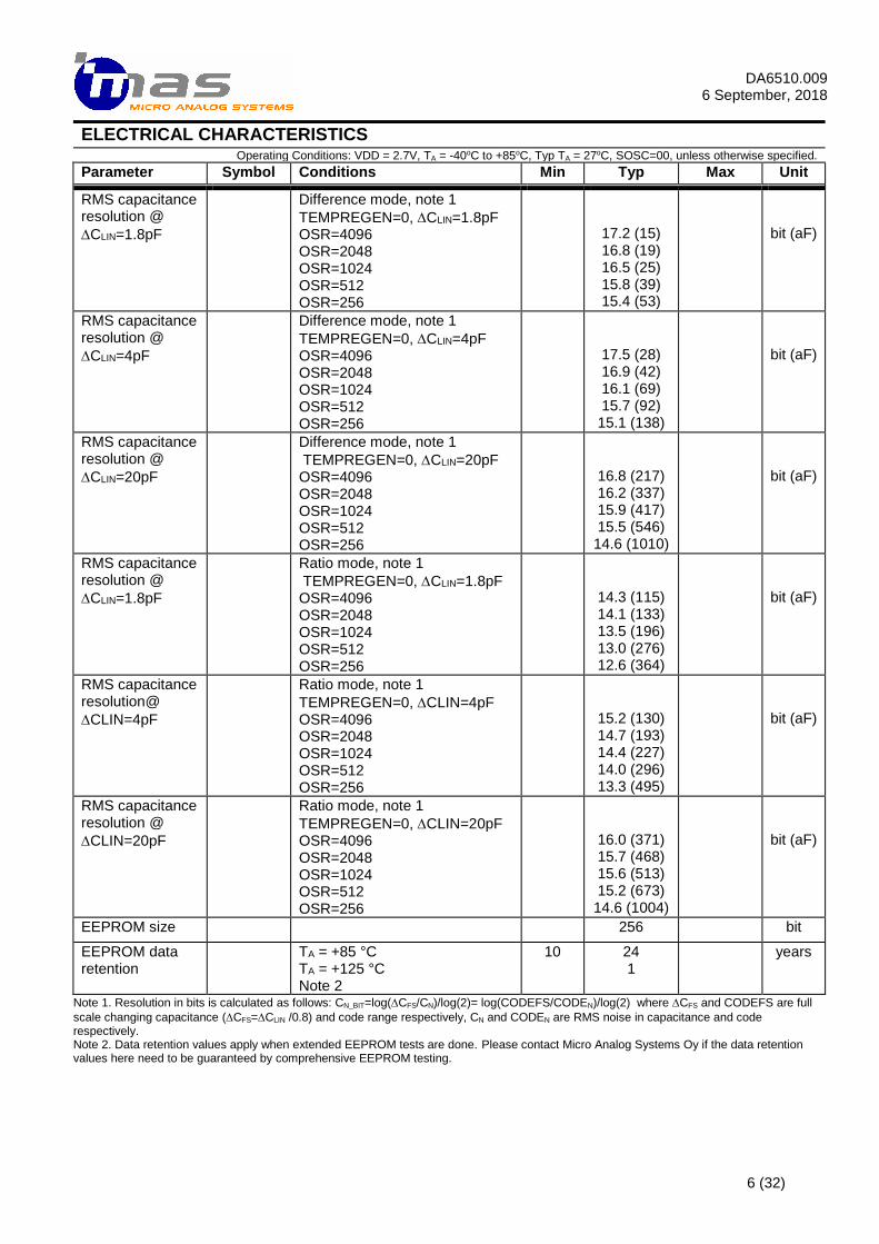
ELECTRICAL CHARACTERISTICS Operating Conditions: VDD = 2.7V, TA = -40oC to +85oC, Typ TA = 27oC, SOSC=00, unless otherwise specified.
Parameter Symbol Conditions Min Typ Max Unit
RMS capacitance resolution @
CLIN=1.8pF
Difference mode, note 1
TEMPREGEN=0, CLIN=1.8pF OSR=4096 OSR=2048 OSR=1024 OSR=512 OSR=256
17.2 (15) 16.8 (19) 16.5 (25) 15.8 (39) 15.4 (53)
bit (aF)
RMS capacitance resolution @
CLIN=4pF
Difference mode, note 1
TEMPREGEN=0, CLIN=4pF OSR=4096 OSR=2048 OSR=1024 OSR=512 OSR=256
17.5 (28) 16.9 (42) 16.1 (69) 15.7 (92) 15.1 (138)
bit (aF)
RMS capacitance resolution @
CLIN=20pF
Difference mode, note 1
TEMPREGEN=0, CLIN=20pF OSR=4096 OSR=2048 OSR=1024 OSR=512 OSR=256
16.8 (217) 16.2 (337) 15.9 (417) 15.5 (546) 14.6 (1010)
bit (aF)
RMS capacitance resolution @
CLIN=1.8pF
Ratio mode, note 1
TEMPREGEN=0, CLIN=1.8pF OSR=4096 OSR=2048 OSR=1024 OSR=512 OSR=256
14.3 (115) 14.1 (133) 13.5 (196) 13.0 (276) 12.6 (364)
bit (aF)
RMS capacitance resolution@
CLIN=4pF
Ratio mode, note 1
TEMPREGEN=0, CLIN=4pF OSR=4096 OSR=2048 OSR=1024 OSR=512 OSR=256
15.2 (130) 14.7 (193) 14.4 (227) 14.0 (296) 13.3 (495)
bit (aF)
RMS capacitance resolution @
CLIN=20pF
Ratio mode, note 1
TEMPREGEN=0, CLIN=20pF OSR=4096 OSR=2048 OSR=1024 OSR=512 OSR=256
16.0 (371) 15.7 (468) 15.6 (513) 15.2 (673) 14.6 (1004)
bit (aF)
EEPROM size 256 bit
EEPROM data retention
TA = +85 °C TA = +125 °C Note 2
10 24 1
years
Note 1. Resolution in bits is calculated as follows: CN_BIT=log(CFS/CN)/log(2)= log(CODEFS/CODEN)/log(2) where CFS and CODEFS are full
scale changing capacitance (CFS=CLIN /0.8) and code range respectively, CN and CODEN are RMS noise in capacitance and code respectively. Note 2. Data retention values apply when extended EEPROM tests are done. Please contact Micro Analog Systems Oy if the data retention values here need to be guaranteed by comprehensive EEPROM testing.
DA6510.009
6 September, 2018
7 (32)
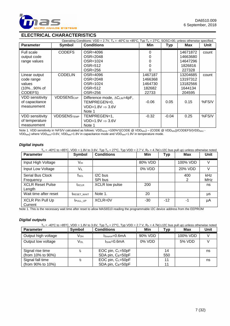
ELECTRICAL CHARACTERISTICS Operating Conditions: VDD = 2.7V, TA = -40oC to +85oC, Typ TA = 27oC, SOSC=00, unless otherwise specified.
Parameter Symbol Conditions Min Typ Max Unit
Full scale output code range values
CODEFS OSR=4096 OSR=2048 OSR=1024 OSR=512 OSR=256
0 0 0 0 0
14671872 14663680 14647296 1826816 227328
count
Linear output code range values (10%...90% of CODEFS)
CODELIN OSR=4096 OSR=2048 OSR=1024 OSR=512 OSR=256
1467187 1466368 1464730 182682 22733
13204685 13197312 13182566 1644134 204595
count
VDD sensitivity of capacitance measurement
VDDSENSCAP Difference mode, CLIN=4pF, TEMPREGEN=0,
VDD=1.8V 3.6V Note 1
-0.06
0.05
0.15
%FS/V
VDD sensitivity of temperature measurement
VDDSENSTEMP TEMPREGEN=1,
VDD=1.9V 3.6V Note 1
-0.32 -0.04 0.25 %FS/V
Note 1. VDD sensitivity in %FS/V calculated as follows: VDDSENS =100%*((CODE @ VDDMAX) – (CODE @ VDDMIN))/CODEFS/(VDDMAX - VDDMIN) where VDDMAX=3.6V, VDDMIN=1.8V in capacitance mode and VDDMIN=1.9V in temperature mode.
Digital inputs
TA = -40oC to +85oC, VDD = 1.8V to 3.6V, Typ TA = 27oC, Typ VDD = 2.7 V, RP = 4.7k (I2C bus pull up) unless otherwise noted
Parameter Symbol Conditions Min Typ Max Unit
Input High Voltage VIH 80% VDD 100% VDD V
Input Low Voltage VIL 0% VDD 20% VDD V
Serial Bus Clock Frequency
fSCL I2C bus SPI bus
400 2
kHz MHz
XCLR Reset Pulse Length
tXCLR XCLR low pulse 200 ns
Wait time after reset tRESET_WAIT Note 1. 20 µs
XCLR Pin Pull Up Current
IPULL_UP XCLR=0V
-30 -12 -1 µA
Note 1. This is the necessary wait time after reset to allow MAS6510 reading the programmable I2C device address from the EEPROM
Digital outputs
TA = -40oC to +85oC, VDD = 1.8V to 3.6V, Typ TA = 27oC, Typ VDD = 2.7 V, RP = 4.7k (I2C bus pull up) unless otherwise noted
Parameter Symbol Conditions Min Typ Max Unit
Output high voltage VOH ISource=0.6mA 90% VDD 100% VDD V
Output low voltage
VOL ISink=0.6mA 0% VDD 5% VDD V
Signal rise time (from 10% to 90%)
tr EOC pin, CL=50pF SDA pin, CB=50pF
14 550
ns
Signal fall time (from 90% to 10%)
tf EOC pin, CL=50pF SDA pin, CB=50pF
11 11
ns
DA6510.009
6 September, 2018
8 (32)
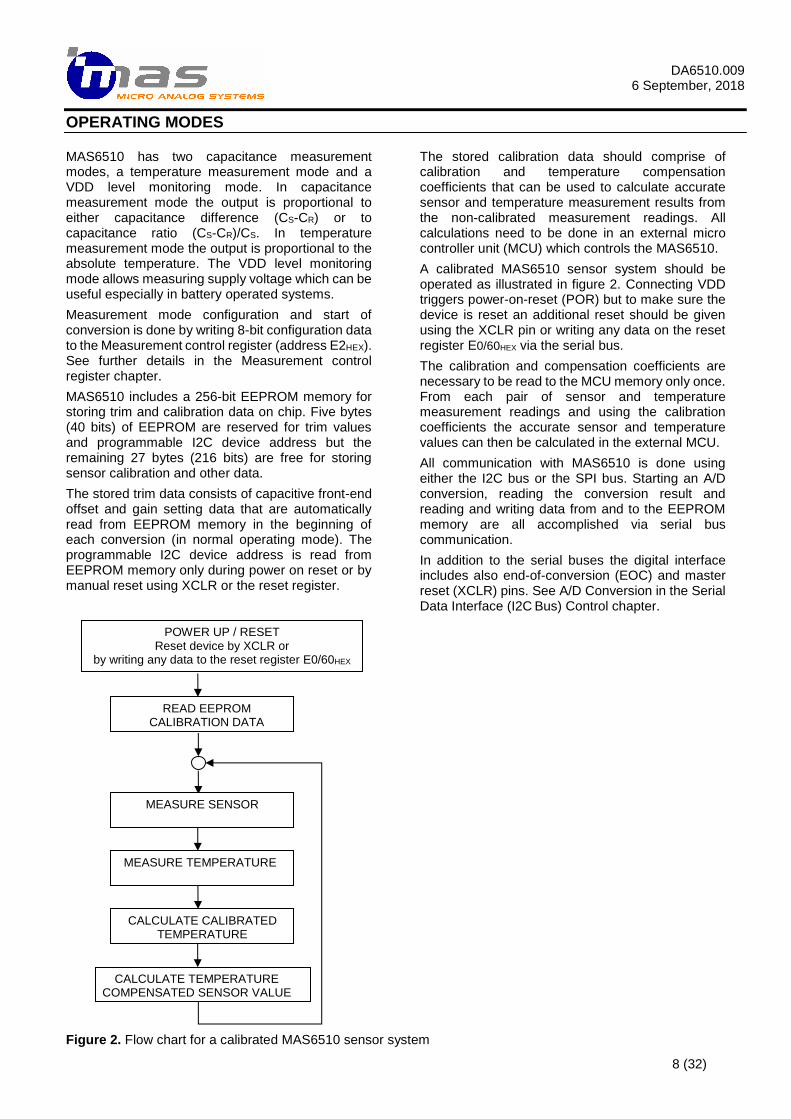
OPERATING MODES MAS6510 has two capacitance measurement modes, a temperature measurement mode and a VDD level monitoring mode. In capacitance measurement mode the output is proportional to either capacitance difference (CS-CR) or to capacitance ratio (CS-CR)/CS. In temperature measurement mode the output is proportional to the absolute temperature. The VDD level monitoring mode allows measuring supply voltage which can be useful especially in battery operated systems.
Measurement mode configuration and start of conversion is done by writing 8-bit configuration data to the Measurement control register (address E2HEX). See further details in the Measurement control register chapter.
MAS6510 includes a 256-bit EEPROM memory for storing trim and calibration data on chip. Five bytes (40 bits) of EEPROM are reserved for trim values and programmable I2C device address but the remaining 27 bytes (216 bits) are free for storing sensor calibration and other data.
The stored trim data consists of capacitive front-end offset and gain setting data that are automatically read from EEPROM memory in the beginning of each conversion (in normal operating mode). The programmable I2C device address is read from EEPROM memory only during power on reset or by manual reset using XCLR or the reset register.
The stored calibration data should comprise of calibration and temperature compensation coefficients that can be used to calculate accurate sensor and temperature measurement results from the non-calibrated measurement readings. All calculations need to be done in an external micro controller unit (MCU) which controls the MAS6510.
A calibrated MAS6510 sensor system should be operated as illustrated in figure 2. Connecting VDD triggers power-on-reset (POR) but to make sure the device is reset an additional reset should be given using the XCLR pin or writing any data on the reset register E0/60HEX via the serial bus.
The calibration and compensation coefficients are necessary to be read to the MCU memory only once. From each pair of sensor and temperature measurement readings and using the calibration coefficients the accurate sensor and temperature values can then be calculated in the external MCU.
All communication with MAS6510 is done using either the I2C bus or the SPI bus. Starting an A/D conversion, reading the conversion result and reading and writing data from and to the EEPROM memory are all accomplished via serial bus communication.
In addition to the serial buses the digital interface includes also end-of-conversion (EOC) and master reset (XCLR) pins. See A/D Conversion in the Serial Data Interface (I2C Bus) Control chapter.
Figure 2. Flow chart for a calibrated MAS6510 sensor system
POWER UP / RESET Reset device by XCLR or
by writing any data to the reset register E0/60HEX
READ EEPROM CALIBRATION DATA
MEASURE SENSOR
MEASURE TEMPERATURE
CALCULATE CALIBRATED TEMPERATURE
CALCULATE TEMPERATURE COMPENSATED SENSOR VALUE
DA6510.009
6 September, 2018
9 (32)
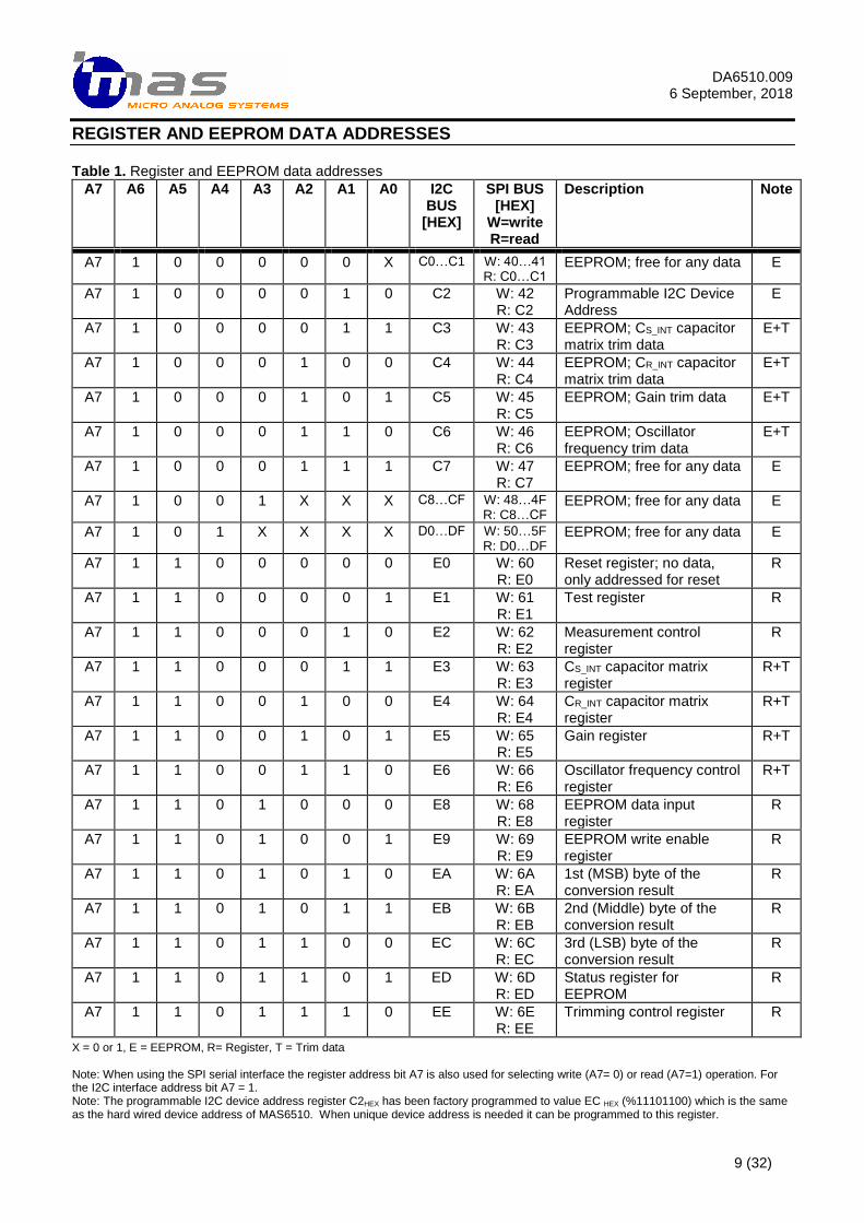
REGISTER AND EEPROM DATA ADDRESSES Table 1. Register and EEPROM data addresses
A7 A6 A5 A4 A3 A2 A1 A0 I2C BUS
[HEX]
SPI BUS [HEX]
W=write R=read
Description Note
A7 1 0 0 0 0 0 X C0…C1 W: 40…41 R: C0…C1
EEPROM; free for any data E
A7 1 0 0 0 0 1 0 C2 W: 42 R: C2
Programmable I2C Device Address
E
A7 1 0 0 0 0 1 1 C3 W: 43 R: C3
EEPROM; CS_INT capacitor matrix trim data
E+T
A7 1 0 0 0 1 0 0 C4 W: 44 R: C4
EEPROM; CR_INT capacitor matrix trim data
E+T
A7 1 0 0 0 1 0 1 C5 W: 45 R: C5
EEPROM; Gain trim data E+T
A7 1 0 0 0 1 1 0 C6 W: 46 R: C6
EEPROM; Oscillator frequency trim data
E+T
A7 1 0 0 0 1 1 1 C7 W: 47 R: C7
EEPROM; free for any data E
A7 1 0 0 1 X X X C8…CF W: 48…4F R: C8…CF
EEPROM; free for any data E
A7 1 0 1 X X X X D0…DF W: 50…5F R: D0…DF
EEPROM; free for any data E
A7 1 1 0 0 0 0 0 E0 W: 60 R: E0
Reset register; no data, only addressed for reset
R
A7 1 1 0 0 0 0 1 E1 W: 61 R: E1
Test register R
A7 1 1 0 0 0 1 0 E2 W: 62 R: E2
Measurement control register
R
A7 1 1 0 0 0 1 1 E3 W: 63 R: E3
CS_INT capacitor matrix register
R+T
A7 1 1 0 0 1 0 0 E4 W: 64 R: E4
CR_INT capacitor matrix register
R+T
A7 1 1 0 0 1 0 1 E5 W: 65 R: E5
Gain register R+T
A7 1 1 0 0 1 1 0 E6 W: 66 R: E6
Oscillator frequency control register
R+T
A7 1 1 0 1 0 0 0 E8 W: 68 R: E8
EEPROM data input register
R
A7 1 1 0 1 0 0 1 E9 W: 69 R: E9
EEPROM write enable register
R
A7 1 1 0 1 0 1 0 EA W: 6A R: EA
1st (MSB) byte of the conversion result
R
A7 1 1 0 1 0 1 1 EB W: 6B R: EB
2nd (Middle) byte of the conversion result
R
A7 1 1 0 1 1 0 0 EC W: 6C R: EC
3rd (LSB) byte of the conversion result
R
A7 1 1 0 1 1 0 1 ED W: 6D R: ED
Status register for EEPROM
R
A7 1 1 0 1 1 1 0 EE W: 6E R: EE
Trimming control register R
X = 0 or 1, E = EEPROM, R= Register, T = Trim data Note: When using the SPI serial interface the register address bit A7 is also used for selecting write (A7= 0) or read (A7=1) operation. For the I2C interface address bit A7 = 1. Note: The programmable I2C device address register C2HEX has been factory programmed to value EC HEX (%11101100) which is the same as the hard wired device address of MAS6510. When unique device address is needed it can be programmed to this register.
DA6510.009
6 September, 2018
10 (32)
REGISTER AND EEPROM DATA ADDRESSES MAS6510 includes a 32 byte (256 bit) EEPROM data memory and fourteen registers. Five bytes (40 bits) of EEPROM are reserved for trim values and programmable I2C device address but the remaining 27 bytes (216 bits) are free for storing sensor calibration and other data. See table 1 on the previous page for register and EEPROM data addresses.
In the SPI serial bus the address bit A7 selects between write (A7=0) and read (A7=1) operation. In the I2C serial bus A7 is always high (A7=1) and selection between write and read operation is done with the LSB bit of the I2C device address. See table 11 in chapter SERIAL DATA INTERFACE CONTROL. The MAS6510 has both hard wired and programmable I2C device addresses. The programmable device address is factory programmed to value EC HEX (%11101100) which is the same as the hard wired device address of MAS6510. When unique device address is needed it can be programmed to the Programmable I2C Device Address register (C2HEX). The MAS6510 will respond to both hard wired and programmed I2C device addresses.
MAS6510 has four trim registers: CS_INT capacitor matrix register (E3/63HEX), CR_INT capacitor matrix register (E4/64HEX), Gain register (E5/65HEX) and Oscillator frequency control register (E6/66HEX). These are marked with “R+T” in table 1. Each of these registers has a corresponding EEPROM byte where trim values can be permanently stored. These are marked with “E+T” in table 1. Trim values are automatically read from EEPROM in the beginning of each conversion when this feature is enabled in the trimming control register (EE/6EHEX). When disabled it is possible to test different trim data in the trim registers before final trimming values are found and stored in the EEPROM.
Reset register (E0/60HEX) does not contain any data. Any dummy data written to this register forces a reset. A reset initializes all control registers (addresses E1HEX…EEHEX) to a zero value.
Test register (E1/61HEX) is mainly used for testing and trimming purposes. See table 2 in chapter TEST REGISTER. If an external clock signal is used the test register is needed for selecting the external clock signal.
The Measurement control register (E2/62HEX) is used for configuring and starting an A/D conversion.
The CS_INT (E3/63HEX) and the CR_INT (E4/64HEX) capacitor matrix registers select internal capacitors which are connected from CC pin to the CS and to the CR pins respectively. Both matrix capacitor values can be chosen independently between 0pF and 22pF in 86.3fF steps.
The Gain register (E5/65HEX) controls the gain of the CDC front-end. Gain value together with the CS_INT and CR_INT values determine input capacitance conversion range.
The Oscillator frequency control register (E6/66HEX) is used only during internal clock oscillator trimming. During trimming there is searched register value which gives closest to the nominal 200 kHz oscillator frequency. However the internal clock oscillator frequency is trimmed by MAS during wafer level testing and the trimming value is stored into the Oscillator frequency trim data EEPROM address (C6/46HEX). Thus there is no need to adjust the factory stored clock oscillator trimming value. In normal operation the trim value is automatically read from the EEPROM memory in the beginning of each conversion.
EEPROM write enable register (E9/69HEX) is used for enabling EEPROM write since by default the EEPROM is write protected.
The 24-bit A/D conversion result (capacitance or temperature) is stored into three registers EAHEX (MSB, most significant byte), EBHEX (ISB, intermediate significant byte), ECHEX (LSB, least significant byte).
The EEPROM status register (ED/6DHEX) reflects the EEPROM error correction status. This register can be used to verify that the EEPROM operation has finished without errors.
The Trimming control register (EE/6EHEX) defines whether the trim data in the EEPROM or in the registers are used during operation. The default setting is that all trim data is automatically read from the EEPROM memory in the beginning of each conversion. See the Trimming control register description for details.
DA6510.009
6 September, 2018
11 (32)
RESET REGISTER (E0/60HEX) This register is used to reset all control registers (addresses E1HEX…EEHEX) to a zero value. There are no data bits in this register. However, it is necessary to write dummy data to this register to make a reset.
The reset will take place immediately after any data has been written to the address E0/60HEX via the I2C or SPI interface.
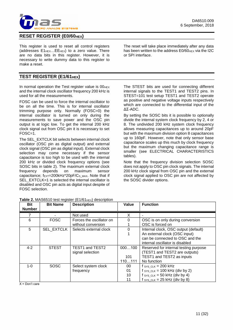
TEST REGISTER (E1/61HEX) In normal operation the Test register value is 00HEX and the internal clock oscillator frequency 200 kHz is used for all the measurements.
FOSC can be used to force the internal oscillator to be on all the time. This is for internal oscillator trimming purpose only. Normally (FOSC=0) the internal oscillator is turned on only during the measurements to save power and the OSC pin output is at logic low. To get the internal 200 kHz clock signal out from OSC pin it is necessary to set FOSC=1.
The SEL_EXTCLK bit selects between internal clock oscillator (OSC pin as digital output) and external clock signal (OSC pin as digital input). External clock selection may come necessary if the sensor capacitance is too high to be used with the internal 200 kHz or divided clock frequency options (see SOSC bits in table 2). The maximum external clock frequency depends on maximum sensor capacitance; fEXT=200kHz*20pF/CS_MAX. Note that if SEL_EXTCLK=1 is selected the internal oscillator is disabled and OSC pin acts as digital input despite of FOSC selection.
The STEST bits are used for connecting different internal signals to the TEST1 and TEST2 pins. In STEST=101 test setup TEST1 and TEST2 operate as positive and negative voltage inputs respectively which are connected to the differential input of the ΔΣ-ADC.
By setting the SOSC bits it is possible to optionally divide the internal system clock frequency by 2, 4 or 8. The undivided 200 kHz system clock frequency allows measuring capacitances up to around 20pF but with the maximum division option 8 capacitances up to 160pF. However, note that only sensor base capacitance scales up this much by clock frequency but the maximum changing capacitance range is smaller (see ELECTRICAL CHARACTERISTICS tables).
Note that the frequency division selection SOSC does not apply to OSC pin clock signals. The internal 200 kHz clock signal from OSC pin and the external clock signal applied to OSC pin are not affected by the SOSC divider options.
Table 2. MAS6510 test register (E1/61HEX) description
Bit Number
Bit Name Description Value Function
7 - Not used X -
6 FOSC Forces the oscillator on without conversion
0 1
OSC is on only during conversion OSC is forced on
5 SEL_EXTCLK Selects external clock 0 1
Internal clock, OSC output (default) An external clock (OSC input) can be connected to OSC and the internal oscillator is disabled
4-2 STEST TEST1 and TEST2 signal selection
000…100
101 110…111
Reserved for internal testing purpose (TEST1 and TEST2 are outputs) TEST1 and TEST2 as inputs No function
1-0 SOSC Select system clock frequency
00 01 10 11
f SYS_CLK = 200 kHz f SYS_CLK = 100 kHz (div by 2) f SYS_CLK = 50 kHz (div by 4) f SYS_CLK = 25 kHz (div by 8)
X = Don’t care
DA6510.009
6 September, 2018
12 (32)
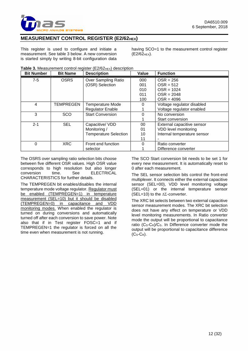
MEASUREMENT CONTROL REGISTER (E2/62HEX) This register is used to configure and initiate a measurement. See table 3 below. A new conversion is started simply by writing 8-bit configuration data
having SCO=1 to the measurement control register (E2/62HEX).
Table 3. Measurement control register (E2/62HEX) description
Bit Number Bit Name Description Value Function
7-5 OSRS Over Sampling Ratio (OSR) Selection
000 001 010 011 100
OSR = 256 OSR = 512 OSR = 1024 OSR = 2048 OSR = 4096
4 TEMPREGEN Temperature Mode Regulator Enable
0 1
Voltage regulator disabled Voltage regulator enabled
3 SCO Start Conversion 0 1
No conversion Start conversion
2-1 SEL Capacitive/ VDD Monitoring / Temperature Selection
00 01 10 11
External capacitive sensor VDD level monitoring Internal temperature sensor -
0 XRC Front end function selector
0 1
Ratio converter Difference converter
The OSRS over sampling ratio selection bits choose between five different OSR values. High OSR value corresponds to high resolution but also longer conversion time. See ELECTRICAL CHARACTERISTICS for further details.
The TEMPREGEN bit enables/disables the internal temperature mode voltage regulator. Regulator must be enabled (TEMPREGEN=1) in temperature measurement (SEL=10) but it should be disabled (TEMPREGEN=0) in capacitance and VDD monitoring modes. When enabled the regulator is turned on during conversions and automatically turned off after each conversion to save power. Note also that if in Test register FOSC=1 and if TEMPREGEN=1 the regulator is forced on all the time even when measurement is not running.
The SCO Start conversion bit needs to be set 1 for every new measurement. It is automatically reset to 0 after each measurement.
The SEL sensor selection bits control the front-end multiplexer. It connects either the external capacitive sensor (SEL=00), VDD level monitoring voltage (SEL=01) or the internal temperature sensor
(SEL=10) to the -converter.
The XRC bit selects between two external capacitive sensor measurement modes. The XRC bit selection does not have any effect on temperature or VDD level monitoring measurements. In Ratio converter mode the output will be proportional to capacitance ratio (CS-CR)/CS. In Difference converter mode the output will be proportional to capacitance difference (CS-CR).
DA6510.009
6 September, 2018
13 (32)
INTERNAL CS AND CR CAPACITOR MATRIX REGISTERS (E3/63HEX AND E4/64HEX) There are two internal capacitor matrices CS_INT and CR_INT that add capacitance in parallel to external sensor capacitor (CS_EXT) and external reference capacitor (CR_EXT) respectively. See application figure 9 on page 30. These offset capacitances are used to adjust the sensor signal to an optimal CDC input range. Each capacitor matrix has a selectable capacitance from 0pF up to 22pF in typical 86.3fF steps. The three sigma process variation of the capacitor matrix capacitance is ±10%.
The CS_INT capacitor matrix is controlled by 8-bit register (E3/63HEX) value OCDACS. See table 4. It has a corresponding EEPROM address (C3/43HEX) as non-volatile storage of the trim value. The CR_INT capacitor matrix is controlled by 8-bit register
(E4/64HEX) value OCDACR. See table 5. It has also corresponding EEPROM address (C4/44HEX) as non-volatile storage of the trim value. The internal CS_INT and CR_INT capacitor matrix capacitance values depend on OCDACS and OCDACR register values according to equations 1-2.
After finding suitable CS_INT and CR_INT capacitor matrix register values the trim values can be stored in the corresponding non-volatile EEPROM addresses.
In normal operating mode these trim values are automatically read from the EEPROM during each conversion start. See also table 10 Trimming control Register (EE/6EHEX) for other operating modes.
25522_
OCDACSpFC INTS = Equation 1.
25522_
OCDACRpFC INTR = Equation 2.
Table 4. CS_INT internal capacitor matrix register (E3/63HEX), EEPROM address (C3/43HEX)
Bit Number Bit Name Description Value Function
7-0 OCDACS CDAC control bits 00HEX…FFHEX CS_INT offset trimming
Table 5. CR_INT internal capacitor matrix register (E4/64HEX), EEPROM address (C4/44HEX)
Bit Number Bit Name Description Value Function
7-0 OCDACR CDAC control bits 00HEX…FFHEX CR_INT offset trimming
GAIN REGISTER (E5/65HEX) The 8-bit gain register (E5/65HEX) value (GRDAC) adjusts excitation signal level for the capacitive sensor. See table 6. Larger register value corresponds to smaller input changing capacitance range and vice versa. The gain register together with the CS_INT and the CR_INT capacitor matrix trim parameters define input capacitance range of measurement. Ideally the sensor signal is fit perfectly within the linear input capacitance range of
the CDC. Such trimming maximizes resolution and dynamic range of the measurement.
The gain register (E5/65HEX) has a corresponding EEPROM address (C5/45HEX) as non-voltage storage of the trim value. After finding a suitable gain register value it can be stored in the non-volatile EEPROM memory. In normal operating mode the gain trim value is read automatically from the EEPROM during each conversion start.
Table 6. Gain register (E5/65HEX), EEPROM address (C5/45HEX)
Bit Number Bit Name Description Value Function
7-0 GRDAC RDAC control bits 00HEX…FFHEX Gain adjustment by sensor excitation signal level control
DA6510.009
6 September, 2018
14 (32)
OSCILLATOR FREQUENCY CONTROL REGISTER (E6/66HEX) Note that the internal clock oscillator frequency has been factory trimmed and the trim value has been stored in the EEPROM (C6/46HEX). It is recommended not to change the factory programmed value! The oscillator frequency control register (E6/66HEX) is for trimming the internal clock oscillator to 200 kHz
frequency. This 200 kHz can be measured at the OSC pin. The six LSB bits adjust the oscillator period in 104ns steps. The period increases when the trim value increases. Typically a register value of 28HEX corresponds to the nominal 200 kHz clock oscillator frequency. After finding a suitable trim value it can be stored to the EEPROM (C6/46HEX).
Table 7. Oscillator frequency control register (E6/66HEX)
Bit Number Bit Name Description Value Function
5-0 OSCF Oscillator frequency control bits
00HEX…3FHEX Oscillator frequency control
EEPROM DATA INPUT REGISTER (E8/68HEX) This register can be ignored by user. It is related to internal EEPROM operations and updated
automatically during every EEPROM write operation.
EEPROM WRITE ENABLE REGISTER (E9/69HEX) The EEPROM is normally write protected. To enable write the EEPROM write enable register should be set to %00000100 (04HEX). To disable write the register should be set to %00000000 (00HEX) which is the register default value after power-on-rest or
manual reset by XCLR or reset register. Note: don’t use any other EEPROM write enable register values than these two since other register bits are reserved for internal testing purpose only.
Table 8. EEPROM write enable register (E9/69HEX)
Bit Number Bit Name Description Value Function
7-3 00000 Reserved. Keep these bits always 0.
2 EWE EEPROM write enable 0 1
EEPROM write disabled EEPROM write enabled
1-0 00 Reserved. Keep these bits always 0.
After a power-on-reset and in normal operation the EEPROM write enable register has the default value 00HEX.
DA6510.009
6 September, 2018
15 (32)
CONVERSION RESULT REGISTERS (EA…ECHEX) After measuring capacitance, temperature or supply voltage the 24-bit conversion result is stored into three register addresses EA…ECHEX. The MSB
(most significant byte) is at EAHEX, ISB (intermediate significant byte) at EBHEX and LSB (least significant byte) at ECHEX.
EEPROM STATUS REGISTER (ED/6DHEX) The EEPROM status register (ED/6DHEX) indicates if the stored EEPROM byte is corrupted. The register is updated after each EEPROM data byte read command. See table 9 below. The ERROR bit tells whether a data error has been detected or not. The
DED bit tells whether two or more bit errors have been detected. The EEPROM can correct internally only single bit errors i.e. when ERROR=1 and DED=0. The read EEPROM data byte is corrupted if ERROR=DED=1.
Table 9. MAS6510 EEPROM status register (ED/6DHEX). Only bits (7:6) are used.
Bit Number Bit Name Description Value Function
7 ERROR EEPROM error detection 0 1
No errors Error detected
6 DED EEPROM double error detection 0 1
No errors 2 (or more) data errors
5-0 000000 -
TRIMMING CONTROL REGISTER (EE/6EHEX) The Trimming control register (EE/6EHEX) is used to select between different trimming operating modes. See table 10 showing the functions of the Trimming control register.
After a power-up reset, master reset via XCLR or a software reset via serial bus the Trimming control register (EE/6EHEX) gets the value %00000000 (00HEX). This is the normal operating mode for a trimmed MAS6510 device. In this mode the capacitive front-end trim values to use (CS, CR and Gain) are automatically read from the EEPROM memory in the beginning of each conversion start.
When calibrating a sensor there is an operating mode in which only the factory calibrated internal
oscillator (OSC) clock trim data is read from the EEPROM memory. This mode is selected by writing %10101010 (AAHEX) to the Trimming control register. In this mode it is possible to run conversion tests for different front-end trim register values before suitable values are found and programmed to the EEPROM.
There is also a trimming mode in which all trim data including the internal oscillator trim data is taken from the trim registers rather than from the EEPROM. This mode is selected by writing %11111111 (FFHEX) to the Trimming control register.
Table 10. Trimming control Register (EE/6EHEX)
Bit Number Bit Name Description Value Function
7-0 REGEE<7:0> EEPROM control bits 00000000 10101010 11111111 OTHER
All trim data from EEPROM (normal operating mode) Only OSC from EEPROM All trim data from registers All trim data from EEPROM
DA6510.009
6 September, 2018
16 (32)
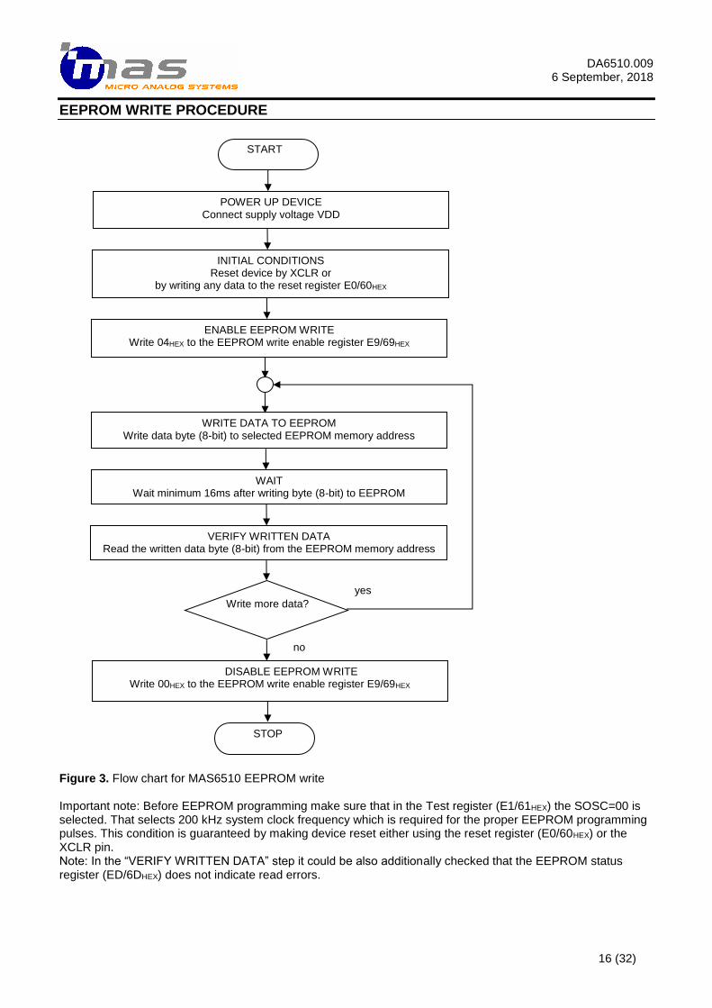
EEPROM WRITE PROCEDURE
Figure 3. Flow chart for MAS6510 EEPROM write Important note: Before EEPROM programming make sure that in the Test register (E1/61HEX) the SOSC=00 is selected. That selects 200 kHz system clock frequency which is required for the proper EEPROM programming pulses. This condition is guaranteed by making device reset either using the reset register (E0/60HEX) or the XCLR pin. Note: In the “VERIFY WRITTEN DATA” step it could be also additionally checked that the EEPROM status register (ED/6DHEX) does not indicate read errors.
START
INITIAL CONDITIONS Reset device by XCLR or
by writing any data to the reset register E0/60HEX
POWER UP DEVICE Connect supply voltage VDD
ENABLE EEPROM WRITE Write 04HEX to the EEPROM write enable register E9/69HEX
WAIT Wait minimum 16ms after writing byte (8-bit) to EEPROM
STOP
DISABLE EEPROM WRITE Write 00HEX to the EEPROM write enable register E9/69HEX
WRITE DATA TO EEPROM Write data byte (8-bit) to selected EEPROM memory address
no
Write more data?
yes
VERIFY WRITTEN DATA Read the written data byte (8-bit) from the EEPROM memory address
DA6510.009
6 September, 2018
17 (32)
EEPROM WRITE PROCEDURE This chapter gives instructions for writing data to the EEPROM memory.
The MAS6510 24-bit Capacitance-to-Digital Converter (CDC) has a 256 bit (32 byte) EEPROM memory. 8 bits (1 byte) has been reserved for storing internal clock oscillator trimming data and other 8 bits (1 byte) for the programmable I2C device address. There are also 24 bits (3 bytes) for trimming the capacitive sensor front-end. The remaining 216 bits (27 bytes) are free for storing sensor calibration data and other use.
See figure 3 on previous page showing the EEPROM write procedure.
Make sure in the beginning of the EEPROM write procedure that the MAS6510 initial conditions are met. Connecting VDD triggers power-on-reset (POR) but to make sure the device is reset an additional reset should be given using the XCLR pin or writing any data on the reset register E0/60HEX via the serial bus. The device reset will guarantee that SOSC=00 is selected in the test register (E1/61HEX).
This selects 200 kHz clock which is required in the EEPROM programming.
EEPROM write is enabled by writing value 04HEX to the EEPROM write enable register (E9/69HEX). The default register value after power on is 00HEX.
Next the data can be written to the EEPROM memory one byte (8-bit) at a time. It is necessary to have a delay of minimum 16ms after programming each byte (8-bit). The success of each write can be verified by reading back the data (8-bit) and comparing it to the original byte (8-bit). Additionally, it is also possible to check the EEPROM status register (ED/6DHEX) value after each read back. The EEPROM status register value should be 00HEX when the read EEPROM data byte is free of errors.
After all data bytes are written the EEPROM memory can be protected from write by writing 00HEX to the EEPROM write enable register (E9/69HEX).
See table 1 showing the MAS6510 register and EEPROM data addresses.
DA6510.009
6 September, 2018
18 (32)
SERIAL DATA INTERFACE CONTROL Serial Interface MAS6510 can be operated either via 2-wire serial I2C bus or via 4-wire serial SPI bus. Selection between I2C and SPI communication is done by XSPI pin. XSPI=high selects I2C and XSPI=low selects SPI communication.
2-wire serial I2C bus type interface comprises of serial clock input (SCL) and bi-directional serial data (SDA) input/output. I2C bus is used to write configuration data to sensor interface IC and read the measurement result when A/D conversion has been finished. The interface is also used for reading the calibration EEPROM memory.
Note: The 2-wire I2C bus of MAS6510 supports only basic I2C bus communication protocol but not for example 10-bit addressing, arbitration and clock stretching features of the I2C bus specification.
The alternative 4-wire serial SPI bus type interface comprises of serial clock input (SCLK), serial data
input (MOSI), serial data output (MISO) and chip select input (XCS).
Digital interface includes also end of conversion (EOC) and master reset (XCLR) pins. Rising edge in the EOC pin indicates that the conversion is ready and the result can be read out through serial interface.
XCLR is used to reset the MAS6510. A reset initializes registers (set to value 00HEX), counters and the serial communication bus. Alternatively, device can be reset via serial bus by writing any data to Reset register (address E0/60HEX). The Reset register bits don’t have any function. Reading from the reset register is not possible.
After connecting the supply voltage to MAS6510, and before starting operating the device via the serial bus it is recommended to reset the device manually after every power up to guarantee proper register settings after any VDD rise conditions
I2C Bus Communication In MAS6510 the I2C bus communication is selected by setting XSPI pin high.
The I2C bus standard makes it possible to connect several devices on same bus. The devices are distinguished from each other by unique device addresses. In MAS6510 there is both a hard wired and programmable device address. Both hard wired and programmable addresses can be used to address MAS6510. The MAS6510 hard wired device address is shown in the following table. The LSB bit of the device address defines whether the bus is configured to Read (1) or Write (0) operation.
The programmable device address is located in the EEPROM register C2HEX which has been factory programmed to value ECHEX (%11101100) which is the same as the fixed device address of MAS6510. When unique device address is needed it can be programmed to this register. The programmable I2C device address is read from EEPROM memory only during power on reset or manual reset situations. To guarantee that the programmable address is read from EEPROM the device can be reset manually by using XCLR pin or Reset register (E0/60HEX).
Table 11. MAS6510 hard wired I2C bus device address (EC/EDHEX)
A7 A6 A5 A4 A3 A2 A1 W/R
1 1 1 0 1 1 0 0/1
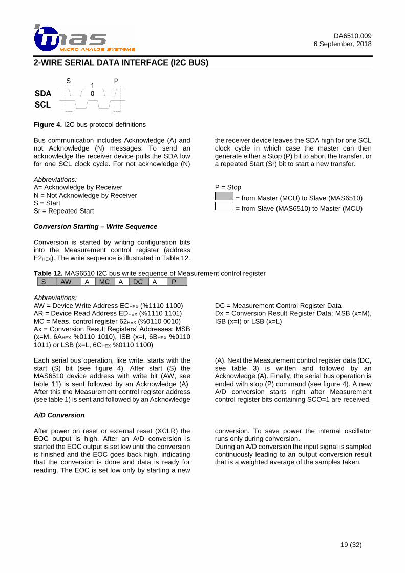
I2C Bus Protocol Definitions Data transfer is initiated with a Start bit (S) when SDA is pulled low while SCL stays high. Then, SDA sets the transferred bit while SCL is low and the data is sampled (received) when SCL rises. When the transfer is complete, a Stop bit (P) is sent by releasing the data line to allow it to be pulled up while SCL is constantly high.
Figure 4 shows the start (S) and stop (P) bits and a data bit. Data must be held stable at the SDA pin
when SCL is high. Data at the SDA pin can change value only when SCL is low.
Each SDA line byte transfer must contain 8-bits where the most significant bit (MSB) always comes first. Each byte has to be followed by an acknowledge bit (see further below). The number of bytes transmitted per transfer is unrestricted.
DA6510.009
6 September, 2018
19 (32)
2-WIRE SERIAL DATA INTERFACE (I2C BUS)
Figure 4. I2C bus protocol definitions Bus communication includes Acknowledge (A) and not Acknowledge (N) messages. To send an acknowledge the receiver device pulls the SDA low for one SCL clock cycle. For not acknowledge (N)
the receiver device leaves the SDA high for one SCL clock cycle in which case the master can then generate either a Stop (P) bit to abort the transfer, or a repeated Start (Sr) bit to start a new transfer.
Abbreviations: A= Acknowledge by Receiver N = Not Acknowledge by Receiver S = Start Sr = Repeated Start
P = Stop
= from Master (MCU) to Slave (MAS6510)
= from Slave (MAS6510) to Master (MCU)
Conversion Starting – Write Sequence Conversion is started by writing configuration bits into the Measurement control register (address E2HEX). The write sequence is illustrated in Table 12. Table 12. MAS6510 I2C bus write sequence of Measurement control register
S AW A MC A DC A P
Abbreviations: AW = Device Write Address ECHEX (%1110 1100) AR = Device Read Address EDHEX (%1110 1101) MC = Meas. control register 62HEX (%0110 0010) Ax = Conversion Result Registers’ Addresses; MSB (x=M, 6AHEX %0110 1010), ISB (x=I, 6BHEX %0110 1011) or LSB (x=L, 6CHEX %0110 1100)
DC = Measurement Control Register Data Dx = Conversion Result Register Data; MSB (x=M), ISB (x=I) or LSB (x=L)
Each serial bus operation, like write, starts with the start (S) bit (see figure 4). After start (S) the MAS6510 device address with write bit (AW, see table 11) is sent followed by an Acknowledge (A). After this the Measurement control register address (see table 1) is sent and followed by an Acknowledge
(A). Next the Measurement control register data (DC, see table 3) is written and followed by an Acknowledge (A). Finally, the serial bus operation is ended with stop (P) command (see figure 4). A new A/D conversion starts right after Measurement control register bits containing SCO=1 are received.
A/D Conversion After power on reset or external reset (XCLR) the EOC output is high. After an A/D conversion is started the EOC output is set low until the conversion is finished and the EOC goes back high, indicating that the conversion is done and data is ready for reading. The EOC is set low only by starting a new
conversion. To save power the internal oscillator runs only during conversion. During an A/D conversion the input signal is sampled continuously leading to an output conversion result that is a weighted average of the samples taken.
DA6510.009
6 September, 2018
20 (32)
2-WIRE SERIAL DATA INTERFACE (I2C BUS) Conversion Result – Read Sequence Table 13 presents a general control sequence for a single register data read. Table 13. MAS6510 I2C bus single register (address Ax) read sequence bits
S AW A Ax A Sr AR A Dx N P
Table 14 shows the control sequence for reading the 24-bit A/D conversion result from the Conversion result registers. The ISB (DI) and LSB (DL) register data read can follow right after the MSB register data
(DM) read since if the read sequence is continued (not ended by a Stop bit P) the register address is automatically incremented to point to the next register.
Table 14. MAS6510 I2C bus MSB (first), MID (second) and LSB (third) A/D conversion result read sequence
S AW A AM A Sr AR A DM A DI A DL N P
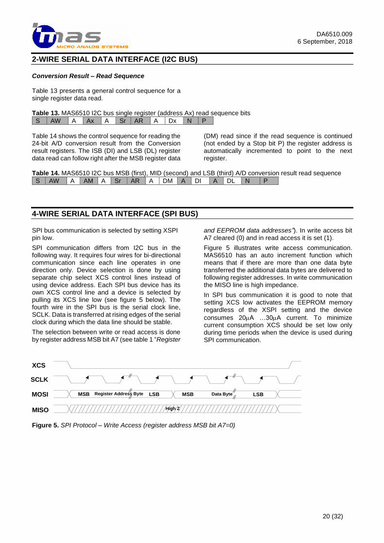
4-WIRE SERIAL DATA INTERFACE (SPI BUS) SPI bus communication is selected by setting XSPI pin low.
SPI communication differs from I2C bus in the following way. It requires four wires for bi-directional communication since each line operates in one direction only. Device selection is done by using separate chip select XCS control lines instead of using device address. Each SPI bus device has its own XCS control line and a device is selected by pulling its XCS line low (see figure 5 below). The fourth wire in the SPI bus is the serial clock line, SCLK. Data is transferred at rising edges of the serial clock during which the data line should be stable.
The selection between write or read access is done by register address MSB bit A7 (see table 1 “Register
and EEPROM data addresses”). In write access bit A7 cleared (0) and in read access it is set (1).
Figure 5 illustrates write access communication. MAS6510 has an auto increment function which means that if there are more than one data byte transferred the additional data bytes are delivered to following register addresses. In write communication the MISO line is high impedance.
In SPI bus communication it is good to note that setting XCS low activates the EEPROM memory regardless of the XSPI setting and the device
consumes 20A …30A current. To minimize current consumption XCS should be set low only during time periods when the device is used during SPI communication.
XCS
SCK
SDA
MISO
MSB LSBRegister Address Byte MSB LSBData Byte
High Z
Figure 5. SPI Protocol – Write Access (register address MSB bit A7=0)
SCLK
MOSI
DA6510.009
6 September, 2018
21 (32)
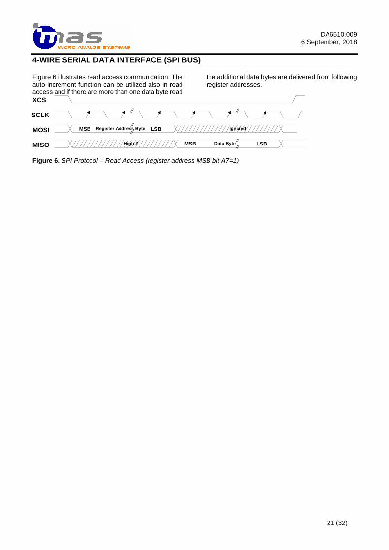
4-WIRE SERIAL DATA INTERFACE (SPI BUS) Figure 6 illustrates read access communication. The auto increment function can be utilized also in read access and if there are more than one data byte read
the additional data bytes are delivered from following register addresses.
XCS
SCK
SDA
MISO
MSB LSBRegister Address Byte
High Z MSB LSBData Byte
Ignored
Figure 6. SPI Protocol – Read Access (register address MSB bit A7=1)
SCLK
MOSI
DA6510.009
6 September, 2018
22 (32)
CAPACITANCE MEASUREMENT MODES MAS6510 has two capacitance measurement modes. Selection between modes is done by XRC bit in the Measurement control register (E2/62HEX). Capacitance difference mode is selected by XRC=1 and capacitance ratio mode by XRC=0. See table 3 on page 12.
Capacitance difference mode
In the capacitance difference mode the CDC output result (CODE) is proportional to capacitance difference
C=(CS-CR) where the CS is overall capacitance between CS and CC pins and the CR is overall capacitance between CR and CC pins. See equation 3.
−+=
+= DIFF
REF
RS
DIFF
REF
KC
CCCODEFSK
C
CCODEFSCODE 1
21
2 Equation 3.
where
CODEFS = Maximum output code range which depends on OSR selection. See page 7 “Full scale output code range” specification in the ELECTRICAL CHARACTERISTICS table.
KDIFF = 0.229+0.02*GRDAC (see table 6 for Gain register setting) Equation 4. CREF = 6pF ±10% Internal reference capacitor CS = CS_EXT + CS_INT External sensor + internal sensor matrix capacitance Equation 5a.
between CS and CC pins CR = CR_EXT + CR_INT External reference + internal reference matrix capacitance Equation 5b.
between CR and CC pins
CEXT = CS_EXT – CR_EXT Capacitance difference of external capacitances
CINT = CS_INT – CR_INT Capacitance difference of internal offset capacitance matrices Equation 5c.
C = (CS-CR) = (CS_EXT + CS_INT) - (CR_EXT + CR_INT) = CEXT + CINT Equation 5d. Overall capacitance difference
In capacitance difference mode either CS_EXT, CR_EXT or both external capacitances can vary. Substituting equation 5d to equation 3 lead to equation 6.
++= DIFF
REF
INTEXT KC
CCCODEFSCODE 1
2 Equation 6.
From equations 5c and 6 we see that offset trimming of the CODE is achieved using internal capacitance matrices
which define the CINT = CS_INT – CR_INT term. Increasing CS_INT increases CODE and increasing CR_INT decreases CODE. The CS_INT and CR_INT capacitances are adjusted by OCDACS and OCDACR settings respectively (see Internal capacitor matrix registers in tables 4 and 5). Gain trimming is achieved by gain register GRDAC value (see Gain register in table 6) which adjusts gain coefficient (KDIFF) according to equation 4.
The CDC output result (CODE) ranges from 0 to CODEFS. These correspond to following minimum (CEXT_MIN)
and maximum (CEXT_MAX) external input capacitance difference and overall external changing capacitance
(CEXT_TOT) values.
INT
DIFF
REFMINEXT C
K
CC −−= _ , INT
DIFF
REFMAXEXT C
K
CC −= _ Equations 7a, 7b
DIFF
REFMINEXTMAXEXTTOTEXT
K
CCCC =−= 2___ Equations 7c.
However linear measurement range of CDC is from 10% to 90% of CODEFS. To avoid non-linearity error in the measurements the capacitive front-end should be trimmed to keep the measured external capacitance within the
linear measurement range of the CDC. In the linear measurement range the minimum (CEXT_LIN_MIN) and
maximum (CEXT_LIN_MAX) external capacitance difference and overall external changing capacitance
(CEXT_LIN_TOT) values are as follows.
DA6510.009
6 September, 2018
23 (32)
CAPACITANCE MEASUREMENT MODES (continued)
INT
DIFF
REFMINLINEXT C
K
CC −−= %80__ , INT
DIFF
REFMAXLINEXT C
K
CC −= %80__ Equations 8a, 8b.
TOTEXT
DIFF
REFMINLINEXTMAXLINEXTTOTLINEXT C
K
CCCC _______ 8.06.1 ==−= Equation 8c.
Example:
GRDAC = 109DEC, OCDACS = 0DEC and OCDACR = 93DEC trim settings correspond to following external input capacitance difference measurement range values.
Capacitance values of offset capacitance matrices:
CS_INT = 22pF*0/255 = 0pF, CR_INT = 22pF*93/255 8.03pF, CINT = 0pF - 8.03pF = -8.03pF
Gain coefficient: KDIFF = 0.229+0.02*109 = 2.409
Overall input range:
CEXT_MIN = -6pF/2.409-(-8.03pF) 5.54pF
CEXT_MAX = 6pF/2.409-(-8.03pF) 10.52pF
CEXT_TOT = 2*6pF/2.409 4.98pF
Linear input range:
CEXT_LIN_MIN = -0.8*6pF/2.409-(-8.03pF) 6.04pF
CEXT_LIN_MAX = 0.8*6pF/2.409-(-8.03pF) 10.02pF
CEXT_LIN_TOT = 0.8*4.98pF 3.98pF
Note that above calculated values are capacitance difference values between external sensor (CS) and external
reference (CR) side capacitances (CEXT = CS_EXT – CR_EXT). If there is no external reference capacitor (CR_EXT=0)
then these values represent sensor side (CS) capacitance CS_EXT (CEXT = CS_EXT – 0= CS_EXT) minimum and maximum measurement range values. If a fixed external reference capacitor CR_EXT exists then sensor side (CS)
capacitance measurement range is CR_EXT added to above CEXT values (CS_EXT = CEXT + CR_EXT). If CR_EXT is
also varying then above values tell range of CS_EXT and CR_EXT capacitance difference (CEXT = CS_EXT – CR_EXT) that can be measured.
Capacitance ratio mode
In the capacitance ratio mode the CDC output result (CODE) is proportional to capacitance ratio (CS-CR)/CS.
RATIO
INTSEXTS
INTREXTR
RATIO
S
R KCC
CCCODEFSK
C
CCODEFSCODE
+
+−=
−=
__
__11 Equation 9.
where
CODEFS = Maximum output code range which depends on OSR selection. See page 7 “Full scale output code range” specification in the ELECTRICAL CHARACTERISTICS table.
KRATIO = 193.8/GRDAC (see table 6 for Gain register setting) Equation 10. CS = CS_EXT + CS_INT External sensor + internal sensor matrix capacitance between CS and CC pins CR = CR_EXT + CR_INT External reference + internal reference matrix capacitance between CR and CC pins
DA6510.009
6 September, 2018
24 (32)
TRIMMING FOR SENSOR CAPACITANCE
MAS6510 in capacitance difference mode Optimal trim settings which adjust capacitive signal to linear conversion range 10%...90% of the CDC are calculated as follows. At first offset COFS_EXT of external capacitance ranges CS_EXT and CR_EXT is calculated.
COFS_EXT = (CEXT_MIN + CEXT_MAX) / 2 =
= (CS_EXT_MIN – CR_EXT_MAX + CS_EXT_MAX – CR_EXT_MIN) / 2 Equation 11.
The offset compensated to zero by using either CS_INT or CR_INT capacitor matrices depending on the offset polarity.
If COFS_EXT ≥ 0pF
then CR_INT = COFS_EXT and CS_INT = 0pF
else CR_INT = 0pF and CS_INT = -COFS_EXT
Corresponding capacitance matrix register values (decimal) are calculated as follows.
REGE3HEX = OCDACS = (CS_INT/22pF)*255DEC Equation 12.
REGE4HEX = OCDACR = (CR_INT/22pF)*255DEC Equation 13.
Optimal gain coefficient (KDIFF) value scales capacitive signal to linear conversion range 10%...90% of the CDC and it is calculated as follows.
KDIFF = 1.6*CREF / (CEXT_MAX - CEXT_MIN) =
= 1.6*CREF / (CS_EXT_MAX – CS_EXT_MIN + CR_EXT_MAX - CR_EXT_MIN) Equation 14.
where CREF = 6pF ±10%.
Corresponding Gain register (REGE5HEX) value (decimal) can be solved from the equation 4 presented on page 22 as follows.
REGE5HEX = GRDAC = (KDIFF-0.229)/0.02 Equation 15.
Example 1: No external reference capacitor CR_EXT CS_EXT_MIN = 8pF and CR_EXT_MAX = 0pF at sensed parameter (pressure, humidity etc.) minimum
CS_EXT_MAX = 12pF and CR_EXT_MIN = 0pF at sensed parameter (pressure, humidity etc.) maximum CR_OFS_EXT = (8pF-0pF+12pF-0pF)/2=10pF
COFS_EXT ≥ 0 CR_INT = COFS_EXT = 10pF and CS_INT = 0 pF
KDIFF = 1.6*6pF/(12pF-8pF+0pF-0pF) = 2.4 REGE3HEX = OCDACS = (0pF/22pF)*255 = 0DEC (CS capacitor matrix)
REGE4HEX = OCDACR = (10pF/22pF)*255 = 115.91 116DEC (CR capacitor matrix)
REGE5HEX = GRDAC = (2.4-0.229)/0.02 = 108.55 109DEC (Gain register)
Example 2: Both CS_EXT and CR_EXT vary but to opposite directions CS_EXT_MIN = 10pF and CR_EXT_MAX = 14.5pF at sensed parameter (pressure, humidity etc.) minimum
CS_EXT_MAX = 14pF and CR_EXT_MIN = 10pF at sensed parameter (pressure, humidity etc.) maximum COFS_EXT = (10pF-14.5pF+14pF-10pF)/2 = -0.25pF
COFS_EXT < 0 CR_INT = 0pF and CS_INT = -COFS_EXT = 0.25pF
KDIFF = 1.6*6pF/(14pF-10pF+14.5pF-10pF) = 1.129
REGE3HEX = OCDACS = (0.25pF/22pF)*255 = 2.90 3DEC (CS capacitor matrix) REGE4HEX = OCDACR = (0pF/22pF)*255 = 0DEC (CR capacitor matrix)
REGE5HEX = GRDAC = (1.129-0.229)/0.02 = 45.00 45DEC (Gain register)
The found REGE3HEX, REGE4HEX and REGE5HEX trim register values need to be stored to corresponding non-volatile EEPROM addresses. In I2C communication these are C3HEX, C4HEX and C5HEX but in SPI write communication the addresses are 43HEX, 44HEX and 45HEX since in SPI write the MSB address bit is 0. See table 1 on page 9.
DA6510.009
6 September, 2018
25 (32)
TRIMMING FOR SENSOR CAPACITANCE (continued)
MAS6510 in capacitance ratio mode Optimal trim settings which adjust capacitive signal to linear conversion range 10%...90% of the CDC are found as follows.
COFS = [0.9*CS_EXT_MAX*(CS_EXT_MIN – CR_EXT_MAX) – 0.1*CS_EXT_MIN *(CS_EXT_MAX - CR_EXT_MIN)] / [0.9*CS_EXT_MAX - 0.1*CS_EXT_MIN] Equation 16.
If COFS ≥ 0pF
then CR_INT = COFS and CS_INT = 0pF
else CR_INT = 0pF and CS_INT is calculated as follows.
a = 0.8 b = 0.9*(CS_EXT_MAX + CS_EXT_MIN – CR_EXT_MAX) – 0.1*(CS_EXT_MAX + CS_EXT_MIN - CR_EXT_MIN) Equation 17a. c = 0.9*CS_EXT_MAX *(CS_EXT_MIN – CR_EXT_MAX) – 0.1*CS_EXT_MIN *(CS_EXT_MAX - CR_EXT_MIN) Equation 17b.
CS_INT1 = [-b+(b^2-4*a*c)]/2/a Equation 17c.
CS_INT2 = [-b-(b^2-4*a*c)]/2/a Equation 17d.
If CS_INT1 ≥ 0pF then CS_INT = CS_INT1 else CS_INT= CS_INT2
If CR_EXT does not exist (CR_EXT = 0pF) the equation 16 simplifies to following form.
COFS = CR_INT = 0.8*CS_EXT_MAX*CS_EXT_MIN / (0.9*CS_EXT_MAX - 0.1*CS_EXT_MIN) Equation 18.
Corresponding capacitance matrix register (REGE3HEX and REGE4HEX) values (decimal) are calculated using equations 12 and 13 presented on page 24.
Optimal gain coefficient (KRATIO) value is calculated as follows.
KRATIO = 0.1 * (CS_EXT_MIN + CS_INT) / (CS_EXT_MIN + CS_INT – CR_EXT_MAX - CR_INT) = Equation 19a. = 0.9 * (CS_EXT_MAX + CS_INT) / (CS_EXT_MAX + CS_INT – CR_EXT_MIN - CR_INT) Equation 19b.
Corresponding Gain register (REGE5HEX) value (decimal) can be solved from the equation 10 presented on page 23 as follows.
GRDAC = 193.8/ KRATIO (see table 6 for Gain register setting) Equation 20.
Example 1: Only CS_EXT varies and CR_EXT does not exist (CR_EXT = 0pF)
CS_EXT_MIN=4pF at sensed parameter (pressure, humidity etc.) minimum CS_EXT_MAX=12pF at sensed parameter (pressure, humidity etc.) maximum
CR_EXT_MIN/MAX = 0pF (no external reference capacitor)
COFS = 0.8*12pF*4pF/(0.9*12pF-0.1*4pF) = 3.69pF ≥ 0 CR_INT = COFS = 3.69pF and CS_INT = 0pF KRATIO = 0.1*(4pF+0pF)/(4pF-0pF-0pF-3.69pF) = 1.3
REGE3HEX = OCDACS = (0pF/22pF)*255 = 0DEC (CS capacitor matrix)
REGE4HEX = OCDACR = (3.69pF/22pF)*255 43DEC (CR capacitor matrix)
REGE5HEX = GRDAC = 193.8/1.3 = 149.08 149DEC (Gain register)
DA6510.009
6 September, 2018
26 (32)
TRIMMING FOR SENSOR CAPACITANCE (continued) Example 2: Only CS_EXT varies but fixed CR_EXT exists
CS_EXT_MIN=9pF and CR_EXT_MAX=10pF at sensed parameter (pressure, humidity etc.) minimum
CS_EXT_MAX=14pF and CR_EXT_MIN=10pF at sensed parameter (pressure, humidity etc.) maximum
COFS = [0.9*14pF*(9pF-10pF)-0.1*9pF*(14pF-10pF)]/(0.9*14pF-0.1*9pF)= -1.38pF < 0 CR_INT = 0pF a = 0.8 b = 0.9*(14pF+9pF-10pF)-0.1*(14pF+9pF-10pF)= 10.4pF c = 0.9*14pF*(9pF-10pF)-0.1*9pF*(14pF-10pF)= -16.2 pF^2
CS_INT1 = {-10.4pF+ [(10.4pF)^2-4*0.8*(-16.2)pF^2]}/2/0.8= 1.406pF
CS_INT2 = {-10.4pF- [(10.4pF)^2-4*0.8*(-16.2)pF^2]}/2/0.8= -14.406pF CS_INT = 1.406pF KRATIO = 0.1*(9pF+1.406pF)/(9pF+1.406pF-10pF-0pF) = 2.563
REGE3HEX = OCDACS = (1.406pF/22pF)*255 = 16.29 16DEC (CS capacitor matrix) REGE4HEX = OCDACR = (0pF/22pF)*255 = 0DEC (CR capacitor matrix)
REGE5HEX = GRDAC = 193.8/2.563 = 75.61 76DEC (Gain register)
Example 3: Both CS_EXT and CR_EXT vary but to opposite directions
CS_EXT_MIN=10pF and CR_EXT_MAX=14.5pF at sensed parameter (pressure, humidity etc.) minimum
CS_EXT_MAX=14pF and CR_EXT_MIN=10pF at sensed parameter (pressure, humidity etc.) maximum
COFS = [0.9*14pF*(10pF-14.5pF)-0.1*10pF*(14pF-10pF)]/(0.9*14pF-0.1*10pF) = -5.23pF < 0 CR_INT = 0pF a = 0.8 b = 0.9*(14pF+10pF-14.5pF)-0.1*(14pF+10pF-10pF) = 7.15pF c = 0.9*14pF*(10pF-14.5pF)-0.1*10pF*(14pF-10pF) = -60.7 pF^2
CS_INT1 = {-7.15pF+ [(7.15pF)^2-4*0.8*(-60.7)pF^2]}/2/0.8 = 5.321pF
CS_INT2 = {-7.15pF- [(7.15pF)^2-4*0.8*(-60.7)pF^2]}/2/0.8 = -14.259pF CS_INT = 5.321pF KRATIO = 0.1*(10pF+5.321pF)/(10pF+5.321pF-14.5pF-0pF) = 1.866
REGE3HEX = OCDACS = (5.321pF/22pF)*255 = 61.68 62DEC (CS capacitor matrix) REGE4HEX = OCDACR = (0pF/22pF)*255 = 0DEC (CR capacitor matrix)
REGE5HEX = GRDAC = 193.8/1.866 = 103.86 104DEC (Gain register)
The found REGE3HEX, REGE4HEX and REGE5HEX trim register values need to be stored to corresponding non-volatile EEPROM addresses. In I2C communication these are C3HEX, C4HEX and C5HEX but in SPI write communication the addresses are 43HEX, 44HEX and 45HEX since in SPI write the MSB address bit is 0. See table 1 on page 9.
DA6510.009
6 September, 2018
27 (32)
TEMPERATURE MODE The MAS6510 has an internal temperature sensor for temperature measurement. The temperature sensor output is proportional to absolute temperature (PTAT). The temperature information is needed for temperature indication and temperature compensation.
The temperature measurement is started by writing configuration data to the measurement control register (E2/62HEX). In the temperature measurement the internal regulator has to be enabled (TEMPREGEN=1) and the internal temperature sensor selected (SEL=10). The ratio and difference converter bit (XRC) selection does not have any influence on the result. Typically already the smallest
over sampling ratio (OSR) selection 256 offers sufficient resolution for the temperature measurement.
The internal temperature sensor has offset and gain variation but small non-linearity (see Electrical Characteristics table). Depending on temperature measurement accuracy requirement the offset, the gain and the non-linearity all can be compensated by external calculations. In low precision the offset and gain calibration is sufficient but in high precision the second order non-linearity calibration can be included.
Linear temperature sensor model The linear temperature measurement model for output code is following.
( )( )REFTTbaCODEFSCODE −+= Equation 21.
The OSR selects full scale output code range value CODEFS. See ELECTRICAL CHARACTERISTICS for CODEFSDIFF at different OSR values. If the temperature T is presented in °C and referenced to TREF=0°C then the typical linearized temperature sensor model parameter values a and b are as follows. a=0.38944 b=4.4329e-3 However it should be noted that the sensor has significant offset (parameter a) variation and also the gain (parameter b) has some variation and that the above values represent only typical values. The non-linearity temperature error after offset and gain calibration (best fit line) is typically <±0.5°C in the temperature range -40°C…+85°C.
2nd order temperature sensor model For higher precision the 2nd order temperature measurement model for output code is following
( ) ( )( )2
REFREF TTcTTbaCODEFSCODE −+−+= Equation 22.
If the temperature T is presented in °C and referenced to TREF=0°C then the typical 2nd order temperature sensor model parameter values a, b and c are as follows. a=0.38826 b=4.3967e-3 c=8.1098e-7 Above sensor model parameters are typical values which are subject to variations. The temperature error after offset, gain and 2nd order non-linearity calibration is typically <±0.1°C in the temperature range -40°C…+85°C.
DA6510.009
6 September, 2018
28 (32)
VDD LEVEL MONITORING MODE The MAS6510 has VDD level monitoring feature to measure supply voltage level which is useful especially in battery operated systems. In systems in which VDD can vary the VDD level monitoring could be also used to compensate VDD dependency.
The VDD level monitoring measurement is started by writing configuration data to the measurement control register (E2/62HEX). In the VDD level
monitoring mode the regulator has to be disabled (TEMPREGEN=0) and VDD level monitoring selected (SEL=01). The ratio and difference converter bit (XRC) selection does not have any influence on the result.
Typically the smallest over sampling ratio (OSR) selection 256 offers sufficient resolution for the VDD level monitoring.
VDD level monitoring model The VDD level monitoring model for output code is following.
−=
VDD
baCODEFSCODE Equation 23.
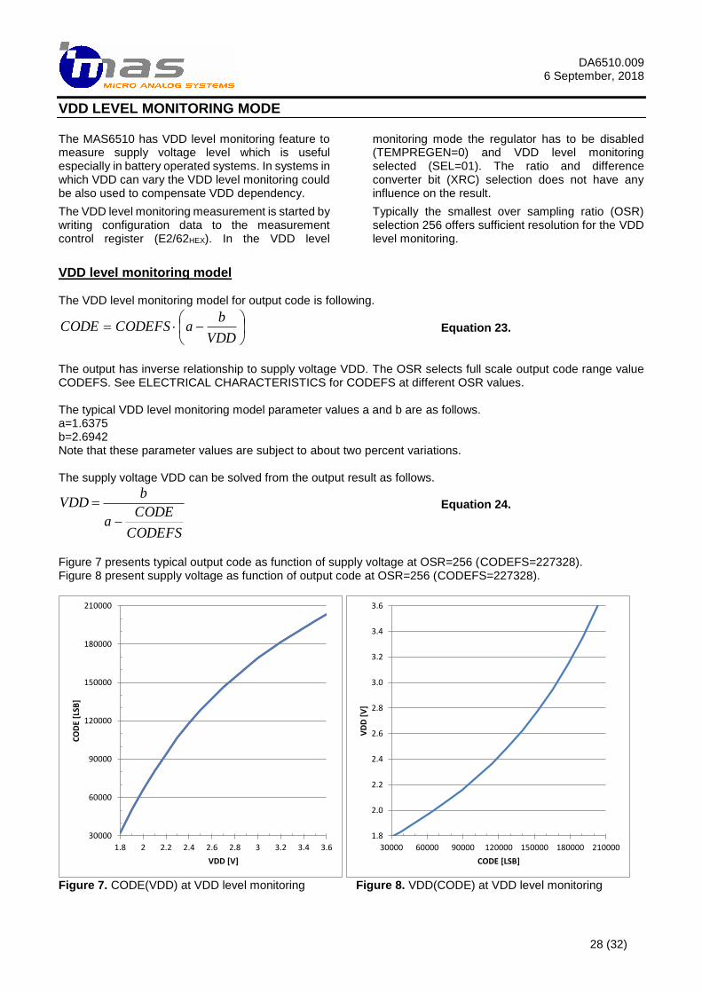
The output has inverse relationship to supply voltage VDD. The OSR selects full scale output code range value CODEFS. See ELECTRICAL CHARACTERISTICS for CODEFS at different OSR values. The typical VDD level monitoring model parameter values a and b are as follows. a=1.6375 b=2.6942 Note that these parameter values are subject to about two percent variations. The supply voltage VDD can be solved from the output result as follows.
CODEFS
CODEa
bVDD
−
= Equation 24.
Figure 7 presents typical output code as function of supply voltage at OSR=256 (CODEFS=227328). Figure 8 present supply voltage as function of output code at OSR=256 (CODEFS=227328).
Figure 7. CODE(VDD) at VDD level monitoring Figure 8. VDD(CODE) at VDD level monitoring
30000
60000
90000
120000
150000
180000
210000
1.8 2 2.2 2.4 2.6 2.8 3 3.2 3.4 3.6
CO
DE
[LSB
]
VDD [V]
1.8
2.0
2.2
2.4
2.6
2.8
3.0
3.2
3.4
3.6
30000 60000 90000 120000 150000 180000 210000
VD
D [
V]
CODE [LSB]
DA6510.009
6 September, 2018
29 (32)
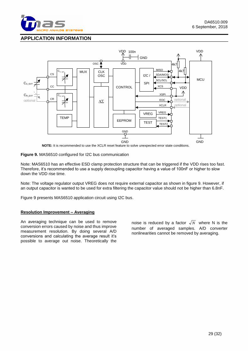
APPLICATION INFORMATION
Figure 9. MAS6510 configured for I2C bus communication Note: MAS6510 has an effective ESD clamp protection structure that can be triggered if the VDD rises too fast. Therefore, it’s recommended to use a supply decoupling capacitor having a value of 100nF or higher to slow down the VDD rise time. Note: The voltage regulator output VREG does not require external capacitor as shown in figure 9. However, if an output capacitor is wanted to be used for extra filtering the capacitor value should not be higher than 6.8nF. Figure 9 presents MAS6510 application circuit using I2C bus. Resolution Improvement – Averaging An averaging technique can be used to remove conversion errors caused by noise and thus improve measurement resolution. By doing several A/D conversions and calculating the average result it’s possible to average out noise. Theoretically the
noise is reduced by a factor N where N is the
number of averaged samples. A/D converter nonlinearities cannot be removed by averaging.
MISO
SDA/MOSI
SCL/SCLK
MUX
TEMP
CONTROL
I2C /
SPI
EEPROM
CLK OSC
XCS
XSPI
EOC
XCLR
CS
CC
CR
VDD
GND
optional
MCU
optional
optional
VDD
GND
CS_EXT
CR_EXT
VREG
TEST
VREG
TEST1
TEST2
VDD
OSC
GND
VDD
4k7
4k7
GND
100n
NOTE: It is recommended to use the XCLR reset feature to solve unexpected error state conditions.
CS_INT
CR_INT
DA6510.009
6 September, 2018
30 (32)
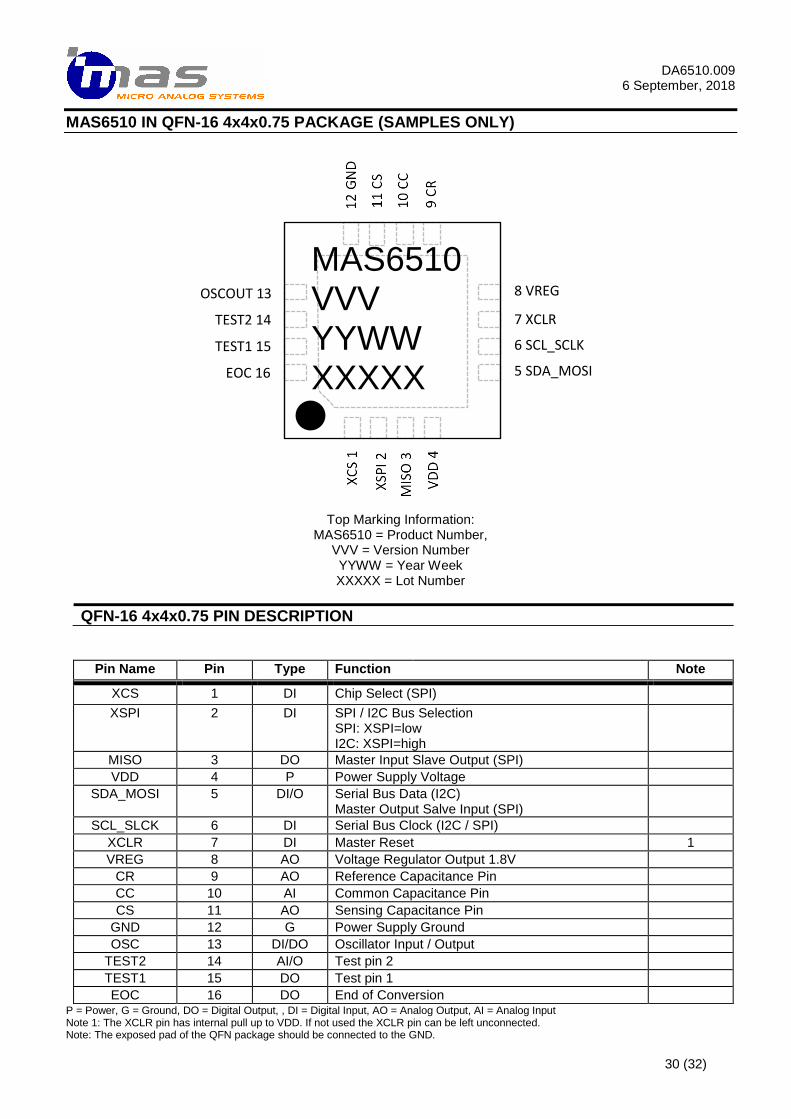
MAS6510 IN QFN-16 4x4x0.75 PACKAGE (SAMPLES ONLY)
Top Marking Information:
MAS6510 = Product Number, VVV = Version Number YYWW = Year Week XXXXX = Lot Number
QFN-16 4x4x0.75 PIN DESCRIPTION
Pin Name Pin Type Function Note
XCS 1 DI Chip Select (SPI)
XSPI 2 DI SPI / I2C Bus Selection SPI: XSPI=low I2C: XSPI=high
MISO 3 DO Master Input Slave Output (SPI)
VDD 4 P Power Supply Voltage
SDA_MOSI 5 DI/O Serial Bus Data (I2C) Master Output Salve Input (SPI)
SCL_SLCK 6 DI Serial Bus Clock (I2C / SPI)
XCLR 7 DI Master Reset 1
VREG 8 AO Voltage Regulator Output 1.8V
CR 9 AO Reference Capacitance Pin
CC 10 AI Common Capacitance Pin
CS 11 AO Sensing Capacitance Pin
GND 12 G Power Supply Ground
OSC 13 DI/DO Oscillator Input / Output
TEST2 14 AI/O Test pin 2
TEST1 15 DO Test pin 1
EOC 16 DO End of Conversion P = Power, G = Ground, DO = Digital Output, , DI = Digital Input, AO = Analog Output, AI = Analog Input Note 1: The XCLR pin has internal pull up to VDD. If not used the XCLR pin can be left unconnected. Note: The exposed pad of the QFN package should be connected to the GND.
EOC 16
TEST1 15
TEST2 14
OSCOUT 13 8 VREG
7 XCLR 6 SCL_SCLK 5 SDA_MOSI
MAS6510
VVV
YYWW XXXXX
DA6510.009
6 September, 2018
31 (32)
D/2
E/2
SEATINGPLANEA
1
SIDE VIEW
TOP VIEW
D2
D2/2
E2/2
E2
b
BOTTOM VIEW
D
A3
PIN 1 MARK AREA
A
EXPOSED PAD
SHAPE OF PIN #1 IDENTIFICATION IS OPTIONAL
L
DETAIL A
Terminal Tip
Package Center Line X or Y
e
e/2
DETAIL A
PACKAGE (QFN-16 4x4x0.75) OUTLINE (SAMPLES ONLY)
Symbol Min Nom Max Unit
PACKAGE DIMENSIONS
A 0.700 0.750 0.800 mm
A1 0.000 0.020 0.050 mm
A3 0.203 REF mm
b 0.250 --- 0.350 mm
D 3.950 4.000 4.050 mm
D2 (Exposed.pad) 2.700 --- 2.900 mm
E 3.950 4.000 4.050 mm
E2 (Exposed.pad) 2.700 --- 2.900 mm
e 0.650 BSC mm
L 0.350 --- 0.450 mm
Dimensions do not include mold or interlead flash, protrusions or gate burrs.
DA6510.009
6 September, 2018
32 (32)
ORDERING INFORMATION
Product Code Product Description
MAS6510EA1WAD00 Capacitive Sensor Signal Interface IC Tested inked wafer, thickness 370 µm
MAS6510EA1WAD05 Capacitive Sensor Signal Interface IC Bare die in tray, thickness 370 µm
MAS6510EA1WAB05 Capacitive Sensor Signal Interface IC Bare die in tray, thickness 180 µm
MAS6510EA1Q1708 Capacitive Sensor Signal Interface IC QFN-16 4x4x0.75, Pb-free, RoHS compliant, loose components (samples only)
Contact Micro Analog Systems Oy for other wafer and die thickness options and volume orders in QFN package.
LOCAL DISTRIBUTOR
MICRO ANALOG SYSTEMS OY CONTACTS
Micro Analog Systems Oy Kutomotie 16 FI-00380 Helsinki, FINLAND
Tel. +358 10 835 1100 http://www.mas-oy.com
NOTICE Micro Analog Systems Oy (MAS) reserves the right to make changes to the products contained in this data sheet in order to improve the design or performance and to supply the best possible products. MAS assumes no responsibility for the use of any circuits shown in this data sheet, conveys no license under any patent or other rights unless otherwise specified in this data sheet, and makes no claim that the circuits are free from patent infringement. Applications for any devices shown in this data sheet are for illustration only and MAS makes no claim or warranty that such applications will be suitable for the use specified without further testing or modification. MAS products are not authorized for use in safety-critical applications (such as life support) where a failure of the MAS product would reasonably be expected to cause severe personal injury or death. Buyers represent that they have all necessary expertise in the safety and regulatory ramifications of their applications, and acknowledge and agree that they are solely responsible for all legal, regulatory and safety-related requirements concerning their products and any use of MAS products in such safety-critical applications, notwithstanding any applications-related information or support that may be provided by MAS. Further, Buyers must fully indemnify MAS and its representatives against any damages arising out of the use of MAS products in such safety-critical applications. MAS products are neither designed nor intended for use in military/aerospace applications or environments. Buyers acknowledge and agree that any such use of MAS products which MAS has not designated as military-grade is solely at the Buyer's risk, and that they are solely responsible for compliance with all legal and regulatory requirements in connection with such use. MAS products are neither designed nor intended for use in automotive applications or environments. Buyers acknowledge and agree that, if they use any non-designated products in automotive applications, MAS will not be responsible for any failure to meet such requirements.