Embed Size (px)
Citation preview

Capacitive Displacement Sensing for the Nanogate by
Hongshen Ma
B.A.Sc. University of British Columbia (2001)
Submitted to the Program in Media Arts and Sciences, School of Architecture and Planning,
In partial fulfillment of the requirements for the degree of
Masters of Science in Media Arts and Sciences
at the
MASSACHUSETTS INSTITUTE OF TECHNOLOGY
February 2004
© Massachusetts Institute of Technology 2004. All rights reserved.
Author__________________________________________________________________ Program in Media Arts and Sciences
January 15, 2004
Certified by______________________________________________________________ Joseph A. Paradiso
Associate Professor Sony Career Development Professor of Media Arts and Sciences
MIT Program in Media Arts and Sciences
Accepted by_____________________________________________________________ Andrew Lippman
Chair, Department Committee on Graduate Students MIT Program in Media Arts and Sciences

2

Abstract The Nanogate is a micro electro mechanical systems (MEMS) device that uses a
cantilever structure to control the separation between two extremely flat surfaces. It has
been proposed that the Nanogate be used as part of a nanoscale instrument for studying
the behavior of fluids at the molecular scale. This thesis describes the development of an
integrated capacitive displacement sensor which enables nanometer precision
measurement of the separation of the surfaces of the Nanogate.
The work in this thesis can be divided into two parts: fabrication of a new version
of the Nanogate and the development of electronics for the capacitive sensor. The
fabrication part involved redesigning the Nanogate package and fabrication process to
integrate the capacitive sensing electrodes, as well as to improve the process yield. The
development of capacitive sensing electronics for the Nanogate involved the design of an
analog front-end to convert capacitance to voltage and a custom high precision data
acquisition system to digitize the output.
The measured capacitance is converted back to absolute displacement by
calibration with a Michelson interferometer-based displacement sensor. The results show
a resolution better than 0.1nm and the long term drift error is less than 1nm.
3

4

Capacitive Displacement Sensing for the Nanogate by
Hongshen Ma
The following people served as readers for this thesis:
Thesis Reader____________________________________________________________ Joseph A. Paradiso
Associate Professor Sony Career Development Professor of Media Arts and Sciences
MIT Program in Media Arts and Sciences
Thesis Reader____________________________________________________________ Alexander H. Slocum
Professor MacVicar Faculty Fellow
MIT Department of Mechanical Engineering
Thesis Reader____________________________________________________________ Scott R. Manalis
Assistant Professor NEC Career Development Professor of Computers and Communications
MIT Program in Media Arts and Sciences
5

6

Acknowledgements To my supervisor, Joe Paradiso, for bringing me to the lab, for helping me to
grow as an engineer and as a person, for having the understanding to let me take on this
project, and for supporting me until the very end. You taught me to be relentless in quest
for the answer; and then you taught me about humility and kindness in everything else.
To you I am deeply indebted.
To Alex Slocum for always being optimistic, for treating his students like family,
and for always making research fun.
To Scott Manalis for the early discussions in the Silicon Biology class.
To James White for teaching me everything I know about MEMS fabrication.
To Ari Benbasat for being a great friend and for working with me on my writing
every step of the way.
To Stacy Morris for always bringing a smile to the lab.
To Mat Laibowitz for his help with the microprocessor work and for being a
messy, but wonderful officemate.
To the Responsive Environments Group for making the lab a great place to
work and play.
To Kurt Broderick, Gwen Donahue, and the rest of MTL staff for their
generous help with the fabrication process.
To Kaity Ryan for the last minute corrections.
To the Natural Sciences and Engineering Research Council of Canada for their
financial support.
Finally, to my parents and my best friend, Chris Qually, for reminding me to
work hard even when I didn’t want to and for always having faith in me along the way.
7

8

Table of Contents Abstract ............................................................................................................................... 3
Acknowledgements............................................................................................................. 7
Table of Contents................................................................................................................ 9
List of Figures ................................................................................................................... 11
List of Tables .................................................................................................................... 13
1 Introduction............................................................................................................... 15
1.1 Basic Principle .................................................................................................. 15
1.2 Key Characteristics of the Nanogate................................................................. 17
1.3 Previous work ................................................................................................... 18
1.4 Thesis Goals and Specifications ....................................................................... 19
2 Displacement Sensor Design .................................................................................... 21
2.1 Displacement Sensing Modalities..................................................................... 21
2.2 Choice of Displacement Sensing Strategy........................................................ 23
2.3 Capacitive Sensor Design ................................................................................. 24
3 Fabrication ................................................................................................................ 27
3.1 Mask Design and Fabrication Process Overview ............................................. 27
3.2 Detailed Fabrication Process............................................................................. 29 3.2.1 Materials and Preparation ......................................................................... 29 3.2.2 Photolithography....................................................................................... 30 3.2.3 Deep Reactive Ion Etching ....................................................................... 30 3.2.4 Bottom Side Processing and Oxide Strip.................................................. 31 3.2.5 Metal Deposition....................................................................................... 31 3.2.6 Pyrex Wafer Processing............................................................................ 32 3.2.7 Anodic Bond and Diesaw ......................................................................... 32
3.3 Fabrication Results............................................................................................ 33
4 Circuit Design ........................................................................................................... 37
4.1 Capacitive Sensing Front-end ........................................................................... 37 4.1.1 Input Amplifier ......................................................................................... 37 4.1.2 Synchronous Detector............................................................................... 40 4.1.3 Output Signal Conditioning ...................................................................... 40
9

4.1.4 Switched Calibration................................................................................. 41
4.2 Data Acquisition System................................................................................... 41 4.2.1 Analog to Digital Conversion ................................................................... 42 4.2.2 MSP430 Microprocessor .......................................................................... 42 4.2.3 Visual Basic Data Logger and User Interface........................................... 43
4.3 Physical Circuit Considerations........................................................................ 45 4.3.1 Electrical Contact to Capacitive Electrodes.............................................. 45 4.3.2 Printed Circuit Board Design and Layout................................................. 45
5 Results and Discussion ............................................................................................. 49
5.1 Capacitance versus Displacement..................................................................... 49
5.2 Noise Analysis .................................................................................................. 53
5.3 Drift Analysis.................................................................................................... 55
5.4 Overall Error Budget......................................................................................... 59
6 Conclusion and Future Work .................................................................................... 61
6.1 Conclusion ........................................................................................................ 61
6.2 Future Work ...................................................................................................... 62
Bibliography ..................................................................................................................... 63
Appendix A: Nanogate Masks .......................................................................................... 65
Appendix B: Detailed Fabrication Process ....................................................................... 69
Appendix C: Circuit Diagrams and PCB Layout.............................................................. 73
Appendix D: MSP430 Microprocessor Code ................................................................... 78
Appendix E: Visual Basic Data Acquisition Program...................................................... 82
Appendix F: Matlab Data Analysis and Graphing Code .................................................. 89
10

List of Figures Figure 1: Cross section of the Nanogate with Added Capacitive Sensor Electrodes ....... 16
Figure 2: CAD model of the Nanogate silicon diaphragm ............................................... 16
Figure 3: Cut-away diagram of the capacitive sensing electrodes. The silicon diaphragm is offset from the Pyrex diaphragm................................................................................... 25
Figure 4: Nanogate die 3D model. Left: topview, Halo’s are used to reduce etching time. Right: bottom view, a trench is designed to accommodate the capacitive electrodes on the Pyrex. ................................................................................................................................ 27
Figure 5: Capacitive electrode mask for the Pyrex wafer................................................. 28
Figure 6: Outline of the Nanogate fabrication process, wafer shown in cross-section..... 29
Figure 7: Metal Deposition on Silicon Wafer (not to scale)............................................. 32
Figure 8: Profilometer scan of the silicon valveland showing 2nm rms surface roughness............................................................................................................................................ 34
Figure 9: SEM Micrograph of the silicon diaphragm after the fulcrum is deliberately broken from the anodic bond with the Pyrex wafer.......................................................... 35
Figure 10: Profilometer scan of the Pyrex wafer after bonding. The reflow of the Pyrex wafer can be seen conforming to the shape of the silicon valveland. The remains of the fulcrum can be seen at the corners.................................................................................... 35
Figure 11: SEM of the Pyrex surface after bonding. The faint circle shows the indentation made by the silicon during the anodic bonding process. .................................................. 36
Figure 12: Capacitive sensing front-end ........................................................................... 37
Figure 13: Input amplifier in high and low impedance configuration .............................. 38
Figure 14: Input Amplifier Schematic .............................................................................. 39
Figure 15: Level shifter and 4-pole VCVS low-pass filter ............................................... 41
Figure 16: Switched calibration circuit............................................................................. 41
Figure 17: Data Acquisition System................................................................................. 42
Figure 18: Screen-shot of the Visual Basic data collection and user interface program .. 44
Figure 19: Electrical connection between capacitive electrodes and input amplifier....... 45
Figure 20: Photograph of the analog front-end PCB ........................................................ 47
11

Figure 21: Photograph of the data acquisition PCB showing split ground planes for the ADC (left side) and microprocessor (right side)............................................................... 47
Figure 22: Actuator command versus time....................................................................... 50
Figure 23: Capacitance output in ADC counts versus time.............................................. 51
Figure 24: Zygo output versus time .................................................................................. 51
Figure 25: Zygo vs. Capacitance divided into 3 regions .................................................. 52
Figure 26: Residue plot of Zygo vs. Capacitance minus its linear fit line in region III of Figure 25 ........................................................................................................................... 52
Figure 27: Noise waveform from the output filter and bandgap reference....................... 54
Figure 28: Noise waveform of the full differential capacitive sensing circuit ................. 54
Figure 29: Drift from bandgap reference and output filter ............................................... 56
Figure 30: Temperature dependence of drift from bandgap reference and output filter .. 56
Figure 31: System output without calibration................................................................... 57
Figure 32: Temperature dependence of drift .................................................................... 57
Figure 33: System output with calibration showing less than 1nm drift .......................... 58
Figure 34: System output with calibration in the presence of external disturbances........ 58
Figure 35: Mask for the Nanogate wafer bottom side (color inverted) ............................ 65
Figure 36: Mask for the Nanogate wafer top side (color inverted)................................... 66
Figure 37: Mask for the Nanogate Pyrex base.................................................................. 67
Figure 38: Analog front-end full schematic...................................................................... 73
Figure 39: Data acquisition circuit full schematic ............................................................ 74
Figure 40: Analog front-end PCB layout, top layer.......................................................... 75
Figure 41: Analog front-end PCB layout, bottom layer ................................................... 75
Figure 42: Data acquisition PCB layout, top layer ........................................................... 76
Figure 43: Data acquisition PCB layout, bottom layer ..................................................... 77
12

List of Tables Table 1: Modalities for nanoscale displacement sensing.................................................. 23
Table 2: Overall error budget............................................................................................ 59
13

14

1 Introduction The study of the physical properties of fluids at the molecular scale has gathered
considerable research interest. Numerous studies have shown that as the sample size is
reduced, bulk models often break down, yielding to a regime where the molecular nature
of the fluid must be considered [1-4]. As these studies converge to the length scale of an
individual molecule, which is on the order of nanometers, there is a need for instruments
that can confine and measure materials at this new level of precision.
The Nanogate is a micro electro mechanical systems (MEMS) device that uses a
cantilever structure to control the separation between two ultra-flat surfaces. Using
MEMS materials and processing techniques, it is possible to fabricate devices with
nanometer-scale smooth surfaces. It is therefore possible to build a tunable gap with
nanometer order size and precision. In a gap from a few to tens of nanometers wide, it is
hypothesized that fluid can enter a regime where molecular behavior dominates over bulk
behavior [1-4]. Consequently, the Nanogate could form the basis of an instrument to 1)
study the mobility of molecules in a fluid as a way to separate the species of interest; or
2) measure the electrical response of molecules as a means of identifying the species of
interest.
The work in this thesis is intended to be an initial step towards this nanometer
scale instrument by developing a displacement sensor to accurately measure the size of
the nanometer gap. Specifically, this involves fabricating a new version of the Nanogate
and developing the necessary electronic instrumentation to produce a digital readout that
can be used for servo control.
1.1 Basic Principle Professor Alexander Slocum and James White at MIT’s Mechanical Engineering
Department initially conceived the concept of the Nanogate [5-7]. The Nanogate is
fabricated at MIT’s Microsystems Technology Laboratory (MTL) using photolithography
and surface micromachining techniques. Its basic structure consists of a disc-shaped
silicon diaphragm assembled together with a Pyrex diaphragm that forms a circular lever-
15
fulcrum structure, where the size off the center gap can be varied by applying a force to
the outer edge.
Metal layers to prevent anodic bond
C
Tunable nanometer gap
500 um Pyrex 7740 base
300 um heavily dopedSi
Torsional springs
C
Zygo measurement beam
Applied Deflection
Fluid inletBottom electrode Anodic Si-Pyrex bond
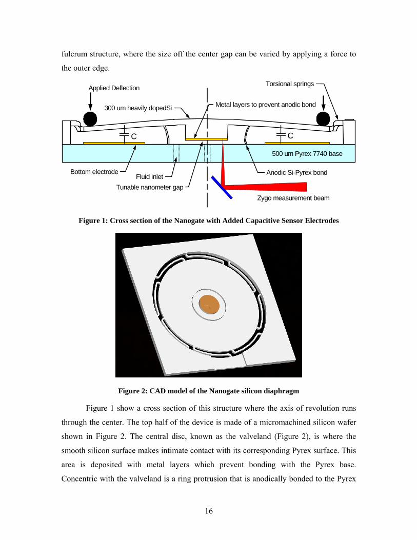
Figure 1: Cross section of the Nanogate with Added Capacitive Sensor Electrodes
Figure 2: CAD model of the Nanogate silicon diaphragm
Figure 1 show a cross section of this structure where the axis of revolution runs
through the center. The top half of the device is made of a micromachined silicon wafer
shown in Figure 2. The central disc, known as the valveland (Figure 2), is where the
smooth silicon surface makes intimate contact with its corresponding Pyrex surface. This
area is deposited with metal layers which prevent bonding with the Pyrex base.
Concentric with the valveland is a ring protrusion that is anodically bonded to the Pyrex
16

glass to form a circular fulcrum. When a force is applied to the outer edge of the silicon
disc, the flex of the fulcrum determines the mechanical transmission ratio from outer
edge to the valveland. This mechanical advantage serves to magnify the mechanical
impedance of the central valveland, and similarly, precision control of gap. Flexible
spring elements are also machined into the silicon diaphragm to hold the disc in place
during the fabrication process.
1.2 Key Characteristics of the Nanogate The structure of the Nanogate yields several important characteristics. First, the
surface roughness of standard silicon and Pyrex wafers is 2-3 nanometers and can be
reduced to less than 0.3 nanometers through specialized polishing techniques. By
preserving this surface finish throughout the fabrication process, it is possible to produce
a true, parallel nanometer gap. As additional evidence will show, the anodic bonding
process causes the Pyrex wafer to reflow to the shape of the silicon layer, making the two
surfaces complementary to each other.
Second, the gap is adjustable with a large dynamic range, from a few nanometers
to micrometers. This property can be used in a precision fluid control system where the
flow rate can be precisely tuned. Furthermore, when clogging occurs in a small channel,
the valve can be opened a large amount to flush the channel.
Third, the stiffness of single crystalline silicon and the silicon-to-Pyrex anodic
bond give the valveland region tremendous mechanical impedance. This is further
magnified by the mechanical transmission provided by the lever-fulcrum structure. As a
result, it is possible to control the gap distance independent of materials and surface
forces in the gap.
Fourth, the design of the Nanogate allows for a large lateral dimension relative to
the gap dimension. This provides a large surface area to volume ratio for chromatography
applications where it is beneficial to maximize the interaction between the fluid and
channel surfaces.
Finally, the Pyrex-silicon chamber formed by anodic bond is vacuum tight, which
means that the Nanogate could be used as a valve in gas applications where a vacuum
17

seal is required. In fact, it has been shown that the Nanogate device has one of the lowest
helium-leak rates among available microvalves [7].
1.3 Previous work James White designed the original structure of the Nanogate and developed a
process to fabricate these devices at MTL as part of his Ph.D. work [7]. The original
design has a 1.5mm diameter valveland and 2.25mm diameter fulcrum. The outer
diameter of the disc is 7.5mm and the designed transmission ratio from the deflection of
the outer edge to the gap is 15:1. The entire silicon die is a 10 x 10 mm square fabricated
on a 100 mm diameter silicon wafer. The individual dies are separated using a diesaw and
then bonded to a Pyrex base of the same dimensions.
In the fall of 2001, White and Ma designed an experimental fixture to test the
initial version of the Nanogate. The Nanogate is actuated through a spring flexure using a
piezoelectric motor. The piezoelectric motor drove a lead screw that advanced in
submicron steps. The displacement of the center region is measured using a commercial
Michelson interferometer made by Zygo [8]. These experiments showed controlled
displacement of the center region in 2.4nm steps [9].
Although the original device and experiment showed great promise, there are
several problems that hinder its ability to achieve nanometer control of the gap size. The
Zygo interferometer used to measure displacement had drift problems on the order of
100nm per hour, which makes impractical to use for feedback control on the nanometer
level. Additionally, the Zygo is bulky and expensive instrument that would be impractical
for widespread use.
Another problem is the unreliable results produced from the original fabrication
process. Since the silicon and Pyrex diaphragm are bonded as individual dies rather than
entire wafers, the wafers had to be cut before proceeding with the anodic bond. Particles
from the diesawing process often contaminated the bonding surfaces and drastically
reducing the yield of successful devices. Furthermore, even before the diesaw, the bond
surfaces are often already contaminated in the previous micromachining step where
photoresist is an insufficient masking material.
18

1.4 Thesis Goals and Specifications The goal of this work is to develop a displacement sensor to allow the Nanogate
to more accurately and easily measure the size of the gap at the valveland. The
specifications include measurement of the gap size to better than 1nm with long term drift
error less than 1nm. In addition to providing a more accurate measurement, this
displacement sensor must also be compatible with fluid based experiments and
mechanically integrateable with the Nanogate’s external actuator. This development
process involves first deciding on a displacement measurement strategy, then fabricating
a new version of the Nanogate that integrates the features necessary for measurement,
and finally developing the supporting instrumentation that can provide an electronic
readout. Compared to the bulky interferometer used previously, a simpler and more
compact measurement system is desired.
The development of the displacement sensor for the Nanogate initially involves
choosing a sensing strategy. This process is described in Chapter 2 and concludes with
the decision to use capacitive sensing. Next, an improved fabrication process, designed to
incorporate the capacitive sensor, is presented in Chapter 3. This chapter also includes the
characterization of the fabricated components. The development of electronics for
measuring capacitance sensing is discussed in Chapter 4. This section includes
descriptions of the capacitive sensing front end, analog signal conditioning, precision
data acquisition system, and the computer control interface as well as the PCB design.
Results from the capacitive displacement sensing are presented in Chapter 5 along with
analysis of noise and drift in the system. This thesis concludes in Chapter 6 where
possible improvements on the system and future work are discussed.
19

20

2 Displacement Sensor Design This section begins with a presentation of the displacement sensing modalities
appropriate for measuring position with nanometer accuracy. Then, the strengths and
weaknesses of each sensor are weighed in the context of sensing for the Nanogate.
Finally, a detailed design of the capacitive displacement sensor for the Nanogate is
presented.
2.1 Displacement Sensing Modalities A variety of sensing modalities are available to measure position with nanometer
resolution including techniques that measure optical intensity, optical phase, capacitance,
magnetic field, and piezoelectric response. Piezoelectric sensors [10, 11] are quickly
dismissed because of poor repeatability and excessive temperature sensitivity; Magnetic
field sensors [11] are also eliminated because of susceptibility to interference and
difficulty in integration into the Nanogate fabrication process. The others merit further
examination.
Optical intensity-based displacement sensors measure the change in amplitude of
a light beam reflected off the target of interest. The most accurate of this type of sensor
reflects off the target at an angle and then uses a CCD array to triangulate the position of
the reflected spot. By assuming a Gaussian beam and then interpolating between CCD
elements, sub-wavelength accuracy can be achieved. Keyence sells a commercial version
of this displacement sensor with 10nm resolution with 20 kHz bandwidth [12].
Optical phase based position sensors use a laser source to generate a diffraction
pattern. The change in the diffraction pattern as a function of position can then be
measured using a photodetector. Two realizations of this general technique are the
Michelson interferometer and interdigitated diffraction gratings. The Michelson
interferometer uses light from a laser source and divides it into two beams. Each beam
travels a separate path and is reflected back via a retro-reflector to recombine and form a
standing wave interference pattern. Usually, the path length of one beam is fixed and is
21

considered to be the reference path while the path length of the other beam is variable and
is considered to be the measurement path. The phase of the interference pattern is
depended on the phase difference of the two paths. By measuring the amplitude at a
specific point along the interference pattern it is possible to determine the displacement to
a fraction of the wavelength of the source. Zygo makes a commercial version of this
instrument where displacement can be measured with up to 2.4nm resolution at 4 kilo-
samples-per-second [8]. An optional attachment of this instrument allows the
measurement beam to be focused off a planar reflector target instead of using a retro-
reflector [13]. This configuration is used to measure displacement in the first incarnation
of the Nanogate where the beam is focused through the Pyrex base at the valveland. One
of the problems with this setup is that the measurement is non-differential. It is prone to
thermal drift in the mechanical structure, which is measured to be on the order of 100nm
per hour [9].
Interdigitated diffraction gratings use two gratings offset by half of their period to
form a grating with double the frequency. The grating is excited by a laser source, which
forms a diffraction pattern. Moving gratings out of plane with respect to each other
modulates the antinodes of the odd and even harmonic in the diffraction pattern. Using a
split photodiode pair to measure the difference over sum of the adjacent antinodes, it is
then possible to measure the motion of the gratings with extreme precision. Manalis et al
have shown displacement measurements with resolution down to 0.002 nanometers with
a 1kHz bandwidth [14, 15].
Capacitive sensors electronically measure the capacitance between two or more
electrodes and convert this value to a displacement [16-19]. The usual technique involves
exciting the measurement capacitor at a high frequency and then measuring its impedance
response. The high frequency excitation reduces the impedance of the capacitor to a
manageable range and the response signal is down-converted to a DC voltage. Capacitive
sensors are used extensively for position sensing in MEMS devices. Perhaps one of the
most successful commercial products is the ADXL series accelerometers from Analog
Devices, which use capacitance to measure the motion of a tethered proof mass. The
ADXL series devices uses entirely integrated electronics and have demonstrated better
than 0.002 nanometer resolution position sensing with a bandwidth of 10 kHz [18, 20].
22

2.2 Choice of Displacement Sensing Strategy
Method Resolution Drift Bandwidth Integration Requirements
Laser intensity – triangulation with CCD [12]
10 nm 40 nm/C 20 kHz Optical path to the Nanogate
Michelson interferometer [8, 13]
2.4 nm 100 nm/hr 20 kHz Optical path to the Nanogate
Interdigitated gratings [14, 15] 0.002 nm N/A 1 kHz Optical path to the Nanogate and
fabricated grating features.
Capacitive measurement [18, 20]
0.002 nm N/A 10 kHz Two electrodes and wire connection
Table 1: Modalities for nanoscale displacement sensing
Resolution, drift, and ease of integration with the Nanogate are considered in
choosing the displacement sensing technology. Table 1 summarizes the relevant
specifications of the different sensing modalities. The target resolution is 1nm, at 100Hz
bandwidth, with less than 1nm/hour of drift.
The intensity-based position sensor is dismissed due to lack of resolution. The
Zygo interferometer has borderline acceptable resolution, but the nature of this
measurement scheme also leads to problems with drift. Additionally, the Zygo is a bulky
and expensive setup and not practically for wide use of the Nanogate.
The interdigitated diffraction grating sensor is an intriguing possibility because it
is a true differential measurement. However, in order to integrate this sensing scheme,
gratings must be embedded in the Pyrex at some fixed depth away from the Pyrex-silicon
interface. This is a challenging task as well-controlled etching of Pyrex is not an
established technique at MTL.
The capacitive sensors can be designed with extremely high resolution and would
be simple to integrate with the Nanogate. Therefore, it is the choice of displacement
sensing for this work. The disadvantage of capacitive sensing is that it is difficult to
translate a change in capacitance to an absolute displacement. This difficulty arises due
the presence of stray coupling of electric fields (e.g. stray capacitance), which is a
23

difficult parameter to model and predict in a complicated geometry such as the Nanogate
with external connections. Therefore, a calibration routine is necessary to determine the
capacitance to displacement mapping.
2.3 Capacitive Sensor Design The most straightforward approach to Nanogate displacement sensing via
capacitance would have been to put electrodes on either sides of the gap. However, the
impedance measurement would depend on the dielectric and conductive properties of the
liquid or gas in the gap. To avoid this problem, the capacitive measurement is made at the
outside edge of the cantilever, with the silicon diaphragm as one electrode and a gold
trace deposited on the Pyrex as the other electrode (Figure 3). It is assumed that
deflection around the outside edge has a single-valued and stable mapping to the
movement of the valveland. This is a reasonable assumption because a single crystal
silicon wafer has no mechanism for creep. The mapping of the outer edge to center
deflection, however, cannot be exactly determined a priori, because processing variations
in the silicon disc produce uncertainties in the thickness of the fulcrum and strength of
the anodic bond. Therefore, the Zygo interferometer is used to calibrate the capacitance
versus displacement function for each Nanogate.
To a first order approximation, the electrostatic coupling between the outer edge
of the silicon diaphragm and gold trace on the Pyrex die can be modeled as a parallel
plate capacitor, such that
dA
C 0ε= , (1)
where A is the area of the electrodes, d is the spacing of the electrodes, and ε0 is
the permittivity of free space. For small plate deflections, the capacitance varies as,
dd
AC ∆−=∆ 20
0ε , (2)
where d0 is the initial undeflected distance and ∆d is the displacement caused by
the external deflection.
The initial separation of the outer edge of the silicon diaphragm is approximately
150µm with a total expected travel of 15µm. This means that the capacitance will vary up
24

to 10% of the value at the undeflected state. The total area of the electrode pattern is
approximately 24.5mm2, resulting in an undeflected capacitance of approximately
1.45pF. With a target of better than 1 nm resolution at the center, it is necessary to
measure capacitance with accuracy better than 0.3 femto farad or a signal-to-noise ratio
of 74dB. The measurement resolution will be ultimately limited by noise and drift. By
using synchronous detection as a measurement technique these parameters can be
reduced.
It is important to note that the desired measurement accuracy (1nm) is obtainable
even though the Zygo interferometer calibration is less accurate (2.4nm). This result is
achieved by fitting the calibration data with a line regression, which has a sufficiently
accurate gradient.
Figure 3: Cut-away diagram of the capacitive sensing electrodes. The silicon diaphragm is offset from the Pyrex diaphragm
25

26

3 Fabrication This chapter describes the fabrication of the Nanogate from the design of the
mask to a detailed description of the microfabrication process using the MEMS tools at
Microsystems Technology Laboratory. The chapter concludes with a presentation of the
fabrication results.
3.1 Mask Design and Fabrication Process Overview The basic structure of the Nanogate, as described in Section 1.1, is a part of a
larger silicon die designed to support electrical contact and fluid connections as shown in
Figure 4, at the left. The main disc of the Nanogate occupies the top-left quadrant of the
die. On the bottom side of the die (Figure 4, at the right), a rectangular trench runs from
the disc area to one of the holes to house the capacitive electrode. The other two holes are
designed as fluid inlet and outlet, and the window at the top-right quadrant is designed for
observing fluid channels. Since the development of the capacitive measurement system
does not require active fluid connections, these features are not used.
Figure 4: Nanogate die 3D model. Left: topview, Halo’s are used to reduce etching time. Right: bottom view, a trench is designed to accommodate the capacitive electrodes on the
Pyrex.
27

The Pyrex die is patterned with the capacitive electrode and aligns with the silicon
die. As described in section 2.3, the electrode is a ring around the outside edge of the disc
with an electrical contact inside the trench (Figure 3). In the future, when fluids are
introduced into the Nanogate, the Pyrex die will be machined with additional features as
microchannels and through-holes.
The silicon diaphragm and its corresponding Pyrex diaphragm are batch
processed on wafers. Each wafer can hold a total of 14 dies with appropriate alignment
and die-saw features. The silicon wafer is fabricated using two surface micromachining
steps, one at the top surface and another at the bottom surface. One mask is required for
each side. The masks are generated from a cross section of an assembly drawing of the
dies. The larger through features are removed using halos to reduce the amount of etching
necessary. A third mask is designed to pattern the Pyrex wafer with the electrode pattern
in Figure 5.
Figure 5: Capacitive electrode mask for the Pyrex wafer
28

3.2 Detailed Fabrication Process This section outlines the detailed fabrication process for the Nanogate. Figure 6
shows an outline of the process flow.
Silicon Oxide Resist Metal Pyrex
1) Grow thermal oxide
2) Spin coat photoresist,pattern by photolithography
4) DRIE silicon for 150 um
5) Flip over wafer, pattern backside as 2 and 3
6) DRIE silicon for another 150 um until through
7) Deposit Ti-Au on top side as electrical contact. Deposit Ti-Pt-Ti-Au using a shadowmask on the valveland to prevent anodic bond.
8) Deposit Ti-Au on Pyrex substrate using standard lift-off process
9) Anodic bond of silicon and Pyrex wafer. Metal layers at the valveland prevent the bond, and lightly preloads the fulcrum
3) Coat the bottom with photoresist, etch the exposed oxide using BOE
Figure 6: Outline of the Nanogate fabrication process, wafer shown in cross-section.
3.2.1 Materials and Preparation The wafers used for this fabrication process are low resistivity (0.008 Ω-cm) n-
type silicon wafers with specifications of 100mm in diameter, 300µm (±25µm) thick, and
polished smooth on both sides. The preparations for photolithography involve cleaning
the wafers using standard RCA clean and then thermally growing a 1µm silicon dioxide
layer on the surface. The SiO2 layer acts as a “hard mask” to preserve the pristine surface
finish of the silicon wafer during the surface micromachining process. Previously, only
photoresist had been used as a masking material and the micromachining process often
contaminated the silicon surfaces and prevented proper anodic bonding.
29
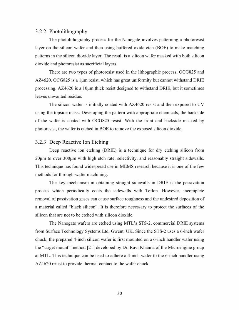
3.2.2 Photolithography The photolithography process for the Nanogate involves patterning a photoresist
layer on the silicon wafer and then using buffered oxide etch (BOE) to make matching
patterns in the silicon dioxide layer. The result is a silicon wafer masked with both silicon
dioxide and photoresist as sacrificial layers.
There are two types of photoresist used in the lithographic process, OCG825 and
AZ4620. OCG825 is a 1µm resist, which has great uniformity but cannot withstand DRIE
processing. AZ4620 is a 10µm thick resist designed to withstand DRIE, but it sometimes
leaves unwanted residue.
The silicon wafer is initially coated with AZ4620 resist and then exposed to UV
using the topside mask. Developing the pattern with appropriate chemicals, the backside
of the wafer is coated with OCG825 resist. With the front and backside masked by
photoresist, the wafer is etched in BOE to remove the exposed silicon dioxide.
3.2.3 Deep Reactive Ion Etching Deep reactive ion etching (DRIE) is a technique for dry etching silicon from
20µm to over 300µm with high etch rate, selectivity, and reasonably straight sidewalls.
This technique has found widespread use in MEMS research because it is one of the few
methods for through-wafer machining.
The key mechanism in obtaining straight sidewalls in DRIE is the passivation
process which periodically coats the sidewalls with Teflon. However, incomplete
removal of passivation gases can cause surface roughness and the undesired deposition of
a material called “black silicon”. It is therefore necessary to protect the surfaces of the
silicon that are not to be etched with silicon dioxide.
The Nanogate wafers are etched using MTL’s STS-2, commercial DRIE systems
from Surface Technology Systems Ltd, Gwent, UK. Since the STS-2 uses a 6-inch wafer
chuck, the prepared 4-inch silicon wafer is first mounted on a 6-inch handler wafer using
the “target mount” method [21] developed by Dr. Ravi Khanna of the Microengine group
at MTL. This technique can be used to adhere a 4-inch wafer to the 6-inch handler using
AZ4620 resist to provide thermal contact to the wafer chuck.
30

The front side pattern is etched to a nominal depth of 150µm, but the actual etch
depth is between 170 and 190µm to account for etch non-uniformities across the wafer.
Non-uniformities can be reduced by rotating the wafer to several different orientations
during the course of the recipe. The alignment marks are etched separately for a short
duration and then covered with a small drop of AZ4620. After the desired depth has been
reached, the wafer is first cleaned in oxygen plasma to remove any leftover Teflon. Then,
it is Piranha cleaned to remove the photoresist and separate the Nanogate wafer from its
handler.
3.2.4 Bottom Side Processing and Oxide Strip After the desired patterns have been obtained on the top side of the Nanogate, a
similar process is used to pattern the bottom side starting from the photolithography step.
An additional alignment step is required to line up the front side patterns with the
backside mask. The DRIE depth for the bottom side is approximately 150µm, with the
etch completion gauged by the completion of the through features.
When features on both sides of the wafer have been completed, the silicon dioxide
masking layer can be removed using 49% Hydrogen Fluoride (HF). Another Piranha
clean is necessary following the oxide etch to make a thin layer of native oxide, which
helps to keep the wafer clean after it is taken out of solution.
3.2.5 Metal Deposition Both sides of the micromachined silicon wafer are deposited with metals using
electron-beam deposition. The top side of the wafer is deposited with titanium and gold
layers that act as electrical contacts to the silicon die. The gold layer is responsible for
reducing the contact resistance caused by the native oxide on the silicon, while titanium
layer is an adhesion layer for the gold.
On the bottom side, 4 layers of metal are deposited over the valveland designed to
prevent anodic bond in the region (Figure 7). Starting from the bare silicon, the
deposition sequence consists of titanium, platinum, titanium, and gold at thicknesses of
20nm, 100nm, 20nm, and 100nm. The gold layer, with no native oxide, is the primary
deterrent of anodic bond. During the thermal cycles of the bonding process, however, the
gold layer diffuses away from the silicon-glass interface and forms a eutectic with the
31

silicon, allowing anodic bonding to proceed. Therefore, a platinum layer is necessary to
add a diffusion barrier between the gold and silicon layers. The titanium layers are
included as adhesion layers between the silicon-platinum and platinum-gold interfaces.
Titanium
TitaniumPlatinum
Gold
TitaniumGold
Silicon
Electrical Contact
Anodic bondPrevention
Figure 7: Metal Deposition on Silicon Wafer (not to scale)
3.2.6 Pyrex Wafer Processing The wafers used to make the Pyrex substrate are 700µm thick, 100mm diameter
Borofloat glass wafers from Mark Optics [22]. Processing on the Pyrex wafer involves
photolithography and liftoff processes to deposit a pattern of metal traces that can be
aligned with the silicon wafer. The Pyrex wafer is prepared using a Piranha clean and
then coated with OCG825 photoresist. The wafer is then exposed with the electrode
pattern shown in Figure 5 and developed. Similar to the silicon wafer, the Pyrex wafer is
deposited with titanium as an adhesion layer and gold as the electrode. The final result is
obtained by using acetone with ultrasound agitation to liftoff the metal deposited on top
of the photoresist mask.
3.2.7 Anodic Bond and Diesaw Anodic bonding is a process that joins silicon to Pyrex glass by applying a high
voltage across the joint at the appropriate temperature and pressure. The positive
electrode is connected to the silicon while the negative electrode is place to the Pyrex
side. As the voltage is applied across the junction, Na+ ions in the Pyrex glass migrate
away from the junction and O- ions migrate towards the junction. The O- ions oxidizes
the silicon at the interface to form a strong covalent bond between the Pyrex and silicon.
The anodic bond between the Nanogate’s silicon and Pyrex wafers are made at
the wafer level using the EV501 aligner/bonder. Prior to the bonding process, the wafers
32

are rinsed in a sequence of acetone, methanol, isopropanol, and de-ionized water.
Subsequently, the wafers are dried in the SRD spinner. Using the EV501 aligner, the
wafers are carefully aligned and clamped together. The bonder recipe calls for 800V at
350°C and 1000 Newtons for approximately 30 minutes.
After the bond process has been completed, the excess sodium ions on the back of
the Pyrex wafer are washed off using de-ionized water. Subsequently, the wafer is sliced
into 20mm by 20mm dies according to the die-saw marks etched into the wafer.
In previous versions of this process, the anodic bond is made at die level after the
silicon and Pyrex wafers had been diesawed individually. The resulting bond is often
unreliable because of the particles introduced to the silicon and Pyrex surfaces by the
diesawing process.
3.3 Fabrication Results A few of the completed silicon-Pyrex dies have been deliberately broken to
analyze the quality of the silicon and Pyrex surfaces at the valveland. The instruments
used for this task are the scanning electron microscope (SEM) and the whitelight
profilometer.
Figure 8 is a profilometer scan of the silicon surface measuring the roughness
variations. It can be seen that less than 5nm peak-to-peak surface roughness has been
preserved on the valveland surface. Figure 9 shows a SEM micrograph of the silicon
diaphragm after the fulcrum has been deliberately is broken. When the silicon diaphragm
is broken from the Pyrex diaphragm, almost a full ring of the fulcrum remained bonded to
the Pyrex. This means the anodic bond is actually stronger than the fulcrum itself.
33

Figure 8: Profilometer scan of the silicon valveland showing 2nm rms surface roughness.
Figure 10 is a profilometer scan of the Pyrex surface after the silicon diaphragm is
removed. The ring protrusion is an indentation made by the silicon valveland during the
anodic bonding. The thermal cycle of the anodic bond brings the Pyrex wafer to a
temperature where it reflows and conforms to the shape of the silicon diaphragm. This is
an favorable result since the Pyrex wafer has inherently worse surface roughness than
silicon, but the anodic bonding process can modify the Pyrex surface to produce mating
silicon and Pyrex surfaces. Figure 11 shows a similar result as Figure 10 in a SEM
micrograph.
34

Figure 9: SEM Micrograph of the silicon diaphragm after the fulcrum is deliberately broken from the anodic bond with the Pyrex wafer
Figure 10: Profilometer scan of the Pyrex wafer after bonding. The reflow of the Pyrex wafer can be seen conforming to the shape of the silicon valveland. The remains of the
fulcrum can be seen at the corners.
35

Figure 11: SEM of the Pyrex surface after bonding. The faint circle shows the indentation made by the silicon during the anodic bonding process.
36

4 Circuit Design This chapter describes the electronic circuits associated with the capacitive
measurement system’s readout electronics. The analog front-end that converts
capacitance to a voltage is described in Section 4.1, followed by the data acquisition
system used to digitize the signal in Section 4.2. Finally, the physical implementations of
these two subsystems are discussed in Section 4.3. Full schematics, printed circuit board
layout, and accompanying software programs are included in the appendices.
4.1 Capacitive Sensing Front-end The analog front-end converts capacitance to a voltage by exciting the Nanogate
capacitor using an AC signal and using analog electronics to measure the electrical
response to the signal. The circuitry for this task can be separated into three stages: an
input amplifier to buffer the signal from the capacitor, a synchronous detector to mix the
signal to DC, and an output filter to remove the out-of-band noise and to shift the output
voltage to within range of the ADC (Figure 12) [18].
C110 kHzSine
+1
-1
LPF
AD630
ADC
Sync Signal
Input Amplifier
HPF
Figure 12: Capacitive sensing front-end
4.1.1 Input Amplifier The purpose of the input amplifier is to measure the impedance of the Nanogate
capacitor C1 with the least amount of signal degradation caused by parasitic capacitance,
37

parasitic resistance, and noise. Parasitic capacitance attenuates the response to the
measured capacitance and is mainly found between the capacitive sensing electrode and
the printed circuit board (PCB), as well as between the input pin and other pins of the
amplifier. Modeled as parallel to the capacitor of interest, the parasitic capacitance
reduces the measured signal and may vary with time, temperature, and humidity.
Parasitic capacitance can be minimized by using guard electrodes around the input that
are bootstrapped to the input voltage (dotted lines in Figure 13). Parasitic resistance refers
to the leakage current through the input of the amplifier. Its effects on the signal are
similar to those of parasitic capacitance. In addition to the use of guard electrodes,
parasitic resistance can be minimized by thoroughly cleaning the PCB using flux remover
and by choosing amplifiers that are specifically designed for low input bias current.
Cref+
-
Rlarge
+
-
High ImpedanceNon-Inverting Configuration
Low ImpedanceInverting Configuration
CrefCnanogate
Cnanogate
Figure 13: Input amplifier in high and low impedance configuration
There are two fundamental circuit topologies for detecting signal from a
capacitive sensor: using a high impedance input to measure voltage and using a low
impedance input to measure current (Figure 13). In the high impedance (non-inverting)
case, the Nanogate capacitor is a part of a capacitive divider, and the input of the
amplifier moves with the voltage of the signal. In the low impedance (inverting) case, the
input of the amplifier is at a virtual ground and a reference capacitor is used in feedback;
the capacitively coupled current is converted into a voltage by a transimpedance
amplifier. The low impedance configuration is chosen over the high impedance
configuration because the full excitation signal can be applied to the Nanogate capacitor
compared to only half in the high impedance configuration. Additionally, since the input
38

of the amplifier is a virtual ground in the low impedance configuration, the operating
point of the amplifier is constant, and therefore less prone to common-mode errors.
The OPA129 [23] operational amplifier is chosen as the input amplifier because it
offers extremely low input bias current of 100fA maximum. Its minimum unity-gain
bandwidth is 0.7MHz, which provides a loop gain of 70 at 10kHz excitation. The input-
referred noise at 10kHz is specified at 15nV/(Hz)-½ voltage noise and 0.1fA/(Hz)-½
current noise.
The input amplifier circuit is shown in Figure 14. C1 is the Nanogate capacitor,
and C2 is a reference capacitor of approximately the same value as C1. R1, R2, and R3
form a resistive T-network to provide a high impedance DC path to ensure that the
inverting input does not float to arbitrary voltages.
2
1
CC
VV
in
out = , if CR
ffb
excitation π21
>> , (3)
where Rfb is the equivalent parallel resistance to C2. The T-network formed by R1,
R2, and R3 reduces the feedback to the input by the ratio of R2/R3 and, consequently,
magnifies the effective parallel resistance to C2 by the same factor. An effective parallel
resistance of 500MΩ is achievable, far beyond the value that can be realized using
conventional components. The resulting time constant of the feedback loop is
approximately 100Hz, which satisfies the condition of equation 3 for a fexcitation of 10kHz.
The disadvantage of the T-network is that the offset of the input amplifier is also
multiplied by the same ratio as the feedback resistance. Therefore, output of the input
amplifier is AC coupled to the next stage to eliminate errors caused by offset drift.
C2
+
-
Cstray
+
-
C1
R1 R2
R3
OPA129
Vout
10 kHzSine
Figure 14: Input Amplifier Schematic
39

4.1.2 Synchronous Detector Synchronous detection is a signal conditioning technique designed to detect the
amplitude of a fixed-frequency signal in the presence of noise. In this scheme the
measured signal is multiplied with a reference signal of the same frequency and phase.
The amplitude of the desired signal is therefore transformed down to DC, while low
frequency noise is transformed up to the reference frequency. The output of the multiplier
can then be low-pass filtered to remove the noise at the reference frequency and beyond.
The multiplier that follows the input amplifier is the AD630 precision modulator
from Analog Devices [24]. The AD630 has two parallel amplifiers with gains of +1 and -
1, and switches the output between the two amplifiers at the frequency of the reference
signal. This has the effect of multiplying the input signal with a square wave at the
reference frequency, and it is insensitive to amplitude of the reference signal. Figure 12
shows the simplified schematic of the AD630 where the input signal is the output of the
OPA129 and the reference signal comes from a TTL gate derived from the 10kHz
sinusoidal source.
4.1.3 Output Signal Conditioning The output of the AD630 is level shifted and low-pass filtered before being
digitized by an ADC. The level shift moves the DC level of the output to a voltage range
acceptable for the ADC, and is implemented using a LT1007 operational amplifier [25] in
an inverting configuration with unity gain (Figure 15). The amount of shift is determined
by the voltage at the non-inverting terminal, which is set by a LT1019 bandgap reference
[26] followed by a voltage divider.
The low-pass filter removes out-of-band signals from synchronous detection and
sets the total system bandwidth. A four-pole voltage-controlled voltage-source (VCVS)
filter is implemented using two LT1007 operational amplifiers (Figure 15) [27, 28]. This
filter has a bandwidth of 160 Hz and a total gain of 2.5.
40

Vin+
-
LT1007
Vout
+
-
LT1007
+
-
LT1007
LT1019 10V Bandgap
RD1
RD2
RD0
RF2
C
RIN
RD0 RD2
RF1
RIN
C
RIN
RD1 = 5.90k
RF1
RF2
C
RD0
RF1
RF2
C
= 39.2k
= 48.7k= 10.0k= 10.0k
= 10.0kC = 0.1uf Cutoff = 160 Hz
Gain = 2.5
Figure 15: Level shifter and 4-pole VCVS low-pass filter
4.1.4 Switched Calibration The long-term variation in the offset of the AD630 and the output stage is
calibrated using a switched reference source at the input of the AD630 (Figure 16). At
periodic instances a reference signal is switched into the AD630 and its result is stored
and used as the overall system offset. The reference signal is generated using an identical
OPA129 input amplifier where the Nanogate has been replaced by a reference capacitor.
The switch is implemented using an AD451, a low on-resistance analog switch.
C110 kHzSine +1
-1
LPF
AD630
ADC
Calibration Signal
InputAmplifier
HPF
CrefReference Amplifier
AD451
Sync Signal
Figure 16: Switched calibration circuit
4.2 Data Acquisition System A custom data acquisition system is designed to digitize the output of the analog
section. The three main components of this system include a high resolution ADC, a
41

microprocessor, and a computer. A temperature sensor is also included to measure signal
drift as a function of temperature. The analog input is digitized by the ADC and read by
the microprocessor, which also measures input from the temperature sensor and controls
the Nanogate’s external actuator. The capacitance and temperature data from the
microprocessor and the displacement data from the Zygo interferometer are logged by a
Visual Basic program on the computer.
ADCMSP430
Microprocessor Computer:Visual Basic
Program
RS232
To Actuator
Analog Differential
Input
Internal ADC
Temperature Sensor
From Zygo Interferometer
RS232SPI
Figure 17: Data Acquisition System
4.2.1 Analog to Digital Conversion Voltage output from the analog front-end is digitized using a LTC2440 ADC from
Linear Technology [29]. The LTC2440 is a differential input with a 2.5V range and 24
bits digital output. The maximum sampling rate is 4 kilo-samples-per-second (ksps) but is
settable to allow the user to exchange resolution for bandwidth. On this particular data
acquisition board, the LTC2440 is set to sample at 1 ksps, which corresponds to an
effective resolution of 114 dB, significantly more than the required 74 dB.
4.2.2 MSP430 Microprocessor The functions of the microprocessor include reading data from the ADC,
measuring temperature, controlling the Nanogate’s external actuator, and relaying data to
the computer. The MSP430 microprocessor series from Texas Instruments is chosen
because of its programmability. Specifically, the MSP430F149 [30] is used. It has 60
kilobytes of flash program memory, an internal 12-bit ADC, 2 timers, and can be clocked
42

up to 8MHz. The microprocessor communicates with the ADC over a 3-wire SPI
interface.
The temperature is measured using an AD592 temperature dependent current
source [31]. The AD592 sources current proportional to absolute temperature at a ratio of
1 uA/K. The output current is converted to voltage via a resistor and digitized using the
MSP430’s 12-bit internal ADC. The measured temperature resolution is 0.125°C.
The Nanogate actuator is controlled via several digital lines provided by the
MSP430. These signals include clock, step command, and direction. Since the actuator
takes in 5V TTL signals and the MSP430 runs at 3.3V, a Schmidt-triggered inverter is
used as an interface.
The MSP430 communicates with the computer via a serial line at 57.6 kbits/s.
The internal UART of the MSP430 is connected to a RS-232 line driver, which is
connected to a computer using a standard 9-pin serial connector.
4.2.3 Visual Basic Data Logger and User Interface Capacitance, temperature, and displacement from the Zygo interferometer are
read by a Visual Basic program (Figure 18), which stores the data on disk and provides a
real-time stripchart display. This program is also allows the user to send commands to
control the external actuator via the microprocessor. The actuator motion can be
controlled by single commands or a script that automatically performs motion (up, down,
and wait) sequences.
43

Figure 18: Screen-shot of the Visual Basic data collection and user interface program
44

4.3 Physical Circuit Considerations 4.3.1 Electrical Contact to Capacitive Electrodes
The capacitive electrodes on the silicon and Pyrex part of Nanogate are connected
to the analog front-end via thin, flexible copper wires (Figure 19). The wires are bonded
by conductive epoxy [32] to the electrodes on the Nanogate and are soldered to pads on
the printed circuit board. The wires are single strands taken from standard 26 gauge
stranded wire.
Thin copper wire
Silver EpoxyInput Amplifier
Nan
ogat
e
Figure 19: Electrical connection between capacitive electrodes and input amplifier
4.3.2 Printed Circuit Board Design and Layout The analog front-end and data acquisition circuits are implemented on standard 2-
layer, 62 mil, FR-4 printed circuit boards (PCB). The two circuits are made on separate
boards in order to minimize interference between the two circuits and to modularize the
development effort. The signal lines between the two PCBs are connected via SMA-type
45

coaxial cable, which provide a shielded electrical connection with a flexible mechanical
connection.
Ground planes are used extensively on the two PCBs to reduce the interference
caused by external electromagnetic fields. All components are placed on the top of the
circuit board so that a complete ground plane can be formed on the bottom side of the
PCB. The data acquisition PCB has separate ground planes between the ADC and the
microprocessor section of the board in order to reduce the effect of digital noise on the
ADC. The two PCBs are also enclosed in a grounded metal box for shielding against
external interference signals.
Power on the two circuit boards are supplied via several voltage regulators to
minimize the interference coupled through the power supply. The analog front-end is
supplied +12V and -12V rails for its analog components. A dedicated 5V digital rail is
provided for the logic supply on the analog switch. The data acquisition circuit board is
powered with a 5V analog line for the LT2440 ADC and temperature sensor, a 5V digital
line for driving the picomotor actuator, a 3.3V analog rail for the ADC onboard the
microprocessor, and a 3.3V digital rail for digital functions on the microprocessor.
The placement of components and signal lines on the circuit board is also given
careful consideration. Every effort is made to keep the length of signal lines as short as
possible and components that can add noise to the signal line, such as digital logic gates,
are deliberately placed farther away.
After the components are soldered onto the board, the PCBs are cleaned
extensively with flux-remover to clear away the leftover flux residue. Since the DC
impedances on the circuit board range from 10-500 MΩ, the electrical conduction of flux
can be a significant parasitic.
Figure 20 and Figure 21 are photographs of the analog front-end and data
acquisition PCBs. The detailed schematic and PCB layout are shown in Appendix C.
46

Figure 20: Photograph of the analog front-end PCB
Figure 21: Photograph of the data acquisition PCB showing split ground planes for the ADC (left side) and microprocessor (right side)
47

48

5 Results and Discussion This chapter presents the results from testing the capacitive displacement sensor.
Section 5.1 describes the results of the capacitance versus displacement measurement.
Section 5.2 analyzes the noise floor of the capacitance measurement. Finally, section 5.3
examines the drift error of the capacitance measurement.
5.1 Capacitance versus Displacement As discussed in section 2.3, each Nanogate device needs to be calibrated using the
Zygo interferometer. As external deflection is applied to the silicon diaphragm, the data
acquisition software records the value of the ADC from the capacitive measurement
circuit, displacement as measured by the Zygo interferometer, and the room temperature.
In order to minimize drift in the Zygo readings caused by air currents, the laser beam is
shielded using acrylic tubes. Figure 22 shows the sequence of actuator deflections, Figure
23 shows the response of the capacitive sensor, and Figure 24 shows the response of the
Zygo interferometer. The droop of the capacitance and Zygo output after each set of input
steps is an artifact of the actuator assembly: The force on the silicon diaphragm is applied
through an o-ring, which has a relatively slow relaxation time.
Figure 25 shows the calibration of Zygo measured displacement versus
capacitance. This graph has three distinct regions. In region I, the capacitance is
increasing in response to the deflection from the actuator while the central valveland
remains fixed. This is because the deflection of the outer edge must first overcome the
preload due to the additional thickness of the metal film layer that causes the diaphragm
to bend during the anodic bonding. Region III shows the valveland displacement varying
as a linear function of capacitance as in equation (2). Region II is the non-linear,
transition between regions I and III. It is hypothesized that this transition region is caused
by asymmetry in the actuation of the outer edge of the silicon diaphragm and with better
actuation schemes the rounded region can be reduced. The roundedness of this region
makes it difficult to define a zero point. It is possible to interpolate this point by fitting a
straight line to region III in Figure 25 and finding its intercept with the mean of region I.
49

Figure 26 shows the Zygo versus capacitance plot subtracted from its linear fit
line in region III of Figure 25. A periodic fine structure, on the order of 5nm, is revealed
and consistent during both the opening and the closing of the Nanogate. The source of
this behavior is likely an artifact of the actuator and how it interacts with the mounting
structure, however, more analysis is necessary to fully understand this problem.
Figure 22: Actuator command versus time
50

Figure 23: Capacitance output in ADC counts versus time
Figure 24: Zygo output versus time
51

Figure 25: Zygo vs. Capacitance divided into 3 regions
Figure 26: Residue plot of Zygo vs. Capacitance minus its linear fit line in region III of Figure 25
52

5.2 Noise Analysis Noise is inherent to all electronic systems and fundamentally limits measurement
resolution. Noise can be classified by its spectral response as stray pickup, white noise,
and 1/f noise. 1/f noise is considered as part of drift and will be discussed in the next
section.
Stray pickup is the coupling of interference signals from sources near the circuit
such as microprocessors, CRTs, and power lines. In the design of the capacitive sensor,
stray pickup is minimized by careful layout of the printed circuit board. These
considerations include surrounding all signal lines with ground planes, using separate
power supplies and ground planes for analog and digital circuits, and shielding the entire
circuit in a grounded metal box. Since stray pickup cannot be easily predicted, it is
measured experimentally along with white noise.
White noise has a flat spectral density and its integral over the total system
bandwidth represents the output amplitude. In passive dissipative elements, namely
resistors, the source for white noise is attributed to Johnson or thermal noise; in active
elements, the source for white noise is attributed to shot noise. White noise is minimized
by the choice of appropriate passive and active devices. In the capacitive sensing analog
front-end circuit, white noise can be calculated by summing the specified noise power of
each device and integrating it over the total bandwidth, which is set by the bandwidth of
the output filter at 160Hz.
The circuit elements that contribute to white noise are the OPA129 input
amplifier, AD630, LT1019 bandgap reference, and the three LT1007 amplifiers that
make up the level shifter and output filter. The noise from the bandgap reference, level-
shifter and output amplifier can be measured separately by disconnecting the input from
the AD630. Figure 27 shows a noise waveform measured using the LTC2440 ADC,
where the RMS variation is 5.6µV and a peak-to-peak variation of approximately 30µV
The noise band of interest for the OPA129 and AD630 is centered at 10 kHz with
a bandwidth of 320 Hz. The bandwidth is doubled due to the frequency conversion in the
synchronous detection process. The measured noise of the entire analog front-end is
shown in Figure 28, where the RMS variation of 37µV or equivalently 0.056nm, and a
peak-to-peak variation of 200µV or 0.3nm. Practically, the expected resolution can be
53

taken as an average of the RMS and peak-to-peak value at 0.2nm. As a matter of
reference this is equivalent to 0.1 femto farad of capacitive change.
Figure 27: Noise waveform from the output filter and bandgap reference
Figure 28: Noise waveform of the full differential capacitive sensing circuit
54

5.3 Drift Analysis Drift is the variation in system output over long periods of time and is caused by
variations on circuit parameters such as resistance, amplifier offset, and circuit gain. The
causes of these variations include temperature, humidity, and slow relaxation processes in
the circuit elements and on the circuit board. The function blocks that affect output drift
are the bandgap reference, the output filter, the AD630, and input amplifier.
Figure 29 and Figure 30 shows the output drift and temperature dependence from
only the bandgap reference and the output filter. The results are stable to within 0.05nm,
smaller the noise floor of the analog front-end circuit. Shown in Figure 31 and Figure 32,
drift from AD630 is significantly higher and temperature dependent. Using the
calibration scheme discussed in Section 4.1.4, this drift can be compensated to within
1nm of variation (Figure 34) in a span of 20 hours. Figure 34 shows drift at the output in
the presence a lot of external disturbances due to activity in the lab. The calibration is
able to compensate most of the variation, but the peak-to-peak variation due to drift is
now 2nm. This result shows that in order to minimize drift, careful consideration must be
give to shielding and environmental control around the measurement system.
Offset variation in the OPA129 does not cause drift at the output because the
signal from the OPA129 is AC coupled into the AD630. However, variation in gain
between the input and reference amplifiers also causes output drift and cannot be
corrected under the current calibration scheme. One way to solve this problem is to
switch in a reference capacitor in parallel with the Nanogate. This scheme presents
additional difficulties as settling time for the switching transients may become an issue.
It is important to note that the gain of the input and reference amplifiers operate
under extremely high impedance and is sensitive to parasitic conduction on the PCB and
therefore, the cleanliness of the PCB. In future monolithic implementations where the
entire circuit can be enclose in a hermetically sealed package, this issue may be
drastically improved.
55

Figure 29: Drift from bandgap reference and output filter
Figure 30: Temperature dependence of drift from bandgap reference and output filter
56

Figure 31: System output without calibration
Figure 32: Temperature dependence of drift
57

Figure 33: System output with calibration showing less than 1nm drift
Figure 34: System output with calibration in the presence of external disturbances
58

5.4 Overall Error Budget Table 2 shows the overall error budget of the system with an expected resolution
of 0.2nm and long-term drift within 2nm.
Source Measured noise
RMS
Measured noise
peak-to-peak
Expected resolution
(RMS+PP)/2
Noise 0.056nm 0.3nm 0.2nm
Drift 1nm 1nm 1nm
Table 2: Overall error budget
59

60

6 Conclusion and Future Work
6.1 Conclusion The objective of this work is to develop a displacement measurement system for
the Nanogate with better than 1nm resolution and long-term stability with at least 100 Hz
system bandwidth. The Nanogate is a circular cantilever structure that allows the precise
control of the separation between ultra-flat silicon and Pyrex surfaces to form a tunable
nanometer gap.
Several displacement sensing strategies are considered including techniques based
on measuring optical intensity, optical phase, and capacitance. The capacitive technique
is chosen for its ease of mechanical integration with the Nanogate and the capability to
achieve high measurement resolution. To make the capacitive displacement sensing
compatible with future fluid flow applications, the capacitive electrodes are placed at the
outer edge of the circular silicon diaphragm and at the corresponding region on the Pyrex
base. A Zygo interferometer displacement sensor can then be used to determine the
mapping between capacitance and displacement of the gap.
A new version of the Nanogate is fabricated that incorporates the capacitive
electrodes. The processing yield is increased by using silicon dioxide “hard” mask during
DRIE and incorporating wafer level bonding into the fabrication process.
Electronics for capacitive sensing is developed to convert capacitance in the
Nanogate to a voltage and then to a digital value. An analog front-end printed circuit
board is designed and built that uses synchronous detection to produce a voltage output
for the corresponding capacitance. A custom data acquisition system is developed to
accurately digitize this voltage. The result is transmitted via serial line to a computer
where the data is stored and graphed by a Visual Basic program. In order preserve the
accuracy of the measurement, careful layout considerations are made in both circuit
boards and a calibration scheme is introduced to reduce drift in the system.
In the final system, the Nanogate capacitance is found to vary linearly with
displacement once the silicon and Pyrex surfaces are separated. The residue plot shows a
61

periodic fine structure on the order of 5nm, but more analysis is necessary to understand
its physical origin.
The noise and drift of this measurement system has been optimized and tested.
The expected resolution is 0.2nm with a system bandwidth of 160 Hz and an expected
long-term drift of lnm. The goals set out at the beginning of this thesis have been met,
although careful consideration must be given to shielding and environmental control
around the measurement system.
6.2 Future Work In addition to adding an improving the calibration scheme discussed in the
previous section, the next steps in obtaining true nanometer control of the gap separation
is to develop a better actuator. Some of the basic requirements include better than
nanometer open-loop resolution and the ability to apply a uniform force around the
perimeter of the silicon diaphragm. An integrated actuator using piezoelectric material
may have fewer packaging requirements and therefore be an attractive option. This work
may be complemented by adding quadrant capacitive electrodes to measure uneven
deflections on the silicon diaphragm.
The first application of the Nanogate will be for a portable gas transfer standard
for the National Institute of Standards and Technology (NIST). This work will involve
incorporating the improved sensor and actuator with gas tight fluid connections and
calibrating the values of capacitance with a flow rate measured by a highly sensitive mass
spectrometer.
One of the long-term goals of the Nanogate is the use the controllable nanometer
gap as a tool for studying molecular behavior in highly confined spaces. This would
require the nanometer gap to be filled with liquid, which means that the transfer function
between capacitance at the outer edge and gap length will be dependent on the
mechanical properties of the fluid in the gap. As result, this capacitive sensing geometry
will probably not be feasible and a more direct sensing geometry is necessary. This could
possibly involve mounting a capacitive electrode some distance away from the center of
the silicon diaphragm.
62

Bibliography 1. Chen, D.Y.C. and R.G. Horn, The drainage of thin liquid films between solid
surfaces. J. Chem. Phys., 1985. 83(10): p. 5311-5323.
2. Demirel, A.L. and S. Granick, Origins of solidification when a simple molecular fluid is confined between two plates. J. Chem. Phys., 2001. 115(3): p. 1498-1512.
3. Zhu, Y. and S. Granick, Rate dependent slip of Newtonian liquid at smooth surfaces. Phys. Rev. Lett., 2001. 87(9, 27).
4. Zhu, Y. and S. Granick, Limits of the hydrodynamic no-slip boundary condition. Phys. Rev. Lett., 2002. 88(10,11).
5. Slocum, A.H., Method of and apparatus for substance processing with small opening gates actuated and controlled by large displacement menbers having fine surface finishing. 1999: US.
6. White, J.R., et al., An instrument to control parallel plate separation for nanoscale flow control. Review of Scientific Instruments, 2003. 74(11).
7. White, J.R., The Nanogate: Nanoscale Flow Control. Ph.D. Thesis, in Mechanical Engineering. 2003, Massachusetts Institute of Technology.
8. Zygo ZMI-1000.
9. Ma, H. and J. White, Packaging and Initial Characterization of the Nanogate. 2001, Massachusetts Institute of Technology, MAS.962 final report: Cambridge.
10. APC International, www.americanpiezo.com.
11. Fraden, J., Handbook of Modern Sensors: Physics, Designs, and Applications. 2 ed. 1997: springer Verlag.
12. Keyence laser displacement sensor: http://www.keyence.com/products/measuring/lc/lc_spec.html.
13. Zygo ZMI optical probe accessory manual, OMP-0238B.
14. Yaralioglu, G.G., et al., Analysis and design of an interditial cantilever as a displacement sensor. J. Appl. Phys., 1998. 12(83): p. 7405-7415.
15. Manalis, S.R., et al., Interditial cantilevers for atomic force microscopy. Appl. Phys. Lett., 1996. 69(25): p. 3944-3946.
63

16. Puers, B., Capacitive sensors: when and how to use them. Sensors and Actuators, 1993. A37-A38: p. 93-105.
17. Jones, R.V. and J.C.S. Richards, The design and some applications of sensitive capacitance micrometers. Journal of Physics E: Scientific Instruments, 1973. 6: p. 589-600.
18. Baxter, L., Capacitive Sensors: Design and Applications. IEEE Press Series on Electronics Technology. 1996: IEEE.
19. Paradiso, J.A., New technologies for monitoring the precision alignment of large detector systems. Nuclear Instruments and Methods in Physics Research A., 1997. 386: p. 409-420.
20. ADXL50 datasheet: http://www.analog.com/UploadedFiles/Obsolete_Data_Sheets/2044696ADXL50.pdf, Analog Devices.
21. Khanna, R. 2003.
22. Mark Optics. www.markoptics.com
23. OPA129 datasheet: http://www-s.ti.com/sc/ds/opa129.pdf, Texas Instruments.
24. AD630 datasheet: http://www.analog.com/UploadedFiles/Data_Sheets/129044951AD630_d.pdf, Analog Devices.
25. LT1007 Datasheet: http://www.linear.com/pdf/100737fb.pdf, Linear Technology.
26. LT1019 datasheet: http://www.linear.com/pdf/1019fcs.pdf, Linear Technology.
27. Lancaster, D., Active Filter Cookbook. 2nd ed. 1995, Thatcher, AZ: Synergetics Press.
28. Horowitz, P. and W. Hill, The Art of Electronics. 2nd ed. 1989: Cambridge University Press.
29. LTC2440 datasheet: http://www.linear.com/pdf/2440f.pdf, Linear Technology.
30. MPS430F149 datasheet: http://www-s.ti.com/sc/ds/msp430f149.pdf, Texas Instruments.
31. AD592 datasheet: http://www.analog.com/UploadedFiles/Data_Sheets/136700329AD592_a.pdf, Analog Devices.
32. Tra-Duct 2902 Silver Epoxy, www.tra-con.com/products/tpb.asp?product=2902, Tra-Con.
64

Appendix A: Nanogate Masks
Figure 35: Mask for the Nanogate wafer bottom side (color inverted)
65

Figure 36: Mask for the Nanogate wafer top side (color inverted)
66

Figure 37: Mask for the Nanogate Pyrex base
67

68

Appendix B: Detailed Fabrication Process Hongshen Ma
Created: December 29, 2002, Updated: July 15, 2003
[email protected] Meta
Description Description Lab Machine Recipe Diagram
4”, 500um heavily doped Si wafer. N-type, Sb doping, resistivity = 0.008 ohm-cm
Silicon Oxide Resist Gold Pyrex
RCA ICL RcaTRL SOP
Preparation and Oxidation
Oxidation ICL Tube5D-fieldox
Grow 1um oxide, 1050 C, 200 min
HMDS TRL HMDS Recipe 3
Deposit thick resist TRL Coater 10um, AZ4620, 1500rpm
Prebake TRL Prebake 90°C, 60min Expose TRL EV1 Expose 30s
Develop TRL Photo Wet AZ440 2minutes per wafer
Rinse TRL Dump rinse 5min Dry TRL SRD 4”
Coat backside TRL Coater 1um, OCG825, 3000rpm
Postbake TRL Postbake 90°C, 30min Remove oxide TRL Acid-hood BOE 16 minutes
Mount on 6” quartz carrier wafer TRL Coater Target mount, AZ4620
1800 rpm
Top side pattern and etch
Alignment mark etch TRL STS-2 13s
69

Cover alignment mark TRL photoroom Use AZ4620 and q-tip
bake for 5min
DRIE TRL STS-2 Etch 170-190um, MIT37A 50 minutes
Remove Teflon TRL Asher 20+ minutes Dismount TRL Acidhood2 Piranha X 2 (or more) HMDS TRL HMDS Recipe 3
Deposit thick resist TRL Coater 10um, AZ4620, 1500rpm
Prebake TRL Prebake 90°C, 60min Expose TRL EV1 Expose 30s
Develop TRL Web bench AZ440 2minutes per wafer
Rinse TRL Dump rinse Dry TRL SRD 4”
Coat backside TRL Coater 1um, OCG825, 3000rpm
Postbake TRL Postbake 90°C, 60min Remove oxide TRL Acidhood BOE 16 minutes
Mount on 6” quartz carrier wafer TRL Coater Target mount,
AZ4620, 1800 rpm Alignment mark etch TRL STS-2 13s
Cover alignment mark TRL photoroom Use AZ4620 and q-tip
bake for 5min
DRIE TRL STS-2 Etch 150um use MIT37A 50 minutes or until through
Remove Teflon TRL Asher 20+ minutes
Bottom side pattern and etch
Dismount TRL Acid-hood Piranha X 2 (or more)
Deposit electrode TRL E-beam 20nm Ti, 100nm Au
Add bond stop layer and metal Mount shadowmask TRL Photo room ***Use a small amount
of AZ4620 resist
70

Bake TRL Prebake 90°C, 10 minutes
Deposit metal TRL E-beam 20nm Ti, 100nm Pt, 20nm Ti, 100nm Au
Acetone dismount TRL Photowet As long as needed
Solvent clean TRL Photowet Methenol and Isopropanol
DI-water clean TRL Dump rinse
contacts
Dry TRL SRD 4” HMDS TRL HMDS Deposit Photoresist TRL Coater 1um OCG825 resist Prebake TRL Prebake 90°C, 30 minutes Exposure TRL EV-1 2s Develop TRL Photo wet AZ440 Postbake TRL Postbake 120°C, 30 minutes
Remove residual resist TRL asher 2 min
Deposit metal TRL eBeamAu 20nm Ti, 80nm Al Liftoff TRL Photo wet Acetone overnight
Solvent clean TRL Photowet Methenol and Isopropanol
DI-water clean TRL Dump rinse
Process for electrical traces on Pyrex base. We use 500um Pyrex 7740 wafer
Dry TRL SRD 4”
Anodic bond Anodic bond TRL EV501-620
325°C, 1000N, 600V–5min, 800V-30min
Diesaw Diesaw ICL diesaw
71

72

Appendix C: Circuit Diagrams and PCB Layout
Figure 38: Analog front-end full schematic
73

Figure 39: Data acquisition circuit full schematic
74

Figure 40: Analog front-end PCB layout, top layer
Figure 41: Analog front-end PCB layout, bottom layer
75
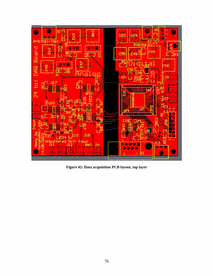
Figure 42: Data acquisition PCB layout, top layer
76

Figure 43: Data acquisition PCB layout, bottom layer
77

Appendix D: MSP430 Microprocessor Code
//***************************************************************** // MSP430F149 interface for LTC2440 ADC // // Hongshen Ma // Created: August 28, 2003 // Last modified: Jan. 20, 2004 //***************************************************************** #include <msp430x14x.h> //#define OSR (0x30000000) // OSR value determines ADC conversion rate //unsigned long int OSRbuf = OSR; // OSR shift register unsigned long int capdata = 0; unsigned long int buf32 = 0; unsigned char buf8=0; unsigned int picostate=0; // 0 waiting for instruction, 1 processing instruction, 2 turning picomotor unsigned int picosteps; // number of steps char picostat='A'; // A no step; B CW step; C CCW step unsigned int picotime=0; // keeps track of timer cycles signed char stepsdone=0; unsigned int tempsense; // 12bit temperature value in Kelvins unsigned int calmode=0; // calibration mode indicator: 0=normal operation, 1=baseline calibration, 2=scalefactor calibration unsigned int calcount=3; //calibration counter, we plan to make a calibration once a minute = every 1200 counts void main(void) unsigned int i; WDTCTL = WDTPW + WDTHOLD; // Stop WDT: required //clock settings BCSCTL1 = XTS + XT2OFF + RSEL0 + RSEL1 + RSEL2; // Enable XT1, disable XT2, highest possible DCO BCSCTL2 = SELM1 + SELM0; // MCLK = XT1, SMCLK=DCO, DCO internal resistors, SMCLK divide by 1 do IFG1 &= ~OFIFG; // Clear OSCFault flag for (i = 0xFF; i > 0; i--); // Time for flag to set while ((IFG1 & OFIFG) != 0); // OSCFault flag still set? //serial communication settings 57600 baud on USART1 //UART1 -> PC U1CTL = CHAR; // 8-bit character UTCTL1 = SSEL0; // UCLK = ACLK U1BR0 = 0x8B; // Set PC UART Baud rate U1BR1 = 0x00; // at 57.6k baud UMCTL1 = 0x00; // no modulation ME2 |= UTXE1 + URXE1; // Enable USART0 TXD/RXD IE2 |= URXIE1; // Enable USART0 RX interrupt P3SEL |= BIT6 + BIT7; // P3.4,5 = USART0 TXD/RXD P3DIR |= BIT6; // P3.4 output direction //internal ADC settings ADC12CTL0 = ADC12ON; // Turn on ADC12, use int. 1.5V reference ADC12CTL1 = ADC12SSEL_2; // Use MCLK for ADCCLK ADC12MCTL0 = INCH_3; // Select input and reference channels P6SEL |= BIT3; // Enable A6 //Port settings for Picomotor driver P4DIR |= BIT0 + BIT1 + BIT2; // BIT0=CLK, BIT1=DIR, BIT2=STEP //Pin settings for LTC2440 ADC //P3.0=_CS; P3.1=SDI; P3.2=SDO; P3.3=SCK; P3.4=BUSY P3DIR |= BIT0 + BIT1 + BIT3; P3OUT = BIT0; P5DIR |= BIT0 + BIT1 + BIT3; P5OUT = BIT0 + BIT1 + BIT2; //TimerA and TimerB settings TACTL = TASSEL0 + TACLR + MC0; // Timer A clocking on ACLK, up count mode, clear interrupt TACTL &= ~TAIFG; TBCTL = TBSSEL0 + TBCLR + MC0 + ID_3; // Timer B use ACLK, clear TAR, upcount mode TBCCTL0 = CCIE; // CCR0 interrupt enabled
78

TBCCR0 = 50000; // Run Timer B at 20Hz _EINT(); // Enable interrupts for (;;) _NOP(); // Required only for C-spy interrupt[TIMERB0_VECTOR] void Timer_B (void) unsigned int i; if (picotime == 1) while (P3IN & BIT4); P3OUT &= ~BIT0; _NOP(); _NOP(); while (P3IN & BIT2); // OSRbuf = OSR; //if we are ready for a calibration we switch over to the calibration input if ((calcount % 150)==0) // First calibration mode P5OUT = BIT0 + BIT1 + BIT2; for (i=1;i<=10;i++); calcount=0; calmode=0; // Here calmode is actually 0 since this result will be ADC'ed in the next round. P5OUT = BIT0 + BIT2; for (i=1;i<=1000;i++); else if (((calcount % 150)>=1) && ((calcount % 150)<=22)) calmode=1; else if ((calcount % 150)==23) P5OUT = BIT0 + BIT1 + BIT2; for (i=1;i<=10;i++); calmode=1; P5OUT = BIT1 + BIT2; else if ((calcount % 150)==24) calmode=1; // We can only report the calibration later because of the 1 data point buffer in the ADC else calmode=0; calcount++; //now we get data from the A/D converter for (i=1;i<=32;i++) P3OUT |= BIT3; _NOP(); //read in data capdata=capdata << 1; buf32 = P3IN & BIT2; capdata |= buf32 >> 2; P3OUT &= ~BIT3; _NOP(); //set speed // P3OUT |= (OSRbuf & 0x80000000) >> 30; // OSRbuf = OSRbuf << 1; P3OUT |= BIT0; // Start next conversion // read from temp sensor ADC12CTL0 |= ADC12SC + ENC; // Sampling open ADC12CTL0 &= ~ADC12SC; // Sampling closed, start conversion while ((ADC12CTL1 & ADC12BUSY) == 1); // ADC12BUSY? tempsense = ADC12MEM0; // get conversion results // finished now transmit data over UART capdata = capdata << 3;
79
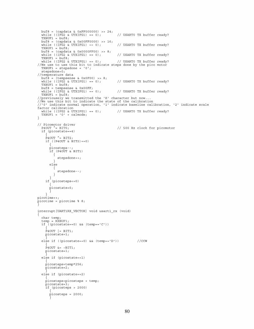
buf8 = (capdata & 0xFF000000) >> 24; while ((IFG2 & UTXIFG1) == 0); // USART0 TX buffer ready? TXBUF1 = buf8; buf8 = (capdata & 0x00FF0000) >> 16; while ((IFG2 & UTXIFG1) == 0); // USART0 TX buffer ready? TXBUF1 = buf8; buf8 = (capdata & 0x0000FF00) >> 8; while ((IFG2 & UTXIFG1) == 0); // USART0 TX buffer ready? TXBUF1 = buf8; while ((IFG2 & UTXIFG1) == 0); // USART0 TX buffer ready? //We use to use this bit to indicate steps done by the pico motor TXBUF1 = stepsdone + '0'; stepsdone=0; //temperature data buf8 = (tempsense & 0x0F00) >> 8; while ((IFG2 & UTXIFG1) == 0); // USART0 TX buffer ready? TXBUF1 = buf8; buf8 = tempsense & 0x00FF; while ((IFG2 & UTXIFG1) == 0); // USART0 TX buffer ready? TXBUF1 = buf8; //previousely we transmitted the 'K' character but now... //We use this bit to indicate the state of the calibration //'0' indicate normal operation, '1' indicate baseline calibration, '2' indicate scale factor calibration while ((IFG2 & UTXIFG1) == 0); // USART0 TX buffer ready? TXBUF1 = '0' + calmode; // Picomotor driver P4OUT ^= BIT0; // 500 Hz clock for picomotor if (picostate==4) P4OUT ^= BIT2; if ((P4OUT & BIT2)==0) picosteps--; if (P4OUT & BIT1) stepsdone++; else stepsdone--; if (picosteps<=0) picostate=0; picotime++; picotime = picotime % 8; interrupt[UART1RX_VECTOR] void usart1_rx (void) char temp; temp = RXBUF1; if ((picostate==0) && (temp=='C')) P4OUT |= BIT1; picostate=1; else if ((picostate==0) && (temp=='D')) //CCW P4OUT &= ~BIT1; picostate=1; else if (picostate==1) picosteps=temp*256; picostate=2; else if (picostate==2) picosteps=picosteps + temp; picostate=3; if (picosteps > 2000) picosteps = 2000;
80

else if (picostate==3) if (temp=='X') picostate=4; else if ((temp=='*') && (picostate==0)) //restart condition CCR0 = 65000; // After synchronization signal wait 15*clk for MSB TACTL |= TACLR; // Timer operation TACTL &= ~TAIFG; // while (!(TACTL & TAIFG)); else picostate=0;
81

Appendix E: Visual Basic Data Acquisition Program Option Explicit Dim holdover As String Dim holdzygo As String Dim recordflag As Boolean Dim numerror As Long Dim capdata As Double Dim tempdata As Double Dim zygodata As Double Dim picodata As Long Dim caldata As String Dim scriptflag1 As Boolean Dim scriptbuf As String Dim command As String Dim cycles As Integer Dim delimiter As Integer Dim savefilename As String Private Sub crc_Click() Dim i As Integer Dim j As Integer Dim crcData As String crcData = "hon" Dim crcReg As Byte Dim databyte As Byte crcReg = 255 Dim CRC8_poly As Byte CRC8_poly = 24 Dim temp As Byte For j = 1 To Len(crcData) databyte = Asc(Mid(crcData, j, 1)) 'or something For i = 1 To 8 If ((crcReg And 128) Xor (databyte And 128)) <> 0 Then temp = crcReg And 128 crcReg = ((crcReg * 2) Mod 256) Xor CRC8_poly Else crcReg = ((crcReg * 2) Mod 256) End If databyte = (databyte * 2) Mod 256 Next Next crcData = crcData + Chr$(crcReg) crcReg = 255 For j = 1 To Len(crcData) databyte = Asc(Mid(crcData, j, 1)) 'or something For i = 1 To 8 If ((crcReg And 128) Xor (databyte And 128)) <> 0 Then crcReg = ((crcReg * 2) Mod 256) Xor CRC8_poly Else crcReg = (crcReg * 2) Mod 256 End If databyte = (databyte * 2) Mod 256 Next Next End Sub Private Sub continuous_Click() continuous.Value = True programmed.Value = False Frame1.Enabled = False Record1.Enabled = True picoframe.Enabled = True End Sub Private Sub Form_Load() Dim temp As String holdover = "" MSComm1.CommPort = 2 MSComm1.Settings = "57600,n,8,1" MSComm1.PortOpen = True MSComm2.CommPort = 1 MSComm2.Settings = "19200,n,8,1" MSComm2.PortOpen = True Timer1.Interval = 50
82

Record1.Enabled = True recordflag = False Frame1.Enabled = False programmed.Value = False continuous.Value = True numerror = 0 picodata = 0 CW.Value = True CCW.Value = False scriptflag1 = False cycles = 0 delimiter = 0 command = "" scriptbuf = "" scriptexample.Caption = "Enter up, down, or wait" + Chr$(13) _ + "plus number of cycles" + Chr$(13) + "each cycle equals 4ms" _ + Chr$(13) + Chr$(13) + "For example:" + Chr$(13) + Chr$(13) _ + "wait 100" + Chr$(13) + "down 50" + Chr$(13) + "wait 100" _ + Chr$(13) + "up 20" + Chr$(13) + "wait 100" logfilelabel.Caption = "Enter path and file name" + Chr$(13) _ + "e.g. c:\data\log1" + Chr$(13) + "3 digit extension added automatically" Call logfilename_Change currentdata.Text = "hello!" Strip1.MaxBufferSize = 1000 Strip1.VariableLastX = 1 Strip1.VariableDeltaX = 1 Strip1.XSpan = 1000 Strip1.ClearAll Strip2.MaxBufferSize = 1000 Strip2.VariableLastX = 1 Strip2.VariableDeltaX = 1 Strip2.XSpan = 1000 Strip1.ClearAll 'MSComm1.Output = "*" 'reset TI microprocessor MSComm1.InputLen = 0 temp = MSComm1.Input MSComm2.InputLen = 0 temp = MSComm2.Input End Sub Private Sub Form_Unload(Cancel As Integer) Dim temp As String MSComm1.InputLen = 0 temp = MSComm1.Input MSComm2.InputLen = 0 temp = MSComm2.Input If recordflag Then Print #3, "/* Halted at " + Str$(Now) + "*/" Close #3 End If MSComm1.PortOpen = False MSComm2.PortOpen = False End Sub Private Sub logfilename_Change() Dim filenumber As Integer Dim ext As String filenumber = 1 ext = "001" Do Until Dir$(logfilename.Text + "." + ext) = "" filenumber = filenumber + 1 ext = Format$(filenumber, "#") If Len(ext) = 1 Then ext = "00" + ext ElseIf Len(ext) = 2 Then ext = "0" + ext End If Loop logfileext.Text = ext savefilename = logfilename.Text + "." + ext End Sub Private Sub MSComm1_OnComm() Dim buf As String Dim i As Integer Dim j As Integer Dim crcReg As Byte
83

Dim databyte As Byte crcReg = 255 Dim CRC8_poly As Byte CRC8_poly = 24 'RECEIVE COMPLETE PACKET Dim Bits As String Dim holdCh As String Dim foostr As String Dim tmpState As Integer Dim DataFound As Boolean Dim holdInt As Integer Dim holdByte As Byte DataFound = False Select Case MSComm1.CommEvent ' Handle each event or error by placing ' code below each case statement ' Errors Case comEventBreak ' A Break was received. Case comEventFrame ' Framing Error Case comEventOverrun ' Data Lost. Case comEventRxOver ' Receive buffer overflow. Case comEventRxParity ' Parity Error. Case comEventTxFull ' Transmit buffer full. Case comEventDCB ' Unexpected error retrieving DCB] ' Events Case comEvCD ' Change in the CD line. Case comEvCTS ' Change in the CTS line. Case comEvDSR ' Change in the DSR line. Case comEvRing ' Change in the Ring Indicator. Case comEvReceive ' Received RThreshold # of ' chars. MSComm1.InputLen = 1 buf = MSComm1.Input holdover = holdover + buf If Len(holdover) = 7 Then Call decodepacket holdover = "" End If Case comEvSend ' There are SThreshold number of ' characters in the transmit ' buffer. Case comEvEOF ' An EOF charater was found in ' the input stream End Select End Sub Private Sub MSComm2_OnComm() Dim buf As String 'RECEIVE COMPLETE PACKET Dim Bits As String Dim holdCh As String Dim foostr As String Dim tmpState As Integer Dim DataFound As Boolean Dim holdInt As Integer Dim holdByte As Byte DataFound = False Select Case MSComm2.CommEvent ' Handle each event or error by placing ' code below each case statement ' Errors Case comEventBreak ' A Break was received. Case comEventFrame ' Framing Error Case comEventOverrun ' Data Lost. Case comEventRxOver ' Receive buffer overflow. Case comEventRxParity ' Parity Error. Case comEventTxFull ' Transmit buffer full. Case comEventDCB ' Unexpected error retrieving DCB] ' Events Case comEvCD ' Change in the CD line. Case comEvCTS ' Change in the CTS line. Case comEvDSR ' Change in the DSR line. Case comEvRing ' Change in the Ring Indicator. Case comEvReceive ' Received RThreshold # of
84

' chars. MSComm2.InputLen = 1 buf = MSComm2.Input If buf = Chr$(10) Then Call decodezygo holdzygo = "" Else holdzygo = holdzygo + buf End If Case comEvSend ' There are SThreshold number of ' characters in the transmit ' buffer. Case comEvEOF ' An EOF charater was found in ' the input stream End Select End Sub Private Sub decodepacket() Dim startpos As Integer Dim i As Integer Dim j As Integer 'CRC checker 'Dim crcReg As Byte 'Dim databyte As Byte 'Dim CRC8_poly As Byte 'crcReg = 255 'CRC8_poly = 24 'For j = 1 To Len(holdover) ' databyte = Asc(Mid(holdover, j, 1)) ' For i = 1 To 8 ' If ((crcReg And 128) Xor (databyte And 128)) <> 0 Then ' crcReg = ((crcReg * 2) Mod 256) Xor CRC8_poly ' Else ' crcReg = ((crcReg * 2) Mod 256) ' End If ' databyte = (databyte * 2) Mod 256 ' Next 'Next 'If crcReg <> 0 Then ' numerror = numerror + 1 ' errormsg.Text = "CRC fail! " + Str$(numerror) + " errors" 'End If 'end of CRC checker capdata = CLng(256 ^ 2) * CLng(Asc(Mid(holdover, 1, 1))) + CLng(256) * CLng(Asc(Mid(holdover, 2, 1))) + Asc(Mid(holdover, 3, 1)) If capdata >= 2 ^ 23 Then capdata = capdata - 2 ^ 24 'convert from 24bit signed to 32bit signed long End If ' tempdata = CLng(256) * CLng(Asc(Mid(holdover, startpos + 4, 1))) + Asc(Mid(holdover, startpos + 5, 1)) ' capdata = Val("&H" + holdover) ' If Mid(holdover, 4, 1) = "+" Then ' picodata = picodata - 1 '"+" is CW which means we are pushing down ' ElseIf Mid(holdover, 4, 1) = "-" Then ' picodata = picodata + 1 '"-" is CCW, we are going up ' End If picodata = picodata + Asc(Mid(holdover, 4, 1)) - Asc("0") If picodata > 2000000 Then picodata = 2000000 ElseIf picodata < -2000000 Then picodata = -2000000 End If tempdata = (CLng(Asc(Mid(holdover, 5, 1))) * CLng(256) + CLng(Asc(Mid(holdover, 6, 1)))) * (330 / 4096) - 273 caldata = Mid(holdover, 7, 1) Strip1.Y = capdata currentdata.Text = Str$(capdata) 'StdDev.Text = Strip1.VariableVisibleStdDev(0) Strip2.Y = zygodata currentdata2.Text = Str$(Format(zygodata, "0.000")) numout.Text = holdover tempdisp.Text = Str$(tempdata)
85

If scriptflag1 Then If cycles <= 0 Then 'parse more of the script If Len(scriptbuf) <= 2 Then scriptflag1 = False Frame1.Enabled = True picoframe.Enabled = True startdaq.Caption = "Start Data Aquisition" Print #3, "/* Halted at " + Str$(Now) + "*/" Close #3 recordflag = False startdaq.Enabled = True Call logfilename_Change Else delimiter = InStr(scriptbuf, " ") command = Mid$(scriptbuf, 1, delimiter - 1) scriptbuf = Mid$(scriptbuf, delimiter + 1, Len(scriptbuf)) delimiter = InStr(scriptbuf, Chr$(13)) cycles = Val(Mid$(scriptbuf, 1, delimiter - 1)) scriptbuf = Mid$(scriptbuf, delimiter + 2, Len(scriptbuf)) Select Case command Case Is = "up" Call runpico(cycles, False) Case Is = "down" Call runpico(cycles, True) Case Is = "temp" MSComm1.Output = "T" cycles = 0 Case Else End Select Print #3, "/* " + command + " " + Str$(cycles) + " */" End If Else 'execute command If command = "wait" Then cycles = cycles - 1 ElseIf command = "up" Or command = "down" Then cycles = cycles - Abs(Asc(Mid(holdover, 4, 1)) - Asc("0")) End If End If End If If recordflag Then Print #3, Str$(capdata) + " " + Str$(zygodata) + " " + Str$(picodata) + " " + Str$(tempdata) + " " + caldata End If End Sub Private Sub decodezygo() ' decode position in units of nanometers, display on strip chart zygodata = (Val(holdzygo) * 632.991501) / (1.000271296 * 512) End Sub Private Sub picogo_Click() If Val(picosteps.Text) > 0 And Val(picosteps.Text) < 2001 Then Call runpico(Val(picosteps.Text), CW.Value) Else Call MsgBox("Invalid step number!", vbOKOnly) End If End Sub Private Sub runpico(numsteps As Integer, picocw As Boolean) Dim step1 As Integer Dim step2 As Integer step1 = Val(numsteps) \ 256 step2 = Val(numsteps) Mod 256 If picocw = True Then MSComm1.Output = "C" + Chr$(step1) + Chr$(step2) + "X" Else MSComm1.Output = "D" + Chr$(step1) + Chr$(step2) + "X" End If End Sub Private Sub programmed_Click() programmed.Value = True continuous.Value = False Frame1.Enabled = True Record1.Enabled = False picoframe.Enabled = False End Sub Private Sub Record1_Click() Dim tmpFN As String Dim temp As String
86

If Record1.Caption = "Record" Then On Error GoTo ErrHandler CommonDialog1.Filter = "All Files (*.*)|*.*|Text Files (*.txt)|*.txt|Dat Files (*.dat)|*.dat|" CommonDialog1.FilterIndex = 1 CommonDialog1.ShowSave tmpFN = CommonDialog1.FileName Open tmpFN For Output As #3 ' Close #3 ' Open tmpFN For Append As #3 Record1.Caption = "Save Log" RecordLight.Visible = True RecordLabel.Visible = True Print #3, "/* Record starting at " + Str$(Now) + "*/" 'insert time stamp recordflag = True Else recordflag = False Record1.Caption = "Record" RecordLight.Visible = False RecordLabel.Visible = False Print #3, "/* Halted at " + Str$(Now) + "*/" Close #3 End If ErrHandler: MSComm1.InputLen = 0 temp = MSComm1.Input MSComm2.InputLen = 0 temp = MSComm1.Input End Sub Private Sub reset_Click() Dim temp As String holdover = "" Timer1.Interval = 50 Record1.Enabled = True CW.Value = True CCW.Value = False numerror = 0 picodata = 0 MSComm1.Output = "*" 'reset communications with TI microprocessor MSComm1.InputLen = 0 temp = MSComm1.Input MSComm2.InputLen = 0 temp = MSComm2.Input End Sub Private Sub resetzygo_Click() MSComm2.Output = "RESTART" + Chr$(10) + Chr$(13) If recordflag Then Print #3, "/* Reset Zygo */" End If End Sub Private Sub startdaq_Click() Dim errorfound As Boolean errorfound = False scriptbuf = script.Text + Chr$(13) If Len(scriptbuf) <= 2 Then errorfound = True End If Do Until Len(scriptbuf) <= 2 delimiter = InStr(scriptbuf, " ") If delimiter = 0 Then errorfound = True Else command = Mid$(scriptbuf, 1, delimiter - 1) End If Select Case command Case Is = "up" Case Is = "down" Case Is = "wait" Case Is = "temp" Case Else errorfound = True End Select
87

scriptbuf = Mid$(scriptbuf, delimiter + 1, Len(scriptbuf)) delimiter = InStr(scriptbuf, Chr$(13)) If delimiter = 0 Then errorfound = True End If cycles = Val(Mid$(scriptbuf, 1, delimiter - 1)) If cycles < 0 Or (command = "up" And cycles >= 2000) Or _ (command = "down" And cycles >= 2000) Or cycles >= 50000 Then errorfound = True End If scriptbuf = Mid$(scriptbuf, delimiter + 2, Len(scriptbuf)) Loop If errorfound Then Call MsgBox("Error found in script!" + Chr$(13) + "Did not execute.", vbOKOnly) Else 'parse the first one scriptbuf = script.Text + Chr$(13) delimiter = InStr(scriptbuf, " ") command = Mid$(scriptbuf, 1, delimiter - 1) scriptbuf = Mid$(scriptbuf, delimiter + 1, Len(scriptbuf)) delimiter = InStr(scriptbuf, Chr$(13)) cycles = Val(Mid$(scriptbuf, 1, delimiter - 1)) scriptbuf = Mid$(scriptbuf, delimiter + 2, Len(scriptbuf)) Select Case command Case Is = "up" Call runpico(cycles, False) Case Is = "down" Call runpico(cycles, True) Case Is = "temp" MSComm1.Output = "T" cycles = 0 Case Else End Select Frame1.Enabled = False picoframe.Enabled = False scriptflag1 = True startdaq.Caption = "Running Script..." startdaq.Enabled = False Open savefilename For Output As #3 Close #3 Open savefilename For Append As #3 Print #3, "/*Record starting at " + Str$(Now) + "*/" 'insert time stamp Print #3, "/*" + Chr$(13) + scriptbuf; Chr$(13) + "*/" recordflag = True End If End Sub Private Sub Timer1_Timer() MSComm2.Output = "R? 2,M" + Chr$(10) + Chr$(13) End Sub
88

Appendix F: Matlab Data Analysis and Graphing Code function cap_baseline_long3=cap_baseline_long3(file) %data processing routine and graphing routine for nanogate capacitance sensor %with calibration values %Jan. 16, 2004 %Hongshen Ma [email protected] %variable assignments: %capraw - raw data from capacitance measurement %zygo - raw data from zygo %pico - pico motor data %temp - temperature %cal - calibration indicator. 0=normal operation, 1=calibration value %cap - capacitance data with the calibration data points removed and pitted with the previous data value %caled - capacitance with calibration value subtracted %calpoints - number of data points taken for each calibration %caldata - array of all the calibration points %*** we assume the first data point is not a calibration point calendpoint=1; [capraw, zygo, pico, temp, cal] = textread(file, ' %f %f %d %f %f %*[^\n]', 'headerlines', 1, 'commentstyle', 'c'); caldata=[]; cap=capraw; caled=capraw; i=1; while not(cal(i)==1) i=i+1; end calbuf=mean(capraw(i+1:calend(cal, i)-1)); i=1; while i<=length(capraw) if cal(i)==1 calendpoint=calend(cal, i); calbuf=mean(capraw(i+1:calendpoint-1)); %for calibration we also don't use the last datapoint caldata=[caldata calbuf]; cap(i:calendpoint)=cap(i-1); %pad over calibration data point caled(i:calendpoint)=caled(i-1); %but we don't use the one datapoint right before the calibration i=calendpoint+1; else caled(i)=caled(i)-calbuf; i=i+1; end end timeaxis=1:1:length(cap); timeaxis = timeaxis ./ (2.5*3600); %hours %timeaxis = timeaxis ./ (2.5); %seconds capnm=(cap-mean(cap))*450/2e6; calednm=(caled-mean(caled))*450/2e6; caldatanm=(caldata-mean(caldata))*(450/2e6); voltage=(cap-mean(cap))*(2.5/(2^24))*1e6; std(capnm) std(calednm) figure; plot(timeaxis, capnm, 'k-'); title(strcat('Capacitive sensor long term drift (file: ', file, ')'), 'fontsize', 10); ylabel('Capacitively measured displacement (nm)', 'fontsize', 11); xlabel('Time (hours)', 'fontsize', 11); %figure; plot(timeaxis, temp); %title(strcat('Temperature Fluctuation (file: ', file, ')'), 'fontsize', 10); %ylabel('Temperature (degrees C)', 'fontsize', 10); %xlabel('Time (hours)', 'fontsize', 10); figure; plot(temp, capnm); title(strcat('Position vs. Temperature (file: ', file, ')'), 'fontsize', 10); ylabel('Displacement (nm)', 'fontsize', 10); xlabel('Temperature (degrees C)', 'fontsize', 10); figure; plot(timeaxis, capnm, 'c:', timeaxis, calednm, 'k-'); title(strcat('Calibrated capacitive data (file: ', file, ')'), 'fontsize', 10); ylabel('Calibrated displacement measurement (nm)', 'fontsize', 10); xlabel('Time (hours)', 'fontsize', 10);
89

function [calend]=calend(indicators, startpoint) endpoint=startpoint; while (indicators(endpoint)==1) endpoint = endpoint + 1; end endpoint=endpoint-1; calend=endpoint; function startingpoint=startpoint(file) %data processing and graphing routine for nanogate %written by Hong Ma %Sept. 22, 2003 [cap, zygo, pico, temp, cal] = textread(file, ' %f %f %d %d %s', 'headerlines', 1, 'commentstyle', 'c'); timeaxis=1:1:length(cap); timeaxis = timeaxis ./ 125; zygolength=fix(length(cap)/4); for i=1:zygolength zygotemp(i)=zygo(i*4); end zygointerp=[interp(zygotemp, 4) zygotemp(zygolength)]; %pad one extra data point cap_up=[]; cap_down=[]; cap2=[]; cap3=[]; zygo_up=[]; zygo_down=[]; zygo2=[]; zygo3=[]; for i=1:4100 if cap(i)>=7000000 & cap(i)<=9000000 cap_up(length(cap_up)+1)=cap(i); zygo_up(length(zygo_up)+1)=zygointerp(i); elseif cap(i)<7000000 & cap(i)>6600000 cap2(length(cap2)+1)=cap(i); zygo2(length(zygo2)+1)=zygointerp(i); elseif cap(i)>6450000 & cap(i)<=6600000 cap3(length(cap3)+1)=cap(i); zygo3(length(zygo3)+1)=zygointerp(i); end end for i=4100:length(cap) if cap(i)>=7000000 & cap(i)<=9000000 cap_down(length(cap_down)+1)=cap(i); zygo_down(length(zygo_down)+1)=zygointerp(i); elseif cap(i)<7000000 & cap(i)>6600000 cap2(length(cap2)+1)=cap(i); zygo2(length(zygo2)+1)=zygointerp(i); elseif cap(i)>6450000 & cap(i)<=6600000 cap3(length(cap3)+1)=cap(i); zygo3(length(zygo3)+1)=zygointerp(i); end end x1=[6600000 6600000]; y1=[-100, 500]; x2=[7000000 7000000]; y2=[-100, 500]; figure; plot(cap_up, zygo_up, 'b', cap2, zygo2, 'g', cap3, zygo3, 'r', x1, y1, 'k-', x2, y2, 'k-'); title(strcat('Zygo vs. Capacitance (file: ', file, ')'), 'fontsize', 12); xlabel('Capacitance (ADC counts)', 'fontsize', 12); ylabel('Zygo readout (nm)', 'fontsize', 12); a=polyfit(cap_up, zygo_up, 1); baseline=mean(zygo3) (baseline-a(2))/a(1) x3=[6000000 9000000]; y3=[baseline baseline]; x4=[6400000 9000000]; y4=a(1)*x4+a(2); figure; plot(cap_down, zygo_down, 'b', cap2, zygo2, 'g', cap3, zygo3, 'r', x1, y1, 'k-', x2, y2, 'k-', x3, y3, 'r-', x4, y4,'r-'); title(strcat('Zygo vs. Capacitance (file: ', file, ')'), 'fontsize', 18); xlabel('Capacitance (ADC counts)', 'fontsize', 16); ylabel('Zygo readout (nm)', 'fontsize', 16); %residue plot capresidue_up=zygo_up-(a(1)*cap_up+a(2)); capresidue_down=zygo_down-(a(1)*cap_down+a(2)); figure; plot(cap_up, capresidue_up, 'b-', cap_down, capresidue_down, 'r:'); title(strcat('Residue from Zygo vs. Capacitance (file: ', file, ')'), 'fontsize', 12); xlabel('Capacitance (ADC counts)', 'fontsize', 12); ylabel('Zygo readout (nm)', 'fontsize', 12); legend('Opening', 'Closing', 0);
90