Embed Size (px)
Citation preview
CALIFORNIA STATE UNIVERSITY NORTHRIDGE
Design of MIPS Processor
A graduate project submitted in partial fulfillment of the requirements
For the degree of Master of Science
In Electrical Engineering
By
Harsh S Mehta
DECEMBER 2012

ii
The graduate project of Harsh S Mehta is approved:
Sedghisigarchi, Kourosh, Ph.D. Date
Amini, Ali, Ph.D. Date
Roosta, Ramin, Ph.D., Chair Date
CALIFORNIA STATE UNIVERSITY, NORTHRIDGE

iii
ACKNOWLEDGEMENTS
I would like to thank Ramin Roosta (PhD) for providing nice ideas to work upon and Shahnam
Mirzaei (PhD) for his guidance. I sincerely want to thank my other committee members
Professor Ali Amini (PhD) and Sedghisigarchi, Kourosh (PhD) for their time to review my
project report and their suggestions.

iv
Table of Contents
Signature Page…..……………………………………………………….…………………..…....ii
ACKNOWLEDGEMENTS....................................................................................................... iii
ABSTRACT ...............................................................................................................................v
Chapter 1: Introduction and Background .....................................................................................1
1.1 RISC and CISC architecture..............................................................................................1
1.2 Introduction to single cycle CPU, multi cycle CPU and comparison with pipeline CPU ....2
1.2.1 Basic of Single Cycle CPU .........................................................................................2
1.2.2 Basic of Multi cycle CPU ...........................................................................................2
1.2.3 Comparison among Single Cycle, Multi Cycle and pipelined CPU ............................4
1.3 Design Environment ..........................................................................................................5
Chapter 2: Concept of pipelining .................................................................................................6
2.1 Fundamental of Pipelining ................................................................................................6
2.2 MIPS subset for an implementation...................................................................................7
2.2.1 MIPS instruction format ................................................................................................7
2.2.2 A Pipeline Datapath and Control ....................................................................................9
2.3 Data Hazard and Forwarding .......................................................................................... 12
2.4 Data Hazard and Stalls .................................................................................................... 16
Chapter 3: Synthesis using Xilinx ISE 13.2 ............................................................................... 20
Chapter 4 : Conclusion and Future work.................................................................................... 21
4.1 Conclusion. ...................................................................................................................... 21
4.2 Future Enhancement. ....................................................................................................... 21
References ................................................................................................................................ 22
Appendix A : Different Verilog Code files ................................................................................ 23
Appendix B : Output ................................................................................................................. 50
B.1 initial information form vcs.log ....................................................................................... 50
B.2 Waveforms:..................................................................................................................... 52
Appendix C : Use of VCS simulator .......................................................................................... 56
Appendix D: Schematic view of the Design……..……...…………………….…………………58

v
ABSTRACT
Design of MIPS Processor
A graduate project submitted in partial fulfillment of the requirements
For the degree of Master of Science
In Electrical Engineering
By
Harsh S Mehta
The aim of the project is to implement the 32-bit five stage pipeline RISC CPU based on MIPS.
The project involves design of a simple RISC processor and simulation of it. A Reduced
Instruction Set Compiler (RISC) is a microprocessor that had been designed to perform a small
set of instructions, with the aim of increasing the overall speed of the processor. In this work, I
analyze MIPS instruction format, instruction data path, control module function and design
theory based on RISC CPU instruction set. Furthermore I use pipeline design process to
simulate successfully, which involves instruction fetch (IF), instruction decode (ID), execution
(EX), data memory (MEM), write back (WB) modules of the 32-bit CPU based on RISC CPU
instruction set. IF module fetches the instruction from instruction memory. ID stage sends
control commands i.e. instructions are sending to control unit and decoded here. EXE stage
executes arithmetic. Main component of the EXE stage is ALU. MEM fetches data from memory
and store data to memory, if instruction is not memory/IO instruction, result is sent to WB stage.
At last WB stage charges of writing the results, store data and input data to register file. The
purpose of WB stage is to write data to destination register. To implement different hazard
resolution, forwarding and hazard detection by stalling the processor is involved in this project.
The idea of this project was to create a MIPS processor as a building block in Verilog. In this
project for simulation I used Synopsys VCS as well Xilinx ISE tool.

1
Chapter 1: Introduction and Background
This report describes the project on implementation of Design of MIPS (Simple RISC)
processor. Before explaining the fundamentals of MIPS, this section focuses on basics of CPU.
The CPU, also referred as a central processing unit is the hardware design inside computer
system which performs based on the instructions given by a computer program. There are mainly
two different type popular processor, RISC and CISC processor.
1.1 RISC and CISC architecture
CISC stands for Complex Instruction Set Computer. As name suggests it has a large amount of
different multi-clock complex instructions. This type of processor emphasis on hardware more
than software and LOAD and STORE instructions are incorporated and based on memory to
memory transaction and. CISC processor uses transistors for storing complex instructions. CISC
processors are relatively slow in comparison to RISC (Reduced Instruction Se`13t Computer) but
at the same time it used less number of instructions.
Against CISC architecture, RISC processors are faster. RISC processor emphasizes on software
more than hardware. These days CISC processors are rarely in use. RISC uses simpler and faster
instruction that is typically of size one so theoretically it uses fewer transistors which make RISC
processor easier and less expensive to design. All operations performed on data apply to data in
registers and it changes the entire register so basically all the operations are done on registers.
The only operation that affect memory area load and store instructions that move data to memory
(st) and move from memory (ld) [1].
Here in this report our default RISC architecture is MIPS. There are three different types of
instructions in RISC, like MIPS [1].
1. ALU instruction :
These kinds of instructions use either two registers or a sing extended immediate
and register.
Typical instructions are AND, OR, add, sub and etc.
2. Load and Store instructions:
Base register and offset are the operands for this type of instructions. The sum of
both base register and offset called as ‘effective address’ and this is being used as
a memory address.
At the time of LOAD instructions, a second register operand works as the
destinations register while in STORE instruction second register operand is the
source of the data that needs to be stored into memory.
3. Branches and Jumps:
These are the conditional transfer of the control.
These instructions are specified by a limited set of comparisons among a pair of
registers or between zero and registers.
In RISC architecture, the branch destination is calculated by adding a sing
extended offset- 16 bits in the case of MIPS to the current PC

2
1.2 Introduction to single cycle CPU, multi cycle CPU and comparison with pipeline CPU
In order to understand how one can implement the RISC instruction set in pipelined fashion, we
should understand how it can be implemented without pipelining and therefore here we will go
through the basics of multi clock cycle CPU approach. Definitely unpipelined implementation is
not economical in comparison to the pipelined CPU structure. We will understand this with the
help of an example later in this section.
In general, every instruction in RISC architecture can be implemented using 5 clk cycles. The
multi clk cycles are as follow:
1. Instruction Fetch (IF)
Sending PC to memory and fetching the current instruction from memory as well
update the PC to next in sequence by adding 4 to the PC (PC = PC+4)
2. Instruction decode (ID)
Decoding the instruction and reading the registers as specified in register file.
For the possible branch instruction, doing the equality test on the registers as they
are read.
Sign extend the offset field if it is needed.
Compute the possible branch target address
Decoding can be done in parallel with reading the registers since the register
specifiers at a fixed location, this is called is ‘fixed field decoding’
3. Execute (EX)
In this stage, mainly ALU operations based on the instruction type.
In terms of memory instructions, it adds base address and offset to acquire
effective address.
For register –register operations, as per the ALU – opcode it performs addition,
subtraction as it is needed.
It performs operation for register –immediate ALU instructions.
4. Memory access (MEM)
In this particular stage, load and store instructions are being performed.
If it is a load instruction then it reads an effective address from the memory and in
the case of store instruction it writes the data in to memory.
5. Write Back (WB)
This is the last stage and it performs register – register ALU instruction or LOAD
instruction to write the result in to register file (at ID stage), to check whether it
comes through load instruction or from ALU when it is a case of ALU instruction.
1.2.1 Basic of Single Cycle CPU
As name suggests in this category of CPU, it executes all instructions in one clk cycle. In reality
each cycle requires a certain amount of time and this mean single cycle CPU spends same
amount of time to execute each instruction, basically one cycle no matter how complex is the
instruction. In order to ensure the correct operation, the slowest instruction should be completed
within one clock tick e.g. load (ld), which means single cycle CPU operates at the speed of
slowest instruction in ISA. Another aspect of this CPU is, since it has to complete all the

3
instructions in one clock cycle means any element must be used once only. So duplication of
such an element has to be available. This point to the fact that if same element is used more than
once than there will instruction flows and therefore different connections have to be realized and
the is done by multiplexer.
Fig. 1.2.1a represents the combined data path including instruction memory, data memory, the
ALU and the program counter (PC) unit and of course multiplexer.
Courtesy of Computer Organization and Design, 4th edition by David A. Patterson and John L. Hennessy
Fig. 1.2.1a Single Cycle CPU Datapath
1.2.2 Basic of Multi cycle CPU
As name implies, the this kind of CPU requires multiple cycles to execute each instruction, of
course this means the CPI will be more than one in this case. The advantage of such kind of CPU
over single cycle CPU is that depends upon the complexity of the instruction, more and less
number of clock cycles can be used, e.g. load instruction needs 5 stages in comparison to 3
cycles for branch instruction. Since the complexity of operation is increased, there must be a
control unit and this can be developed using Finite State Machine where as in the case of single
cycle CPU was multiplexers. Like Single Cycle CPU, now in this case since a complexity is
increased, total cycle time is determined by slowest operation unit, e.g. memory.

4
Courtesy of Computer Organization and Design, 4th edition by David A. Patterson and John L. Hennessy
Fig. 1.2.1b Multi cycle CPU Datapath
1.2.3 Comparison among Single Cycle, Multi Cycle and pipelined CPU
Let us concentrate on one example which compares the single cycle, multi cycle and pipelined
CPU. Please note the detail of pipelined CPU structure is explained in detail in chapter 2.
Example: Assume 10ns is the required time to perform any operations: memory access, register
file access and ALU operation. In this example we will consider negligible delay for multiplexer,
registers and look up tables. [2]
1. Since 10ns is the required time to perform any operation and we are considering 5 stages
of operation for RISC architecture, the total time for single cycle CPU operation will take
50ns and 10 ns for both multi clk cycle as well pipeline CPU/
2. Let us calculate CPI for all three types of implementation, let us assume a CPU is
executing following instructions.
Instruction Execution Frequency
Jump 7%
Store 5%
Load 12%
Arithmetic, logical and
comparison
60%
Branch 16%
Assume there isn’t data hazard (section 2.4 and 2.5) and CPU is performing forwarding (chapter
2) already, branched have a 3- cycle latency.
CPI in case of single cycle = 1
CPI in case of multi cycle = .07*3 + .05*4 + .12*5 + .16*3 + .6*4 = 3.89

5
CPI in case of pipelined = .16 *3 + .85 *1 = 1.32
Now, let us calculate the speedup
1. In case of single cycle CPU = (50)/(1.3*10 = 3.846
2. In case of multi cycle CPU = (3.89 *10) / (1.32 *10) =2.946
Here, we can determine that pipelined CPU is the fastest among all. The detail of pipeline CPU
is explained in chapter 2.
1.3 Design Environment
Synopsys VCS is used to generate simulation file (.vpd) and debugging is done in DVE
environment. After confirming the desired working operation of the MIPS processor design,
Xilinx ISE 13.2 is used to synthesize the design in order to determine the utilization of the
Vertex 4 FPGA resources.

6
Chapter 2: Concept of pipelining
2.1 Fundamental of Pipelining
“Pipelining is an implementation technique whereby multiple instructions are overlapped in
execution; it takes an advantage of parallelism that exists among the actions needed to execute an
instruction” [1]. All recent processors incorporate pipelining as a key implementation technique.
Fig. 2.1a Five stage pipeline structure
MIPS is a five stage pipeline structure, each stage is responsible to complete a part of an each
instruction as explained in section 1.2. All these five stages are connected through a pipelining
register as shown in Fig. 2.1a. The throughput of the pipeline is determined by the consideration
of a fact that how often an instruction exits. As all the stages are connected, all of them should be
ready to perform at the same time. The time required to move an instruction one step down to
another stage among five stages sequentially is known as ‘processor cycle’. The slowest pipeline
stage decides the length of the processor cycle. It is designer’s responsibility to balance the
length of processor cycle of each stage. Let us consider that stages are balanced then the time for
each instruction on processor can be determined by the equation below [1]:
If we consider this condition then the speedup of the pipelining is same as the number of the
pipeline stages so it should be five in the case of MIPS processor. In reality, these stages are not
balanced accurately and pipeline does have overhead mainly pipeline register delay and clk skew
due to set up time of these registers. Once the clock cycle is as small as pipeline overhead then
the pipeline concept is no more useful which means very deep pipeline may not be useful.
Always consider the fact that pipeline reduces the average execution time per instruction.

7
Execution time of processor = CPI * Clock cycle time
Above equation depicts the fact that higher CPI does not mean faster processor, also processor
with a higher clk rate program slower.
2.2 MIPS subset for an implementation
One can design pipeline processor (MIPS here) explained in earlier section by initializing new
instruction at on every clk cycles. Here each clk cycle means one of the stages of pipeline. Fig.
2.2a represents the typical pipeline structure, even though an instruction takes five clocks to
complete the execution, hardware will start a new instruction and will execute a part of the
instruction at each stage.
Courtesy of Computer Organization and Design, 4th edition by David A. Patterson and John L. Hennessy
Fig. 2.2a RISC pipeline structure
As explained in chapter 1, it needs be determine that happens on every stage of the MIPS
processor and no operation is being performed twice.
2.2.1 MIPS instruction format
In MIPS, there are three different types of instructions: R-type. I-type and J-type
Courtesy of MIPS instruction set Wikipedia page
Fig. 2.2.1a MIPS instruction format
As shown in Fig. 2.2.1a each instruction type starts with 6-bit opcode. In addition of this opcode
region, R-type instructions has three different registers as shown in Fig. 2.2.1a, a shift amount

8
and operation field; I-type instruction has two registers as well 16 nit immediate field and there is
26-bit address field in J-type instruction which is 26-bit jump target.
Instruction set definition
Name
Description
Type of
instruction
J
Jump
J
Lw
load word
I
Sw
store word
I
Bne
branch not equal
I
Beq
branch equal
I
Addi
add immediate
I
Ori
Or immediate
I
Add
Addition
R
Sub
Subtraction
R
Mult
Multiplication
R
Div
Division
R
And
AND
R
Or
OR
R
Nor
NOR
R
Fig. 2.2.1b Instruction set definition
Above Fig. 2.2.1b is showing those instructions which are being supported by this design,
supporting documentation is shown in Appendix B which are the waveform representation. Let
us understand the different instructions and their field operation.
R-type instructions
As shown in Fig. 2.2.1a, R-type instructions take three different arguments: rt and rs both source
register and rd – destination register.
For example,
add $r1, $r2, $r3 (instruction rd, rs, rt) which means it adds two values of $r2 and $r3 and stores
the result in to $r1.
I-type instructions
As shown in Fig. 2.2.1a, I-type instructions takes two arguments, rs and rt and 16 bit immediate
value, this immediate value is not stores in memory but it is a part of the instruction. The benefit
of such immediate is that we do not need to work with the memory so accessing constant
(immediate) is much faster.

9
For example,
addi $r1, $r2, 9 (instruction rt, rs, immediate) which means it adds the value 5 to the register $r2,
and stores the result in to $r1.
J-type instruction
J instructions are written with labels; it is linker or assembler’s duty to convert the label in to
numerical value.
For example,
j label (instruction addr), which means this instruction informs the processor to skip to the
instruction written at addr space.
2.2.2 A Pipeline Datapath and Control
Fig. 2.2.2a is showing the pipeline datapath. Here we will follow section 1.2 but this will be in
terms of pipeline structure and obviously for MIPS architecture.
Courtesy of Computer Organization and Design, 4th edition by David A. Patterson and John L. Hennessy
Fig. 2.2.2a The pipeline Datapath
As shown in Fig. 2.2.2a, we have pipeline registers in between each stage of the pipeline. These
pipeline stages are named in such a way that it shows connection through it from one stage to
successive next stage. It is known that each operation here must be complete in one clk cycle.
We need these pipeline registers because any operation that travels from one stage to another that

10
needs to be stored temporarily in correspondent pipeline register. Operations in each stage of the
pipeline structure are shown below in Fig. 2.2.2b.
Courtesy of Courtesy of Computer Organization and Design, 4th edition by David A. Patterson and John L. Hennessy
Fig. 2.2.2b Operation on each stage of the pipeline in MIPS architecture.
Let us take a look on the operations that occur on every pipeline stages. In IF (Instruction Fetch)
It fetches the new instruction from instruction memory and updates new PC (Program Counter)
both in to pipeline register as well PC. In ID (Instruction Decode), it fetches the registers,
extends 16-bits of immediate field. In Ex (Execution), it performs all ALU operations, as well
adds offset and base register (IR and B) to calculate the effective address as well it adds
immediate field to the A register. During MEM (Memory), it cycles memory; write the Program
counter as well passes the values to the WB stage if it was a load instruction. In WB (Write
Back), it updates the register from either the loaded value or ALU output.
Note the fact that, first two stages are independent to the current instruction since instruction is
not decoded until it reaches to the end of the ID stage, First stage (IF) activity is dependent to
the EX/MEM stage since it has to take account the updated PC for branch taken/not taken at the
end of instruction fetch. To control this pipeline structure we have to determine that where we
need to keep multiplexer as per the options available.
In order to specify the control signal of the pipeline structure, each stage of the pipeline needs to
be given control value. Here we can divide the control signals in to five different groups since
each control line is correspondent to the active component of that particular pipeline stage as
shown in Fig. 2.2.2c

11
Courtesy of Computer Organization and Design, 4th edition by David A. Patterson and John L. Hennessy
Fig. 2.2.2c The control of the pipeline
To continue with five divisions, let us explain a little detail about each of them.
1. Instruction Fetch
There isn’t anything really in this division as control signal to write the PC and
read the IM (Instruction Memory) are always there.
2. Instruction Decode
Since even this stage is independent to the current instruction type as explained
earlier, every time same operation happens at this stage.
3. Execution /ALU operation
As shown in Fig. 2.2.2c, ALUSrc, ALUOp and RegDsr are the signals that need
to be set, it selects the ALU operation, resulting register, and either sign extended
immediate field or read the data.
4. Memory
Again as shown in Fig. 2.2.2c, in this stage, MemWrite, MemRead and Branch
are the signals that needs to be set, they are set by the store instruction, load
instruction or by the branch equal respectively.
5. Write Back
There are two different control signals; MemtoReg which is responsible in
deciding in between sending the memory value or ALU result from stage 3 and
RegWrite which is responsible of writing the value.

12
Courtesy of Computer Organization and Design, 4th edition by David A. Patterson and John L. Hennessy
Fig. 2.2.2d Control signal and respective operation
Fig. 2.2.2d is the representation of the control signals of described pipeline structure (MIPS) and
respective operation when they are asserted or deasserted.
2.3 Data Hazard and Forwarding
There are three types of pipeline hazards: Structural hazard, data hazard and control hazard.
Structural hazard is the case when any instruction wants to access same hardware in the same
stage of the pipeline, let us say any instruction wants to use ALU in the third stage to add any
instruction as well to count branch target address to increment the PC. Control hazard is the case
of jump as well branch instructions and data hazard is incorporated in this project and the detail
is as explained below.
Let us take an example of the group of successive instructions and understand the issue of data
hazard and the remedy of it by forwarding.
Example [1]:
add $A, $B, $C ; Result is written in $A
or $E, $A, $H ; 1st Operand $A is dependent on add instruction
and $Z, $X, $A ; 2nd
Operand $A is dependent on add instruction
sub $Y, $A, $A ; Both operands are dependent on add instruction
sw $M, 15 ($A) ; Base is dependent on add instruction
All four instructions followed by add instruction are dependent on add instruction. $A stores
resulting addition of $B and $C. Fig. 2.3ashows the dependency of these instructions. It is clearly
shown that $A updates its value at clk cycle 5 and before that the written value is unavailable but
all the successive instructions followed by add instruction reads the value from $A, so basically
they need updated value in very next clk cycle. This is called data hazard.

13
add $A, $B, $C
or $E, $A, $H
and $Z, $X, $A
2.4 2.5 2.6 sub $Y, $A, $A
2.7 2.8
sw $M, 15 ($A)
Courtesy of Computer Organization and Design, 4th edition by David A. Patterson and John L. Hennessy
Fig. 2.3a Dependences in pipeline structure.
If we examine carefully then it is seen that in add instruction, result is available at EX (clock
cycle 3) and successive instructions reads $A at the end of execution stage or 4th or 5
th clock
cycle. This means we can execute these instructions without stalls by just forwarding the data.
We have to define the control for this forwarding unit at Execution stage as ALU forwarding
multiplexer is in this stage. There are two conditions that need to be taken care of for the
forwarding. [1]
I. Execution Hazard:
“if (EX/MEM.RegWrite
and (EX/MEM.RegisterRd ≠ 0)
and (EX/MEM.RegisterRd = ID/EX.RegisterRs)) ForwardA = 10
if (EX/MEM.RegWrite
and (EX/MEM.RegisterRd ≠ 0)
and (EX/MEM.RegisterRd = ID/EX.RegisterRt )) ForwardB = 10 ” [1]

14
add $A , $B, $C
or $E, $A, $H
and $Z, $X, $A
2.9
sub $Y, $A, $A
sw $M, 15 ($A)
Courtesy of Computer Organization and Design, 4th edition by David A. Patterson and John L. Hennessy
Fig. 2.3b Dependences in pipeline structure with forwarding
II. Memory Hazard:
“if (MEM/WB.RegWrite
and (MEM/WB.RegisterRd ≠ 0 )
and (MEM/WB.RegisterRd = ID/EX.RegisterRs)) ForwardA = 01
if (MEM/WB.RegWrite
and (MEM/WB.RegisterRd ≠ 0 )
and (MEM/WB.RegisterRd = ID/EX.RegisterRt)) ForwardB = 01” [1]
It is to note down that there is no hazard in writeback stage since it is assumed that register bank
supplies the right result if an instruction in the instruction decode stage supplies the same register
written by an instruction in write back stage. But there is one potential hazard in the case of
forwarding, if the result of the instruction in writes back stage and result of the instruction in
memory stage , and the source operand in ALU stage. Below is the example of the forwarding[1]
“add $A, $A , $V
add $A, $A, $X
add $A, $A $U” [1]
15
Here in above example instruction reads from and write in to the same register. In such a case
result needs to be forwarded from MEMORY stage as this result at this stage is the latest one. So
including this case the condition will be:
“if (MEM/WB.RegWrite
and (MEM/WB.RegisterRd ≠ 0 )
and (EX/MEM.Register Rd ≠ ID/EX.RegisterRs)
and (MEM/WB.RegisterRd = ID/EX.RegisterRs)) ForwardA = 01
if (MEM/WB.RegWrite
and (MEM/WB.RegisterRd ≠ 0 )
and (EX/MEM.Register Rd ≠ ID/EX.RegisterRt)
and (MEM/WB.RegisterRd = ID/EX.RegisterRt)) ForwardB = 01” [1]
Fig. 2.3c is showing the necessary hardware for the forwarding unit described in above section
2.3
Courtesy of Computer Organization and Design, 4th edition by David A. Patterson and John L. Hennessy
Fig. 2.3c Modified datapath including forwarding unit
Forwarding is not useful in the case of store instruction followed by load instruction or any
instruction of the case in READ courtesy of WRITE when the instruction in the case of WRITE
is load and successive instruction reads the same value written in register in the case of load
instruction. In such a case we need to stall the pipeline. This is explained in detail in section 2.4

16
2.4 Data Hazard and Stalls
Let us consider an example of successive instruction written below[1]:
lw $A , 10 ($B)
and $C , $A , $U
add $K, SA , $N
or $D, $C, $A
and $J , $H, $G
In this case the instruction courtesy of load instruction which is and goes backward in time so
forwarding cannot be the remedy here and pipeline must be stalled hence forth. Fig. 2.4a shows
the same case.
lw $A , 10 ($B)
and $C , $A , $U
add $K, SA , $N
or $D, $C, $A
and $J , $H, $G
Courtesy of Computer Organization and Design, 4th edition by David A. Patterson and John L. Hennessy
Fig. 2.4a Sequence of instruction in pipeline
So in addition of forwarding unit we need hazard detection unit that takes care of this type of
hazard. It does operate during Instruction Decode stage so that this unit can insert the stall
between its use and load instruction. The condition in such a case is as below [1]:
“if (ID/EX.MemRead and
((ID/EX.RegisterRt = IF/ID.RegisterRs ) or
(ID/EX.RegisterRt = IF/ID.RegisterRt )))
STALL THE PIPELINE ” [1]
17
Above condition checks that whether the instruction is load or not and if it is load then it checks
whether the destination register of the load instruction matches with the source register of the
instruction in Execution stage and if it is the case then it stalls the processor for a cycle. Courtesy
of this a cycle stall, the forwarding unit will take care of the situation courtesy of Execution
stage.
Now the question is, how can we implement this stall while designing MIPS processor? Let us
discuss about this aspect. As explained we are stalling the instruction in instruction decode stage
this means the instruction in fetch stage must be stalled as well other wise of course we will end
up losing fetched instruction which is not good at all. Basically idea is, preventing the Program
counter register and fetch/decode pipeline register from updating. Please note down at the same
the other half of the pipeline needs to work with current instruction which does not have any
effect. So we need to insert bubble and how can we do this is shown in Fig. 2.4b below.
lw $A , 10 ($B)
and $C , $A , $U
add $K, SA , $N
or $D, $C, $A
and $J , $H, $G
Courtesy of Computer Organization and Design, 4th edition by David A. Patterson and John L. Hennessy
Fig. 2.4b Sequence of instruction in pipeline with bubble implementation
This bubble can be implemented by given 0 to all control signals in execution, memory and
writeback stage. This way there won’t be any ALU operation as well memory read or written.
Fig. 2.4c shows pipeline datapath with forward as well hazard detection unit.

18
Courtesy of Computer Organization and Design, 4th edition by David A. Patterson and John L. Hennessy
Fig. 2.4c Pipeline Datapath with forward as well hazard detection unit
Same way control hazard can be resolved by different techniques, out of some one bit branch
prediction technique is involved with this project. The need of such arises to make a decision
when other instructions are executing and we have to determine the result of one instruction.
There are two solutions for control hazard, one is to stall the functionality of the processor and
another is to flush the current instruction and start everything again. The later is most expensive
in terms of performance than the former but in today’s processors in which complexity has
grown and there are numbers of different instructions are being supported by this processor so
flushing is not an option. The famous ways of resolving such hazard is through dynamic branch
prediction method which is out of the scope of this project as it in self is very complex and
individual topic to work on.
It is to note that processor must need to start fetching of an instruction following branch
instruction on the next clock cycle and this invites the problem as pipeline does not know which
instruction is next and which it should be as it receives any instruction from memory. Processor
uses prediction to handle control hazard (branch). The simplest approach is to always consider in
other words predicts that branch is not taken so only when branch is taken the processor will be
stalled.
19
Courtesy of Computer Organization and Design, 4th edition by David A. Patterson and John L. Hennessy
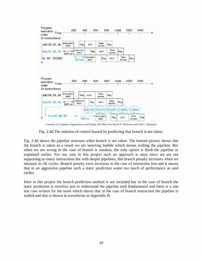
Fig. 2.4d The solution of control hazard by predicting that branch is not taken.
Fig. 2.4d shows the pipeline structure when branch is not taken. The bottom picture shows that
the branch is taken as a result we are inserting bubble which means stalling the pipeline. But
when we are wrong in the case of branch is untaken, the only option is flush the pipeline as
explained earlier. For our case in this project such an approach is okay since we are not
supporting so many instructions but with deeper pipelines, this branch penalty increases when we
measure in clk cycles. Branch penalty even increases in the case of instruction lost and it means
that in an aggressive pipeline such a static prediction waste too much of performance as said
earlier.
Here in this project the branch prediction method is not included but in the case of branch the
static prediction is involves just to understand the pipeline stall fundamental and there is a one
test case written for the same which shows that in the case of branch instruction the pipeline is
stalled and that is shown in waveforms in Appendix B.

20
Chapter 3: Synthesis using Xilinx ISE 13.2
This entire design was synthesized using Xilinx ISE 13.2 tool set. The intention was just analyze
the utilization of Vertex 4 FPGA resources. The table below shows the utilization of resources:
Logic Utilization Used Available Utilization
Total Number of Slice Registers 1024 12,292 9%
Number of used Flip Flops 696 Number of latches 263 Number of 4 inout LUTs 1956 12,292 17%
Logic Distribution
Number of occupied Slices 1208 6144 Number of Slices containing only related logic 1208 1208 Number of Slices containing unrelated logic 0 1208 0%
The Number 4 input LUTs 1958 12,292 17%
Number used as logic 1956 Number used as a route thru 6 Number of bonded IOBs 146 240 61%
Number of BUFG/BUFGCTRLs 2 32 6%
Number used as BUFGs 2 Number used as BUFGCTRLs 0
Table 3a Resource utilization of Vertex 4 FPGA
Above table shows the synthesis report targeting Vertex 4 FPGA, initially it was done for
Spartan 3E, it was just done to show the utilization not much analysis was done or optimization
was implemented since the design only took long time to implement.

21
Chapter 4 : Conclusion and Future work
4.1 Conclusion:
In this practice, I have successfully accomplished building a MIPS CPU with pipeline
functionalities. Data hazard and control hazards are resolved successfully. This design shows the
implementation of MIPS CPU capable of handling various R-type, J-type and I-type of
instruction and each of these categories has a different format. Designing Forwarding unit and
hazard detection unit to overcome the data dependencies was critical task and it was
implemented successfully. This project shows the wide variety of logics to consider during the
design.
This project provided a vital chance to acquire hands on knowledge on MIPS five stage pipeline
processor. Obstacles and problems are sometimes helpful to get more practical knowledge on a
particular subject matter.
4.2 Future Enhancement:
Incorporating memory architecture by designing different CACHE implementation technique
could be helpful to understand the advance computer architecture. Taking this design and dump
it to IC Compiler to understand the physical design fundamental can be a good way to learn
whole ASIC flow.
References

22
1. Computer Organization and Design, 4th
edition by David A. Patterson and John L.
Hennessy
2. IIT Kharagpur video lectures.
3. MIPS Architecture class notes:
http://pages.cs.wisc.edu/~smoler/x86text/lect.notes/MIPS.html (10/24/2012)
4. Synopsys VCS User guide
5. MIPS Architecture and Assembly Language Overview Adapted from:
http://edge.mcs.dre.g.el.edu/GICL/people/sevy/architecture/MIPSRef(SPIM).html
(10/24/2012)
6. UC Berkely and Princeton university’s available online Computer Architecture class
notes
7. Xilinx ISE 13.2 user guide
Appendix A : Different Verilog Code files

23
fetch.v
module fetch(Instruction,Instruction_Reg,PC_+4_reg,flush,clk,Hazard_in,PC_+4,);
input [31:0] Instruction,PC_+4;
input Hazard_in,clk,flush;
output [31:0] Instruction_Reg, PC_+4_reg;
reg [31:0] Instruction_Reg, PC_+4_reg;
initial begin
Instruction_Reg = 0;
PC_+4_reg = 0;
end
always@(posedge clk)
begin
if(flush)
begin
Instruction_Reg <= 0;
PC_+4_reg <=0;
end
else if(~ Hazard_in)
begin
Instruction_Reg <= 32’b0;
PC_+4_reg <= 32’b0;
end
else
Instruction_Reg <= Instruction;
PC_+4_reg <= PC_+4;
end

24
end
end
endmodule
decode.v
module
decode(A_Data,B_Data,immediate_value,RegRs,RegRt,clk,Write_Back,Memory,Execution,A_
Data,RegRd,reg_WriteBack,reg_Memory,Executionreg,
flop_Rs,flop_Rt,flop_Rd,flop_A_Data,flop_B_Data,immediate_valuereg);
input clk;
input [1:0] Write_Back;
output [1:0] reg_WriteBack;
input [2:0] Memory;
output [2:0] reg_Memory;
input [3:0] Execution;
output [3:0]reg_Execution;
input [4:0] RegRs,RegRt,RegRd;
output [4:0] flop_Rs,flop_Rt,flop_Rd
input [31:0] A_Data,B_Data,immediate_value;
output [31:0] flop_A_Data,flop_B_Data,immediate_valuereg;
reg [1:0] reg_WriteBack;
reg [2:0] reg_Memory;
reg [3:0] reg_Execution;
reg [31:0] flop_A_Data,flop_B_Data,immediate_valuereg;
reg [4:0] flop_Rs,flop_Rt,flop_Rd;
initial begin
25
reg_WriteBack = 0;
reg_Memory = 0;
reg_Execution = 0;
flop_A_Data = 0;
flop_B_Data = 0;
immediate_valuereg = 0;
flop_Rs = 0;
flop_Rt = 0;
flop_Rd = 0;
end
always@(posedge clk)
begin
reg_WriteBack <= Write_Back;
reg_Memory <=Memory;
reg_Execution <= Execution;
flop_A_Data <= A_Data;
flop_B_Data <= B_Data;
immediate_valuereg <= immediate_value;
flop_Rs <= RegRs;
flop_Rt <= RegRt;
flop_Rd <= RegRd;
end
endMemoryodule

26
execution.v
module
execution(RegRD,WriteDataIn,flop_Memory,clk,WriteBack,Memory,ALU_out,flop_WriteBack
,flop_ALU,flop_Rd,WriteDataOut);
input clk;
input [1:0] WriteBack;
output [1:0] flop_WriteBack;
input [2:0] Memory;
output [2:0] flop_Memory;
input [4:0] RegRD;
output [4:0] flop_Rd;
input [31:0] ALU_out,WriteDataIn;
output [31:0] flop_ALU,WriteDataOut;
reg [31:0] flop_ALU,WriteDataOut;
reg [4:0] flop_Rd;
reg [1:0] flop_WriteBack;
reg [2:0] flop_Memory;
initial begin
flop_ALU=0;
WriteDataOut=0;
flop_Rd=0;
flop_WriteBack=0;
flop_Memory=0;
end
always@(posedge clk)
begin
flop_WriteBack <= WriteBack;
flop_Memory <= Memory;
flop_ALU <= ALU_out;
flop_Rd <= RegRD;
WriteDataOut <= WriteDataIn;
end
endMemoryodule

27
memory.v
module
Memory_ory(Reg_RD,write_backreg,Memory_reg,ALU_reg,Reg_Rdreg,clk,write_back,Memor
y_out,ALU_Out);
input clk;
input [1:0] write_back;
input [4:0] Reg_RD;
input [31:0] Memory_out,ALU_Out;
output [1:0] write_backreg;
output [31:0] Memory_reg,ALU_reg;
output [4:0] Reg_Rdreg;
reg [1:0] write_backreg;
reg [31:0] Memory_reg,ALU_reg;
reg [4:0] Reg_Rdreg;
initial begin
write_backreg = 0;
Memory_reg = 0;
ALU_reg = 0;
Reg_Rdreg = 0;
end
always@(posedge clk)

28
begin
write_backreg <= write_back;
Memory_reg <= Memory_out;
ALU_reg <= ALU_Out;
Reg_Rdreg <= Reg_RD;
end
endmodule
memory_data.v
module DATAMem(Write_data,Read_data,Mem_Write,Mem_Read,Address,);
input [31:0] Address,Write_data;
input Mem_Write,Mem_Read;
output [31:0] Read_data;
reg [31:0] Read_data;
reg [31:0] regfile[511:0];//32 32-bit registers
always@(Address,Write_data,Mem_Write,Mem_Read)
if(Mem_Write)
begin
regfile[Address]<=Write_data; //Write Operation
end
always@(Address,Write_data,Mem_Write,Mem_Read)

29
if(Mem_Read)
Read_data <= regfile[Address];//read operation
endmodule
memory_instruction.v
module memory_instruction(PC,instruction);
input [31:0] PC;
output [31:0] instruction;
reg [31:0] regfile[511:0];//32 32-bit register
assign instruction = regfile[PC]; //instruction is receiving PC value
endmodule
noclk_mux.v
module nonclk_mux(A,A0,A1,A2,A3,Out);
input [1:0] A;
input [31:0] A3,A2,A1,A0;
output [31:0] Out;
reg [31:0] Out;
always@(A,A3,A2,A1,A0)
begin
case(A)
2’b00:
Out <= A0;
2’b01:
Out <= A1;
2’b10:
Out <= A2;
30
2’b11:
Out <= A3;
endcase
end
endmodule
ALU.v
module ALU_Unit(control_ALU_Unit,DataA,DataB,Result);
input [3:0] control_ALU_Unit; //2^4 =16 possibilities
input [31:0] DataA,DataB; //32 bit data
output [31:0] Result;
reg [31:0] Result;
reg Zero;
initial begin
Result = 32’d0;
end
always@(control_ALU_Unit,DataA,DataB)
begin
case(control_ALU_Unit)
4’b0000: //and instruction
Result <= DataA&DataB;

31
4’b0001: //or instruction
Result <= DataA|DataB;
4’b0010: //add instruction
Result <= DataA+DataB;
4’b0011://multiply instruction
Result <= DataA*DataB;
4’b0100: //nor instruction
begin
Result[0] <= !(DataA[0]|DataB[0]);
Result[1] <= !(DataA[1]|DataB[1]);
Result[2] <= !(DataA[2]|DataB[2]);
Result[3] <= !(DataA[3]|DataB[3]);
Result[4] <= !(DataA[4]|DataB[4]);
Result[5] <= !(DataA[5]|DataB[5]);
Result[6] <= !(DataA[6]|DataB[6]);
Result[7] <= !(DataA[7]|DataB[7]);
Result[8] <= !(DataA[8]|DataB[8]);
Result[9] <= !(DataA[9]|DataB[9]);
Result[10] <= !(DataA[10]|DataB[10]);
Result[11] <= !(DataA[11]|DataB[11]);
Result[12] <= !(DataA[12]|DataB[12]);
Result[13] <= !(DataA[13]|DataB[13]);
32
Result[14] <= !(DataA[14]|DataB[14]);
Result[15] <= !(DataA[15]|DataB[15]);
Result[16] <= !(DataA[16]|DataB[16]);
Result[17] <= !(DataA[17]|DataB[17]);
Result[18] <= !(DataA[18]|DataB[18]);
Result[19] <= !(DataA[19]|DataB[19]);
Result[20] <= !(DataA[20]|DataB[20]);
Result[21] <= !(DataA[21]|DataB[21]);
Result[22] <= !(DataA[22]|DataB[22]);
Result[23] <= !(DataA[23]|DataB[23]);
Result[24] <= !(DataA[24]|DataB[24]);
Result[25] <= !(DataA[25]|DataB[25]);
Result[26] <= !(DataA[26]|DataB[26]);
Result[27] <= !(DataA[27]|DataB[27]);
Result[28] <= !(DataA[28]|DataB[28]);
Result[29] <= !(DataA[29]|DataB[29]);
Result[30] <= !(DataA[30]|DataB[30]);
Result[31] <= !(DataA[31]|DataB[31]);
end
4’b0101: //divide instruction
Result <= DataA/DataB;
4’b0110: //sub instruction
Result <= DataA-DataB;
33
4’b0111: //slt instruction
Result = DataA<DataB ? 1:0;
4’b1000: //sll instruction
Result <= (DataA<<DataB);
4’b0110: //srl instruction
Result <= (DataA>>DataB);
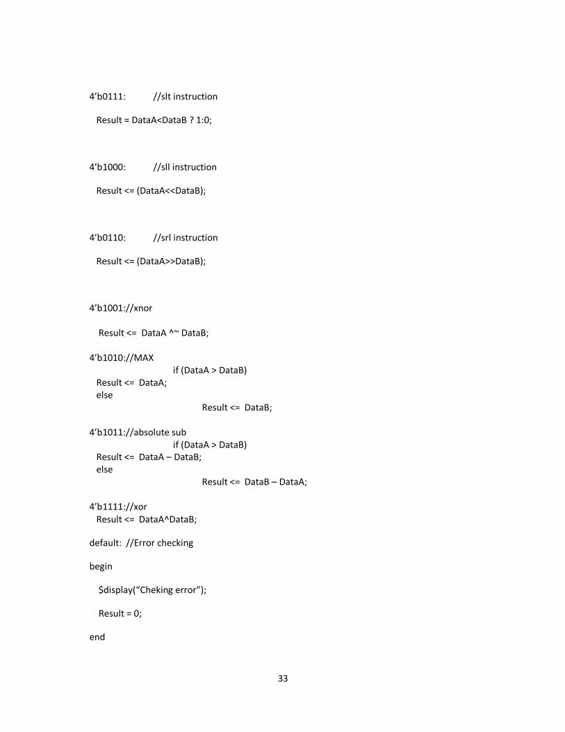
4’b1001://xnor Result <= DataA ^~ DataB; 4’b1010://MAX if (DataA > DataB) Result <= DataA; else Result <= DataB; 4’b1011://absolute sub if (DataA > DataB) Result <= DataA – DataB; else Result <= DataB – DataA; 4’b1111://xor Result <= DataA^DataB;
default: //Error checking
begin
$display(“Cheking error”);
Result = 0;
end

34
endcase
end
endmodule
control_ALU.v
module control_ALU(andi,ori,addi,ALU_Op,operation,ALU_control);
input andi,ori,addi;
input [5:0] operation;
input [1:0] ALU_Op;
output [3:0] ALU_control;
reg [3:0] ALU_control;
always@(ALU_Op or operation or andi or ori or addi)
begin
case(ALU_Op)
2’b00:
ALU_control = 4’b0010;
2’b01:
ALU_control = 4’b0110;
35
2’b10:
begin
if(operation==6’b100100)
ALU_control = 4’b0000;//and
if(operation==6’b100101)
ALU_control = 4’b0001;//or
if(operation==6’b100000)
ALU_control = 4’b0010;//add
if(operation==6’b011000)
ALU_control = 4’b0011;//multi
if(operation==6’b100111)
ALU_control = 4’b0100;//nor
if(operation==6’b011010)
ALU_control = 4’b0101;//div
if(operation==6’b100010)
ALU_control = 4’b0110;//sub
if(operation==6’b101010)
ALU_control = 4’b0111;//slt
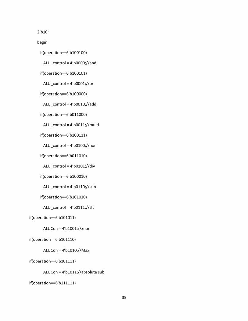
if(operation==6’b101011) ALUCon = 4’b1001;//xnor if(operation==6’b101110) ALUCon = 4’b1010;//Max if(operation==6’b101111) ALUCon = 4’b1011;//absolute sub if(operation==6’b111111)

36
ALUCon = 4’b1111;//xor
end
2’b11:
begin
if(andi)begin
ALU_control = 4’b0000;//andi
end
if(ori) begin
ALU_control = 4’b0001;//ori
end
if(addi)
ALU_control = 4’b0010;//addi
end
endcase
end
endmodule
control_unit.v
//follow chapter 5 from the book
Memoryodule control_unit(Opcode,Out,juMemoryp,bne,immediate,andi,ori,addi);
input [5:0] Opcode;
output[8:0] Out;
output juMemoryp,bne,immediate,andi,ori,addi;

37
wire regdst,alusrc,Memorye_toreg,regwrite,Memorye_read,Memorye_write,branch;
//deterMemoryines type of instruction
wire r = ~Opcode[5]&~Opcode[4]&~Opcode[3]&~Opcode[2]&~Opcode[1]&~Opcode[0];
wire lw = Opcode[5]&~Opcode[4]&~Opcode[3]&~Opcode[2]&Opcode[1]&Opcode[0];
wire sw = Opcode[5]&~Opcode[4]&Opcode[3]&~Opcode[2]&Opcode[1]&Opcode[0];
wire beq = ~Opcode[5]&~Opcode[4]&~Opcode[3]&Opcode[2]&~Opcode[1]&~Opcode[0];
wire bne = ~Opcode[5]&~Opcode[4]&~Opcode[3]&Opcode[2]&~Opcode[1]&Opcode[0];
wire juMemoryp = ~Opcode[5]&~Opcode[4]&~Opcode[3]&~Opcode[2]&Opcode[1]&~Opcode[0];
wire andi = ~Opcode[5]&~Opcode[4]&Opcode[3]&Opcode[2]&~Opcode[1]&~Opcode[0];
wire ori = ~Opcode[5]&~Opcode[4]&Opcode[3]&Opcode[2]&~Opcode[1]&Opcode[0];
wire addi = ~Opcode[5]&~Opcode[4]&Opcode[3]&~Opcode[2]&~Opcode[1]&~Opcode[0];
wire immediate = andi|ori|addi; //
//37on’t37le control arrays for reference
wire [3:0] Execution;
wire [2:0] Memory;
wire [1:0] WriteBack;
// Memoryicrocode control
assign regdst = r;
assign alusrc = lw|sw|immediate;
assign Memorye_toreg = lw;
assign regwrite = r|lw|immediate;

38
assign Memorye_read = lw;
assign Memorye_write = sw;
assign branch = beq;
// Execution control
assign Execution[3] = regdst;
assign Execution[2] = alusrc;
assign Execution[1] = r;
assign Execution[0] = beq;
//Memory control
assign Memory[2] = branch;
assign Memory[1] = Memorye_read;
assign Memory[0] = Memorye_write;
//WriteBack control
assign WriteBack[1] = Memorye_toreg; //not saMemorye as diagraMemory
assign WriteBack[0] = regwrite;
//output control
assign Out[8:7] = WriteBack;
assign Out[6:4] = Memory;
assign Out[3:0] = Execution;
endMemoryodule
39
hazard_detection.v
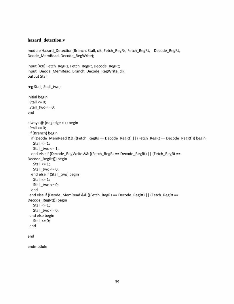
module Hazard_Detection(Branch, Stall, clk ,Fetch_RegRs, Fetch_RegRt, Decode_RegRt, Deode_MemRead, Decode_RegWrite); input [4:0] Fetch_RegRs, Fetch_RegRt, Decode_RegRt; input Deode_MemRead, Branch, Decode_RegWrite, clk; output Stall; reg Stall, Stall_two; initial begin Stall <= 0; Stall_two <= 0; end always @ (negedge clk) begin Stall <= 0; if (Branch) begin if (Deode_MemRead && ((Fetch_RegRs == Decode_RegRt) || (Fetch_RegRt == Decode_RegRt))) begin Stall <= 1; Stall_two <= 1; end else if (Decode_RegWrite && ((Fetch_RegRs == Decode_RegRt) || (Fetch_RegRt == Decode_RegRt))) begin Stall <= 1; Stall_two <= 0; end else if (Stall_two) begin Stall <= 1; Stall_two <= 0; end end else if (Deode_MemRead && ((Fetch_RegRs == Decode_RegRt) || (Fetch_RegRt == Decode_RegRt))) begin Stall <= 1; Stall_two <= 0; end else begin Stall <= 0; end end endmodule

40
forward_data.v
module forward_data(ForwardA, ForwardB, ForwardA_Branch, ForwardB_Branch , Fetch_RegRs, Fetch_RegRt, Branch, Decode_RegRs, Decode_RegRt, Execution_RegWrite, Execution_RegRd, Memory_RegWrite, Memory_RegRd ); input [4:0] Decode_RegRs, Decode_RegRt, Execution_RegRd, Memory_RegRd, Fetch_RegRs, Fetch_RegRt; input Execution_RegWrite, Memory_RegWrite, Branch; output [1:0] ForwardA, ForwardB, ForwardA_Branch, ForwardB_Branch; reg [1:0] ForwardA, ForwardB, ForwardA_Branch, ForwardB_Branch; initial begin ForwardA = 2’b00; ForwardB = 2’b00; ForwardA_Branch = 2’b00; ForwardB_Branch = 2’b00; end always @ (Decode_RegRs or Decode_RegRt or Execution_RegRd or Memory_RegRd or Fetch_RegRs or Fetch_RegRt or Execution_RegWrite or Memory_RegWrite) begin if (Execution_RegWrite && (Execution_RegRd != 5’b0) && (Execution_RegRd == Decode_RegRs)) ForwardA <= 2’b10; else if (Memory_RegWrite && (Memory_RegRd != 5’b0) && (Memory_RegRd == Decode_RegRs)) ForwardA <= 2’b01; else ForwardA <= 2’b00; if (Execution_RegWrite && (Execution_RegRd != 5’b0) && (Execution_RegRd == Decode_RegRt)) ForwardB <= 2’b10; else if (Memory_RegWrite && (Memory_RegRd != 5’b0) && (Memory_RegRd == Decode_RegRt)) ForwardB <= 2’b01; else ForwardB <= 2’b00; if (Branch) begin if (Execution_RegWrite && (Execution_RegRd != 5’b0) && (Execution_RegRd == Fetch_RegRs)) ForwardA_Branch <= 2’b10; else if (Memory_RegWrite && (Memory_RegRd != 5’b0) && (Memory_RegRd == Fetch_RegRs)) ForwardA_Branch <= 2’b01; else

41
ForwardA_Branch <= 2’b00; if (Execution_RegWrite && (Execution_RegRd != 5’b0) && (Execution_RegRd == Fetch_RegRt)) ForwardB_Branch <= 2’b10; else if (Memory_RegWrite && (Memory_RegRd != 5’b0) && (Memory_RegRd == Fetch_RegRt)) ForwardB_Branch <= 2’b01; else ForwardB_Branch <= 2’b00; end end endmodule
cpu_top.v
/**
1. defining 5 stage and control unit variables
2. assign statement //follow chapter 6 carefully
3. port mapping of 5 stages as well control unit, non clk multiplexer and ALU unit.
4. defining cycle 41on’t41le for debugging purpose (VCS)
**/
module cpu_top(clk);
input clk;
//1st stage :fetch_
wire [31:0] nExecution_tpc,fetch_pc_plus_4,fetch_instruction;
reg [31:0] pc;
//2nd stage :decode_
wire PCSrc;
wire [4:0] decode_RegRs,decode_RegRt,decode_RegRd;
wire [31:0] decode_pc_plus_4,decode_instruction;

42
wire [31:0] decode_immediate_value,Branch_Address,PCMuxOut,JumpTarget;
wire [31:0] decode_RegAout, decode_RegBout;
//3rd stage :Execution_
wire [1:0] Execution_WriteBack,Forward_A,Forward_B,alu_op;
wire [4:0] Execution_RegRs,Execution_RegRt,Execution_RegRd,regtopass;
wire [31:0] Execution_RegAout,Execution_RegBout,Execution_immediate_value, b_value;
wire [31:0] Execution_ALUOut,ALU_SrcA,ALU_SrcB;
wire [2:0] Execution_M;
wire [3:0] Execution_Execute,control_ALU;
//4th stage: Memory_
wire [1:0] Memory_WriteBack;
wire [4:0] Mem_RegRd;
wire [31:0] Mem_ALUOut,Memory_WriteData,Mem_ReadData;
wire [2:0] Memory_Mem_;
//5th stage :WriteBack_
wire [1:0] WriteBack_WriteBack_;
wire [4:0] WriteBack_RegRd;
wire [31:0] datatowrite,WriteBack_ReadData,WriteBack_ALUOut;
// control at decode_ stage
wire PC_Write,fetch_decode_Write,Hazard_mux_control,jump,bne,immediate,andi,ori,addi;
wire [8:0] decode_control,out_control;
//cycle count for debugging (VCS)
reg [31:0] cycle;
//initial conditions
43
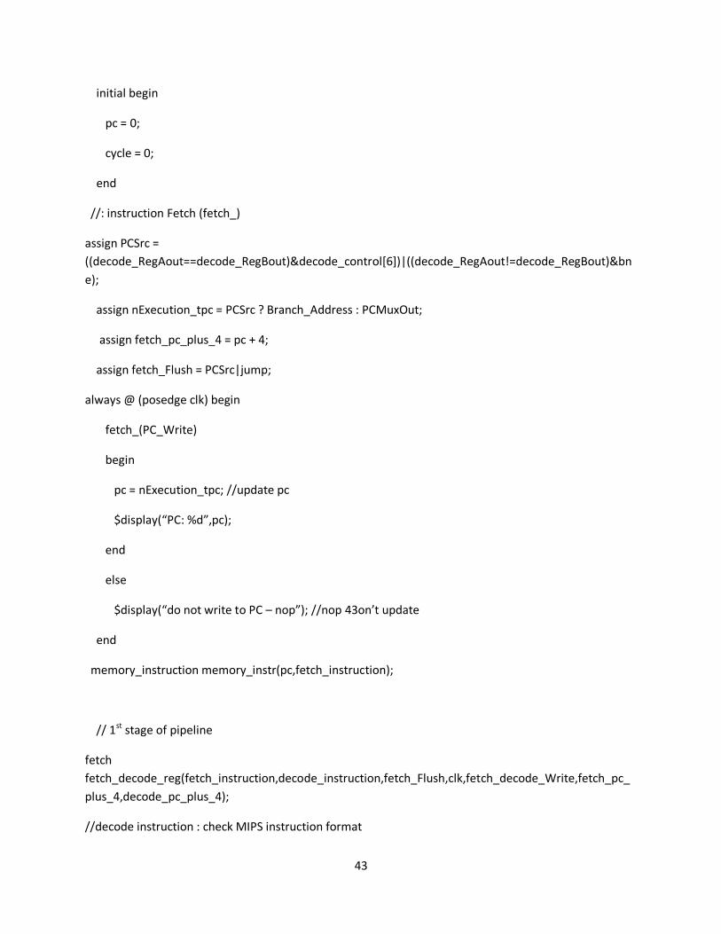
initial begin
pc = 0;
cycle = 0;
end
//: instruction Fetch (fetch_)
assign PCSrc =
((decode_RegAout==decode_RegBout)&decode_control[6])|((decode_RegAout!=decode_RegBout)&bn
e);
assign nExecution_tpc = PCSrc ? Branch_Address : PCMuxOut;
assign fetch_pc_plus_4 = pc + 4;
assign fetch_Flush = PCSrc|jump;
always @ (posedge clk) begin
fetch_(PC_Write)
begin
pc = nExecution_tpc; //update pc
$display(“PC: %d”,pc);
end
else
$display(“do not write to PC – nop”); //nop 43on’t update
end
memory_instruction memory_instr(pc,fetch_instruction);
// 1st stage of pipeline
fetch
fetch_decode_reg(fetch_instruction,decode_instruction,fetch_Flush,clk,fetch_decode_Write,fetch_pc_
plus_4,decode_pc_plus_4);
//decode instruction : check MIPS instruction format
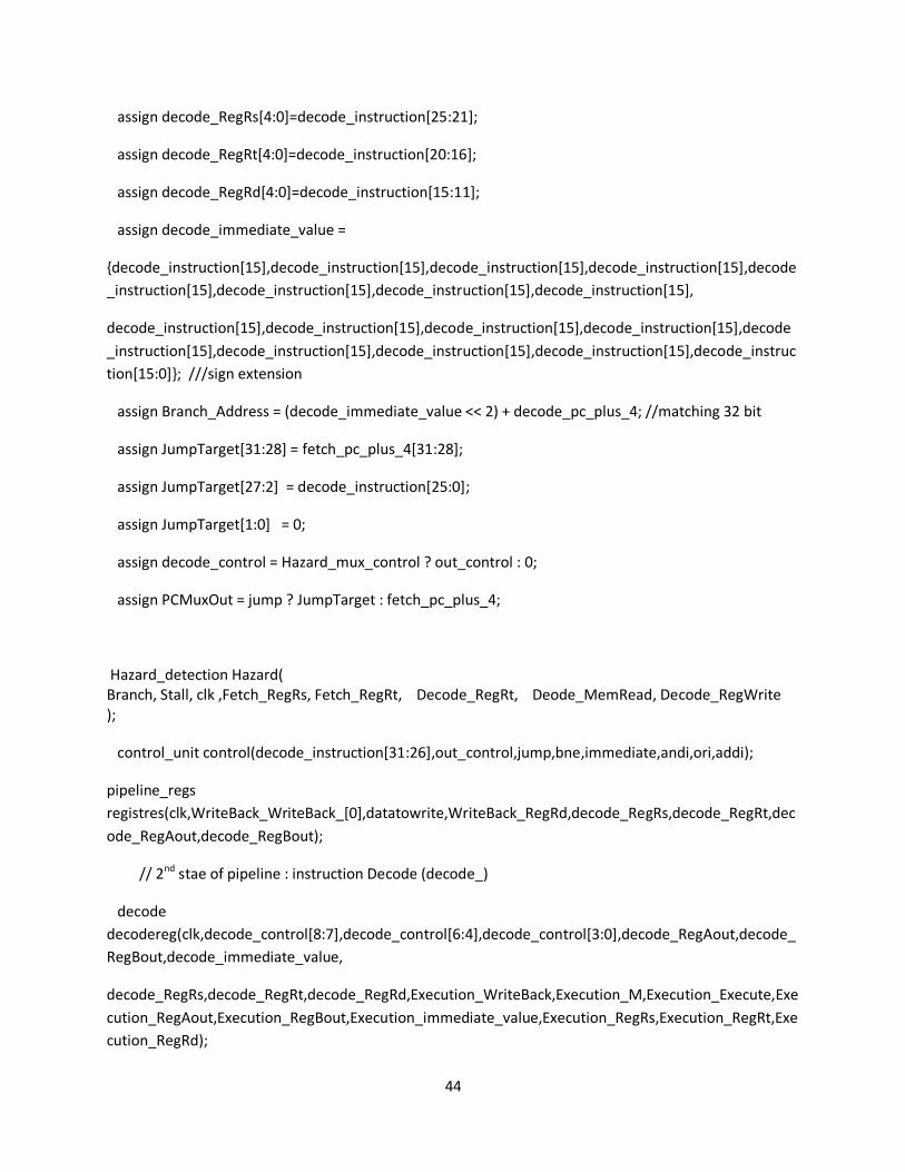
44
assign decode_RegRs[4:0]=decode_instruction[25:21];
assign decode_RegRt[4:0]=decode_instruction[20:16];
assign decode_RegRd[4:0]=decode_instruction[15:11];
assign decode_immediate_value =
{decode_instruction[15],decode_instruction[15],decode_instruction[15],decode_instruction[15],decode
_instruction[15],decode_instruction[15],decode_instruction[15],decode_instruction[15],
decode_instruction[15],decode_instruction[15],decode_instruction[15],decode_instruction[15],decode
_instruction[15],decode_instruction[15],decode_instruction[15],decode_instruction[15],decode_instruc
tion[15:0]}; ///sign extension
assign Branch_Address = (decode_immediate_value << 2) + decode_pc_plus_4; //matching 32 bit
assign JumpTarget[31:28] = fetch_pc_plus_4[31:28];
assign JumpTarget[27:2] = decode_instruction[25:0];
assign JumpTarget[1:0] = 0;
assign decode_control = Hazard_mux_control ? out_control : 0;
assign PCMuxOut = jump ? JumpTarget : fetch_pc_plus_4;
Hazard_detection Hazard( Branch, Stall, clk ,Fetch_RegRs, Fetch_RegRt, Decode_RegRt, Deode_MemRead, Decode_RegWrite );
control_unit control(decode_instruction[31:26],out_control,jump,bne,immediate,andi,ori,addi);
pipeline_regs
registres(clk,WriteBack_WriteBack_[0],datatowrite,WriteBack_RegRd,decode_RegRs,decode_RegRt,dec
ode_RegAout,decode_RegBout);
// 2nd stae of pipeline : instruction Decode (decode_)
decode
decodereg(clk,decode_control[8:7],decode_control[6:4],decode_control[3:0],decode_RegAout,decode_
RegBout,decode_immediate_value,
decode_RegRs,decode_RegRt,decode_RegRd,Execution_WriteBack,Execution_M,Execution_Execute,Exe
cution_RegAout,Execution_RegBout,Execution_immediate_value,Execution_RegRs,Execution_RegRt,Exe
cution_RegRd);
45
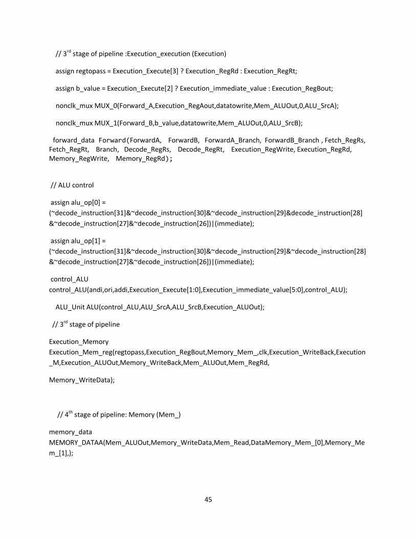
// 3rd stage of pipeline :Execution_execution (Execution)
assign regtopass = Execution_Execute[3] ? Execution_RegRd : Execution_RegRt;
assign b_value = Execution_Execute[2] ? Execution_immediate_value : Execution_RegBout;
nonclk_mux MUX_0(Forward_A,Execution_RegAout,datatowrite,Mem_ALUOut,0,ALU_SrcA);
nonclk_mux MUX_1(Forward_B,b_value,datatowrite,Mem_ALUOut,0,ALU_SrcB);
forward_data Forward(ForwardA, ForwardB, ForwardA_Branch, ForwardB_Branch , Fetch_RegRs, Fetch_RegRt, Branch, Decode_RegRs, Decode_RegRt, Execution_RegWrite, Execution_RegRd, Memory_RegWrite, Memory_RegRd);
// ALU control
assign alu_op[0] =
(~decode_instruction[31]&~decode_instruction[30]&~decode_instruction[29]&decode_instruction[28]
&~decode_instruction[27]&~decode_instruction[26])|(immediate);
assign alu_op[1] =
(~decode_instruction[31]&~decode_instruction[30]&~decode_instruction[29]&~decode_instruction[28]
&~decode_instruction[27]&~decode_instruction[26])|(immediate);
control_ALU
control_ALU(andi,ori,addi,Execution_Execute[1:0],Execution_immediate_value[5:0],control_ALU);
ALU_Unit ALU(control_ALU,ALU_SrcA,ALU_SrcB,Execution_ALUOut);
// 3rd stage of pipeline
Execution_Memory
Execution_Mem_reg(regtopass,Execution_RegBout,Memory_Mem_,clk,Execution_WriteBack,Execution
_M,Execution_ALUOut,Memory_WriteBack,Mem_ALUOut,Mem_RegRd,
Memory_WriteData);
// 4th stage of pipeline: Memory (Mem_)
memory_data
MEMORY_DATAA(Mem_ALUOut,Memory_WriteData,Mem_Read,DataMemory_Mem_[0],Memory_Me
m_[1],);

46
Memory
Memory_WriteBackreg(Mem_RegRd,WriteBack_WriteBack_,WriteBack_ReadData,WriteBack_ALUOut,
WriteBack_RegRd,clk,Memory_WriteBack,Mem_ReadData,Mem_ALUOut);
// 5th stage of pipeline :Write Back (WriteBack)
assign datatowrite = WriteBack_WriteBack_[1] ? WriteBack_ReadData : WriteBack_ALUOut;
//debugging variable , check in waveform
always@(posedge clk)
begin
cycle = cycle + 1;
end
endmodule
tb_cpu.v
module tb_cpu;
integer i;
reg Clk;
initial
begin
$vcdplusfile(“cpu.vpd”);
$vcdpluson;
$vcdplusmemon;
end

47
initial begin
Clk = 1;
end
//clk controls
always begin
clk = ~clk;
#25;
end
initial begin
// Initilization of Instruction Memory
Instruction_Memory_register[0] = 32’h012A4020; //add R5,R3,R4
Instruction_Memory_register[4] = 32’h012A4023; //sub R6,R5,R4
Instruction_Memory_register[8] = 32’h2128000C; //addi R3, R3, 12
Instruction_Memory_register[12] = 32’h01090018; //mult $t0, $t1
Instruction_Memory_register[16] = 32’h0109001B;//j
Instruction_Memory_register[20] = 32’h012A4024; // and R7,R3,R4
Instruction_Memory_register[24] = 32’h00094280; //sll R5,R11,R3
Instruction_Memory_register[28] = 32’h0094282A;//srl R6,R7,R9
Instruction_Memory_register[32] = 32’h8D28000C; //lw R4,1(R0)
Instruction_Memory_register[36] = 32’hAD28000C; //add R5,R3,R4
Instruction_Memory_register[40] = 32’h1509000C; //bne $t0, $t1, 12
Instruction_Memory_register[44] = 32’h012A402A; //slt R10,R6,R5
Instruction_Memory_register[48] = 32’h0166601A;//div R12,R11,R6
Instruction_Memory_register[52] = 32’h34CE0002;//ori R14,R6,2
48
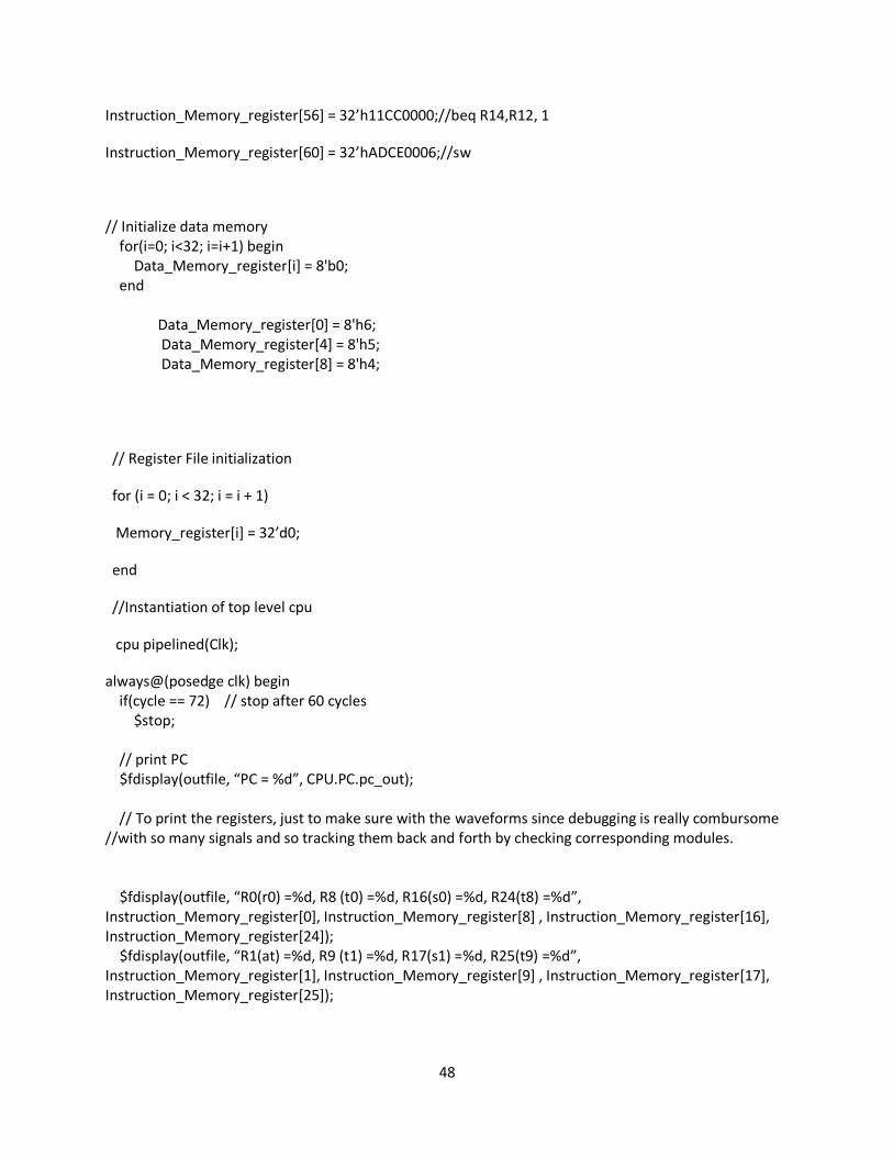
Instruction_Memory_register[56] = 32’h11CC0000;//beq R14,R12, 1
Instruction_Memory_register[60] = 32’hADCE0006;//sw
// Initialize data memory for(i=0; i<32; i=i+1) begin Data_Memory_register[i] = 8'b0; end Data_Memory_register[0] = 8'h6; Data_Memory_register[4] = 8'h5; Data_Memory_register[8] = 8'h4;
// Register File initialization
for (i = 0; i < 32; i = i + 1)
Memory_register[i] = 32’d0;
end
//Instantiation of top level cpu
cpu pipelined(Clk);
always@(posedge clk) begin if(cycle == 72) // stop after 60 cycles $stop; // print PC $fdisplay(outfile, “PC = %d”, CPU.PC.pc_out); // To print the registers, just to make sure with the waveforms since debugging is really combursome //with so many signals and so tracking them back and forth by checking corresponding modules. $fdisplay(outfile, “R0(r0) =%d, R8 (t0) =%d, R16(s0) =%d, R24(t8) =%d”, Instruction_Memory_register[0], Instruction_Memory_register[8] , Instruction_Memory_register[16], Instruction_Memory_register[24]); $fdisplay(outfile, “R1(at) =%d, R9 (t1) =%d, R17(s1) =%d, R25(t9) =%d”, Instruction_Memory_register[1], Instruction_Memory_register[9] , Instruction_Memory_register[17], Instruction_Memory_register[25]);

49
$fdisplay(outfile, “R2(v0) =%d, R10(t2) =%d, R18(s2) =%d, R26(k0) =%d”, Instruction_Memory_register[2], Instruction_Memory_register[10], Instruction_Memory_register[18], Instruction_Memory_register[26]); $fdisplay(outfile, “R3(v1) =%d, R11(t3) =%d, R19(s3) =%d, R27(k1) =%d”, Instruction_Memory_register[3], Instruction_Memory_register[11], Instruction_Memory_register[19], Instruction_Memory_register[27]); $fdisplay(outfile, “R4(a0) =%d, R12(t4) =%d, R20(s4) =%d, R28(gp) =%d”, Instruction_Memory_register[4], Instruction_Memory_register[12], Instruction_Memory_register[20], Instruction_Memory_register[28]); $fdisplay(outfile, “R5(a1) =%d, R13(t5) =%d, R21(s5) =%d, R29(sp) =%d”, Instruction_Memory_register[5], Instruction_Memory_register[13], Instruction_Memory_register[21], Instruction_Memory_register[29]); $fdisplay(outfile, “R6(a2) =%d, R14(t6) =%d, R22(s6) =%d, R30(s8) =%d”, Instruction_Memory_register[6], Instruction_Memory_register[14], Instruction_Memory_register[22], Instruction_Memory_register[30]); $fdisplay(outfile, “R7(a3) =%d, R15(t7) =%d, R23(s7) =%d, R31(ra) =%d”, Instruction_Memory_register[7], Instruction_Memory_register[15], Instruction_Memory_register[23], Instruction_Memory_register[31]); cycle = cycle + 1; end endmodule

50
Appendix B : Output
B.1 initial information form vcs.log Chronologic VCS ©
Version G-2012.09 – Wed Oct 11 16:50:47 2012
Copyright © 1991-2012 by Synopsys Inc.
ALL RIGHTS RESERVED
This program is proprietary and confidential information of Synopsys Inc.
and may be used and disclosed only as authorized in a license agreement
controlling such use and disclosure.
Warning-[DFLT_OPT] Default option found
Option ‘-ntb_opts dtm’ is already default. Future releases of VCS may
not
accept ‘-ntb_opts dtm’.
Warning-[OBSLFLGS] Obsolete flag(s) used
The flag(s) ‘-no_error’ is(are) obsolete and will not be supported
courtesy of
this release. Please use ‘-error=no<ID>’ instead.
Please contact [email protected] or call VCS Customer Support at
1-800-VERILOG for any questions about obsolete switches.
Warning-[LCA_FEATURES_ENABLED] Usage warning
LCA features enabled by ‘-lca’ argument on the command line. For more
information regarding list of LCA features please refer to Chapter “LCA
features” in the VCS/VCS-MX Release Notes
Parsing design file ‘../../arc_6300/TESTBENCH/MIPS/tb_cpu.v’
Parsing design file ‘../RTL/MIPS/Control_unit.v’
Parsing design file ‘../RTL/MIPS/control_ALU.v’
Parsing design file ‘../RTL/MIPS/ALU_unit.v’
Parsing design file ‘../RTL/MIPS/noclk_mux.v’
Parsing design file ‘../RTL/MIPS/memory_data.v’
Parsing design file ‘../RTL/MIPS/execution.v’
Parsing design file ‘../RTL/MIPS/Hazard_detection.v’
Parsing design file ‘../RTL/MIPS/decode.v’
Parsing design file ‘../RTL/MIPS/fetch.v’
Parsing design file ‘../RTL/MIPS/memory_instruction.v’
Parsing design file ‘../RTL/MIPS/memory.v’
Parsing design file ‘../RTL/MIPS/pipeline_regs.v’
Parsing design file ‘../RTL/MIPS/Forward_data.v’
Parsing design file ‘../RTL/MIPS/cpu_top.v’
Top Level Modules:
tb_cpu
No TimeScale specified
Starting vcs inline pass...
modules and 0 UDP read.

51
However, due to incremental compilation, no re-compilation is
necessary.
Ld –r –m elf_i386 –o pre_vcsobj_1_1.o –whole-archive pre_vcsobj_1_1.a –no-
whole-archive
if [ -x ../simv ]; then chmod –x ../simv; fi
g++ -o ../simv –melf_i386 –m32 -Wl,-whole-archive -Wl,-no-whole-
archive SIM_l.o 5NrI_d.o 5NrIB_d.o pre_vcsobj_1_1.o rmapats_mop.o
rmapats.o /global/apps3/vcs_2012.09/linux/lib/libnplex_stub.so
/global/apps3/vcs_2012.09/linux/lib/libvirsim.so
/global/apps3/vcs_2012.09/linux/lib/librterrorinf.so
/global/apps3/vcs_2012.09/linux/lib/libsnpsmalloc.so
/global/apps3/vcs_2012.09/linux/lib/libvcsnew.so
/global/apps3/vcs_2012.09/linux/lib/libreader_common.so
/global/apps3/vcs_2012.09/linux/lib/libBA.a
/global/apps3/vcs_2012.09/linux/lib/libuclinative.so
/global/apps3/vcs_2012.09/linux/lib/vcs_save_restore_new.o
/global/apps3/vcs_2012.09/linux/lib/ctype-stubs_32.a –ldl –lm -lc –
lpthread –ldl
../simv up to date
Warning-[LCA_FEATURES_ENABLED] Usage warning
LCA features enabled by ‘-lca’ argument on the command line. For more
information regarding list of LCA features please refer to Chapter “LCA
features” in the VCS/VCS-MX Release Notes
Chronologic VCS simulator copyright 1991-2012
Contains Synopsys proprietary information.
Compiler version G-2012.09; Runtime version G-2012.09; Oct 10 16:50 2012
VCD+ Writer G-2012.09 Copyright © 1991-2012 by Synopsys

52
B.2 Waveforms:
First screenshot shows the cycle count as well all the stages and correspondent register value.
Fig. B.2a 1st screenshot of simulation waveform
This waveform in Fig. B.2a shows that the different instructions are loaded correctly and are
being clocked from the fetch unit to decode unit that means our decode unit is working correctly
as well instruction memory and of course fetch unit. If we examine this waveform carefully then
we can see that at every clock edge the instruction is being transferred to decode stage from fetch
stage. So as written in testbench for correspondent PC , we can see that instruction is loaded in
the unit correctly.
Below in Fig. B.2b, waveform again shows that the instructions are being loaded correctly as per
the written test cases. Here in this and waveform B.2c if check carefully the PC number 40 then
it is trying to execute one of the odd test case which tests CPU in the case of data hazard where
we need to stall the pipeline to execute the subsequent instruction correctly. Below is the specific
test case from testbench where we must need to stall the pipeline and that is the example that
shows our hazard detection unit is working fine. Please do not confuse with the PC number since
in waveform it is always one PC ahead then we have in testbench since we can see working

53
instruction in CPU unit only in decode stage and that one cycle after fetch unit fetches from
Instruction Memory.
Instruction_Memory_register[32] = 32’h8D28000C; //lw R4,1(R0)
Instruction_Memory_register[36] = 32’hAD28000C; //add R5,R3,R4
So, this is the particular test where in add instruction wants to use R4 that is the destination
register (write) for load word instruction. Now load is the longest instruction that travels all five
stages of the pipeline and this is where out hazard detection policy comes in to the action and
saving our CPU from being frozen for more number of cycles.
Fig., B.2b 2nd
screenshot of simulation waveform
In this specific case in Fig. B.2b and B.2c cycle number 10 and 11 is devoted for one instruction
only that means pipeline is stalled for one cycle and subsequent instruction will work from cycle
number 12. Please check the hazard_in signal carefully it is at logic low as in RTL it was
considered that in order to stall the pipeline all the affected signals should be given zero and
hazard_in signal is the indication of that. Again since at PC number 32 which is 36 here in this
waveform , the instruction is load and so reg_Memory.. signal shows that we are accessing the
memory.

54
Fig., B.2c 2
nd screenshot of simulation waveform
Fig. B.2d is another example of stall but this time it is due to branch instruction as well store
word instruction. This is the case where testbench is testing the CPU extensively two back to
back cases where stall should be apply to work ahead and waveform B.2d shows that it happens
correctly. To understand the functionality of the pipeline please examine the signals Branch,
Branch_zero and Branch_taken and the flush is applied to flush the pipeline which we can see by
watching flush signal and so correspondent decoded instruction which is nothing. And then after
from cycle number 19 now again pipeline has started working for the next instruction.

55
Fig., B.2d 2nd
screenshot of simulation waveform

56
Appendix C: Use of VCS simulator
There were different switches were used to simulate this design appropriately as per the
requirement developed UNIX directory tree structure. This chapter explains different used
switches and details of each...This section is reference from Synopsys VCS user guide. [4]
The command used to simulate the design in VCS MX:
vcs -ova_cov -debug_all -ntb_opts dtm -ova_cov -sverilog +v2k -l vcs.log -R -sverilog -no_error
ZONMCM +incdir+../RTL/MIPS+../TESTBENCH/MIPS -f ../TESTBENCH/tb_cpu.vc -f ec4.vc
-lca +vcs+vcdpluson +plusarg_ignore -assert enable_diag
Below is the detail of corresponding options (switches)
-ova_file filename
This command is used to identify which filename is asseeted. If we are asserting multiple files
then this switch should be used multiple times.
-debug_all
To simulate the current design in interactive mode this compile time option needs to be used.
-verilog =V2k -1 vcs.log
To point at the latest Verilog revision and correspondent vcs log.
-no_error ZONMCM
It changes the following errors in to warning message and allows VCS MX to create executable
simv courtesy of displaying warning message: [4]
“Error-[ZMMCM] Zero multiconcat multiplier cannot be used in this context
A replication with a zero replication constant is considered to have
a size of zero and is ignored. Such a replication shall appear
only within a concatenation in which at least one of the
operands of the concatenation have a positive size.
target : {0 {1'bx}}
Error-[NMCM] Negative multiconcat multiplier
target : {(-1) {1'bx}}
"my_test.v", 6” [4]
+incdir+
This includes the current directory structure.
+vcs+vcdpluson
57
To enable the dumping for the entire design this switch needs to be used.
+plusarg_ignore
This command is used to tell the VCS MX not to compile certain runtime options.
-assert enable_diag
This command is used to enable the control of the results that reports to runtime options. Runt
time assert options are enables only if we use this switch.

58
Appendix D: Schematic view of Design